EP2730634B1 - Novel compound and organic electronic device using same - Google Patents
Novel compound and organic electronic device using same Download PDFInfo
- Publication number
- EP2730634B1 EP2730634B1 EP12810891.7A EP12810891A EP2730634B1 EP 2730634 B1 EP2730634 B1 EP 2730634B1 EP 12810891 A EP12810891 A EP 12810891A EP 2730634 B1 EP2730634 B1 EP 2730634B1
- Authority
- EP
- European Patent Office
- Prior art keywords
- formula
- group
- compound
- organic
- light emitting
- Prior art date
- Legal status (The legal status is an assumption and is not a legal conclusion. Google has not performed a legal analysis and makes no representation as to the accuracy of the status listed.)
- Active
Links
- BHWYCEUWXZFNKZ-UHFFFAOYSA-N CC1(C)OB(c(cc2)cc(c3c4c(cccc5)c5cc3)c2[n]2c4nc3ccccc23)OC1(C)C Chemical compound CC1(C)OB(c(cc2)cc(c3c4c(cccc5)c5cc3)c2[n]2c4nc3ccccc23)OC1(C)C BHWYCEUWXZFNKZ-UHFFFAOYSA-N 0.000 description 1
- DZJMHURWDQGZGP-UHFFFAOYSA-N CC1(C)OB(c2cc(c3ccccc3[n]3c4nc5c3cccc5)c4c3c2cccc3)OC1(C)C Chemical compound CC1(C)OB(c2cc(c3ccccc3[n]3c4nc5c3cccc5)c4c3c2cccc3)OC1(C)C DZJMHURWDQGZGP-UHFFFAOYSA-N 0.000 description 1
- ZOAHGBSHRUDPAE-UHFFFAOYSA-N CC1(C)OB(c2ccc(c3c(c4nc(c(cccc5)c5cc5)c5[n]44)c(cccc5)c5cc3)c4c2)OC1(C)C Chemical compound CC1(C)OB(c2ccc(c3c(c4nc(c(cccc5)c5cc5)c5[n]44)c(cccc5)c5cc3)c4c2)OC1(C)C ZOAHGBSHRUDPAE-UHFFFAOYSA-N 0.000 description 1
- XXWGTROKOFVWOS-UHFFFAOYSA-N Clc1cc(c(cccc2)c2[n]2c3nc4ccccc24)c3c2c1cccc2 Chemical compound Clc1cc(c(cccc2)c2[n]2c3nc4ccccc24)c3c2c1cccc2 XXWGTROKOFVWOS-UHFFFAOYSA-N 0.000 description 1
- ZEBPUNAJMQLOGL-UHFFFAOYSA-N c(cc1)ccc1-c(cc1)ccc1-c(cc1)cc([n]2c3nc4c2ccc2c4cccc2)c1c1c3c(cccc2)c2cc1 Chemical compound c(cc1)ccc1-c(cc1)ccc1-c(cc1)cc([n]2c3nc4c2ccc2c4cccc2)c1c1c3c(cccc2)c2cc1 ZEBPUNAJMQLOGL-UHFFFAOYSA-N 0.000 description 1
- HLOFGSXMSKMNMP-UHFFFAOYSA-N c(cc12)ccc1nc1[n]2c(ccc(-c2cc(-c3ccc(c4ccccc4c4c5cccc4)c5c3)ccc2)c2)c2c2c1c(cccc1)c1cc2 Chemical compound c(cc12)ccc1nc1[n]2c(ccc(-c2cc(-c3ccc(c4ccccc4c4c5cccc4)c5c3)ccc2)c2)c2c2c1c(cccc1)c1cc2 HLOFGSXMSKMNMP-UHFFFAOYSA-N 0.000 description 1
Images


Classifications
-
- C—CHEMISTRY; METALLURGY
- C07—ORGANIC CHEMISTRY
- C07D—HETEROCYCLIC COMPOUNDS
- C07D471/00—Heterocyclic compounds containing nitrogen atoms as the only ring hetero atoms in the condensed system, at least one ring being a six-membered ring with one nitrogen atom, not provided for by groups C07D451/00 - C07D463/00
- C07D471/02—Heterocyclic compounds containing nitrogen atoms as the only ring hetero atoms in the condensed system, at least one ring being a six-membered ring with one nitrogen atom, not provided for by groups C07D451/00 - C07D463/00 in which the condensed system contains two hetero rings
- C07D471/04—Ortho-condensed systems
-
- C—CHEMISTRY; METALLURGY
- C07—ORGANIC CHEMISTRY
- C07D—HETEROCYCLIC COMPOUNDS
- C07D471/00—Heterocyclic compounds containing nitrogen atoms as the only ring hetero atoms in the condensed system, at least one ring being a six-membered ring with one nitrogen atom, not provided for by groups C07D451/00 - C07D463/00
- C07D471/12—Heterocyclic compounds containing nitrogen atoms as the only ring hetero atoms in the condensed system, at least one ring being a six-membered ring with one nitrogen atom, not provided for by groups C07D451/00 - C07D463/00 in which the condensed system contains three hetero rings
- C07D471/14—Ortho-condensed systems
-
- C—CHEMISTRY; METALLURGY
- C07—ORGANIC CHEMISTRY
- C07D—HETEROCYCLIC COMPOUNDS
- C07D487/00—Heterocyclic compounds containing nitrogen atoms as the only ring hetero atoms in the condensed system, not provided for by groups C07D451/00 - C07D477/00
- C07D487/02—Heterocyclic compounds containing nitrogen atoms as the only ring hetero atoms in the condensed system, not provided for by groups C07D451/00 - C07D477/00 in which the condensed system contains two hetero rings
- C07D487/04—Ortho-condensed systems
-
- C—CHEMISTRY; METALLURGY
- C09—DYES; PAINTS; POLISHES; NATURAL RESINS; ADHESIVES; COMPOSITIONS NOT OTHERWISE PROVIDED FOR; APPLICATIONS OF MATERIALS NOT OTHERWISE PROVIDED FOR
- C09K—MATERIALS FOR MISCELLANEOUS APPLICATIONS, NOT PROVIDED FOR ELSEWHERE
- C09K11/00—Luminescent materials, e.g. electroluminescent or chemiluminescent
- C09K11/06—Luminescent materials, e.g. electroluminescent or chemiluminescent containing organic luminescent materials
-
- H—ELECTRICITY
- H10—SEMICONDUCTOR DEVICES; ELECTRIC SOLID-STATE DEVICES NOT OTHERWISE PROVIDED FOR
- H10K—ORGANIC ELECTRIC SOLID-STATE DEVICES
- H10K50/00—Organic light-emitting devices
- H10K50/10—OLEDs or polymer light-emitting diodes [PLED]
- H10K50/11—OLEDs or polymer light-emitting diodes [PLED] characterised by the electroluminescent [EL] layers
- H10K50/12—OLEDs or polymer light-emitting diodes [PLED] characterised by the electroluminescent [EL] layers comprising dopants
-
- H—ELECTRICITY
- H10—SEMICONDUCTOR DEVICES; ELECTRIC SOLID-STATE DEVICES NOT OTHERWISE PROVIDED FOR
- H10K—ORGANIC ELECTRIC SOLID-STATE DEVICES
- H10K85/00—Organic materials used in the body or electrodes of devices covered by this subclass
- H10K85/60—Organic compounds having low molecular weight
- H10K85/615—Polycyclic condensed aromatic hydrocarbons, e.g. anthracene
-
- H—ELECTRICITY
- H10—SEMICONDUCTOR DEVICES; ELECTRIC SOLID-STATE DEVICES NOT OTHERWISE PROVIDED FOR
- H10K—ORGANIC ELECTRIC SOLID-STATE DEVICES
- H10K85/00—Organic materials used in the body or electrodes of devices covered by this subclass
- H10K85/60—Organic compounds having low molecular weight
- H10K85/615—Polycyclic condensed aromatic hydrocarbons, e.g. anthracene
- H10K85/622—Polycyclic condensed aromatic hydrocarbons, e.g. anthracene containing four rings, e.g. pyrene
-
- H—ELECTRICITY
- H10—SEMICONDUCTOR DEVICES; ELECTRIC SOLID-STATE DEVICES NOT OTHERWISE PROVIDED FOR
- H10K—ORGANIC ELECTRIC SOLID-STATE DEVICES
- H10K85/00—Organic materials used in the body or electrodes of devices covered by this subclass
- H10K85/60—Organic compounds having low molecular weight
- H10K85/615—Polycyclic condensed aromatic hydrocarbons, e.g. anthracene
- H10K85/623—Polycyclic condensed aromatic hydrocarbons, e.g. anthracene containing five rings, e.g. pentacene
-
- H—ELECTRICITY
- H10—SEMICONDUCTOR DEVICES; ELECTRIC SOLID-STATE DEVICES NOT OTHERWISE PROVIDED FOR
- H10K—ORGANIC ELECTRIC SOLID-STATE DEVICES
- H10K85/00—Organic materials used in the body or electrodes of devices covered by this subclass
- H10K85/60—Organic compounds having low molecular weight
- H10K85/615—Polycyclic condensed aromatic hydrocarbons, e.g. anthracene
- H10K85/624—Polycyclic condensed aromatic hydrocarbons, e.g. anthracene containing six or more rings
-
- H—ELECTRICITY
- H10—SEMICONDUCTOR DEVICES; ELECTRIC SOLID-STATE DEVICES NOT OTHERWISE PROVIDED FOR
- H10K—ORGANIC ELECTRIC SOLID-STATE DEVICES
- H10K85/00—Organic materials used in the body or electrodes of devices covered by this subclass
- H10K85/60—Organic compounds having low molecular weight
- H10K85/615—Polycyclic condensed aromatic hydrocarbons, e.g. anthracene
- H10K85/626—Polycyclic condensed aromatic hydrocarbons, e.g. anthracene containing more than one polycyclic condensed aromatic rings, e.g. bis-anthracene
-
- H—ELECTRICITY
- H10—SEMICONDUCTOR DEVICES; ELECTRIC SOLID-STATE DEVICES NOT OTHERWISE PROVIDED FOR
- H10K—ORGANIC ELECTRIC SOLID-STATE DEVICES
- H10K85/00—Organic materials used in the body or electrodes of devices covered by this subclass
- H10K85/60—Organic compounds having low molecular weight
- H10K85/631—Amine compounds having at least two aryl rest on at least one amine-nitrogen atom, e.g. triphenylamine
- H10K85/636—Amine compounds having at least two aryl rest on at least one amine-nitrogen atom, e.g. triphenylamine comprising heteroaromatic hydrocarbons as substituents on the nitrogen atom
-
- H—ELECTRICITY
- H10—SEMICONDUCTOR DEVICES; ELECTRIC SOLID-STATE DEVICES NOT OTHERWISE PROVIDED FOR
- H10K—ORGANIC ELECTRIC SOLID-STATE DEVICES
- H10K85/00—Organic materials used in the body or electrodes of devices covered by this subclass
- H10K85/60—Organic compounds having low molecular weight
- H10K85/649—Aromatic compounds comprising a hetero atom
- H10K85/654—Aromatic compounds comprising a hetero atom comprising only nitrogen as heteroatom
-
- H—ELECTRICITY
- H10—SEMICONDUCTOR DEVICES; ELECTRIC SOLID-STATE DEVICES NOT OTHERWISE PROVIDED FOR
- H10K—ORGANIC ELECTRIC SOLID-STATE DEVICES
- H10K85/00—Organic materials used in the body or electrodes of devices covered by this subclass
- H10K85/60—Organic compounds having low molecular weight
- H10K85/649—Aromatic compounds comprising a hetero atom
- H10K85/657—Polycyclic condensed heteroaromatic hydrocarbons
- H10K85/6572—Polycyclic condensed heteroaromatic hydrocarbons comprising only nitrogen in the heteroaromatic polycondensed ring system, e.g. phenanthroline or carbazole
-
- H—ELECTRICITY
- H10—SEMICONDUCTOR DEVICES; ELECTRIC SOLID-STATE DEVICES NOT OTHERWISE PROVIDED FOR
- H10K—ORGANIC ELECTRIC SOLID-STATE DEVICES
- H10K85/00—Organic materials used in the body or electrodes of devices covered by this subclass
- H10K85/60—Organic compounds having low molecular weight
- H10K85/649—Aromatic compounds comprising a hetero atom
- H10K85/657—Polycyclic condensed heteroaromatic hydrocarbons
- H10K85/6574—Polycyclic condensed heteroaromatic hydrocarbons comprising only oxygen in the heteroaromatic polycondensed ring system, e.g. cumarine dyes
-
- H—ELECTRICITY
- H10—SEMICONDUCTOR DEVICES; ELECTRIC SOLID-STATE DEVICES NOT OTHERWISE PROVIDED FOR
- H10K—ORGANIC ELECTRIC SOLID-STATE DEVICES
- H10K85/00—Organic materials used in the body or electrodes of devices covered by this subclass
- H10K85/60—Organic compounds having low molecular weight
- H10K85/649—Aromatic compounds comprising a hetero atom
- H10K85/657—Polycyclic condensed heteroaromatic hydrocarbons
- H10K85/6576—Polycyclic condensed heteroaromatic hydrocarbons comprising only sulfur in the heteroaromatic polycondensed ring system, e.g. benzothiophene
-
- H—ELECTRICITY
- H10—SEMICONDUCTOR DEVICES; ELECTRIC SOLID-STATE DEVICES NOT OTHERWISE PROVIDED FOR
- H10K—ORGANIC ELECTRIC SOLID-STATE DEVICES
- H10K2101/00—Properties of the organic materials covered by group H10K85/00
- H10K2101/10—Triplet emission
-
- H—ELECTRICITY
- H10—SEMICONDUCTOR DEVICES; ELECTRIC SOLID-STATE DEVICES NOT OTHERWISE PROVIDED FOR
- H10K—ORGANIC ELECTRIC SOLID-STATE DEVICES
- H10K50/00—Organic light-emitting devices
- H10K50/10—OLEDs or polymer light-emitting diodes [PLED]
- H10K50/11—OLEDs or polymer light-emitting diodes [PLED] characterised by the electroluminescent [EL] layers
-
- Y—GENERAL TAGGING OF NEW TECHNOLOGICAL DEVELOPMENTS; GENERAL TAGGING OF CROSS-SECTIONAL TECHNOLOGIES SPANNING OVER SEVERAL SECTIONS OF THE IPC; TECHNICAL SUBJECTS COVERED BY FORMER USPC CROSS-REFERENCE ART COLLECTIONS [XRACs] AND DIGESTS
- Y02—TECHNOLOGIES OR APPLICATIONS FOR MITIGATION OR ADAPTATION AGAINST CLIMATE CHANGE
- Y02E—REDUCTION OF GREENHOUSE GAS [GHG] EMISSIONS, RELATED TO ENERGY GENERATION, TRANSMISSION OR DISTRIBUTION
- Y02E10/00—Energy generation through renewable energy sources
- Y02E10/50—Photovoltaic [PV] energy
- Y02E10/549—Organic PV cells
Definitions
- the present invention relates to a new compound and an organic electronic device using the same.
- An organic electronic device means a device that requires exchanging of electric charges between an electrode using holes and/or electrons and an organic material.
- the organic electronic device may be largely divided into the following two categories according to an operation principle.
- the first device is an electric device in which an exiton is formed in an organic material layer by a photon flowing from an external light source to the device, the exiton is separated into electrons and holes, and the electrons and the holes are transferred to the different electrodes and used as current sources (voltage sources).
- the second device is an electronic device in which holes and/or electrons are injected into an organic material semiconductor forming an interface in respects to the electrode by applying a voltage or a current to two or more electrodes and the device is operated by the injected electrons and holes.
- Examples of the organic electronic device include an organic light emitting device, an organic solar cell, an organic photoconductor (OPC), an organic transistor and the like, and all of the examples require a hole injection or transport material, an electron injection or transport material or a light emitting material in order to drive the device.
- OPC organic photoconductor
- an organic light emitting device will be mainly described in detail.
- the hole injection or transport material, the electron injection or transport material or the light emitting material are operated based on a similar principle.
- an organic light emitting phenomenon means a phenomenon converting electric energy into light energy by using an organic material.
- the organic light emitting device using the organic light emitting phenomenon has a structure generally comprising an anode, a cathode, and an organic material layer interposed therebetween.
- most organic material layers have a multilayered structure comprising different materials in order to increase efficiency and stability of the organic light emitting device, and for example, the organic material layer may be formed of a hole injection layer, a hole transport layer, a light emitting layer, an electron transport layer, an electron injection layer and the like.
- this organic light emitting device In the organic light emitting device structure, if a voltage is applied between two electrodes, holes are injected from an anode and electrons are injected from a cathode to the organic material layer, and when the injected holes and electrons meet each other, an exciton is formed, and light is emitted when the exciton falls to a bottom state. It is known that this organic light emitting device has properties such as magnetic light emission, high brightness, high efficiency, low driving voltage, a wide viewing angle, high contrast and high response speed.
- the material used as the organic material layer may be classified into a light emitting material and an electric charge transport material, for example, a hole injection material, a hole transport material, an electron transport material, an electron injection material and the like, according to a function thereof.
- the light emitting material may be classified into blue, green, and red light emitting materials and yellow and orange light emitting materials in order to implement better natural colors according to the emission color.
- host/dopant systems may be used as the light emitting material in order to increase color purity and increase light emitting efficiency through transferring of energy.
- a material constituting the organic material layer in the device for example, the hole injection material, the hole transport material, the light emitting material, the electron transport material, the electron injection material or the like, should be supported in advance by stable and efficient materials in order to sufficiently exhibit the aforementioned excellent properties of the organic light emitting device.
- EP 2 311 826 A describes a material comprising nitrogen-containing heterocyclic derivatives containing a four-membered ring core moiety for use in an organic electronic device.
- the present inventors found a nitrogen-containing heterocyclic compound having a new structure. Further, the present inventors found the fact that in the case where an organic material layer of an organic electronic device is formed by using the new nitrogen-containing heterocyclic compound, effects of an increase in efficiency of the device, a reduction in driving voltage, and an increase in stability can be exhibited.
- the present invention has been made in an effort to provide a new compound and an organic electronic device using the same.
- An exemplary embodiment of the present invention provides a new compound.
- Another exemplary embodiment of the present invention provides an organic electronic device comprising: a first electrode, a second electrode, and one or more organic material layers interposed between the first electrode and the second electrode, wherein one or more layers of the organic material layers comprise the new compound.
- the new compound according to the present invention may be used as a material of an organic material layer of an organic electronic device comprising an organic light emitting device, and the organic electronic device comprising the organic light emitting device using the same exhibits excellent properties in view of efficiency, driving voltage, a life span and the like.
- the new compound according to the present invention has excellent thermal stability, a deep HOMO level, a high triplet state and hole stability, thus exhibiting excellent properties.
- the compound may be used alone or as a mixture with impurity in the organic electronic device comprising the organic light emitting device, improve light efficiency, and improve a life span property of the device by thermal stability of the compound.
- the present invention provides a new compound represented by the following Formula 3-1. wherein,
- the alkyl group do not cause steric hindrance of 1 to 30 carbon atoms.
- Specific examples thereof comprise a methyl group, an ethyl group, a propyl group, an isopropyl group, a butyl group, a t-butyl group, a pentyl group, a hexyl group, a heptyl group and the like, but are not limited thereto.
- the aryl group may be a monocycle or a polycycle, and the number of carbon atoms thereof is not particularly limited but is preferably 6 to 60.
- the monocyclic aryl group include a phenyl group, a biphenyl group and a terphenyl group
- examples of the polycyclic aryl group include a naphthyl group, a phenanthrenyl group, a pyrenyl group, a fluorenyl group, a triphenylene group and a fluoranthrene group, but the scope of the present invention is not limited thereto.
- the heterocyclic group is a heterocyclic group comprising O, N or S as a heteroatom, and the number of carbon atoms thereof is not particularly limited, but is preferably 2 to 60.
- the heterocyclic group include a pyridyl group, a triazine group, a benzoxazole group, a benzimidazole group, a benzthiazol group, a benzcarbazole group, a dibenzothiophene group and a dibenzofuranyl group, but are not limited thereto.
- the fluorenyl group has a structure where two cyclic organic compounds are connected through one atom, and examples thereof include and the like.
- the fluorenyl group comprises a structure of an opened fluorenyl group
- the opened fluorenyl group has a structure where two cyclic organic compounds are connected through one atom and connection of one cyclic compound is broken, and examples thereof include and the like.
- examples of the arylamine group mean a substituted or unsubstituted monocyclic diarylamine group, a substituted or unsubstituted polycyclic diarylamine group or a substituted or unsubstituted monocyclic and polycyclic diarylamine group.
- substituted or unsubstituted means that a matter is substituted or unsubstituted by at least one substituent group of heavy hydrogen; an alkyl group; an arylamine group; an aryl group selected from a phenyl group, a biphenyl group, a terphenyl group and a naphthyl group; and a fluorenyl group.
- thermal stability is excellent. Such increase in thermal stability is an important factor providing driving stability to the device.
- the present invention provides a new compound represented by the following Formula 3-1.
- the compound may be used as an organic material layer in the organic electronic device because of structural pecularity thereof.
- the compound according to the present invention include the following compounds, but are not limited thereto.
- the present disclosure describes a method of manufacturing a new compound represented by Formula 3-1.
- the compound (Cpd C) represented by Formula 3-1 may be prepared by the following procedure. First, after a compound Cpd A is prepared through a Suzuki bonding reaction under a Pd catalyst, an imidazole derivative Cpd B may be prepared by reacting the compound to which 1,2-diaminobenzene and a formyl group are introduced. Subsequently, the structure of Formula 3-1 may be prepared through a cyclization reaction of -NH of the imidazole group and the aryl group or the heteroaryl group comprising the chloro (Cl) group in a molecule.
- the compound represented by Cpd A may be preapred through
- the preparation method may be represented by the following Reaction Equation 1.
- the compound represented by Cpd B may be preapred as described below. 2) an imidazole group may be manufactured through an acid catalyst by mixing Cpd A substituted by the halogen group and the formyl group, a diketo derivative (Cpd 7) having R 1 and R 2 substituents, and ammonium acetate. Alternatively, the imidazole group may be manufactured through an acid catalyst by mixing Cpd A substituted by the halogen group and the formyl group and a diamine derivative (Cpd 8) having R 1 and R 2 substituents.
- the preparation method may be represented by the following Reaction Equation 2.
- the compound represented by Cpd C may be preapred through 3) a cyclization reaction of Cpd B substituted by the halogen group and the imidazole group by using a Pd catalyst in a molecule.
- the preparation method may be represented by the following Reaction Equation 3.
- compounds having intrinsic properties of the introduced substituent groups may be synthesized by introducing various substituent groups to the aforementioned core structure.
- the compound of the present invention may be applied to the organic electronic device according to a general method of manufacturing the organic electronic device.
- the organic electronic device may be constituted by a structure comprising a first electrode, a second electrode, and an organic material layer interposed therebetween, and may be manufactured by using the general method of manufacturing the organic electronic device and a general material thereof, except that the compound according to the present invention is used in the organic material layer of the organic electronic device.
- the organic material layer of the organic electronic device of the present invention may be constituted by a single layer structure, but by a multilayered structure in which two or more organic material layers are laminated.
- the organic electronic device of the present invention may have a structure comprising a hole injection layer, a hole transport layer, a light emitting layer, an electron transport layer, an electron injection layer and the like as an organic material layer.
- the structure of the organic electronic device is not limited thereto, but may comprise the smaller number of organic material layers.
- the organic material layer may comprise one or more layers of the hole injection layer, the hole transport layer, and a layer injecting and transporting holes simultaneously, and one or more layers of the layers may comprise the compound represented by Formula 3-1.
- the organic material layer may comprise the light emitting layer, and the light emitting layer may comprise the compound represented by Formula 3-1.
- the compound represented by Formula 3-1 may be comprised as a host material in the light emitting layer.
- the light emitting layer may comprise one or more kinds of phosphorescent dopants.
- the phosphorescent dopant applied to the organic electronic device is not particularly limited, but is preferably selected from the phosphorescent dopant compounds represented by the following Formula 7. [Formula 7] M 1 L 10 L 11 L 12 In Formula 7,
- the compound represented by Formula 7 may be preferably selected from the group consisting of the following Structural Formulas, but is not limited thereto.
- the content of the phosphorescent dopant may be 1 to 50 wt% based on the total weight of the material constituting the light emitting layer, but is not limited thereto.
- the organic material layer may comprise one or more layers of an electron transport layer, an electron injection layer, and a layer transporting and injecting electrons simultaneously, and one or more layers of the layers may comprise the compound represented by Formula 3-1.
- the layer comprising the compound represented by Formula 3-1 may further comprise alkali metal, an alkali metal compound, alkali earth metal, an alkali earth metal compound or a combination thereof that is an n-type dopant.
- the n-type dopant applied to the organic electronic device is not particularly limited, and is preferably selected from Li, Na, K, Rb, Cs, Mg, Ca, Sr, Ba, La, Nd, Sm, Eu, Tb, Yb, LiF, Li 2 O, CsF or the following compounds.
- an electronic injection characteristic may be improved to exhibit effects of an increase in efficiency of the device, a reduction in driving voltage, and an increase in stability. It is preferable that the n-type dopant be present at the weight ratio of 1 to 70%.
- the compound represented by Formula 3-1 may be comprised in a light emitting layer, a layer performing hole injection/hole transport and light emitting simultaneously, a layer performing hole transport and light emitting simultaneously, a layer performing electron transport and light emitting simultaneously or the like.
- FIGS. 1 to 5 the structure of the organic electronic device according to the present invention is illustrated in FIGS. 1 to 5 .
- the organic electronic device according to the present invention may be manufactured by forming an anode by depositing metal or metal oxides having the conductivity or an alloy thereof on a substrate by using a PVD (physical vapor deposition) method such as sputtering or e-beam evaporation, forming the organic material layer comprising the hole injection layer, the hole transport layer, the light emitting layer and the electron transport layer thereon, and depositing the material that is capable of being used as the cathode thereon.
- PVD physical vapor deposition
- the organic electronic device may be manufactured by sequentially depositing a cathode material, an organic material layer and an anode material on a substrate (International Patent Application No. 2003/012890 ).
- the organic material layer may have a multilayered structure comprising a hole injection layer, a hole transport layer, a light emitting layer, an electron transport layer and the like, but is not limited thereto and may have a single layer structure.
- the organic material layer may be manufactured in a smaller number of layer by using various polymer materials and by using not a deposition method but a solvent process, for example, a method such as spin coating, dip coating, doctor blading, screen printing, inkjet printing or a heat transferring method.
- the material having a large work function as the anode material so as to smoothly perform hole injection into the organic material layer.
- the anode material that can be used in the present invention comprise metal such as vanadium, chrome, copper, zinc and gold or an alloy thereof; metal oxides such as zinc oxides, indium oxides, indium tin oxides (ITO) and indium zinc oxides (IZO); a combination of metal and oxides such as ZnO:Al or SnO 2 :Sb; and conductive polymers such as poly(3-methylthiophene), poly[3,4-(ethylene-1,2-dioxy)thiophene] (PEDT), polypyrrole and polyaniline, but are not limited thereto.
- the cathode material be, in general, a material having a small work function so as to smoothly perform electron injection into the organic material layer.
- the cathode material include metal such as magnesium, calcium, sodium, potassium, titanium, indium, yttrium, lithium, gadolinium, aluminum, silver, tin and lead or an alloy thereof; a multilayered structure material such as LiF/Al or LiO 2 /Al and the like, but are not limited thereto.
- the hole injection material is a material that is capable of well receiving holes from the anode at a low voltage, and it is preferable that the HOMO (highest occupied molecular orbital) of the hole injection material be a value between the work function of the anode material and the HOMO of the organic material layer around them.
- the hole injecting material include metal porphyrin, oligothiophene, an arylamine-based organic material, hexanitrile hexaazatriphenylene, a quinacridone-based organic material, a perylene-based organic material, anthraquinone, polyaniline and polythiophene-based conductive polymers and the like, but are not limited thereto.
- the hole transport material is a material that is capable of receiving the holes from the anode or the hole injection layer and transferring the holes to the light emitting layer, and it is preferable to use the material having large mobility to the holes.
- Specific examples thereof include an arylamine-based organic material, a conductive polymer, a block copolymer in which a conjugate portion and a non-conjugate portion are present together and the like, but are not limited thereto.
- the light emitting material is a material that receives the holes and the electrons from the hole transport layer and the electron transport layer and combines them to emit light in the range of visible rays, and it is preferable to use the material having excellent photon efficiency to fluorescence or phosphorescence.
- Specific examples thereof include a 8-hydroxy-quinoline aluminum complex (Alq 3 ); a carbazole-based compound; a dimerized styryl compound; BAlq; 10-hydroxybenzoquinoline-metal compound; a benzoxazole, benzthiazole and benzimidazole-based compound; a poly(p-phenylenevinylene) (PPV)-based polymer; a spiro compound; polyfluorene, lubrene and the like, but are not limited thereto.
- Alq 3 8-hydroxy-quinoline aluminum complex
- a carbazole-based compound a dimerized styryl compound
- BAlq 10-hydroxybenzoquinoline-metal compound
- a benzoxazole, benzthiazole and benzimidazole-based compound a poly(p-phenylenevinylene) (PPV)-based polymer
- a spiro compound polyfluorene, lubrene and the like, but are not limited
- the hole transport material is a material that receives well the electrons from the cathode and transfer the electrons to the light emitting layer, and it is preferable to use the material having large mobility to the electrons.
- Specific examples thereof include a 8-hydroxyquinoline Al complex; a complex including Alq 3 ; an organic radical compound; a hydroxyflavone metal complex and the like, but are not limited thereto.
- the organic light emitting device may be a top emission type, a bottom emission type, or a both-sided emission type according to the used material.
- the compound according to the present invention may be applied to an organic electronic device such as an organic solar cell, an organic photoconductor and an organic transistor by the principle that is similar to the principle applied to the organic light emitting device.
- a glass substrate on which a thin film of indium tin oxide (ITO) was applied to a thickness of 500 ⁇ was immersed in distilled water having a detergent dissolved therein and washed by the ultrasonic wave.
- the used detergent was a product commercially available from Fisher Co. and the distilled water was one which had been twice filtered by using a filter commercially available from Millipore Co.
- ITO was washed for 30 minutes, and then washing with ultrasonic waves was repeated twice for 10 minutes by distilled water. After washing with distilled water was finished, washing with ultrasonic waves was performed by using solvents such as isopropyl alcohol, acetone and methanol, and the resultant product was dried and transported to the plasma washing machine.
- the substrate was washed by using the oxygen plasma for 5 minutes, and then transported to the vacuum deposition machine.
- Hexanitrile hexaazatriphenylene (HAT) of the following Formula was applied to thicknesses of 500 ⁇ by thermal vacuum deposition on the ITO transparent electrode thus prepared to form a hole injecting layer.
- GH and GD shown below were vacuum deposited at a weight ratio of 20:1 on the hole transport layer to form the light emitting layer in a film thickness of 300 ⁇ .
- the compound of Formula 3-1-1-2 prepared in Example 1 and the following Formula LiQ were vacuum deposited at a weight ratio of 1:1 on the light emitting layer to form the electronic injection and transport layer in a thickness of 200 ⁇ .
- LiF Lithium fluoride
- the deposition speed of the organic material was maintained at 0.4 to 0.7 ⁇ /sec
- the deposition speed of lithium fluoride of the cathode was maintained at 0.3 ⁇ /sec
- the deposition speed of aluminum was maintained at 2 ⁇ /sec
- the degree of vacuum during deposition was maintained at 2 ⁇ 10 -7 to 5 ⁇ 10 -8 torr to manufacture the organic light emitting device.
- the organic light emitting device was manufactured by using the same method as Experimental Example 1-1-1, except that the following compound of Formula ET-A was used instead of the compound of Formula 3-1-1-2 in Experimental Example 1-1-1.
- the organic light emitting device was manufactured by using the same method as Experimental Example 1-1-1, except that the following compound of Formula ET-B was used instead of the compound of Formula 3-1-1-2 in Experimental Example 1-1-1.
- the organic light emitting device was manufactured by using the same method as Experimental Example 1-1-1, except that each compound shown in Table 1 was used instead of the compound of Formula 3-1-1-2 in Experimental Example 1-1-1.
- the new compound according to the present invention may be used as a material of an organic material layer of an organic electronic device comprising an organic light emitting device, and the organic electronic device comprising the organic light emitting device using the same exhibits excellent properties in views of efficiency, driving voltage, stability and the like.
- the new compound according to the present invention has excellent thermal stability, a deep HOMO level, a high triplet state and hole stability, thus exhibiting excellent properties.
- the compound may be used alone in the organic electronic device comprising the organic light emitting device, or may be used while being mixed with the n-type dopant such as LiQ.
- the new compound according to the present invention may improve efficiency and stability of the device by thermal stability of the compound.
- Hexanitrile hexaazatriphenylene (HAT) of the aforementioned Formula was applied to thicknesses of 100 ⁇ by thermal vacuum deposition on the ITO transparent electrode prepared in Experimental Example 1-1-1 to form a hole injecting layer.
- BH and BD shown below were applied by vacuum deposition at a weight ratio of 25:1 on the hole transport layer to form a light emitting layer in a film thickness of 200 ⁇ .
- Example 11 The compound of Formula 3-1-2-2 (200 ⁇ ) prepared in Example 11 and the compound of ET-A (100 ⁇ ) were sequentially applied by vacuum deposition on the light emitting layer to form an electronic injection and transport layer.
- LiF Lithium fluoride
- the deposition speed of the organic material was maintained at 0.4 to 0.7 ⁇ /sec
- the deposition speed of lithium fluoride of the cathode was maintained at 0.3 ⁇ /sec
- the deposition speed of aluminum was maintained at 2 ⁇ /sec
- the degree of vacuum during deposition was maintained at 2 ⁇ 10 -7 to 5 ⁇ 10 -8 torr to manufacture the organic light emitting device.
- the organic light emitting device was manufactured by using the same method as Experimental Example 2-1-1, except that the following compound of Formula ET-C was used instead of the compound of Formula 3-1-2-2 in Experimental Example 2-1-1.
- the organic light emitting device was manufactured by using the same method as Experimental Example 2-1-1, except that each compound shown in Table 2 was used instead of the compound of Formula 3-1-2-2 in Experimental Example 2-1-1.
- the new compound according to the present invention may be used as a material of an organic material layer of an organic electronic device comprising an organic light emitting device, and the organic electronic device comprising the organic light emitting device using the same exhibits excellent properties in views of efficiency, driving voltage, stability and the like.
- the new compound according to the present invention had excellent hole blocking and electron transporting abilities, thus exhibiting high efficiency properties.
- Hexanitrile hexaazatriphenylene (HAT) of the aforementioned Formula was applied to thicknesses of 100 ⁇ by thermal vacuum deposition on the ITO transparent electrode prepared in Experimental Example 1-1-1 to form a hole injecting layer.
- NPB 4,4'-bis[N-(1-naphthyl)-N-phenylamino]biphenyl (NPB) (800 ⁇ ) of the aforementioned Formula was applied by vacuum deposition on the hole injection layer to form a hole transport layer.
- the compound of Formula 3-1-2-14 prepared in Reference Example 21 and the dopant compound RD shown below were applied by vacuum deposition at a weight ratio of 10:1 on the hole transport layer to form a light emitting layer in a film thickness of 300 ⁇ .
- the compound of Formula ET-A and the aforementioned Formula LiQ were applied at a weight ratio of 1:1 by vacuum deposition on the light emitting layer to form an electronic injection and transport layer in a thickness of 300 ⁇ .
- LiF Lithium fluoride
- the deposition speed of the organic material was maintained at 0.4 to 0.7 ⁇ /sec
- the deposition speed of lithium fluoride of the cathode was maintained at 0.3 ⁇ /sec
- the deposition speed of aluminum was maintained at 2 ⁇ /sec
- the degree of vacuum during deposition was maintained at 2 ⁇ 10 -7 to 5 ⁇ 10 -8 torr to manufacture an organic light emitting device.
- the organic light emitting device was manufactured by using the same method as Reference Experimental Example 3-1-1, except that the following compound of Formula RH-A was used instead of the compound of Formula 3-1-2-14 in Reference Experimental Example 3-1-1.
- the organic light emitting device was manufactured by using the same method as Reference Experimental Example 3-1-1, except that each compound shown in Table 3 was used instead of the compound of Formula 3-1-2-14 in Reference Experimental Example 3-1-1.
- the new compound according to the present invention may be used as a material of a light emitting layer of an organic electronic device comprising an organic light emitting device, and the organic electronic device comprising the organic light emitting device using the same exhibits excellent properties in views of efficiency, driving voltage, stability and the like.
- the compound may reduce driving voltage and introduce an increase in efficiency to improve power consumption.
Landscapes
- Chemical & Material Sciences (AREA)
- Organic Chemistry (AREA)
- Materials Engineering (AREA)
- Physics & Mathematics (AREA)
- Engineering & Computer Science (AREA)
- Spectroscopy & Molecular Physics (AREA)
- Optics & Photonics (AREA)
- Electroluminescent Light Sources (AREA)
- Nitrogen And Oxygen Or Sulfur-Condensed Heterocyclic Ring Systems (AREA)
- Thin Film Transistor (AREA)
- Photovoltaic Devices (AREA)
- Nitrogen Condensed Heterocyclic Rings (AREA)
- Organic Low-Molecular-Weight Compounds And Preparation Thereof (AREA)
- Heterocyclic Carbon Compounds Containing A Hetero Ring Having Oxygen Or Sulfur (AREA)
Description
- The present invention relates to a new compound and an organic electronic device using the same.
- An organic electronic device means a device that requires exchanging of electric charges between an electrode using holes and/or electrons and an organic material. The organic electronic device may be largely divided into the following two categories according to an operation principle. The first device is an electric device in which an exiton is formed in an organic material layer by a photon flowing from an external light source to the device, the exiton is separated into electrons and holes, and the electrons and the holes are transferred to the different electrodes and used as current sources (voltage sources). The second device is an electronic device in which holes and/or electrons are injected into an organic material semiconductor forming an interface in respects to the electrode by applying a voltage or a current to two or more electrodes and the device is operated by the injected electrons and holes.
- Examples of the organic electronic device include an organic light emitting device, an organic solar cell, an organic photoconductor (OPC), an organic transistor and the like, and all of the examples require a hole injection or transport material, an electron injection or transport material or a light emitting material in order to drive the device. Hereinafter, an organic light emitting device will be mainly described in detail. However, in the organic electronic devices, the hole injection or transport material, the electron injection or transport material or the light emitting material are operated based on a similar principle.
- In general, an organic light emitting phenomenon means a phenomenon converting electric energy into light energy by using an organic material. The organic light emitting device using the organic light emitting phenomenon has a structure generally comprising an anode, a cathode, and an organic material layer interposed therebetween. Herein, most organic material layers have a multilayered structure comprising different materials in order to increase efficiency and stability of the organic light emitting device, and for example, the organic material layer may be formed of a hole injection layer, a hole transport layer, a light emitting layer, an electron transport layer, an electron injection layer and the like. In the organic light emitting device structure, if a voltage is applied between two electrodes, holes are injected from an anode and electrons are injected from a cathode to the organic material layer, and when the injected holes and electrons meet each other, an exciton is formed, and light is emitted when the exciton falls to a bottom state. It is known that this organic light emitting device has properties such as magnetic light emission, high brightness, high efficiency, low driving voltage, a wide viewing angle, high contrast and high response speed.
- In the organic light emitting device, the material used as the organic material layer may be classified into a light emitting material and an electric charge transport material, for example, a hole injection material, a hole transport material, an electron transport material, an electron injection material and the like, according to a function thereof. In addition, the light emitting material may be classified into blue, green, and red light emitting materials and yellow and orange light emitting materials in order to implement better natural colors according to the emission color. Meanwhile, in the case where only one material is used as a light emitting material, since there are problems in that a maximum light emitting wavelength moves to a long wavelength or color purity is lowered due to interaction between molecules, or efficiency of the device is reduced due to reduced effect of light emission, host/dopant systems may be used as the light emitting material in order to increase color purity and increase light emitting efficiency through transferring of energy.
- A material constituting the organic material layer in the device, for example, the hole injection material, the hole transport material, the light emitting material, the electron transport material, the electron injection material or the like, should be supported in advance by stable and efficient materials in order to sufficiently exhibit the aforementioned excellent properties of the organic light emitting device.
-
EP 2 311 826 A - However, the development of a stable and efficient organic material layer material for organic light emitting devices has not been yet sufficiently made. Therefore, there is a demand for developing a novel material, and the demand for developing the material is similarly applied to the aforementioned other organic electronic devices.
- The present inventors found a nitrogen-containing heterocyclic compound having a new structure. Further, the present inventors found the fact that in the case where an organic material layer of an organic electronic device is formed by using the new nitrogen-containing heterocyclic compound, effects of an increase in efficiency of the device, a reduction in driving voltage, and an increase in stability can be exhibited.
- Accordingly, the present invention has been made in an effort to provide a new compound and an organic electronic device using the same.
- An exemplary embodiment of the present invention provides a new compound.
- Another exemplary embodiment of the present invention provides an organic electronic device comprising: a first electrode, a second electrode, and one or more organic material layers interposed between the first electrode and the second electrode, wherein one or more layers of the organic material layers comprise the new compound.
- The new compound according to the present invention may be used as a material of an organic material layer of an organic electronic device comprising an organic light emitting device, and the organic electronic device comprising the organic light emitting device using the same exhibits excellent properties in view of efficiency, driving voltage, a life span and the like. In particular, the new compound according to the present invention has excellent thermal stability, a deep HOMO level, a high triplet state and hole stability, thus exhibiting excellent properties. The compound may be used alone or as a mixture with impurity in the organic electronic device comprising the organic light emitting device, improve light efficiency, and improve a life span property of the device by thermal stability of the compound.
-
-
FIGS. 1 to 5 are cross-sectional views illustrating a structure of an organic electronic device according to an exemplary embodiment of the present invention. -
FIG. 6 is a view illustrating a mass spectrum of a compound of Formula 3-1-1-2 according to the exemplary embodiment of the present invention. -
FIG. 7 is a view illustrating a mass spectrum of a compound of Formula 3-1-1-29 according to the exemplary embodiment of the present invention. -
FIG. 8 is a view illustrating a mass spectrum of a compound of Formula 3-1-2-2 according to the exemplary embodiment of the present invention. -
FIG. 9 is a view illustrating a mass spectrum of a compound of Formula 3-2-1-11 according to the exemplary embodiment of the present invention. -
- 1: Substrate
- 2: Anode
- 3: Hole injection layer
- 4: Hole transport layer
- 5: Light emitting layer
- 6: Electronic transport layer
- 7: Cathode
- Hereinafter, the present invention will be described in more detail.
- The present invention provides a new compound represented by the following Formula 3-1.

- R1a to R4a, R3, R6 and R9 to R14 are hydrogen,
- R4 and R5 are each independently -(L2)r-(Y2)s, where r is an integer of 0 to 10 and s is an integer of 1 to 10,
- L2 is an arylene group selected from a phenylene group or a naphthalene group,
- Y2 is hydrogen; heavy hydrogen; a substituted or unsubstituted arylamine group; a substituted or unsubstituted aryl group selected from a phenyl group, a biphenyl group, a terphenyl group, a phenanthrenyl group, a pyrenyl group, a fluorenyl group, a triphenylene group, or a fluoranthrene group; or a substituted or unsubstituted heterocyclic group comprising one or more of N, O and S atoms selected from a pyridyl group, a triazine group, a benzoxazole group, a benzimidazole group, a benzthiazol group, a benzcarbazole group, a dibenzothiophene group, or a dibenzofuranyl group.
- the term "substituted or unsubstituted" means that a matter is substituted or unsubstituted by at least one substituent group selected from heavy hydrogen; an alkyl group; an arylamine group; an aryl group selected from a phenyl group, a biphenyl group, a terphenyl group, a naphthyl group; and a fluorenyl group.
- Examples of the substituent groups will be described below, but are not limited thereto.
- In the present invention, it is preferable that the alkyl group do not cause steric hindrance of 1 to 30 carbon atoms. Specific examples thereof comprise a methyl group, an ethyl group, a propyl group, an isopropyl group, a butyl group, a t-butyl group, a pentyl group, a hexyl group, a heptyl group and the like, but are not limited thereto.
- In the present invention, the aryl group may be a monocycle or a polycycle, and the number of carbon atoms thereof is not particularly limited but is preferably 6 to 60. Examples of the monocyclic aryl group include a phenyl group, a biphenyl group and a terphenyl group, and examples of the polycyclic aryl group include a naphthyl group, a phenanthrenyl group, a pyrenyl group, a fluorenyl group, a triphenylene group and a fluoranthrene group, but the scope of the present invention is not limited thereto.
- In the present invention, the heterocyclic group is a heterocyclic group comprising O, N or S as a heteroatom, and the number of carbon atoms thereof is not particularly limited, but is preferably 2 to 60. Examples of the heterocyclic group include a pyridyl group, a triazine group, a benzoxazole group, a benzimidazole group, a benzthiazol group, a benzcarbazole group, a dibenzothiophene group and a dibenzofuranyl group, but are not limited thereto.
- In the present invention, the fluorenyl group has a structure where two cyclic organic compounds are connected through one atom, and examples thereof include


- In the present invention, the fluorenyl group comprises a structure of an opened fluorenyl group, the opened fluorenyl group has a structure where two cyclic organic compounds are connected through one atom and connection of one cyclic compound is broken, and examples thereof include

- In the present invention, examples of the arylamine group mean a substituted or unsubstituted monocyclic diarylamine group, a substituted or unsubstituted polycyclic diarylamine group or a substituted or unsubstituted monocyclic and polycyclic diarylamine group.
- In the present invention, the term "substituted or unsubstituted" means that a matter is substituted or unsubstituted by at least one substituent group of heavy hydrogen; an alkyl group; an arylamine group; an aryl group selected from a phenyl group, a biphenyl group, a terphenyl group and a naphthyl group; and a fluorenyl group.
- Since the compound of
Formula 1 has a high glass transition temperature (Tg), thermal stability is excellent. Such increase in thermal stability is an important factor providing driving stability to the device. - The present invention provides a new compound represented by the following Formula 3-1. The compound may be used as an organic material layer in the organic electronic device because of structural pecularity thereof.
- Preferable specific examples of the compound according to the present invention include the following compounds, but are not limited thereto.
[Formula 3-1-1-1] [Formula 3-1-1-2] [Formula 3-1-1-3] [Formula 3-1-1-4] 


[Formula 3-1-1-5] [Formula 3-1-1-6] 

[Formula 3-1-1-9] [Formula 3-1-1-10] [Formula 3-1-1-11] [Formula 3-1-1-12] 


[Formula 3-1-1-15] [Formula 3-1-1-16] 

[Formula 3-1-1-18] [Formula 3-1-1-19] [Formula 3-1-1-20] 


[Formula 3-1-1-21] [Formula 3-1-1-23] 

[Formula 3-1-1-25] [Formula 3-1-1-26] [Formula 3-1-1-27] [Formula 3-1-1-28] 


[Formula 3-1-1-29] [Formula 3-1-1-30] [Formula 3-1-1-31] [Formula 3-1-1-32] 


[Formula 3-1-1-33] [Formula 3-1-1-34] [Formula 3-1-1-35] [Formula 3-1-1-36] 


[Formula 3-1-2-1] [Formula 3-1-2-2] [Formula 3-1-2-3] [Formula 3-1-2-4] 


[Formula 3-1-2-5] [Formula 3-1-2-6] 

[Formula 3-1-2-9] [Formula 3-1-2-10] [Formula 3-1-2-11] [Formula 3-1-2-12] 


[Formula 3-1-2-15] [Formula 3-1-2-16] 

[Formula 3-1-2-18] [Formula 3-1-2-19] [Formula 3-1-2-20] 


[Formula 3-1-2-21] [Formula 3-1-2-23] 

[Formula 3-1-2-25] [Formula 3-1-2-26] [Formula 3-1-2-27] [Formula 3-1-2-28] 


[Formula 3-1-2-29] [Formula 3-1-2-30] [Formula 3-1-2-31] [Formula 3-1-2-32] 


[Formula 3-1-2-34] [Formula 3-1-2-35] [Formula 3-1-2-36] 


- In addition, the present disclosure describes a method of manufacturing a new compound represented by Formula 3-1. The compound (Cpd C) represented by Formula 3-1 may be prepared by the following procedure. First, after a compound Cpd A is prepared through a Suzuki bonding reaction under a Pd catalyst, an imidazole derivative Cpd B may be prepared by reacting the compound to which 1,2-diaminobenzene and a formyl group are introduced. Subsequently, the structure of Formula 3-1 may be prepared through a cyclization reaction of -NH of the imidazole group and the aryl group or the heteroaryl group comprising the chloro (Cl) group in a molecule.
- Specifically, the compound represented by Cpd A may be preapred through
- 1) a Suzuki bonding reaction of
compound Cpd 1 substituted by halogen andboronic acid Cpd 2 or boron ester Cpd 3 substituted by the formyl group under the Pd catalyst. Alternatively, the compound may be preapred through the Suzuki bonding reaction ofboronic acid Cpd 4 orboron ester Cpd 5 substituted by halogen and thecompound Cpd 6 substituted by the formyl group under the Pd catalyst. - The preparation method may be represented by the following
Reaction Equation 1.
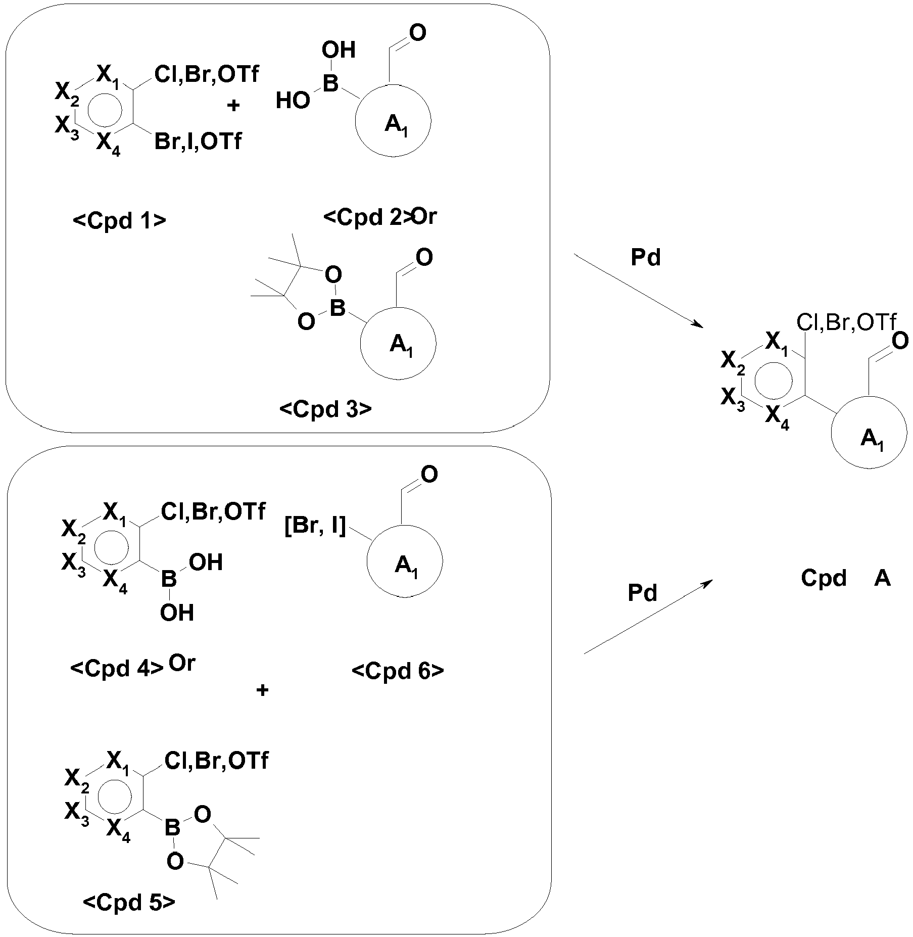
- Specifically, the compound represented by Cpd B may be preapred as described below.
2) an imidazole group may be manufactured through an acid catalyst by mixing Cpd A substituted by the halogen group and the formyl group, a diketo derivative (Cpd 7) having R1 and R2 substituents, and ammonium acetate. Alternatively, the imidazole group may be manufactured through an acid catalyst by mixing Cpd A substituted by the halogen group and the formyl group and a diamine derivative (Cpd 8) having R1 and R2 substituents. - The preparation method may be represented by the following
Reaction Equation 2.
- Specifically, the compound represented by Cpd C (Formula 3-1) may be preapred through
3) a cyclization reaction of Cpd B substituted by the halogen group and the imidazole group by using a Pd catalyst in a molecule. - The preparation method may be represented by the following Reaction Equation 3.

- In addition, compounds having intrinsic properties of the introduced substituent groups may be synthesized by introducing various substituent groups to the aforementioned core structure. For example, it is possible to manufacture a material satisfying conditions required in each organic material layer by introducing the substituent group used in a hole injection layer material, a hole transport layer material, a light emitting layer material and an electron transport layer material used to manufacture the organic light emitting device and the organic electronic device to the aforementioned structure. The compound of the present invention may be applied to the organic electronic device according to a general method of manufacturing the organic electronic device.
- In an exemplary embodiment of the present invention, the organic electronic device may be constituted by a structure comprising a first electrode, a second electrode, and an organic material layer interposed therebetween, and may be manufactured by using the general method of manufacturing the organic electronic device and a general material thereof, except that the compound according to the present invention is used in the organic material layer of the organic electronic device.
- The organic material layer of the organic electronic device of the present invention may be constituted by a single layer structure, but by a multilayered structure in which two or more organic material layers are laminated. For example, the organic electronic device of the present invention may have a structure comprising a hole injection layer, a hole transport layer, a light emitting layer, an electron transport layer, an electron injection layer and the like as an organic material layer. However, the structure of the organic electronic device is not limited thereto, but may comprise the smaller number of organic material layers.
- Accordingly, in the organic electronic device of the present invention, the organic material layer may comprise one or more layers of the hole injection layer, the hole transport layer, and a layer injecting and transporting holes simultaneously, and one or more layers of the layers may comprise the compound represented by Formula 3-1.
- In addition, the organic material layer may comprise the light emitting layer, and the light emitting layer may comprise the compound represented by Formula 3-1. Herein, the compound represented by Formula 3-1 may be comprised as a host material in the light emitting layer. In the case where the compound represented by Formula 3-1 is comprised as the host material in the light emitting layer, the light emitting layer may comprise one or more kinds of phosphorescent dopants.
- In the present invention, the phosphorescent dopant applied to the organic electronic device is not particularly limited, but is preferably selected from the phosphorescent dopant compounds represented by the following
Formula 7.
[Formula 7] M1L10L11L12
InFormula 7, - M1 is Ir or Os,
- L10, L11 and L12 are ligands bonded to M1, and are each independently selected from the following structures,


- The compound represented by
Formula 7 may be preferably selected from the group consisting of the following Structural Formulas, but is not limited thereto.


- The content of the phosphorescent dopant may be 1 to 50 wt% based on the total weight of the material constituting the light emitting layer, but is not limited thereto.
- Further, the organic material layer may comprise one or more layers of an electron transport layer, an electron injection layer, and a layer transporting and injecting electrons simultaneously, and one or more layers of the layers may comprise the compound represented by Formula 3-1. Herein, the layer comprising the compound represented by Formula 3-1 may further comprise alkali metal, an alkali metal compound, alkali earth metal, an alkali earth metal compound or a combination thereof that is an n-type dopant. In the present invention, the n-type dopant applied to the organic electronic device is not particularly limited, and is preferably selected from Li, Na, K, Rb, Cs, Mg, Ca, Sr, Ba, La, Nd, Sm, Eu, Tb, Yb, LiF, Li2O, CsF or the following compounds.


- In the case where the electronic transport layer, the electronic injection layer, the layer transporting and injecting electrons simultanesouly and the like are formed by using the n-type dopant and the compound represented by Formula 3-1, an electronic injection characteristic may be improved to exhibit effects of an increase in efficiency of the device, a reduction in driving voltage, and an increase in stability. It is preferable that the n-type dopant be present at the weight ratio of 1 to 70%.
- In the organic material layer having the multilayered structure, the compound represented by Formula 3-1 may be comprised in a light emitting layer, a layer performing hole injection/hole transport and light emitting simultaneously, a layer performing hole transport and light emitting simultaneously, a layer performing electron transport and light emitting simultaneously or the like.
- For example, the structure of the organic electronic device according to the present invention is illustrated in
FIGS. 1 to 5 . -
FIG. 1 illustrates an organic electronic device having a structure where ananode 2, a hole injection layer 3, ahole transport layer 4, alight emitting layer 5, anelectron transport layer 6 and acathode 7 are sequentially laminated on asubstrate 1. In the aforementioned structure, the compound represented byFormula 1 may be comprised in the hole injection layer 3, thehole transport layer 4, thelight emitting layer 5 or theelectron transport layer 6. -
FIG. 2 illustrates an organic electronic device having a structure where ananode 2, a hole injection layer 3, ahole transport layer 4, alight emitting layer 5, and acathode 7 are sequentially laminated on asubstrate 1. In the aforementioned structure, the compound represented byFormula 1 may be comprised in the hole injection layer 3, thehole transport layer 4, or theelectron transport layer 6. -
FIG. 3 illustrates an organic electronic device having a structure where ananode 2, ahole transport layer 4, alight emitting layer 5, anelectron transport layer 6 and acathode 7 are sequentially laminated on asubstrate 1. In the aforementioned structure, the compound represented byFormula 1 may be comprised in thehole transport layer 4, thelight emitting layer 5 or theelectron transport layer 6. -
FIG. 4 illustrates an organic electronic device having a structure where ananode 2, alight emitting layer 5, anelectron transport layer 6 and acathode 7 are sequentially laminated on asubstrate 1. In the aforementioned structure, the compound represented byFormula 1 may be comprised in thelight emitting layer 5 or theelectron transport layer 6. -
FIG. 5 illustrates an organic electronic device having a structure where ananode 2, alight emitting layer 5 and acathode 7 are sequentially laminated on asubstrate 1. In the aforementioned structure, the compound represented byFormula 1 may be comprised in thelight emitting layer 5. - For example, the organic electronic device according to the present invention may be manufactured by forming an anode by depositing metal or metal oxides having the conductivity or an alloy thereof on a substrate by using a PVD (physical vapor deposition) method such as sputtering or e-beam evaporation, forming the organic material layer comprising the hole injection layer, the hole transport layer, the light emitting layer and the electron transport layer thereon, and depositing the material that is capable of being used as the cathode thereon.
- In addition to this method, the organic electronic device may be manufactured by sequentially depositing a cathode material, an organic material layer and an anode material on a substrate (International Patent Application No.
2003/012890 ). The organic material layer may have a multilayered structure comprising a hole injection layer, a hole transport layer, a light emitting layer, an electron transport layer and the like, but is not limited thereto and may have a single layer structure. Further, the organic material layer may be manufactured in a smaller number of layer by using various polymer materials and by using not a deposition method but a solvent process, for example, a method such as spin coating, dip coating, doctor blading, screen printing, inkjet printing or a heat transferring method. - In general, it is preferable to use the material having a large work function as the anode material so as to smoothly perform hole injection into the organic material layer. Specific examples of the anode material that can be used in the present invention comprise metal such as vanadium, chrome, copper, zinc and gold or an alloy thereof; metal oxides such as zinc oxides, indium oxides, indium tin oxides (ITO) and indium zinc oxides (IZO); a combination of metal and oxides such as ZnO:Al or SnO2:Sb; and conductive polymers such as poly(3-methylthiophene), poly[3,4-(ethylene-1,2-dioxy)thiophene] (PEDT), polypyrrole and polyaniline, but are not limited thereto.
- It is preferable that the cathode material be, in general, a material having a small work function so as to smoothly perform electron injection into the organic material layer. Specific examples of the cathode material include metal such as magnesium, calcium, sodium, potassium, titanium, indium, yttrium, lithium, gadolinium, aluminum, silver, tin and lead or an alloy thereof; a multilayered structure material such as LiF/Al or LiO2/Al and the like, but are not limited thereto.
- The hole injection material is a material that is capable of well receiving holes from the anode at a low voltage, and it is preferable that the HOMO (highest occupied molecular orbital) of the hole injection material be a value between the work function of the anode material and the HOMO of the organic material layer around them. Specific examples of the hole injecting material include metal porphyrin, oligothiophene, an arylamine-based organic material, hexanitrile hexaazatriphenylene, a quinacridone-based organic material, a perylene-based organic material, anthraquinone, polyaniline and polythiophene-based conductive polymers and the like, but are not limited thereto.
- The hole transport material is a material that is capable of receiving the holes from the anode or the hole injection layer and transferring the holes to the light emitting layer, and it is preferable to use the material having large mobility to the holes. Specific examples thereof include an arylamine-based organic material, a conductive polymer, a block copolymer in which a conjugate portion and a non-conjugate portion are present together and the like, but are not limited thereto.
- The light emitting material is a material that receives the holes and the electrons from the hole transport layer and the electron transport layer and combines them to emit light in the range of visible rays, and it is preferable to use the material having excellent photon efficiency to fluorescence or phosphorescence. Specific examples thereof include a 8-hydroxy-quinoline aluminum complex (Alq3); a carbazole-based compound; a dimerized styryl compound; BAlq; 10-hydroxybenzoquinoline-metal compound; a benzoxazole, benzthiazole and benzimidazole-based compound; a poly(p-phenylenevinylene) (PPV)-based polymer; a spiro compound; polyfluorene, lubrene and the like, but are not limited thereto.
- The hole transport material is a material that receives well the electrons from the cathode and transfer the electrons to the light emitting layer, and it is preferable to use the material having large mobility to the electrons. Specific examples thereof include a 8-hydroxyquinoline Al complex; a complex including Alq3; an organic radical compound; a hydroxyflavone metal complex and the like, but are not limited thereto.
- The organic light emitting device according to the present invention may be a top emission type, a bottom emission type, or a both-sided emission type according to the used material.
- The compound according to the present invention may be applied to an organic electronic device such as an organic solar cell, an organic photoconductor and an organic transistor by the principle that is similar to the principle applied to the organic light emitting device.
- Hereinafter, preferable Examples will be described in order to help understanding of the present invention. However, the following Examples are set forth to illustrate the present invention, but the scope of the present invention is not limited thereto.
-


- After 2,4-dichlorophenylboronic acid (18.3 g, 95.8 mmol) and 2-bromo-1-naphthaldehyde (20.5 g, 87.2 mmol) were completely dissolved in tetrahydrofurane (THF) (300 mL), 2M potassium carbonate aqueous solution (180 mL) was added thereto, and tetrakistriphenylphosphino palladium (Pd(PPh3)4 (2.0 g, 2 mol%) was put thereinto, agitated and refluxed for 5 hours. The temperature was lowered to normal temperature, the water layer was removed, and the organic layer was dried by anhydrous magnesium sulfate (MgSO4) and filtered. The filtered solution was concentrated under the reduced pressure, and columned with tetrahydrofurane:hexane = 1:10 to prepare compound A-1 (21.0 g, 80%).
MS: [M+H]+=301 - Compound A-1 (26.2 g, 87.0 mmol) prepared in Preparation Example 1-1 and diaminobenzene (9.4 g, 87.0 mmol) were suspended in dioxane (1,4-dioxane) (200 mL) and acetic acid (AcOH) (20 mL). The obtained mixture was agitated and refluxed for about 6 hours, and cooled to normal temperature. After the mixture was diluted by water (100 mL), the generated solid was filtered, washed by water and ethyl ether to prepare compound A-2 (19.3 g, 57%).
MS: [M+H]+=389 - Compound A-2 (1.99 g, 5.10 mmol) prepared in Preparation Example 1-2, sodium-tertiary-butoxide (NaOt-Bu) (0.58 g, 6.01 mmol) and Pd[P(t-Bu)3]2 (51 mg, 2 mol%) were suspended in toluene (50 mL). The obtained mixture was agitated and refluxed for about 6 hours, and cooled to normal temperature. Distilled water was put into the reaction solution to terminate the reaction, and the organic layer was extracted, dried by anhydrous magnesium sulfate and filtered. The filtered solution was concentrated under the reduced pressure, and columned with tetrahydrofurane:hexane = 1:5 to prepare compound A-3 (0.756 g, 42%).
MS: [M+H]+=353 - Compound A-3 (14.4 g, 40.8 mmol) prepared in Preparation Example 1-3, bis(pinacolato)diboron (11.4 g, 4.49 mmol) and potassium acetate (KOAc) (12.0 g, 122 mmol) were suspended in dioxane (250 mL). Pd(dba)2 (0.70 g, 3 mol%) and PCy3 (0.69 g, 6 mol%) were added to the suspension solution. The mixture was agitated and refluxed for about 8 hours, and cooled to normal temperature. The mixture was diluted by water (250 mL), and extracted by dichloromethane (3 × 150 mL). The organic extract material was dried over magnesium sulfate and then filtered. The filtered solution was concentrated under the reduced pressure, recrystallized by ethyl ether and hexane to prepare compound A-4 (14.5 g, 80%).
MS: [M+H]+ = 445 -


- Compound A-8 was prepared by using the same method as Preparation Example 1, except that 2,5-dichlorophenylboronic acid was used instead of 2,4-dichlorophenyl-boronic acid in Preparation Example 1.
MS: [M+H]+ = 445 -


- Compound A-12 was prepared by using the same method as Preparation Example 1, except that 3-bromo-2-naphthaldehyde was used instead of 2-bromo-1-naphthaldehyde in Preparation Example 1.
MS: [M+H]+ = 445 -


- Compound A-16 was prepared by using the same method as Preparation Example 1, except that 2,5-dichlorophenylboronic acid was used instead of 2,4-dichlorophenylboronic acid and 3-bromo-2-naphthaldehyde was used instead of 2-bromo-1-naphthaldehyde in Preparation Example 1.
MS: [M+H]+ = 445 -


- Compound A-20 was prepared by using the same method as Preparation Example 1, except that 1-bromo-2-naphthaldehyde was used instead of 2-bromo-1-naphthaldehyde in Preparation Example 1.
MS: [M+H]+ = 445 -


- Compound A-24 was prepared by using the same method as Preparation Example 1, except that 2,5-dichlorophenylboronic acid was used instead of 2,4-dichlorophenylboronic acid and 1-bromo-2-naphthaldehyde was used instead of 2-bromo-1-naphthaldehyde in Preparation Example 1.
MS: [M+H]+ = 445 -


- Compound A-28 was prepared by using the same method as Preparation Example 1, except that 2-chloro-3-quinolinecarboxaldehyde was used instead of 2-bromo-1-naphthaldehyde in Preparation Example 1.
MS: [M+H]+ = 446 -


- Compound A-32 was prepared by using the same method as Preparation Example 1, except that 2,5-dichlorophenylboronic acid was used instead of 2,4-dichlorophenylboronic acid and 2-chloro-3-quinolinecarboxaldehyde was used instead of 2-bromo-1-naphthaldehyde in Preparation Example 1.
MS: [M+H]+ = 446 -


- Compound A-35 was prepared by using the same method as Preparation Example 1, except that ammonium acetate and benzil were used instead of diaminobenzene in Preparation Example 1.
MS: [M+H]+ = 547 -


- Compound A-38 was prepared by using the same method as Preparation Example 1, except that diaminonaphthalene was used instead of diaminobenzene in Preparation Example 1.
MS: [M+H]+ = 495 -


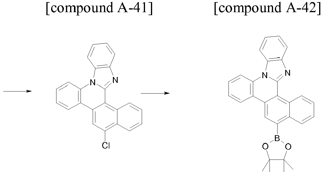
- After 2-chlorophenylboronic acid (17.2 g, 110 mmol) and 2-bromo-4-chloro-1-naphthaldehyde (26.9 g, 100 mmol) were completely dissolved in tetrahydrofurane (THF) (300 mL), 2M potassium carbonate aqueous solution (180 mL) was added thereto, and tetrakistriphenylphosphino palladium (Pd(PPh3)4 (2.3 g, 2 mol%) was put thereinto, agitated and refluxed for 5 hours. The temperature was lowered to normal temperature, the water layer was removed, and the organic layer was dried by anhydrous magnesium sulfate (MgSO4) and filtered. The filtered solution was concentrated under the reduced pressure, and columned with tetrahydrofurane:hexane = 1:10 to prepare compound A-39 (22.8 g, 76%).
MS: [M+H]+=301 - Compound A-40 was prepared by using the same method as Preparation Example 1-2, except that compound A-39 was used instead of compound A-1 in Preparation Example 1-2.
MS: [M+H]+=389 - Compound A-41 was prepared by using the same method as Preparation Example 1-3, except that compound A-40 was used instead of compound A-2 in Preparation Example 1-3.
MS: [M+H]+=353 - Compound A-42 was prepared by using the same method as Preparation Example 1-3, except that compound A-41 was used instead of compound A-3 in Preparation Example 1-4.
MS: [M+H]+=445 -


- Compound A-46 was prepared by using the same method as Preparation Example 1, except that 8-bromo-7-quinolinecarboxaldehyde was used instead of 2-bromo-1-naphthaldehyde in Preparation Example 1.
MS: [M+H]+ = 446 -


- Compound A-50 was prepared by using the same method as Preparation Example 11, except that 2,3-dichloropyridine was used instead of 2-chlorophenyl-boronic acid and 4-chloro-1-formyl-2-naphthalene-2-boronic acid was used instead of 2-bromo-4-chloro-1-naphthaldehyde in Preparation Example 11.
MS: [M+H]+ = 446 -
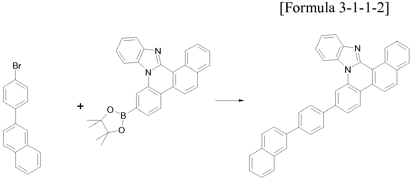
- After 2-(4-bromophenyl)naphthalene (2.83 g, 10.0 mmol) and compound A-4 (4.44 g, 10.0 mmol) were dissolved in tetrahydrofurane (100 mL), 2M potassium carbonate aqueous solution (20 mL) was added thereto, and tetrakistriphenylphosphino palladium (231 mg, 2 mol%) was put thereinto, agitated and refluxed for 5 hours. The temperature was lowered to normal temperature, and the generated solid was filtered. The filtered solid was recrystallized by chloroform and ethanol, filtered, and dried to prepare the compound of Formula 3-1-1-2 (3.54 g, 68%).
MS: [M+H]+ = 521 -

- Formula 3-1-1-6 was prepared by using the same method as Example 1, except that compound B-1 was used instead of 2-(4-bromophenyl)naphthalene in Example 1.
MS: [M+H]+ = 637 -

- Formula 3-1-1-7 was prepared by using the same method as Example 1, except that compound B-2 was used instead of 2-(4-bromophenyl)naphthalene in Example 1.
MS: [M+H]+ = 621 -

- Formula 3-1-1-12 was prepared by using the same method as Example 1, except that compound B-3 was used instead of 2-(4-bromophenyl)naphthalene in Example 1.
MS: [M+H]+ = 587 -

- Formula 3-1-1-24 was prepared by using the same method as Example 1, except that compound B-4 was used instead of 2-(4-bromophenyl)naphthalene in Example 1.
MS: [M+H]+ = 595 -


- After 2-(4-bromophenyl)naphthalene (2.83 g, 10.0 mmol) and compound A-8 (4.44 g, 10.0 mmol) were dissolved in tetrahydrofurane (100 mL), 2M potassium carbonate aqueous solution (20 mL) was added thereto, and tetrakistriphenylphosphino palladium (231 mg, 2 mol%) was put thereinto, agitated and refluxed for 5 hours. The temperature was lowered to normal temperature, and the generated solid was filtered. The filtered solid was recrystallized by chloroform and ethanol, filtered, and dried to prepare the compound of Formula 3-1-2-2 (3.75 g, 72%).
MS: [M+H]+ = 521 -

- Formula 3-1-2-15 was prepared by using the same method as Example 6, except that compound C-1 was used instead of 2-(4-bromophenyl)naphthalene in Example 6.
MS: [M+H]+ = 676 -

- Formula 3-1-2-21 was prepared by using the same method as Example 6, except that compound C-2 was used instead of 2-(4-bromophenyl)naphthalene in Example 6.
MS: [M+H]+ = 621 -

- After 2-(4-bromophenyl)naphthalene (2.83 g, 10.0 mmol) and compound A-12 (4.44 g, 10.0 mmol) were dissolved in tetrahydrofurane (100 mL), 2M potassium carbonate aqueous solution (20 mL) was added thereto, and tetrakistriphenylphosphino palladium (231 mg, 2 mol%) was put thereinto, agitated and refluxed for 5 hours. The temperature was lowered to normal temperature, and the generated solid was filtered. The filtered solid was recrystallized by chloroform and ethanol, filtered, and dried to prepare the compound of Formula 3-2-1-2 (2.76 g, 53%).
MS: [M+H]+ = 521 -

- Formula 3-2-1-11 was prepared by using the same method as Reference Example 9, except that compound D-1 was used instead of 2-(4-bromophenyl)naphthalene in Reference Example 9.
MS: [M+H]+ = 511 -

- After 2-(4-bromophenyl)naphthalene (2.83 g, 10.0 mmol) and compound A-16 (4.44 g, 10.0 mmol) were dissolved in tetrahydrofurane (100 mL), 2M potassium carbonate aqueous solution (20 mL) was added thereto, and tetrakistriphenylphosphino palladium (231 mg, 2 mol%) was put thereinto, agitated and refluxed for 5 hours. The temperature was lowered to normal temperature, and the generated solid was filtered. The filtered solid was recrystallized by chloroform and ethanol, filtered, and dried to prepare the compound of Formula 3-2-2-2 (3.13 g, 60%).
MS: [M+H]+ = 521 -

- Formula 3-2-2-14 was prepared by using the same method as Reference Example 11, except that compound E-1 was used instead of 2-(4-bromophenyl)naphthalene in Reference Example 11.
MS: [M+H]+ = 725 -

- After 2-(4-bromophenyl)naphthalene (2.83 g, 10.0 mmol) and compound A-20 (4.44 g, 10.0 mmol) were dissolved in tetrahydrofurane (100 mL), 2M potassium carbonate aqueous solution (20 mL) was added thereto, and tetrakistriphenylphosphino palladium (231 mg, 2 mol%) was put thereinto, agitated and refluxed for 5 hours. The temperature was lowered to normal temperature, and the generated solid was filtered. The filtered solid was recrystallized by chloroform and ethanol, filtered, and dried to prepare the compound of Formula 3-3-1-2 (3.80 g, 73%).
MS: [M+H]+ = 521 -

- Formula 3-3-1-18 was prepared by using the same method as Reference Example 13, except that compound F-1 was used instead of 2-(4-bromophenyl)naphthalene in Reference Example 13.
MS: [M+H]+ = 577 -

- After 2-(4-bromophenyl)naphthalene (2.83 g, 10.0 mmol) and compound A-24 (4.44 g, 10.0 mmol) were dissolved in tetrahydrofurane (100 mL), 2M potassium carbonate aqueous solution (20 mL) was added thereto, and tetrakistriphenylphosphino palladium (231 mg, 2 mol%) was put thereinto, agitated and refluxed for 5 hours. The temperature was lowered to normal temperature, and the generated solid was filtered. The filtered solid was recrystallized by chloroform and ethanol, filtered, and dried to prepare the compound of Formula 3-3-2-2 (3.39 g, 65%).
MS: [M+H]+ = 521 -

- Formula 3-8-1-2 was prepared by using the same method as Example 1, except that compound A-28 was used instead of compound A-4 in Example 1.
MS: [M+H]+ = 522 -

- Formula 3-8-2-2 was prepared by using the same method as Example 1, except that compound A-32 was used instead of compound A-4 in Example 1.
MS: [M+H]+ = 522 -


- Formula 3-1-1-29 was prepared by using the same method as Example 1, except that 4-bromobiphenyl was used instead of 2-(4-bromophenyl)naphthalene in Example 1.
MS: [M+H]+ = 471 -

- Formula 3-1-1-30 was prepared by using the same method as Example 1, except that compound F-2 was used instead of 2-(4-bromophenyl)naphthalene in Example 1.
MS: [M+H]+ = 587 -

- Formula 3-1-1-33 was prepared by using the same method as Example 1, except that compound F-3 was used instead of 2-(4-bromophenyl)naphthalene in Example 1.
MS: [M+H]+ = 547 -

- Formula 3-1-2-14 was prepared by using the same method as Example 6, except that compound E-1 was used instead of 2-(4-bromophenyl)naphthalene in Example 6.
MS: [M+H]+ = 725 -

- Formula 3-1-2-29 was prepared by using the same method as Example 6, except that 3-bromophenanthrene was used instead of 2-(4-bromophenyl)naphthalene in Example 6.
MS: [M+H]+ = 495 -


- Formula 3-1-2-30 was prepared by using the same method as Example 6, except that 2-bromophenanthrene was used instead of 2-(4-bromophenyl)naphthalene in Example 6.
MS: [M+H]+ = 495 -

- Formula 3-1-2-33 was prepared by using the same method as Example 6, except that compound F-4 was used instead of 2-(4-bromophenyl)naphthalene in Example 6.
MS: [M+H]+ = 560 -

- Formula 3-2-1-23 was prepared by using the same method as Reference Example 9, except that compound F-5 was used instead of 2-(4-bromophenyl)naphthalene in Reference Example 9.
MS: [M+H]+ = 626 -

- Formula 3-3-2-28 was prepared by using the same method as Reference Example 15, except that compound F-6 was used instead of 2-(4-bromophenyl)naphthalene in Reference Example 15.
MS: [M+H]+ = 595 -
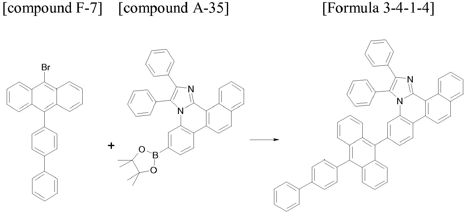
- After compound F-7 (4.09 g, 10.0 mmol) and compound A-35 (5.46 g, 10.0 mmol) were dissolved in tetrahydrofurane (100 mL), 2M potassium carbonate aqueous solution (20 mL) was added thereto, and tetrakistriphenylphosphino palladium (231 mg, 2 mol%) was put thereinto, agitated and refluxed for 5 hours. The temperature was lowered to normal temperature, and the generated solid was filtered. The filtered solid was recrystallized by chloroform and ethanol, filtered, and dried to prepare the compound of Formula 3-4-1-4 (5.31 g, 71%).
MS: [M+H]+ = 749 -

- Formula 3-4-1-6 was prepared by using the same method as Reference Example 27, except that compound F-8 was used instead of compound F-7 in Reference Example 27.
MS: [M+H]+ = 663 -

- After 4-bromobiphenyl (2.33 g, 10.0 mmol) and compound A-38 (4.94 g, 10.0 mmol) were dissolved in tetrahydrofurane (100 mL), 2M potassium carbonate aqueous solution (20 mL) was added thereto, and tetrakistriphenylphosphino palladium (231 mg, 2 mol%) was put thereinto, agitated and refluxed for 5 hours. The temperature was lowered to normal temperature, and the generated solid was filtered. The filtered solid was recrystallized by chloroform and ethanol, filtered, and dried to prepare the compound of Formula 3-5-1-1 (3.85 g, 74%).
MS: [M+H]+ = 521 -

- Formula 3-5-1-7 was prepared by using the same method as Reference Example 29, except that compound F-9 was used instead of 4-bromobiphenyl in Reference Example 29.
MS: [M+H]+ = 548 -


- After 4-bromobiphenyl (2.33 g, 10.0 mmol) and compound A-42 (4.44 g, 10.0 mmol) were dissolved in tetrahydrofurane (100 mL), 2M potassium carbonate aqueous solution (20 mL) was added thereto, and tetrakistriphenylphosphino palladium (231 mg, 2 mol%) was put thereinto, agitated and refluxed for 5 hours. The temperature was lowered to normal temperature, and the generated solid was filtered. The filtered solid was recrystallized by chloroform and ethanol, filtered, and dried to prepare the compound of Formula 3-6-1-1 (3.05 g, 65%).
MS: [M+H]+ = 471 -

- Formula 3-6-1-4 was prepared by using the same method as Reference Example 31, except that compound F-10 was used instead of 4-bromobiphenyl in Reference Example 31.
MS: [M+H]+ = 610 -


- After compound F-11 (3.83 g, 10.0 mmol) and compound A-50 (4.45 g, 10.0 mmol) were dissolved in tetrahydrofurane (100 mL), 2M potassium carbonate aqueous solution (20 mL) was added thereto, and tetrakistriphenylphosphino palladium (231 mg, 2 mol%) was put thereinto, agitated and refluxed for 5 hours. The temperature was lowered to normal temperature, and the generated solid was filtered. The filtered solid was recrystallized by chloroform and ethanol, filtered, and dried to prepare the compound of Formula 3-6-2-7 (4.04 g, 65%).
MS: [M+H]+ = 622 -

- Formula 3-6-2-9 was prepared by using the same method as Reference Example 33, except that compound F-12 was used instead of compound F-11 in Reference Example 33.
MS: [M+H]+ = 562 -


- Compound F-13 (6.71 g, 20.2 mmol) and compound A-31 (7.13 g, 20.2 mmol) were dispersed in xylene (150 mL), and NaOt-Bu (2.9 g, 30.3 mmol) and Pd[P(t-Bu)3]2 (0.1 g, 0.20 mmol) were added thereto, agitated and refluxed for 5 hours. The temperature was lowered to normal temperature, and the generated solid was filtered. The filtered solid was recrystallized by chloroform and ethanol, filtered, and dried to prepare the compound of Formula 3-8-2-16 (6.69 g, 51%).
MS: [M+H]+ = 650 -

- After compound F-14 (3.22 g, 10.0 mmol) and compound A-46 (4.45 g, 10.0 mmol) were dissolved in tetrahydrofurane (100 mL), 2M potassium carbonate aqueous solution (20 mL) was added thereto, and tetrakistriphenylphosphino palladium (231 mg, 2 mol%) was put thereinto, agitated and refluxed for 5 hours. The temperature was lowered to normal temperature, and the generated solid was filtered. The filtered solid was recrystallized by chloroform and ethanol, filtered, and dried to prepare the compound of Formula 3-9-1-11 (3.47 g, 62%).
MS: [M+H]+ = 561 -

- Formula 3-9-1-13 was prepared by using the same method as Reference Example 36, except that compound F-15 was used instead of compound F-14 in Reference Example 36.
MS: [M+H]+ = 611 -

- Formula 3-1-1-34 was prepared by using the same method as Example 1, except that compound F-16 was used instead of 2-(4-bromophenyl)naphthalene in Example 1.
MS: [M+H]+ = 476 - A glass substrate on which a thin film of indium tin oxide (ITO) was applied to a thickness of 500 Å was immersed in distilled water having a detergent dissolved therein and washed by the ultrasonic wave. In this case, the used detergent was a product commercially available from Fisher Co. and the distilled water was one which had been twice filtered by using a filter commercially available from Millipore Co. ITO was washed for 30 minutes, and then washing with ultrasonic waves was repeated twice for 10 minutes by distilled water. After washing with distilled water was finished, washing with ultrasonic waves was performed by using solvents such as isopropyl alcohol, acetone and methanol, and the resultant product was dried and transported to the plasma washing machine. In addition, the substrate was washed by using the oxygen plasma for 5 minutes, and then transported to the vacuum deposition machine.
- Hexanitrile hexaazatriphenylene (HAT) of the following Formula was applied to thicknesses of 500 Å by thermal vacuum deposition on the ITO transparent electrode thus prepared to form a hole injecting layer.

- 4,4'-bis[N-(1-naphthyl)-N-phenylamino]biphenyl (NPB) (250 Å), hexanitrile hexaazatriphenylene (HAT) (50 Å) and 4,4'-bis[N-(1-naphthyl)-N-phenylamino]biphenyl (NPB) (400 Å) of the aforementioned Formulas were sequentially vacuum deposited on the hole injection layer to form the hole transport layer.
- Subsequently, GH and GD shown below were vacuum deposited at a weight ratio of 20:1 on the hole transport layer to form the light emitting layer in a film thickness of 300 Å.

- The compound of Formula 3-1-1-2 prepared in Example 1 and the following Formula LiQ (lithium quinalate) were vacuum deposited at a weight ratio of 1:1 on the light emitting layer to form the electronic injection and transport layer in a thickness of 200 Å.

- Lithium fluoride (LiF) in a thickness of 15 Å and aluminum in a thickness of 1,000 Å were subsequently deposited on the electron injection and transport layer to form the cathode.
- In the aforementioned process, the deposition speed of the organic material was maintained at 0.4 to 0.7 Å/sec, the deposition speed of lithium fluoride of the cathode was maintained at 0.3 Å/sec, the deposition speed of aluminum was maintained at 2 Å/sec, and the degree of vacuum during deposition was maintained at 2 × 10⁻⁷ to 5 × 10⁻⁸ torr to manufacture the organic light emitting device.
- The organic light emitting device was manufactured by using the same method as Experimental Example 1-1-1, except that the following compound of Formula ET-A was used instead of the compound of Formula 3-1-1-2 in Experimental Example 1-1-1.

- The organic light emitting device was manufactured by using the same method as Experimental Example 1-1-1, except that the following compound of Formula ET-B was used instead of the compound of Formula 3-1-1-2 in Experimental Example 1-1-1.

- The organic light emitting device was manufactured by using the same method as Experimental Example 1-1-1, except that each compound shown in Table 1 was used instead of the compound of Formula 3-1-1-2 in Experimental Example 1-1-1.
- When the current (10 mA/cm2) was applied to the organic light emitting devices manufactured in Experimental Examples 1-1-1 and 1-1-4 to 1-1-10, Reference Experimental Examples 1-1-3 and 1-1-11 to 1-1-21, and Comparative Examples 1 and 2, the results of Table 1 were obtained.
[Table 1] Compound Voltage (V) Efficiency (cd/A) Color coordinate (x, y) Experimental Example 1-1-1 3-1-1-2 4.14 31.24 (0.314, 0.650) Experimental Example 1-1-2 3-1-1-6 4.01 32.01 (0.314, 0.649) Reference Experimental Example 1-1-3 3-1-1-7 3.71 33.53 (0.314, 0.650) Experimental Example 1-1-4 3-1-1-12 4.05 30.10 (0.313, 0.650) Experimental Example 1-1-5 3-1-1-24 4.40 29.95 (0.315, 0.650) Experimental Example 1-1-6 3-1-1-29 4.09 32.57 (0.314, 0.650) Experimental Example 1-1-7 3-1-1-30 4.05 32.87 (0.315, 0.649) Experimental Example 1-1-8 3-1-1-33 3.85 32.23 (0.314, 0.650) Experimental Example 1-1-9 3-1-1-34 4.07 32.47 (0.314, 0.650) Experimental Example 1-1-10 3-1-2-2 4.53 30.95 (0.314, 0.649) Reference Experimental Example 1-1-11 3-2-1-2 3.92 32.88 (0.313, 0.649) Reference Experimental Example 1-1-12 3-2-1-11 4.30 29.15 (0.314, 0.651) Reference Experimental Example 1-1-13 3-2-1-23 4.02 31.57 (0.315, 0.648) Reference Experimental Example 1-1-14 3-2-2-14 4.28 28.31 (0.315, 0.650) Reference Experimental Example 1-1-15 3-3-1-2 3.83 32.50 (0.314, 0.650) Reference Experimental Example 1-1-16 3-3-1-18 4.45 29.87 (0.315, 0.651) Reference Experimental Example 1-1-17 3-4-1-4 3.92 32.20 (0.314, 0.650) Reference Experimental Example 1-1-18 3-5-1-1 4.01 32.06 (0.315, 0.649) Reference Experimental Example 1-1-19 3-6-1-1 3.95 31.84 (0.314, 0.651) Reference Experimental Example 1-1-20 3-8-1-2 4.51 27.95 (0.314, 0.651) Reference Experimental Example 1-1-21 3-8-2-2 4.25 29.33 (0.315, 0.649) Comparative Example 1 ET-A 4.36 28.66 (0.315, 0.650) Comparative Example 2 ET-B 4.29 27.98 (0.314, 0.650) - From the results of Table 1, it can be seen that the new compound according to the present invention may be used as a material of an organic material layer of an organic electronic device comprising an organic light emitting device, and the organic electronic device comprising the organic light emitting device using the same exhibits excellent properties in views of efficiency, driving voltage, stability and the like. In particular, the new compound according to the present invention has excellent thermal stability, a deep HOMO level, a high triplet state and hole stability, thus exhibiting excellent properties. The compound may be used alone in the organic electronic device comprising the organic light emitting device, or may be used while being mixed with the n-type dopant such as LiQ. The new compound according to the present invention may improve efficiency and stability of the device by thermal stability of the compound.
- Hexanitrile hexaazatriphenylene (HAT) of the aforementioned Formula was applied to thicknesses of 100 Å by thermal vacuum deposition on the ITO transparent electrode prepared in Experimental Example 1-1-1 to form a hole injecting layer.
- 4,4'-bis[N-(1-naphthyl)-N-phenylamino]biphenyl (NPB) (700 Å), hexanitrile hexaazatriphenylene (HAT) (50 Å) and 4,4'-bis[N-(1-naphthyl)-N-phenylamino]biphenyl (NPB) (700 Å) of the aforementioned Formulas were sequentially applied by vacuum deposition on the hole injection layer to form a hole transport layer.
- Subsequently, BH and BD shown below were applied by vacuum deposition at a weight ratio of 25:1 on the hole transport layer to form a light emitting layer in a film thickness of 200 Å.
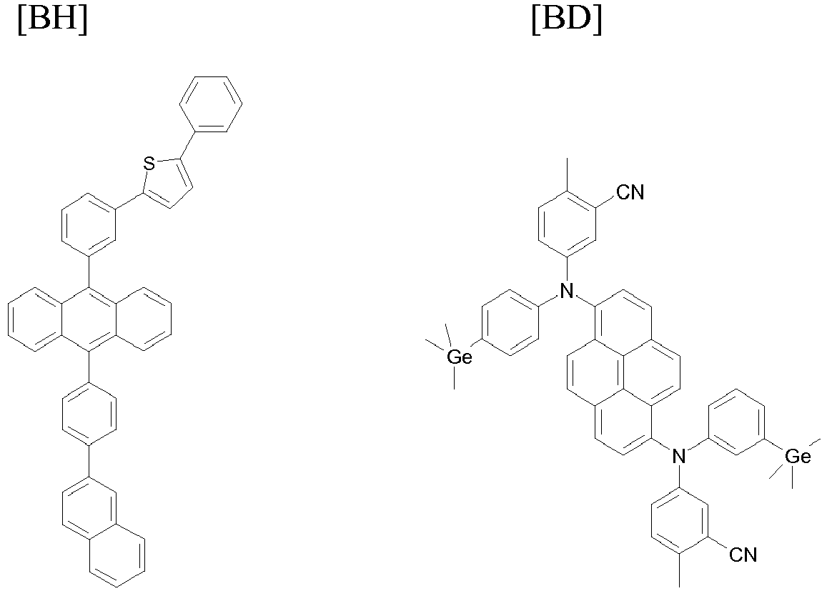
- The compound of Formula 3-1-2-2 (200 Å) prepared in Example 11 and the compound of ET-A (100 Å) were sequentially applied by vacuum deposition on the light emitting layer to form an electronic injection and transport layer.
- Lithium fluoride (LiF) in a thickness of 15 Å and aluminum in a thickness of 1,000 Å were subsequently deposited on the electron injection and transport layer to form a cathode.
- In the aforementioned process, the deposition speed of the organic material was maintained at 0.4 to 0.7 Å/sec, the deposition speed of lithium fluoride of the cathode was maintained at 0.3 Å/sec, the deposition speed of aluminum was maintained at 2 Å/sec, and the degree of vacuum during deposition was maintained at 2 × 10⁻⁷ to 5 × 10⁻⁸ torr to manufacture the organic light emitting device.
- The organic light emitting device was manufactured by using the same method as Experimental Example 2-1-1, except that the following compound of Formula ET-C was used instead of the compound of Formula 3-1-2-2 in Experimental Example 2-1-1.

- The organic light emitting device was manufactured by using the same method as Experimental Example 2-1-1, except that each compound shown in Table 2 was used instead of the compound of Formula 3-1-2-2 in Experimental Example 2-1-1.
- When the current (10 mA/cm2) was applied to the organic light emitting devices manufactured in Experimental Examples 2-1-1 to 2-1-4, Reference Experimental Examples 2-1-5 to 2-1-12, and Comparative Example 3, the results of Table 2 were obtained.
[Table 2] Compound Voltage (V) Efficiency (cd/A) Color coordinate (x, y) Experimental Example 2-1-1 3-1-2-2 4.17 5.79 (0.134, 0.159) Experimental Example 2-1-2 3-1-2-21 4.23 5.89 (0.134, 0.160) Experimental Example 2-1-3 3-1-2-29 4.30 5.62 (0.134, 0.158) Experimental Example 2-1-4 3-1-2-30 4.02 5.95 (0.135, 0.161) Reference 3-1-2-33 4.15 6.02 (0.134, 0.160) Experimental Example 2-1-5 Reference Experimental Example 2-1-6 3-2-2-2 4.25 5.91 (0.136, 0.162) Reference Experimental Example 2-1-7 3-3-2-2 4.17 5.72 (0.134, 0.159) Reference Experimental Example 2-1-8 3-3-2-28 4.21 5.95 (0.135, 0.160) Reference Experimental Example 2-1-9 3-4-1-6 4.09 5.86 (0.134, 0.159) Reference Experimental Example 2-1-10 3-5-1-7 4.41 5.74 (0.135, 0.160) Reference Experimental Example 2-1-11 3-6-2-9 4.42 6.15 (0.135, 0.161) Reference Experimental Example 2-1-12 3-9-1-11 4.19 5.78 (0.134, 0.160) Comparative Example 3 ET-C 4.82 3.26 (0.135, 0.162) - From the results of Table 2, it can be seen that the new compound according to the present invention may be used as a material of an organic material layer of an organic electronic device comprising an organic light emitting device, and the organic electronic device comprising the organic light emitting device using the same exhibits excellent properties in views of efficiency, driving voltage, stability and the like. Particularly, the new compound according to the present invention had excellent hole blocking and electron transporting abilities, thus exhibiting high efficiency properties.
- Hexanitrile hexaazatriphenylene (HAT) of the aforementioned Formula was applied to thicknesses of 100 Å by thermal vacuum deposition on the ITO transparent electrode prepared in Experimental Example 1-1-1 to form a hole injecting layer.
- 4,4'-bis[N-(1-naphthyl)-N-phenylamino]biphenyl (NPB) (800 Å) of the aforementioned Formula was applied by vacuum deposition on the hole injection layer to form a hole transport layer.
- Subsequently, the compound of Formula 3-1-2-14 prepared in Reference Example 21 and the dopant compound RD shown below were applied by vacuum deposition at a weight ratio of 10:1 on the hole transport layer to form a light emitting layer in a film thickness of 300 Å.

- The compound of Formula ET-A and the aforementioned Formula LiQ (lithium quinalate) were applied at a weight ratio of 1:1 by vacuum deposition on the light emitting layer to form an electronic injection and transport layer in a thickness of 300 Å.
- Lithium fluoride (LiF) in a thickness of 15 Å and aluminum in a thickness of 1,000 Å were subsequently deposited on the electron injection and transport layer to form a cathode.
- In the aforementioned process, the deposition speed of the organic material was maintained at 0.4 to 0.7 Å/sec, the deposition speed of lithium fluoride of the cathode was maintained at 0.3 Å/sec, the deposition speed of aluminum was maintained at 2 Å/sec, and the degree of vacuum during deposition was maintained at 2 × 10⁻⁷ to 5 × 10⁻⁸ torr to manufacture an organic light emitting device.
- The organic light emitting device was manufactured by using the same method as Reference Experimental Example 3-1-1, except that the following compound of Formula RH-A was used instead of the compound of Formula 3-1-2-14 in Reference Experimental Example 3-1-1.

- The organic light emitting device was manufactured by using the same method as Reference Experimental Example 3-1-1, except that each compound shown in Table 3 was used instead of the compound of Formula 3-1-2-14 in Reference Experimental Example 3-1-1.
- When the current (10 mA/cm2) was applied to the organic light emitting devices manufactured in Experimental Example 3-1-1, Reference Examples 3-1-3 to 3-1-8, and Comparative Example 4, the results of Table 3 were obtained.
[Table 3] Compound Voltage (V) Efficiency (cd/A) Color coordinate (x, y) Reference Experimental Example 3-1-1 3-1-2-14 4.73 17.52 (0.671, 0.329) Experimental Example 3-1-2 3-1-2-15 4.82 16.32 (0.670, 0.330) Reference Experimental Example 3-1-3 3-2-2-14 4.65 18.96 (0.671, 0.331) Reference Experimental Example 3-1-4 3-4-1-6 4.89 15.32 (0.672, 0.330) Reference Experimental Example 3-1-5 3-6-1-4 4.82 18.23 (0.671, 0.332) Reference Experimental Example 3-1-6 3-6-2-7 4.98 19.32 (0.670, 0.331) Reference Experimental Example 3-1-7 3-8-2-16 4.75 16.21 (0.669, 0.330) Reference Experimental Example 3-1-8 3-9-1-13 4.86 19.21 (0.671, 0.331) Comparative Example 3 RH-A 6.12 12.26 (0.672, 0.329) - From the results of Table 3, it can be seen that the new compound according to the present invention may be used as a material of a light emitting layer of an organic electronic device comprising an organic light emitting device, and the organic electronic device comprising the organic light emitting device using the same exhibits excellent properties in views of efficiency, driving voltage, stability and the like. Particularly, the compound may reduce driving voltage and introduce an increase in efficiency to improve power consumption.
Claims (10)
- A compound represented by Formula 3-1:
 R1a to R4a, R3, R6 and R9 to R14 are hydrogen,R4 and R5 are each independently -(L2)r-(Y2)s, where r is an integer of 0 to 10 and s is an integer of 1 to 10,L2 is an arylene group selected from a phenylene group or a naphthalene group,Y2 is hydrogen; heavy hydrogen; a substituted or unsubstituted arylamine group; a substituted or unsubstituted aryl group selected from a phenyl group, a biphenyl group, a terphenyl group, a phenanthrenyl group, a pyrenyl group, a fluorenyl group, a triphenylene group, or a fluoranthrene group; or a substituted or unsubstituted heterocyclic group comprising one or more of N, O and S atoms selected from a pyridyl group, a triazine group, a benzoxazole group, a benzimidazole group, a benzthiazol group, a benzcarbazole group, a dibenzothiophene group, or a dibenzofuranyl group.the term "substituted or unsubstituted" means that a matter is substituted or unsubstituted by at least one substituent group selected from heavy hydrogen; an alkyl group; an arylamine group; an aryl group selected from a phenyl group, a biphenyl group, a terphenyl group, a naphthyl group; and a fluorenyl group.
 - The compound of claim 1, wherein the arylene group is a phenylene group, and the aryl group is a phenyl group, a phenanthrenyl group, a fluorene group, a dimethylfluorene group, a triphenylene group, a benzocrycene group or a fluoranthrene group.
- The compound of claim 1, wherein the compound is any one selected from the group consisting of the following Structural Formulas:
[Formula 3-1-1-1] [Formula 3-1-1-2] [Formula 3-1-1-3] [Formula 3-1-1-4] 

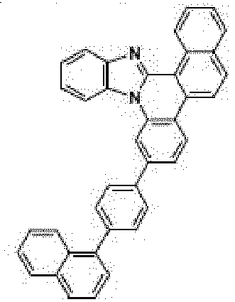

[Formula 3-1-1-5] [Formula 3-1-1-6] [Formula 3-1-1-9] [Formula 3-1-1-10] 


[Formula 3-1-1-11] [Formula 3-1-1-12] [Formula 3-1-1-15] [Formula 3-1-1-16] 


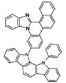
[Formula 3-1-1-18] [Formula 3-1-1-19] [Formula 3-1-1-20] [Formula 3-1-1-21] 


[Formula 3-1-1-23] [Formula 3-1-1-25] 

[Formula 3-1-1-27] [Formula 3-1-1-29] 
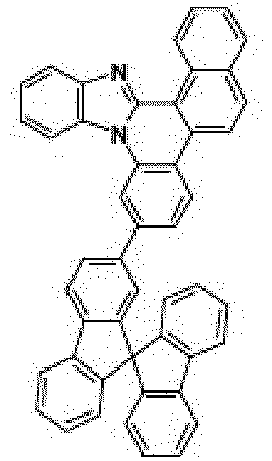


[Formula 3-1-1-30] [Formula 3-1-1-31] [Formula 3-1-1-32] [Formula 3-1-1-33] 


[Formula 3-1-1-34] [Formula 3-1-1-35] [Formula 3-1-1-36] [Formula 3-1-2-1] 
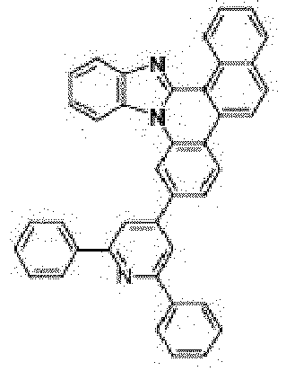


[Formula 3-1-2-2] [Formula 3-1-2-3] [Formula 3-1-2-4] [Formula 3-1-2-5] 


[Formula 3-1-2-6] [Formula 3-1-2-9] [Formula 3-1-2-10] [Formula 3-1-2-11] 


[Formula 3-1-2-12] [Formula 3-1-2-15] [Formula 3-1-2-16] [Formula 3-1-2-18] 


[Formula 3-1-2-19] [Formula 3-1-2-20] [Formula 3-1-2-21] 


[Formula 3-1-2-23] [Formula 3-1-2-25] [Formula 3-1-2-26] 


[Formula 3-1-2-27] [Formula 3-1-2-28] [Formula 3-1-2-29] [Formula 3-1-2-30] 


[Formula 3-1-2-31] [Formula 3-1-2-32] [Formula 3-1-2-34] [Formula 3-1-2-35] 


[Formula 3-1-2-36] 
- An organic electronic device comprising:a first electrode;a second electrode; andone or more organic material layers interposed between the first electrode and the second electrode,wherein one or more layers of the organic material layers comprise the compound of any one of claims 1 to 3.
- The organic electronic device of claim 4, wherein the organic material layer comprises one or more layers of a hole injection layer, a hole transport layer, and a layer injecting and transporting holes simultaneously, and one or more layers of the layers comprise a compound of any one of claims 1 to 3.
- The organic electronic device of claim 4, wherein the organic material layer comprises a light emitting layer, and the light emitting layer comprises a compound of any one of claims 1 to 3.
- The organic electronic device of claim 6, wherein the compound of any one of claims 1 to 3 is comprised as a host material in the light emitting layer, and the light emitting layer further comprises a dopant compound represented by the following Formula 7:
[Formula 7] M1L10L11L12
wherein,M1 is Ir or Os,L10, L11 and L12 are ligands bonded to M1, and are each independently selected from the following structures,

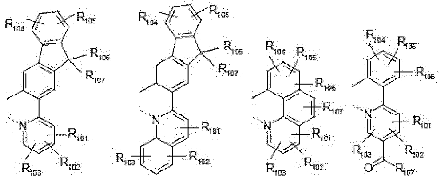
- The organic electronic device of claim 4, wherein the organic material layer comprises one or more layers of an electron transport layer, an electron injection layer, and a layer transporting and injecting electrons simultaneously, and one or more layers of the layers comprise the compound of any one of claims 1 to 3.
- The organic electronic device of claim 8, wherein the organic material layer comprising the compound of any one of claims 1 to 3 further comprises alkali metal, an alkali metal compound, alkali earth metal, an alkali earth metal compound or a combination thereof.
- The organic electronic device of claim 4, wherein the organic electronic device is selected from the group consisting of an organic light emitting device, an organic solar cell, an organic photoconductor (OPC) and an organic transistor.
Applications Claiming Priority (2)
| Application Number | Priority Date | Filing Date | Title |
|---|---|---|---|
| KR20110067965 | 2011-07-08 | ||
| PCT/KR2012/004864 WO2013009013A2 (en) | 2011-07-08 | 2012-06-20 | Novel compound and organic electronic device using same |
Publications (3)
| Publication Number | Publication Date |
|---|---|
| EP2730634A2 EP2730634A2 (en) | 2014-05-14 |
| EP2730634A4 EP2730634A4 (en) | 2015-01-07 |
| EP2730634B1 true EP2730634B1 (en) | 2019-10-09 |
Family
ID=47506648
Family Applications (1)
| Application Number | Title | Priority Date | Filing Date |
|---|---|---|---|
| EP12810891.7A Active EP2730634B1 (en) | 2011-07-08 | 2012-06-20 | Novel compound and organic electronic device using same |
Country Status (7)
| Country | Link |
|---|---|
| US (1) | US9000169B2 (en) |
| EP (1) | EP2730634B1 (en) |
| JP (1) | JP2014528916A (en) |
| KR (1) | KR101317495B1 (en) |
| CN (1) | CN103764789B (en) |
| TW (1) | TWI537267B (en) |
| WO (1) | WO2013009013A2 (en) |
Families Citing this family (18)
| Publication number | Priority date | Publication date | Assignee | Title |
|---|---|---|---|---|
| WO2012173369A2 (en) * | 2011-06-13 | 2012-12-20 | 주식회사 엘지화학 | Novel compounds and organic electronic device using same |
| JP6024259B2 (en) * | 2011-07-25 | 2016-11-16 | 東ソー株式会社 | Novel naphthalaldehyde compound, process for producing the same, and process for producing triarylamine compounds from the compound |
| US20140014930A1 (en) | 2012-07-13 | 2014-01-16 | Semiconductor Energy Laboratory Co., Ltd. | Organic Compound, Light-Emitting Element, Light-Emitting Device, Electronic Device, and Lighting Device |
| CN104797571A (en) * | 2012-12-04 | 2015-07-22 | 罗门哈斯电子材料韩国有限公司 | Organic electroluminescent compounds and organic electroluminescent device comprising the same |
| KR101603387B1 (en) * | 2013-11-06 | 2016-03-14 | 주식회사 두산 | Organic compounds and organic electro luminescence device comprising the same |
| US9847498B2 (en) | 2014-04-14 | 2017-12-19 | Universal Display Corporation | Organic electroluminescent materials and devices |
| US10008679B2 (en) | 2014-04-14 | 2018-06-26 | Universal Display Corporation | Organic electroluminescent materials and devices |
| WO2016024728A1 (en) * | 2014-08-12 | 2016-02-18 | 주식회사 엘지화학 | Organic light-emitting element |
| KR101772746B1 (en) | 2014-08-12 | 2017-08-30 | 주식회사 엘지화학 | Organic light emitting diode |
| KR101560102B1 (en) * | 2014-11-20 | 2015-10-13 | 주식회사 엘지화학 | Organic light emitting device |
| US10355225B2 (en) | 2015-03-05 | 2019-07-16 | Lg Chem, Ltd. | Heterocyclic compound and organic light emitting element comprising same |
| TWI613210B (en) * | 2015-03-05 | 2018-02-01 | Lg 化學股份有限公司 | Heterocyclic compound and organic light-emitting element containing the same |
| KR102261644B1 (en) | 2015-03-11 | 2021-06-08 | 삼성디스플레이 주식회사 | An organic light emitting device |
| TWI573793B (en) * | 2015-03-16 | 2017-03-11 | Lg 化學股份有限公司 | Organic light emitting diode |
| WO2016191803A1 (en) * | 2015-05-29 | 2016-12-08 | Commonwealth Scientific And Industrial Research Organisation | Organic light emitting device with thermally activated delayed fluorescent light emitting material |
| KR20180079328A (en) * | 2015-11-04 | 2018-07-10 | 이데미쓰 고산 가부시키가이샤 | Benzimidazole condensed heteroaryl |
| KR102331322B1 (en) | 2017-03-08 | 2021-11-24 | 주식회사 엘지화학 | Organic light emitting device |
| KR20210131079A (en) * | 2020-04-23 | 2021-11-02 | 삼성에스디아이 주식회사 | Compound for organic optoelectronic device, composition for organic optoelectronic device, organic optoelectronic device and display device |
Family Cites Families (7)
| Publication number | Priority date | Publication date | Assignee | Title |
|---|---|---|---|---|
| DE10135513B4 (en) | 2001-07-20 | 2005-02-24 | Novaled Gmbh | Light-emitting component with organic layers |
| WO2007007463A1 (en) * | 2005-07-11 | 2007-01-18 | Idemitsu Kosan Co., Ltd. | Nitrogen-containing heterocyclic derivative having electron-attracting substituent and organic electroluminescence element using the same |
| KR100864364B1 (en) | 2005-12-13 | 2008-10-17 | 주식회사 엘지화학 | Novel imidazoquinazoline derivative, process for preparing the same, and organic electronic device using the same |
| KR101104546B1 (en) | 2008-11-03 | 2012-01-11 | 주식회사 엘지화학 | New nitrogen-containing heterocyclic compounds and organic electronic device using the same |
| US8368062B2 (en) | 2008-11-03 | 2013-02-05 | Lg Chem, Ltd. | Nitrogen-containing heterocyclic compound and organic electronic device using the same |
| JP5412809B2 (en) * | 2008-11-21 | 2014-02-12 | コニカミノルタ株式会社 | Method for producing imidazole compound |
| KR101219487B1 (en) * | 2009-03-03 | 2013-01-15 | 덕산하이메탈(주) | Bis(benzoimidazole) chemiclal and organic electroric element using the same, terminal thererof |
-
2012
- 2012-06-20 CN CN201280043281.8A patent/CN103764789B/en active Active
- 2012-06-20 EP EP12810891.7A patent/EP2730634B1/en active Active
- 2012-06-20 WO PCT/KR2012/004864 patent/WO2013009013A2/en not_active Ceased
- 2012-06-20 JP JP2014520111A patent/JP2014528916A/en active Pending
- 2012-06-20 KR KR1020120066046A patent/KR101317495B1/en active Active
- 2012-06-26 TW TW101122825A patent/TWI537267B/en active
- 2012-12-21 US US13/725,170 patent/US9000169B2/en active Active
Non-Patent Citations (1)
| Title |
|---|
| None * |
Also Published As
| Publication number | Publication date |
|---|---|
| WO2013009013A2 (en) | 2013-01-17 |
| CN103764789A (en) | 2014-04-30 |
| US9000169B2 (en) | 2015-04-07 |
| KR101317495B1 (en) | 2013-10-15 |
| EP2730634A4 (en) | 2015-01-07 |
| JP2014528916A (en) | 2014-10-30 |
| EP2730634A2 (en) | 2014-05-14 |
| US20130181196A1 (en) | 2013-07-18 |
| TWI537267B (en) | 2016-06-11 |
| KR20130006293A (en) | 2013-01-16 |
| CN103764789B (en) | 2016-05-25 |
| WO2013009013A3 (en) | 2013-04-11 |
| TW201313711A (en) | 2013-04-01 |
Similar Documents
| Publication | Publication Date | Title |
|---|---|---|
| EP2730634A2 (en) | Novel compound and organic electronic device using same | |
| EP2570412B1 (en) | Novel nitrogen-containing heterocyclic compound and organic electronic device using the same | |
| EP2749560B1 (en) | Novel nitrogen-containing heterocyclic compounds and organic electronic device using same | |
| EP2719742B1 (en) | Novel compounds and organic electronic device using same | |
| KR100877876B1 (en) | Novel diamine derivative, preparation method thereof and organic electronic device using same | |
| EP2476738A2 (en) | New heterocyclic derivative and organic light emitting device using same | |
| EP2876104B1 (en) | Polycyclic compound and organic electronic device comprising same | |
| EP2937347B1 (en) | Novel compound and organic electronic element using same | |
| EP1824942B1 (en) | Imidazole derivatives and organic electronic device using the same | |
| KR101104546B1 (en) | New nitrogen-containing heterocyclic compounds and organic electronic device using the same | |
| KR20110085178A (en) | Organic electronic device material and organic electronic device using same | |
| JP2016502529A (en) | Novel compound and organic electronic device using the same | |
| KR100864154B1 (en) | Novel anthracene derivatives, preparation method thereof and organic electronic device using same | |
| KR20110061792A (en) | Compound having dibenzocarbazole and organic electric device using same, terminal thereof | |
| KR101625284B1 (en) | Aromatic compounds and organic electronic device using the same | |
| KR101584855B1 (en) | Nitrogen-containing heterocyclic compounds and organic electronic device comprising the same | |
| KR20180124600A (en) | Cyclic compound and organic light emitting device comprising the same | |
| KR101350524B1 (en) | New anthracene derivatives and organic electronic device using the same | |
| KR101163044B1 (en) | Anthracene chemical and organic electronic element using the same, terminal thereof | |
| KR101273057B1 (en) | New anthracene derivatives and organic electronic device using the same | |
| KR20100045311A (en) | New dithienopyrrole derivatives and organic electronic diode using the same | |
| KR20130098260A (en) | New anthracene derivatives and organic electronic device using the same |
Legal Events
| Date | Code | Title | Description |
|---|---|---|---|
| PUAI | Public reference made under article 153(3) epc to a published international application that has entered the european phase |
Free format text: ORIGINAL CODE: 0009012 |
|
| 17P | Request for examination filed |
Effective date: 20140108 |
|
| AK | Designated contracting states |
Kind code of ref document: A2 Designated state(s): AL AT BE BG CH CY CZ DE DK EE ES FI FR GB GR HR HU IE IS IT LI LT LU LV MC MK MT NL NO PL PT RO RS SE SI SK SM TR |
|
| RIN1 | Information on inventor provided before grant (corrected) |
Inventor name: JANG, BOONJAE Inventor name: HONG, SUNG KIL Inventor name: KOO, KIDONG Inventor name: LEE, DONG HOON Inventor name: KIM, SEONG SO Inventor name: JANG, JUNGI Inventor name: LEE, SANGBIN Inventor name: PARK, TAE YOON |
|
| DAX | Request for extension of the european patent (deleted) | ||
| A4 | Supplementary search report drawn up and despatched |
Effective date: 20141209 |
|
| RIC1 | Information provided on ipc code assigned before grant |
Ipc: C09K 11/06 20060101AFI20141203BHEP Ipc: H01L 51/50 20060101ALI20141203BHEP Ipc: C07D 471/04 20060101ALI20141203BHEP |
|
| 17Q | First examination report despatched |
Effective date: 20160621 |
|
| STAA | Information on the status of an ep patent application or granted ep patent |
Free format text: STATUS: EXAMINATION IS IN PROGRESS |
|
| GRAP | Despatch of communication of intention to grant a patent |
Free format text: ORIGINAL CODE: EPIDOSNIGR1 |
|
| STAA | Information on the status of an ep patent application or granted ep patent |
Free format text: STATUS: GRANT OF PATENT IS INTENDED |
|
| INTG | Intention to grant announced |
Effective date: 20190708 |
|
| GRAS | Grant fee paid |
Free format text: ORIGINAL CODE: EPIDOSNIGR3 |
|
| GRAA | (expected) grant |
Free format text: ORIGINAL CODE: 0009210 |
|
| STAA | Information on the status of an ep patent application or granted ep patent |
Free format text: STATUS: THE PATENT HAS BEEN GRANTED |
|
| AK | Designated contracting states |
Kind code of ref document: B1 Designated state(s): AL AT BE BG CH CY CZ DE DK EE ES FI FR GB GR HR HU IE IS IT LI LT LU LV MC MK MT NL NO PL PT RO RS SE SI SK SM TR |
|
| REG | Reference to a national code |
Ref country code: GB Ref legal event code: FG4D |
|
| REG | Reference to a national code |
Ref country code: CH Ref legal event code: EP |
|
| REG | Reference to a national code |
Ref country code: IE Ref legal event code: FG4D |
|
| REG | Reference to a national code |
Ref country code: DE Ref legal event code: R096 Ref document number: 602012064764 Country of ref document: DE |
|
| REG | Reference to a national code |
Ref country code: AT Ref legal event code: REF Ref document number: 1188787 Country of ref document: AT Kind code of ref document: T Effective date: 20191115 |
|
| REG | Reference to a national code |
Ref country code: NL Ref legal event code: MP Effective date: 20191009 |
|
| REG | Reference to a national code |
Ref country code: LT Ref legal event code: MG4D |
|
| REG | Reference to a national code |
Ref country code: AT Ref legal event code: MK05 Ref document number: 1188787 Country of ref document: AT Kind code of ref document: T Effective date: 20191009 |
|
| PG25 | Lapsed in a contracting state [announced via postgrant information from national office to epo] |
Ref country code: BG Free format text: LAPSE BECAUSE OF FAILURE TO SUBMIT A TRANSLATION OF THE DESCRIPTION OR TO PAY THE FEE WITHIN THE PRESCRIBED TIME-LIMIT Effective date: 20200109 Ref country code: PL Free format text: LAPSE BECAUSE OF FAILURE TO SUBMIT A TRANSLATION OF THE DESCRIPTION OR TO PAY THE FEE WITHIN THE PRESCRIBED TIME-LIMIT Effective date: 20191009 Ref country code: NO Free format text: LAPSE BECAUSE OF FAILURE TO SUBMIT A TRANSLATION OF THE DESCRIPTION OR TO PAY THE FEE WITHIN THE PRESCRIBED TIME-LIMIT Effective date: 20200109 Ref country code: SE Free format text: LAPSE BECAUSE OF FAILURE TO SUBMIT A TRANSLATION OF THE DESCRIPTION OR TO PAY THE FEE WITHIN THE PRESCRIBED TIME-LIMIT Effective date: 20191009 Ref country code: LV Free format text: LAPSE BECAUSE OF FAILURE TO SUBMIT A TRANSLATION OF THE DESCRIPTION OR TO PAY THE FEE WITHIN THE PRESCRIBED TIME-LIMIT Effective date: 20191009 Ref country code: GR Free format text: LAPSE BECAUSE OF FAILURE TO SUBMIT A TRANSLATION OF THE DESCRIPTION OR TO PAY THE FEE WITHIN THE PRESCRIBED TIME-LIMIT Effective date: 20200110 Ref country code: FI Free format text: LAPSE BECAUSE OF FAILURE TO SUBMIT A TRANSLATION OF THE DESCRIPTION OR TO PAY THE FEE WITHIN THE PRESCRIBED TIME-LIMIT Effective date: 20191009 Ref country code: ES Free format text: LAPSE BECAUSE OF FAILURE TO SUBMIT A TRANSLATION OF THE DESCRIPTION OR TO PAY THE FEE WITHIN THE PRESCRIBED TIME-LIMIT Effective date: 20191009 Ref country code: AT Free format text: LAPSE BECAUSE OF FAILURE TO SUBMIT A TRANSLATION OF THE DESCRIPTION OR TO PAY THE FEE WITHIN THE PRESCRIBED TIME-LIMIT Effective date: 20191009 Ref country code: NL Free format text: LAPSE BECAUSE OF FAILURE TO SUBMIT A TRANSLATION OF THE DESCRIPTION OR TO PAY THE FEE WITHIN THE PRESCRIBED TIME-LIMIT Effective date: 20191009 Ref country code: LT Free format text: LAPSE BECAUSE OF FAILURE TO SUBMIT A TRANSLATION OF THE DESCRIPTION OR TO PAY THE FEE WITHIN THE PRESCRIBED TIME-LIMIT Effective date: 20191009 Ref country code: PT Free format text: LAPSE BECAUSE OF FAILURE TO SUBMIT A TRANSLATION OF THE DESCRIPTION OR TO PAY THE FEE WITHIN THE PRESCRIBED TIME-LIMIT Effective date: 20200210 |
|
| PG25 | Lapsed in a contracting state [announced via postgrant information from national office to epo] |
Ref country code: HR Free format text: LAPSE BECAUSE OF FAILURE TO SUBMIT A TRANSLATION OF THE DESCRIPTION OR TO PAY THE FEE WITHIN THE PRESCRIBED TIME-LIMIT Effective date: 20191009 Ref country code: IS Free format text: LAPSE BECAUSE OF FAILURE TO SUBMIT A TRANSLATION OF THE DESCRIPTION OR TO PAY THE FEE WITHIN THE PRESCRIBED TIME-LIMIT Effective date: 20200224 Ref country code: RS Free format text: LAPSE BECAUSE OF FAILURE TO SUBMIT A TRANSLATION OF THE DESCRIPTION OR TO PAY THE FEE WITHIN THE PRESCRIBED TIME-LIMIT Effective date: 20191009 |
|
| PG25 | Lapsed in a contracting state [announced via postgrant information from national office to epo] |
Ref country code: AL Free format text: LAPSE BECAUSE OF FAILURE TO SUBMIT A TRANSLATION OF THE DESCRIPTION OR TO PAY THE FEE WITHIN THE PRESCRIBED TIME-LIMIT Effective date: 20191009 |
|
| REG | Reference to a national code |
Ref country code: DE Ref legal event code: R097 Ref document number: 602012064764 Country of ref document: DE |
|
| PG2D | Information on lapse in contracting state deleted |
Ref country code: IS |
|
| PG25 | Lapsed in a contracting state [announced via postgrant information from national office to epo] |
Ref country code: DK Free format text: LAPSE BECAUSE OF FAILURE TO SUBMIT A TRANSLATION OF THE DESCRIPTION OR TO PAY THE FEE WITHIN THE PRESCRIBED TIME-LIMIT Effective date: 20191009 Ref country code: CZ Free format text: LAPSE BECAUSE OF FAILURE TO SUBMIT A TRANSLATION OF THE DESCRIPTION OR TO PAY THE FEE WITHIN THE PRESCRIBED TIME-LIMIT Effective date: 20191009 Ref country code: EE Free format text: LAPSE BECAUSE OF FAILURE TO SUBMIT A TRANSLATION OF THE DESCRIPTION OR TO PAY THE FEE WITHIN THE PRESCRIBED TIME-LIMIT Effective date: 20191009 Ref country code: RO Free format text: LAPSE BECAUSE OF FAILURE TO SUBMIT A TRANSLATION OF THE DESCRIPTION OR TO PAY THE FEE WITHIN THE PRESCRIBED TIME-LIMIT Effective date: 20191009 Ref country code: IS Free format text: LAPSE BECAUSE OF FAILURE TO SUBMIT A TRANSLATION OF THE DESCRIPTION OR TO PAY THE FEE WITHIN THE PRESCRIBED TIME-LIMIT Effective date: 20200209 |
|
| PLBE | No opposition filed within time limit |
Free format text: ORIGINAL CODE: 0009261 |
|
| STAA | Information on the status of an ep patent application or granted ep patent |
Free format text: STATUS: NO OPPOSITION FILED WITHIN TIME LIMIT |
|
| PG25 | Lapsed in a contracting state [announced via postgrant information from national office to epo] |
Ref country code: IT Free format text: LAPSE BECAUSE OF FAILURE TO SUBMIT A TRANSLATION OF THE DESCRIPTION OR TO PAY THE FEE WITHIN THE PRESCRIBED TIME-LIMIT Effective date: 20191009 Ref country code: SM Free format text: LAPSE BECAUSE OF FAILURE TO SUBMIT A TRANSLATION OF THE DESCRIPTION OR TO PAY THE FEE WITHIN THE PRESCRIBED TIME-LIMIT Effective date: 20191009 Ref country code: SK Free format text: LAPSE BECAUSE OF FAILURE TO SUBMIT A TRANSLATION OF THE DESCRIPTION OR TO PAY THE FEE WITHIN THE PRESCRIBED TIME-LIMIT Effective date: 20191009 |
|
| 26N | No opposition filed |
Effective date: 20200710 |
|
| PG25 | Lapsed in a contracting state [announced via postgrant information from national office to epo] |
Ref country code: SI Free format text: LAPSE BECAUSE OF FAILURE TO SUBMIT A TRANSLATION OF THE DESCRIPTION OR TO PAY THE FEE WITHIN THE PRESCRIBED TIME-LIMIT Effective date: 20191009 |
|
| PG25 | Lapsed in a contracting state [announced via postgrant information from national office to epo] |
Ref country code: MC Free format text: LAPSE BECAUSE OF FAILURE TO SUBMIT A TRANSLATION OF THE DESCRIPTION OR TO PAY THE FEE WITHIN THE PRESCRIBED TIME-LIMIT Effective date: 20191009 |
|
| REG | Reference to a national code |
Ref country code: CH Ref legal event code: PL |
|
| PG25 | Lapsed in a contracting state [announced via postgrant information from national office to epo] |
Ref country code: LU Free format text: LAPSE BECAUSE OF NON-PAYMENT OF DUE FEES Effective date: 20200620 |
|
| REG | Reference to a national code |
Ref country code: BE Ref legal event code: MM Effective date: 20200630 |
|
| PG25 | Lapsed in a contracting state [announced via postgrant information from national office to epo] |
Ref country code: LI Free format text: LAPSE BECAUSE OF NON-PAYMENT OF DUE FEES Effective date: 20200630 Ref country code: IE Free format text: LAPSE BECAUSE OF NON-PAYMENT OF DUE FEES Effective date: 20200620 Ref country code: CH Free format text: LAPSE BECAUSE OF NON-PAYMENT OF DUE FEES Effective date: 20200630 |
|
| PG25 | Lapsed in a contracting state [announced via postgrant information from national office to epo] |
Ref country code: BE Free format text: LAPSE BECAUSE OF NON-PAYMENT OF DUE FEES Effective date: 20200630 |
|
| PG25 | Lapsed in a contracting state [announced via postgrant information from national office to epo] |
Ref country code: TR Free format text: LAPSE BECAUSE OF FAILURE TO SUBMIT A TRANSLATION OF THE DESCRIPTION OR TO PAY THE FEE WITHIN THE PRESCRIBED TIME-LIMIT Effective date: 20191009 Ref country code: MT Free format text: LAPSE BECAUSE OF FAILURE TO SUBMIT A TRANSLATION OF THE DESCRIPTION OR TO PAY THE FEE WITHIN THE PRESCRIBED TIME-LIMIT Effective date: 20191009 Ref country code: CY Free format text: LAPSE BECAUSE OF FAILURE TO SUBMIT A TRANSLATION OF THE DESCRIPTION OR TO PAY THE FEE WITHIN THE PRESCRIBED TIME-LIMIT Effective date: 20191009 |
|
| PG25 | Lapsed in a contracting state [announced via postgrant information from national office to epo] |
Ref country code: MK Free format text: LAPSE BECAUSE OF FAILURE TO SUBMIT A TRANSLATION OF THE DESCRIPTION OR TO PAY THE FEE WITHIN THE PRESCRIBED TIME-LIMIT Effective date: 20191009 |
|
| PGFP | Annual fee paid to national office [announced via postgrant information from national office to epo] |
Ref country code: DE Payment date: 20250520 Year of fee payment: 14 |
|
| PGFP | Annual fee paid to national office [announced via postgrant information from national office to epo] |
Ref country code: GB Payment date: 20250520 Year of fee payment: 14 |
|
| PGFP | Annual fee paid to national office [announced via postgrant information from national office to epo] |
Ref country code: FR Payment date: 20250521 Year of fee payment: 14 |