EP2730002B1 - A device for electric field control - Google Patents
A device for electric field control Download PDFInfo
- Publication number
- EP2730002B1 EP2730002B1 EP12737511.1A EP12737511A EP2730002B1 EP 2730002 B1 EP2730002 B1 EP 2730002B1 EP 12737511 A EP12737511 A EP 12737511A EP 2730002 B1 EP2730002 B1 EP 2730002B1
- Authority
- EP
- European Patent Office
- Prior art keywords
- high voltage
- layer
- section
- resistive
- voltage component
- Prior art date
- Legal status (The legal status is an assumption and is not a legal conclusion. Google has not performed a legal analysis and makes no representation as to the accuracy of the status listed.)
- Active
Links
Images

Classifications
-
- H—ELECTRICITY
- H02—GENERATION; CONVERSION OR DISTRIBUTION OF ELECTRIC POWER
- H02G—INSTALLATION OF ELECTRIC CABLES OR LINES, OR OF COMBINED OPTICAL AND ELECTRIC CABLES OR LINES
- H02G15/00—Cable fittings
- H02G15/02—Cable terminations
- H02G15/06—Cable terminating boxes, frames or other structures
- H02G15/064—Cable terminating boxes, frames or other structures with devices for relieving electrical stress
- H02G15/068—Cable terminating boxes, frames or other structures with devices for relieving electrical stress connected to the cable shield only
-
- H—ELECTRICITY
- H02—GENERATION; CONVERSION OR DISTRIBUTION OF ELECTRIC POWER
- H02G—INSTALLATION OF ELECTRIC CABLES OR LINES, OR OF COMBINED OPTICAL AND ELECTRIC CABLES OR LINES
- H02G15/00—Cable fittings
- H02G15/08—Cable junctions
- H02G15/10—Cable junctions protected by boxes, e.g. by distribution, connection or junction boxes
- H02G15/103—Cable junctions protected by boxes, e.g. by distribution, connection or junction boxes with devices for relieving electrical stress
- H02G15/105—Cable junctions protected by boxes, e.g. by distribution, connection or junction boxes with devices for relieving electrical stress connected to the cable shield only
Definitions
- the present invention generally relates to electric field control.
- a device for controlling an electric field at a high voltage component comprising an inner deflector to be electrically connected to a live high voltage part of the high voltage component; a resistive layer adapted for field controlling purposes, to be arranged along the high voltage component, and which at one position is electrically connected to the inner deflector and at one end is adapted to be electrically connected to a grounded part of the high voltage component; an insulating layer arranged on the resistive layer and extending at least from the one position towards the one end of the resistive layer while ending without reaching the one end of the resistive layer; and a semi-conducting layer arranged on the insulating layer and extending at least from the one position towards the one end of the resistive layer and past the end of the insulating layer, thereby defining an outer triple point at the intersection of the resistive layer, the insulating layer, and the semi-conducting layer.
- a device of this type is known through for instance WO 00/74191 A1 .
- a device of this type is used for distributing the electric field where this is crucial and by that avoiding electric field concentrations and damaging of different type of equipment, such as cables.
- the electric potential between the live part and ground is distributed by means of a material with a suitable resistance forming the resistive layer.
- EP1870975 A discloses also a device of this type for controlling an electric field at a high voltage component, the device comprising a resistive layer for field control, an insulating layer arranged on the resistive layer and a semi-conducting or conducting layer arranged on the insulating layer.
- the three layers meet at a triple point, where the insulating layer ends.
- the interface between the resistive layer and the insulating layer makes in the triple point an angle to the semi-conducting or conducting layer of 60°-120°.
- WO 2008/076058 describes a field grading material and a device for grading an electric field at an interruption of the insulation layer arranged around a conductor in a cable.
- US 2003/188885 describes a cylindrical pre-molded rubber insulation tube.
- a rubber electrode layer is provided and used as a screening electrode to control the concentration of electric stress in insulator.
- HVDC High Voltage Direct Current
- the main challenge for DC equipment is the combined stress requirements of almost double nominal DC voltages and of DC voltages with superimposed transient voltages, like e.g. switching surges and lightning impulses.
- transient voltages like e.g. switching surges and lightning impulses.
- the conductivity of the material is the dominating parameters.
- transients additionally the permittivity needs to be taken into account.
- a worst case can be seen in the super position of a DC field and a fast transient of opposite polarity.
- extraordinary stress is achieved by superposition of space charge resistive and capacitive field distributions. This may lead to totally different stress distributions for transients and DC applied voltages, separately.
- the invention refers to a device for controlling an electric field at a high voltage component comprising an inner deflector electrically connected to a live high voltage part of the high voltage component; a resistive layer having a nonlinear current-voltage characteristic adapted for electrical field controlling purposes, and arranged along the high voltage component, and which at one position is electrically connected to the inner deflector and at one end is electrically connected to a grounded part of the high voltage component; an insulating layer arranged on the resistive layer and extending at least from the one position towards the one end of the resistive layer while ending, by a tapered field control geometry, without reaching the one end of the resistive layer; and a semi-conducting or conducting layer arranged on the insulating layer and extending at least from the one position towards the one end of the resistive layer and past the end of the insulating layer, thereby defining an outer triple point at the intersection of the resistive layer, the insulating layer, and the semi-conducting or conducting layer.
- the resistive layer which exhibits nonlinear current-voltage characteristics, has first, second, and third adjacent sections as seen from the one position towards the one end, wherein a portion of the first section extends below the inner deflector and is in contact with, and extend above, the inner deflector, and is located at an end of the inner deflector.
- the second section has, in a part thereof, a field control geometry with a gradually increasing thickness in the direction towards the outer triple point.
- the third section is extending from the outer triple point to an end of the resistive field grading layer.
- the electric field control device may comprise a connector, via which the inner deflector is electrically connected to the live high voltage part of the high voltage component, wherein the portion of the first section, which extends below the inner deflector, may be in contact with the connector only, with the inner deflector only, or with both the connector and the inner deflector.
- the portion of the first section, which extends below the inner deflector may extend under the inner deflector, a considerable distance, such as e.g. at least under 10, 20, 30, or 40 % of the extension of the inner deflector.
- the portion of the third section, in which the thickness is gradually decreasing in the direction towards the one end, may extend along a major part of the third section.
- the rate of the thickness decrease may decrease in the direction towards the one end.
- the above electric field control devices may be provided for controlling an electric field at a high voltage component, which is rated 300 kV or higher, or optionally 500 kV or higher, and which optionally is a DC high voltage component.
- the main tasks of the electric field control devices are for DC to provide interface grading and to avoid thermal runaway, for AC to keep the electric field below the bulk break down strength and the interface break down strength, and for transients of opposite polarity to keep the superimposed electric field below the bulk break down strength.
- the electric field control devices disclosed in this document lower electric fields in critical locations, increase the break down strength in critical locations, and lower the dissipated power in critical locations.
- the non-cylindrical shape of the resistive layer differs from the conventional cylindrical form, known in the prior art mentioned in the background section. This new shape gives reduced resistive losses of the resistive field grading layer and thereby limits the heat production that occurs.
- the resistive field grading layer can thereby be used for higher (DC) voltages without being damaged. Further, the resistive field grading layer is more cost-efficient than known such layers.
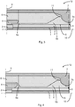
- Fig. 1 is a schematic cross-sectional view of a cable joint 12 provided with an electric field control device.
- the high voltage cable joint 12 comprises a high voltage cable consisting of a cable conductor 1, a cable insulator 2, and a semi-conducting ground layer 8, which are suitably prepared for the cable joint 12.
- a connector 3 is provided as a current connection device.
- the electric field control device comprises an inner deflector 4, a resistive field grading layer 5, an insulating layer 6, i.e. the joint insulation, and a semi-conducting layer 7, i.e. the mantle of the cable joint 12.
- the inner deflector 4 is electrically connected to the cable conductor 1 of the high-voltage cable via the connector 3 during installation of the cable joint 12. To this end, the connector 3 is electrically conductive.
- the inner deflector 4 is electrically semi-conducting.
- the semi-conducting layer 7, e.g. the mantle of the cable joint 12 and the semi-conducting ground layer 8 may instead be of an electrically conducting material.
- the resistive field grading layer 5 has nonlinear current-voltage characteristics and is adapted for field controlling purposes. During the fabrication of the cable joint 12, the resistive field grading layer 5 is arranged along the cable insulator 2 of the high-voltage cable and is at one end (to the right in Fig. 1 ) electrically connected to the semi-conducting ground layer 8 of the high-voltage cable. At one position (to the left in Fig. 1 ) the resistive field grading layer 5 is electrically connected to the inner deflector 4 and will hereby be electrically connected to the cable conductor 1 of the high-voltage cable.
- the insulating layer 6 is arranged on the resistive field grading layer 5 and extends at least from the one position and towards the one end of the resistive field grading layer 5 while ending, e.g. by tapered field control geometry, without reaching the one end of the resistive field grading layer 5.
- the semi-conducting layer 7 is arranged on the insulating layer 6 and extends at least from the one position and towards the one end of the resistive field grading layer 5 and past the end of the insulating layer 6.
- an outer triple point 11 can be defined at the intersection of the resistive field grading layer 5, the insulating layer 6, and the semi-conducting layer 7.
- the semi-conducting ground layer 8 of the high-voltage cable may be electrically connected to the semi-conducting layer 7, e.g. at the right hand of Fig. 1 .
- the resistive field grading layer 5 has first 5a, second 5b, and third 5c adjacent sections as seen from the one position towards the one end of the resistive field grading layer 5 (from left to right in Fig. 1 ), wherein the third section 5c is extending from the outer triple point 11 to the one end of the resistive field grading layer 5.
- a portion of the first section 5a of the resistive field grading layer 5 is in contact with, and extends below, the inner deflector 4 as can be seen in Fig. 1 .
- the portion of the first section 5a, which extends below the inner deflector 4, is in this embodiment, however, not extending so long that it will come into contact with the connector 3.
- FIG. 1 another portion of the first section 5a of the resistive field grading layer 5 is in contact with, and extends above, the inner deflector 4.
- the geometry of the resistive field grading layer 5 effectively prevents a superimposed field due to a DC field and transients of opposite polarity from becoming too high.
- the high voltage cable and the electric field control device may be cylinder symmetrical devices with a rotational symmetry axis 10 in a longitudinal direction.
- Each of the components of the high voltage cable and the electric field control device are rotation symmetric around the longitudinal symmetry axis 10.
- a mirror symmetry plane 9 in a radial direction i.e. the normal vector of the plane is extending in an axial direction
- the components of the high voltage cable and the electric field control device are mirrored to obtain the second high voltage cable of the cable joint 12 (to the left of the radial symmetry plane 9) and the components of the electric field control device, which are connected to that high voltage cable during fabrication of the cable joint 12.
- expressions such as a position, an end, and adjacent may be understood as a longitudinal position, a longitudinal end, and adjacent in the longitudinal direction.
- the inner deflector 4 is electrically connected to the cable conductor of the second high-voltage cable via the connector 3
- the resistive field grading layer 5 is arranged along the cable insulator of the second high-voltage cable and is at a second end electrically connected to the semi-conducting ground layer of the second high-voltage cable.
- the resistive field grading layer 5 is electrically connected to the inner deflector 4 and will hereby be connected to the cable conductor 1 of the high-voltage cable.
- the insulating layer 6 is arranged on the resistive field grading layer 5 and extends at least from the second position and towards the second end of the resistive field grading layer 5 while ending, e.g. by tapered field control geometry, without reaching the second end of the resistive field grading layer 5.
- the semi-conducting layer 7 is arranged on the insulating layer 6 and extends at least from the second position and towards the second end of the resistive field grading layer 5 and past the end of the insulating layer 6, which does not reach the second end of the resistive field grading layer 5.
- a second outer triple point can be defined at the intersection of the resistive field grading layer 5, the insulating layer 6, and the semi-conducting layer 7 at the second high voltage cable.
- the resistive field grading layer 5 has fourth, fifth, and sixth adjacent sections as seen from the second position and towards the second end of the resistive field grading layer 5 (not illustrated), wherein a portion of the fourth section is in contact with, and extends below, the inner deflector 4.
- the second section 5b of the resistive field grading layer 5 has a tapered field control geometry with a gradually increasing thickness in the direction towards the outer triple point 11, whereas the first section 5a of the resistive field grading layer 5 may be a thin uniform layer of a substantially constant thickness.
- the gradually increasing thickness in the direction towards the outer triple point 11 may exist in the entire or at least in a substantial part of the second section 5b of the resistive field grading layer 5.
- the resistive field grading layer 5 is locally diminished in the first section 5a and in the portion of the second section 5b closest to the first section 5a.
- the resistive losses of the resistive field grading layer 5 are lowered, thereby limiting the heat production.
- the third section 5c of the resistive field grading layer 5 may have, at least in a substantial portion thereof, a gradually decreasing thickness in the direction towards the one end of the resistive field grading layer 5.
- the portion of the third section 5c in which the thickness is gradually decreasing in the direction towards the one end of the resistive field grading layer 5, may extend along a major part of the third section 5c, preferably from the outer triple point 11 to a position where the end of the semi-conducting ground layer 8 of the high-voltage cable is located.
- the thickness decrease is preferably curved.
- Above the semi-conducting ground layer 8 of the high-voltage cable the thickness of the third section 5c is preferably constant, whereby the constant can as well become zero, i.e. the resistive layers vanishes in direction of the semi-conducting ground layer 8.
- the rate of the thickness decrease may be decreasing in the direction towards the one end. Also the higher derivatives of the thickness as a function of distance in the direction towards the one end may be negative.
- the thickness may increase from right to left approximately according to a polynomial.
- the distance between the outer triple point 11 and the semi-conducting ground layer 8 is increased, thereby influencing the axial electric field in the interfaces between the cable insulation 2 and the resistive field grading layer 5 and between the resistive field grading layer 5 and the joint insulation 6. It needs to extend a certain length in order to sufficiently distribute the electric field in the axial direction.
- first section 5a of the resistive field grading layer 5 may have a maximum thickness, which is smaller than a minimum thickness of the second section 5b of the resistive field grading layer 5, and the resistive field grading layer 5 may be thickest at the outer triple point 11.
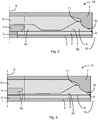
- Fig. 2 is a schematic cross-sectional view of a cable joint 12 provided with an electric field control device, which differs from the electric field control device of Fig. 1 in that the radially extending end side and the upper side of the inner deflector is not covered by the resistive field grading layer 5. Instead, the insulating layer 6 is in contact with, and extends at the radially extending end side and on top of, the inner deflector 4.
- the field grading material of the resistive field grading layer 5 introduces space charge fields. By means of omitting the resistive field grading layer 5 on top of the inner deflector, the space charge field at a critical location such as at the inner deflector 4 is decreased.
- Another alternative could be to provide an electric field control device, which differs from the electric field control device of Fig. 1 in that the radially extending end side and the upper side of the inner deflector is only partly covered by the resistive field grading layer 5, i.e. the resistive field grading layer 5 fade out on top of the inner deflector 4.
- Fig. 3 is a schematic cross-sectional view of a cable joint 12 provided with an electric field control device, which differs from the electric field control device of Fig. 2 in that the portion of the first section 5a of the resistive field grading layer 5, which extends below the inner deflector 4, is extending further to be in contact with, and arranged partly on top of, the connector 3.
- Fig. 4 is a schematic cross-sectional view of a cable joint 12 provided with an electric field control device, which differs from the electric field control device of Fig. 1 in that a portion of the first section 5a of the resistive field grading layer 5 has a gradually increasing thickness in the direction towards the second section 5b, wherein this portion is located at an end of the inner deflector 4.
- a portion of the first section 5a of the resistive field grading layer 5 has a gradually increasing thickness in the direction towards the second section 5b, wherein this portion is located at an end of the inner deflector 4.
- Fig. 5 is a schematic cross-sectional view of a cable joint 12 provided with an electric field control device, which differs from the electric field control device of Fig. 1 in that a portion of the first section 5a of the resistive field grading layer 5 has a gradually increasing thickness in the direction towards the second section 5b, wherein this portion is located at a distance from the radially extending end side of the inner deflector 4 in the direction towards the second section 5b.
- the electric field control device of Fig. 5 is easier and simpler, and thus cheaper, to manufacture as compared to the other illustrated electric field control devices.
- Fig. 6 is a schematic cross-sectional view of a cable joint 12 provided with an electric field control device, which differs from the electric field control device of Fig. 1 in that both a portion of the first section 5a of the resistive field grading layer 5 and a portion of the insulating layer 6 extend below the inner deflector 4. The portion of the first section 5a of the resistive field grading layer 5 does not extend to the inner deflector is only in contact with the connector 3.
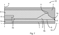
- Fig. 7 is a schematic cross-sectional view of a cable joint 12 provided with an electric field control device, which differs from the electric field control device of Fig. 6 in the portion of the first section 5a of the resistive field grading layer 5 extends to the inner deflector 4, and is thus in contact with the connector 3 and the inner deflector 4.
- the resistive layer 5 may instead extend between the connector 3 and the inner deflector 4 all the way to the mirror symmetry plane 9.
- the high voltage cable joints 12 may carry an alternating voltage or a direct voltage.
- the electric field control devices can be used at various high voltage components such as cable joints, cable terminations, and cable connections, but also as bushings in switchgears and vacuum breakers.
- high voltage components such as cable joints, cable terminations, and cable connections, but also as bushings in switchgears and vacuum breakers.
- no mirror symmetry as illustrated in the drawings is necessary. Axially, the entire device is illustrated in the drawings.
- the electric field control devices disclosed above may be provided for controlling an electric field at a high voltage component, which is rated 300 kV or higher, or optionally 500 kV or higher, and which optionally is a DC high voltage component.
Landscapes
- Emergency Protection Circuit Devices (AREA)
- Connector Housings Or Holding Contact Members (AREA)
- Cable Accessories (AREA)
- Insulation, Fastening Of Motor, Generator Windings (AREA)
- Electron Sources, Ion Sources (AREA)
- Gas-Insulated Switchgears (AREA)
Description
- The present invention generally relates to electric field control.
- There is known a device for controlling an electric field at a high voltage component comprising an inner deflector to be electrically connected to a live high voltage part of the high voltage component; a resistive layer adapted for field controlling purposes, to be arranged along the high voltage component, and which at one position is electrically connected to the inner deflector and at one end is adapted to be electrically connected to a grounded part of the high voltage component; an insulating layer arranged on the resistive layer and extending at least from the one position towards the one end of the resistive layer while ending without reaching the one end of the resistive layer; and a semi-conducting layer arranged on the insulating layer and extending at least from the one position towards the one end of the resistive layer and past the end of the insulating layer, thereby defining an outer triple point at the intersection of the resistive layer, the insulating layer, and the semi-conducting layer.
- A device of this type is known through for instance
WO 00/74191 A1 -
EP1870975 A discloses also a device of this type for controlling an electric field at a high voltage component, the device comprising a resistive layer for field control, an insulating layer arranged on the resistive layer and a semi-conducting or conducting layer arranged on the insulating layer. The three layers meet at a triple point, where the insulating layer ends. The interface between the resistive layer and the insulating layer makes in the triple point an angle to the semi-conducting or conducting layer of 60°-120°.WO 2008/076058 describes a field grading material and a device for grading an electric field at an interruption of the insulation layer arranged around a conductor in a cable. -
US 2003/188885 describes a cylindrical pre-molded rubber insulation tube. A rubber electrode layer is provided and used as a screening electrode to control the concentration of electric stress in insulator. - The rated voltage of HVDC (High Voltage Direct Current) equipment significantly increases and therefore, cable joints and terminations with corresponding voltage levels are required. By the term high voltage is referred to electric voltages of 36 kV and above, or often much higher such as hundreds of kV, such as e.g. above 300 kV and even above 500 kV.
- The main challenge for DC equipment is the combined stress requirements of almost double nominal DC voltages and of DC voltages with superimposed transient voltages, like e.g. switching surges and lightning impulses. For the constant applied DC voltages the conductivity of the material is the dominating parameters. For transients additionally the permittivity needs to be taken into account. A worst case can be seen in the super position of a DC field and a fast transient of opposite polarity. Here extraordinary stress is achieved by superposition of space charge resistive and capacitive field distributions. This may lead to totally different stress distributions for transients and DC applied voltages, separately.
- However, when using the known electric field control devices for voltages, in particular DC voltages, above a determined limit, which is depending on the material used for the different layers, the device will be damaged, thereby limiting the use of such a device with respect to the level of the high voltage.
- It is therefore a purpose to provide an electric field control device, which may be used for higher voltages, in particular DC voltages, than such electric field control devices already known without being damaged.
- The invention, as defined in
claim 1, refers to a device for controlling an electric field at a high voltage component comprising an inner deflector electrically connected to a live high voltage part of the high voltage component; a resistive layer having a nonlinear current-voltage characteristic adapted for electrical field controlling purposes, and arranged along the high voltage component, and which at one position is electrically connected to the inner deflector and at one end is electrically connected to a grounded part of the high voltage component; an insulating layer arranged on the resistive layer and extending at least from the one position towards the one end of the resistive layer while ending, by a tapered field control geometry, without reaching the one end of the resistive layer; and a semi-conducting or conducting layer arranged on the insulating layer and extending at least from the one position towards the one end of the resistive layer and past the end of the insulating layer, thereby defining an outer triple point at the intersection of the resistive layer, the insulating layer, and the semi-conducting or conducting layer. The resistive layer, which exhibits nonlinear current-voltage characteristics, has first, second, and third adjacent sections as seen from the one position towards the one end, wherein a portion of the first section extends below the inner deflector and is in contact with, and extend above, the inner deflector, and is located at an end of the inner deflector. The second section has, in a part thereof, a field control geometry with a gradually increasing thickness in the direction towards the outer triple point. The third section is extending from the outer triple point to an end of the resistive field grading layer. - The electric field control device may comprise a connector, via which the inner deflector is electrically connected to the live high voltage part of the high voltage component, wherein the portion of the first section, which extends below the inner deflector, may be in contact with the connector only, with the inner deflector only, or with both the connector and the inner deflector. The portion of the first section, which extends below the inner deflector, may extend under the inner deflector, a considerable distance, such as e.g. at least under 10, 20, 30, or 40 % of the extension of the inner deflector.
- The portion of the third section, in which the thickness is gradually decreasing in the direction towards the one end, may extend along a major part of the third section.
- Further, the rate of the thickness decrease may decrease in the direction towards the one end.
- The above electric field control devices may be provided for controlling an electric field at a high voltage component, which is rated 300 kV or higher, or optionally 500 kV or higher, and which optionally is a DC high voltage component.
- The main tasks of the electric field control devices are for DC to provide interface grading and to avoid thermal runaway, for AC to keep the electric field below the bulk break down strength and the interface break down strength, and for transients of opposite polarity to keep the superimposed electric field below the bulk break down strength.
- The electric field control devices disclosed in this document lower electric fields in critical locations, increase the break down strength in critical locations, and lower the dissipated power in critical locations. The non-cylindrical shape of the resistive layer differs from the conventional cylindrical form, known in the prior art mentioned in the background section. This new shape gives reduced resistive losses of the resistive field grading layer and thereby limits the heat production that occurs. The resistive field grading layer can thereby be used for higher (DC) voltages without being damaged. Further, the resistive field grading layer is more cost-efficient than known such layers.
- Further characteristics and advantages will be evident from the following detailed description of embodiments given hereinafter and the accompanying
Figs. 1 ,4 and5 , which are given by way of illustration only, and are thus not limitative. -
-
Figs. 1 ,4 and5 are each a schematic cross-sectional view of a cable joint provided with a device for controlling an electric field according to a respective embodiment. -
Figs. 2 ,3 ,6 and7 show examples not describing part of the present invention and are given only as comparative embodiments. - Identical reference numerals are used throughout the Figures to denote identical or similar components, portions, details and the like of the various embodiments.
- The embodiments shown in
figures 2 ,3 ,6 and7 and described in the following detailed description do not form part of or describe the claimed invention and are given only as comparative embodiments and as examples useful for the understanding of the invention. -
Fig. 1 is a schematic cross-sectional view of acable joint 12 provided with an electric field control device. The highvoltage cable joint 12 comprises a high voltage cable consisting of acable conductor 1, acable insulator 2, and asemi-conducting ground layer 8, which are suitably prepared for thecable joint 12. Aconnector 3 is provided as a current connection device. - The electric field control device comprises an
inner deflector 4, a resistivefield grading layer 5, aninsulating layer 6, i.e. the joint insulation, and asemi-conducting layer 7, i.e. the mantle of thecable joint 12. - The
inner deflector 4 is electrically connected to thecable conductor 1 of the high-voltage cable via theconnector 3 during installation of thecable joint 12. To this end, theconnector 3 is electrically conductive. Theinner deflector 4 is electrically semi-conducting. Thesemi-conducting layer 7, e.g. the mantle of thecable joint 12 and thesemi-conducting ground layer 8 may instead be of an electrically conducting material. - The resistive
field grading layer 5 has nonlinear current-voltage characteristics and is adapted for field controlling purposes. During the fabrication of thecable joint 12, the resistivefield grading layer 5 is arranged along thecable insulator 2 of the high-voltage cable and is at one end (to the right inFig. 1 ) electrically connected to thesemi-conducting ground layer 8 of the high-voltage cable. At one position (to the left inFig. 1 ) the resistivefield grading layer 5 is electrically connected to theinner deflector 4 and will hereby be electrically connected to thecable conductor 1 of the high-voltage cable. - The
insulating layer 6 is arranged on the resistivefield grading layer 5 and extends at least from the one position and towards the one end of the resistivefield grading layer 5 while ending, e.g. by tapered field control geometry, without reaching the one end of the resistivefield grading layer 5. Thesemi-conducting layer 7 is arranged on theinsulating layer 6 and extends at least from the one position and towards the one end of the resistivefield grading layer 5 and past the end of theinsulating layer 6. Hereby, an outertriple point 11 can be defined at the intersection of the resistivefield grading layer 5, theinsulating layer 6, and thesemi-conducting layer 7. - The
semi-conducting ground layer 8 of the high-voltage cable may be electrically connected to thesemi-conducting layer 7, e.g. at the right hand ofFig. 1 . - The resistive
field grading layer 5 has first 5a, second 5b, and third 5c adjacent sections as seen from the one position towards the one end of the resistive field grading layer 5 (from left to right inFig. 1 ), wherein thethird section 5c is extending from the outertriple point 11 to the one end of the resistivefield grading layer 5. - A portion of the
first section 5a of the resistivefield grading layer 5 is in contact with, and extends below, theinner deflector 4 as can be seen inFig. 1 . The portion of thefirst section 5a, which extends below theinner deflector 4, is in this embodiment, however, not extending so long that it will come into contact with theconnector 3. - As can be seen in
Fig. 1 another portion of thefirst section 5a of the resistivefield grading layer 5 is in contact with, and extends above, theinner deflector 4. - The geometry of the resistive
field grading layer 5 effectively prevents a superimposed field due to a DC field and transients of opposite polarity from becoming too high. - It shall be appreciated that the high voltage cable and the electric field control device may be cylinder symmetrical devices with a
rotational symmetry axis 10 in a longitudinal direction. Each of the components of the high voltage cable and the electric field control device are rotation symmetric around thelongitudinal symmetry axis 10. - Therefore, expressions such as arranged on, above and on top of may be understood as arranged outside or outside of, whereas arranged below and under may be understood as arranged inside or inside of.
- Further, there is a
mirror symmetry plane 9 in a radial direction (i.e. the normal vector of the plane is extending in an axial direction), in which the components of the high voltage cable and the electric field control device are mirrored to obtain the second high voltage cable of the cable joint 12 (to the left of the radial symmetry plane 9) and the components of the electric field control device, which are connected to that high voltage cable during fabrication of thecable joint 12. - Therefore, expressions such as a position, an end, and adjacent may be understood as a longitudinal position, a longitudinal end, and adjacent in the longitudinal direction.
- Thus, during the fabrication of the cable joint 12, the
inner deflector 4 is electrically connected to the cable conductor of the second high-voltage cable via theconnector 3, the resistivefield grading layer 5 is arranged along the cable insulator of the second high-voltage cable and is at a second end electrically connected to the semi-conducting ground layer of the second high-voltage cable. - At a second position (to the left of the
radial symmetry plane 9 inFig. 1 ) the resistivefield grading layer 5 is electrically connected to theinner deflector 4 and will hereby be connected to thecable conductor 1 of the high-voltage cable. - The insulating
layer 6 is arranged on the resistivefield grading layer 5 and extends at least from the second position and towards the second end of the resistivefield grading layer 5 while ending, e.g. by tapered field control geometry, without reaching the second end of the resistivefield grading layer 5. Thesemi-conducting layer 7 is arranged on the insulatinglayer 6 and extends at least from the second position and towards the second end of the resistivefield grading layer 5 and past the end of the insulatinglayer 6, which does not reach the second end of the resistivefield grading layer 5. Hereby, a second outer triple point can be defined at the intersection of the resistivefield grading layer 5, the insulatinglayer 6, and thesemi-conducting layer 7 at the second high voltage cable. - The resistive
field grading layer 5 has fourth, fifth, and sixth adjacent sections as seen from the second position and towards the second end of the resistive field grading layer 5 (not illustrated), wherein a portion of the fourth section is in contact with, and extends below, theinner deflector 4. - It shall be appreciated, that in the following each of the cable joints 12 will be described only with references to the parts illustrated in
Figs. 1-7 , wherein onlyfigures 1 ,4 and5 form part of the present invention. A person skilled in the art realizes that the devices can be rotation symmetric around thelongitudinal symmetry axis 10 and mirrored in theradial symmetry plane 9. - The
second section 5b of the resistivefield grading layer 5 has a tapered field control geometry with a gradually increasing thickness in the direction towards the outertriple point 11, whereas thefirst section 5a of the resistivefield grading layer 5 may be a thin uniform layer of a substantially constant thickness. The gradually increasing thickness in the direction towards the outertriple point 11 may exist in the entire or at least in a substantial part of thesecond section 5b of the resistivefield grading layer 5. - As compared to prior art devices, the resistive
field grading layer 5 is locally diminished in thefirst section 5a and in the portion of thesecond section 5b closest to thefirst section 5a. Hereby, the resistive losses of the resistivefield grading layer 5 are lowered, thereby limiting the heat production. - Further, by reducing the thickness of the resistive
field grading layer 5 to obtain a thin layer possibly covering theinner deflector 4 an additional capacitive/refractive field grading effect, due to the higher permittivity of the material of the resistivefield grading layer 5 as compared to the surrounding material, is obtained. The use of the higher epsilon for fast transients is obtained by the combination of the nonlinear resistive grading with the refractive/capacitive field grading. - Further, the
third section 5c of the resistivefield grading layer 5 may have, at least in a substantial portion thereof, a gradually decreasing thickness in the direction towards the one end of the resistivefield grading layer 5. - The portion of the
third section 5c, in which the thickness is gradually decreasing in the direction towards the one end of the resistivefield grading layer 5, may extend along a major part of thethird section 5c, preferably from the outertriple point 11 to a position where the end of thesemi-conducting ground layer 8 of the high-voltage cable is located. The thickness decrease is preferably curved. Above thesemi-conducting ground layer 8 of the high-voltage cable the thickness of thethird section 5c is preferably constant, whereby the constant can as well become zero, i.e. the resistive layers vanishes in direction of thesemi-conducting ground layer 8. - The rate of the thickness decrease may be decreasing in the direction towards the one end. Also the higher derivatives of the thickness as a function of distance in the direction towards the one end may be negative.
- The thickness t may gradually decrease in the direction towards the one end of the resistive
field grading layer 5 approximately according to
t = C1 e-c 2 x, where C1 and C2 are constants and x is the longitudinal distance from the outertriple point 11. - Alternatively, the thickness may decrease approximately according to a functional form, which may be approximated, e.g. by a geometric series form:

- Still alternatively, the thickness may decrease approximately according to a functional form, which may be approximated by:


triple point 11. - Yet alternatively, the thickness may increase from right to left approximately according to a polynomial.
- By the wedge or stress cone like surface shape of the resistive
field grading layer 5 in thethird section 5c, the distance between the outertriple point 11 and thesemi-conducting ground layer 8 is increased, thereby influencing the axial electric field in the interfaces between thecable insulation 2 and the resistivefield grading layer 5 and between the resistivefield grading layer 5 and thejoint insulation 6. It needs to extend a certain length in order to sufficiently distribute the electric field in the axial direction. - Further, the
first section 5a of the resistivefield grading layer 5 may have a maximum thickness, which is smaller than a minimum thickness of thesecond section 5b of the resistivefield grading layer 5, and the resistivefield grading layer 5 may be thickest at the outertriple point 11. -
Fig. 2 , not describing the present invention but given only as comparative examples useful for understanding the present invention, is a schematic cross-sectional view of a cable joint 12 provided with an electric field control device, which differs from the electric field control device ofFig. 1 in that the radially extending end side and the upper side of the inner deflector is not covered by the resistivefield grading layer 5. Instead, the insulatinglayer 6 is in contact with, and extends at the radially extending end side and on top of, theinner deflector 4. - The field grading material of the resistive
field grading layer 5 introduces space charge fields. By means of omitting the resistivefield grading layer 5 on top of the inner deflector, the space charge field at a critical location such as at theinner deflector 4 is decreased. - Another alternative could be to provide an electric field control device, which differs from the electric field control device of
Fig. 1 in that the radially extending end side and the upper side of the inner deflector is only partly covered by the resistivefield grading layer 5, i.e. the resistivefield grading layer 5 fade out on top of theinner deflector 4. -
Fig. 3 , not describing the present invention but given only as comparative examples useful for understanding the present invention, is a schematic cross-sectional view of a cable joint 12 provided with an electric field control device, which differs from the electric field control device ofFig. 2 in that the portion of thefirst section 5a of the resistivefield grading layer 5, which extends below theinner deflector 4, is extending further to be in contact with, and arranged partly on top of, theconnector 3. - By such provisions a low risk of electric break down is obtained.
-
Fig. 4 , illustrating embodiments of the present invention, is a schematic cross-sectional view of a cable joint 12 provided with an electric field control device, which differs from the electric field control device ofFig. 1 in that a portion of thefirst section 5a of the resistivefield grading layer 5 has a gradually increasing thickness in the direction towards thesecond section 5b, wherein this portion is located at an end of theinner deflector 4. Hereby, any sharp edge of the resistivefield grading layer 5 is avoided, and instead a smooth upper surface of the resistivefield grading layer 5 is obtained as can be seen inFig. 4 . - By means of the
Fig. 4 shape of the resistive field grading layer the electric field due to a DC field and occurring transients can be kept below the bulk break down strength. -
Fig. 5 is a schematic cross-sectional view of a cable joint 12 provided with an electric field control device, which differs from the electric field control device ofFig. 1 in that a portion of thefirst section 5a of the resistivefield grading layer 5 has a gradually increasing thickness in the direction towards thesecond section 5b, wherein this portion is located at a distance from the radially extending end side of theinner deflector 4 in the direction towards thesecond section 5b. - The electric field control device of
Fig. 5 is easier and simpler, and thus cheaper, to manufacture as compared to the other illustrated electric field control devices. -
Fig. 6 , not describing the present invention but given only as comparative examples useful for understanding the present invention, is a schematic cross-sectional view of a cable joint 12 provided with an electric field control device, which differs from the electric field control device ofFig. 1 in that both a portion of thefirst section 5a of the resistivefield grading layer 5 and a portion of the insulatinglayer 6 extend below theinner deflector 4. The portion of thefirst section 5a of the resistivefield grading layer 5 does not extend to the inner deflector is only in contact with theconnector 3. -
Fig. 7 , not describing the present invention but given only as comparative examples useful for understanding the present invention, is a schematic cross-sectional view of a cable joint 12 provided with an electric field control device, which differs from the electric field control device ofFig. 6 in the portion of thefirst section 5a of the resistivefield grading layer 5 extends to theinner deflector 4, and is thus in contact with theconnector 3 and theinner deflector 4. - The
resistive layer 5 may instead extend between theconnector 3 and theinner deflector 4 all the way to themirror symmetry plane 9. - The high voltage cable joints 12 may carry an alternating voltage or a direct voltage.
- Generally, the electric field control devices can be used at various high voltage components such as cable joints, cable terminations, and cable connections, but also as bushings in switchgears and vacuum breakers. Here, no mirror symmetry as illustrated in the drawings is necessary. Axially, the entire device is illustrated in the drawings.
- Advantageously, the electric field control devices disclosed above may be provided for controlling an electric field at a high voltage component, which is rated 300 kV or higher, or optionally 500 kV or higher, and which optionally is a DC high voltage component.
Claims (13)
- A device for controlling an electric field at a high voltage component comprising:- an inner deflector (4) electrically connected to a live high voltage part (1) of the high voltage component;- a resistive layer (5) having a nonlinear current-voltage characteristics adapted for electric field controlling purposes, and arranged along said high voltage component, and which at one position is connected to the inner deflector (4) and at one end electrically connected to a grounded part (8) of the high voltage component;- an insulating layer (6) arranged on said resistive layer (5) and extending at least from said one position towards said one end of the resistive layer (5) while ending without reaching said one end of the resistive layer (5); and- a semi-conducting or conducting layer (7) arranged on the insulating layer (6) and extending at least from said one position towards said one end of the resistive layer (5) and past the end of the insulating layer (6), thereby defining an outer triple point (11) at the intersection of the resistive layer (5), the insulating layer (6), and the semi- conducting or conducting layer (7)characterized in that- the resistive layer (5) has first, second, and third adjacent sections (5a, 5b, 5c) as seen from said one position towards said one end, wherein- a portion of the first section (5a) extends below said inner deflector (4) and is in contact with, and extend above, the inner deflector (4), and is located at an end of the inner deflector (4),- the second section (5b) has, in a part thereof, a gradually increasing thickness in the direction towards the outer triple point (11), and- the third section (5c) is extending from the outer triple point (11) to an end of the resistive field grading layer (5).
- The device of claim 1 comprising a connector (3), via which said inner deflector (4) is electrically connected to said live high voltage part (1) of the high voltage component.
- The device of claim 2 wherein said portion of the first section (5a), which extends below said inner deflector (4), is in contact with said inner deflector (4) only, or with both the connector (3) and the inner deflector (4).
- The device of any of claims 1-3 wherein a portion of the first section (5a) has a gradually increasing thickness in the direction towards the second section (5b).
- The device of any of claims 1- 4 wherein the third section (5c) has, at least in a substantial portion thereof, a gradually decreasing thickness in the direction towards said one end.
- The device of claim 5 wherein the portion of the third section (5c), in which the thickness is gradually decreasing in the direction towards said one end, extends from the outer triple point to the end of a ground part (8) of the high voltage component.
- The device of claim 5 or 6 wherein the rate of the thickness decrease is decreasing in the direction towards said one end.
- The device of any of claims 1-7 wherein the resistive layer (5) is thickest at the outer triple point (11).
- The device of any of claims 1-8 wherein- said device is arranged for controlling an electric field at a further high voltage component;- said inner deflector (4) is electrically connected to a live high voltage part of the further high voltage component;- said resistive layer (5) is arranged along said further high voltage component, and which at one further position is electrically connected to said live high voltage part of the further high voltage component and at one other end is adapted to be electrically connected to a grounded part of the further high voltage component;- said insulating layer (6) is extending at least from said one further position towards said one other end of the resistive layer (5) while ending without reaching said one other end of the resistive layer (5);- said semi-conducting or conducting layer (7) arranged on the insulating layer (6) and extending at least from said one further position towards said one other end of the resistive layer (5) and past the end of the insulating layer (6), thereby defining a further outer triple point at an intersection of the resistive layer (5), the insulating layer (6), and the semi-conducting or conducting layer (7);- the resistive layer (5) has fourth, fifth, and sixth adjacent sections as seen from said one further position towards said one other end, wherein- a portion of the fourth section extends below said inner deflector (4).
- The device of claim 9, wherein- the high voltage component and the further high voltage component are each a high voltage cable; and- said device is provided for jointing the high voltage cables in a cable joint.
- The device of any of claims 1-10 wherein- the high voltage component is a high voltage cable, switchgear, or a vacuum breaker; and- said device is provided for terminating said high voltage cable in a cable termination or for being used as a bushing.
- The device of any of claims 1-11 wherein said device is provided for controlling an electric field at a high voltage component, which is rated 300 kV or higher, or optionally 500 kV or higher, and which optionally is a DC high voltage component.
- The device of any of claims 1 - 12, wherein the resistive layer (5) is locally diminished in the first section (5a) and in the portion of the second section (5b) closest to the first section (5a).
Applications Claiming Priority (2)
| Application Number | Priority Date | Filing Date | Title |
|---|---|---|---|
| US201161504342P | 2011-07-05 | 2011-07-05 | |
| PCT/EP2012/063041 WO2013004748A2 (en) | 2011-07-05 | 2012-07-04 | A device for electric field control |
Publications (2)
| Publication Number | Publication Date |
|---|---|
| EP2730002A2 EP2730002A2 (en) | 2014-05-14 |
| EP2730002B1 true EP2730002B1 (en) | 2021-07-28 |
Family
ID=46545753
Family Applications (1)
| Application Number | Title | Priority Date | Filing Date |
|---|---|---|---|
| EP12737511.1A Active EP2730002B1 (en) | 2011-07-05 | 2012-07-04 | A device for electric field control |
Country Status (8)
| Country | Link |
|---|---|
| US (1) | US9263875B2 (en) |
| EP (1) | EP2730002B1 (en) |
| JP (1) | JP5805865B2 (en) |
| KR (1) | KR101578628B1 (en) |
| CN (1) | CN103718404B (en) |
| AU (1) | AU2012280287B9 (en) |
| IN (1) | IN2014CN00774A (en) |
| WO (1) | WO2013004748A2 (en) |
Families Citing this family (17)
| Publication number | Priority date | Publication date | Assignee | Title |
|---|---|---|---|---|
| CN103718404B (en) | 2011-07-05 | 2018-04-10 | Abb Hv电缆瑞士有限责任公司 | Equipment for electric field controls |
| US9306340B2 (en) | 2013-12-13 | 2016-04-05 | General Electric Company | System and method for sub-sea cable termination |
| KR102238971B1 (en) | 2014-02-21 | 2021-04-12 | 엘에스전선 주식회사 | Termination connection box for DC cable |
| EP3183788B1 (en) * | 2014-08-22 | 2020-04-08 | NKT HV Cables AB | Electric field control device for high power cable and method for manufacturing thereof |
| CH710800B1 (en) * | 2015-08-27 | 2016-08-31 | Gramespacher Hansjörg | Prefabricated socket body for the connection of two high-voltage polymer cables for DC. |
| US10903639B2 (en) | 2016-09-19 | 2021-01-26 | Prysmian S.P.A. | Joint for high voltage direct current cables |
| AU2017414065B2 (en) * | 2017-05-11 | 2022-04-21 | Prysmian S.P.A. | Cable termination system, termination assembly and method for installing such a termination assembly |
| US11476614B2 (en) | 2017-05-11 | 2022-10-18 | Prysmian S.P.A. | Cable termination system, termination assembly and method for installing such a termination assembly |
| NO20170997A1 (en) | 2017-06-16 | 2018-11-26 | Benestad Solutions As | High voltage wet-mate connection assembly |
| WO2019012885A1 (en) * | 2017-07-13 | 2019-01-17 | 住友電気工業株式会社 | Non-ohmic composition and method for manufacturing same, cable interconnect unit and cable end-connect unit |
| US11939461B2 (en) | 2019-01-18 | 2024-03-26 | Sumitomo Electric Industries, Ltd. | Non-ohmic composition, cable connection unit, and method for producing cable connection unit |
| KR102676932B1 (en) * | 2019-01-18 | 2024-06-19 | 스미토모 덴키 고교 가부시키가이샤 | Non-ohmic composition, cable connection unit, and method for producing cable connection unit |
| JP7572669B2 (en) * | 2019-12-04 | 2024-10-24 | 株式会社朝日ラバー | Joint of object to be joined and functional substrate |
| KR20230175124A (en) * | 2022-06-21 | 2023-12-29 | 엘에스전선 주식회사 | DC Power Cable System |
| KR20230175125A (en) * | 2022-06-21 | 2023-12-29 | 엘에스전선 주식회사 | DC Power Cable System |
| EP4586423A1 (en) * | 2024-01-15 | 2025-07-16 | NKT HV Cables AB | Hvdc cable accessories based on thermoplastic elastomers |
| FR3158839A1 (en) * | 2024-01-29 | 2025-08-01 | Safran Electrical & Power | Electrical connection device |
Family Cites Families (9)
| Publication number | Priority date | Publication date | Assignee | Title |
|---|---|---|---|---|
| EP0491091A1 (en) * | 1990-12-19 | 1992-06-24 | Siemens Aktiengesellschaft | Plastic high-voltage cable with slip-on control element |
| JPH0731044A (en) * | 1993-07-09 | 1995-01-31 | Fujikura Ltd | Insulating resin molded product |
| SE514209C2 (en) | 1999-05-28 | 2001-01-22 | Abb Ab | Control of electric field at direct voltage |
| CN1324778C (en) * | 2001-11-27 | 2007-07-04 | 株式会社藤仓 | Structure and part for electric cable connection and making method thereof |
| CA2503141C (en) * | 2002-10-30 | 2010-12-21 | Pirelli & C. S.P.A. | Process for manufacturing the elastomeric sleeve of a joint for electrical cables and manufacturing apparatus thereof |
| JP4158904B2 (en) * | 2003-04-18 | 2008-10-01 | 古河電気工業株式会社 | Normal temperature shrinkable rubber unit |
| EP1870975B1 (en) | 2006-06-21 | 2010-08-04 | ABB Technology Ltd | A device for electric field control |
| SE531409C2 (en) * | 2006-12-20 | 2009-03-24 | Abb Research Ltd | Field-controlling material |
| CN103718404B (en) | 2011-07-05 | 2018-04-10 | Abb Hv电缆瑞士有限责任公司 | Equipment for electric field controls |
-
2012
- 2012-07-04 CN CN201280033327.8A patent/CN103718404B/en not_active Expired - Fee Related
- 2012-07-04 JP JP2014517791A patent/JP5805865B2/en active Active
- 2012-07-04 WO PCT/EP2012/063041 patent/WO2013004748A2/en not_active Ceased
- 2012-07-04 AU AU2012280287A patent/AU2012280287B9/en active Active
- 2012-07-04 IN IN774CHN2014 patent/IN2014CN00774A/en unknown
- 2012-07-04 EP EP12737511.1A patent/EP2730002B1/en active Active
- 2012-07-04 KR KR1020147002740A patent/KR101578628B1/en active Active
-
2014
- 2014-01-06 US US14/148,347 patent/US9263875B2/en active Active
Non-Patent Citations (1)
| Title |
|---|
| None * |
Also Published As
| Publication number | Publication date |
|---|---|
| KR20140030330A (en) | 2014-03-11 |
| CN103718404B (en) | 2018-04-10 |
| CN103718404A (en) | 2014-04-09 |
| US20140116746A1 (en) | 2014-05-01 |
| AU2012280287B2 (en) | 2015-07-16 |
| US9263875B2 (en) | 2016-02-16 |
| IN2014CN00774A (en) | 2015-04-03 |
| WO2013004748A2 (en) | 2013-01-10 |
| WO2013004748A3 (en) | 2013-11-07 |
| EP2730002A2 (en) | 2014-05-14 |
| JP2014518500A (en) | 2014-07-28 |
| KR101578628B1 (en) | 2015-12-17 |
| AU2012280287A1 (en) | 2014-01-16 |
| JP5805865B2 (en) | 2015-11-10 |
| AU2012280287B9 (en) | 2015-07-23 |
Similar Documents
| Publication | Publication Date | Title |
|---|---|---|
| US9263875B2 (en) | Device for electric field control | |
| US20180219369A1 (en) | Cable fitting for connecting a high-voltage cable to a high-voltage component | |
| US20130153267A1 (en) | Device for electric field control | |
| EP2572422A2 (en) | A high voltage direct current cable termination apparatus | |
| EP2057643B1 (en) | High voltage dc bushing and device comprising such high voltage bushing | |
| EP1188209A1 (en) | Control of electric field at direct voltage | |
| EP3516749B1 (en) | Joint for high voltage direct current cables | |
| EP2572424A2 (en) | A high voltage direct current cable termination apparatus | |
| JP2006296190A (en) | Synthetic material end unit of dc electric cable | |
| EP3622600B1 (en) | Cable termination system, termination assembly and method for installing such a termination assembly | |
| AU2014383641B2 (en) | Power cable termination device for gas-insulated switchgear | |
| RU97013U1 (en) | CONNECTING CLUTCH FOR POWER CABLE | |
| EP3933870A1 (en) | High frequency transients suppression for hvdisconnectors with sliding resistor | |
| Hou et al. | Influential factor analysis and computation on electric field of converter transformer barrier | |
| US11476614B2 (en) | Cable termination system, termination assembly and method for installing such a termination assembly | |
| CN206742825U (en) | A kind of electric stress key-course for high voltage direct current cable joint | |
| CN205724824U (en) | Stress control body | |
| KR20190083504A (en) | Electric field control device | |
| JP2015226436A (en) | Gas-insulated switchgear |
Legal Events
| Date | Code | Title | Description |
|---|---|---|---|
| PUAI | Public reference made under article 153(3) epc to a published international application that has entered the european phase |
Free format text: ORIGINAL CODE: 0009012 |
|
| 17P | Request for examination filed |
Effective date: 20140128 |
|
| AK | Designated contracting states |
Kind code of ref document: A2 Designated state(s): AL AT BE BG CH CY CZ DE DK EE ES FI FR GB GR HR HU IE IS IT LI LT LU LV MC MK MT NL NO PL PT RO RS SE SI SK SM TR |
|
| AX | Request for extension of the european patent |
Extension state: BA ME |
|
| R17P | Request for examination filed (corrected) |
Effective date: 20140507 |
|
| RBV | Designated contracting states (corrected) |
Designated state(s): AL AT BE BG CH CY CZ DE DK EE ES FI FR GB GR HR HU IE IS IT LI LT LU LV MC MK MT NL NO PL PT RO RS SE SI SK SM TR |
|
| DAX | Request for extension of the european patent (deleted) | ||
| RAP1 | Party data changed (applicant data changed or rights of an application transferred) |
Owner name: ABB HV CABLES (SWITZERLAND) GMBH |
|
| RAP1 | Party data changed (applicant data changed or rights of an application transferred) |
Owner name: NKT HV CABLES GMBH |
|
| STAA | Information on the status of an ep patent application or granted ep patent |
Free format text: STATUS: EXAMINATION IS IN PROGRESS |
|
| 17Q | First examination report despatched |
Effective date: 20191028 |
|
| RAP1 | Party data changed (applicant data changed or rights of an application transferred) |
Owner name: NKT HV CABLES AB |
|
| GRAP | Despatch of communication of intention to grant a patent |
Free format text: ORIGINAL CODE: EPIDOSNIGR1 |
|
| STAA | Information on the status of an ep patent application or granted ep patent |
Free format text: STATUS: GRANT OF PATENT IS INTENDED |
|
| RIC1 | Information provided on ipc code assigned before grant |
Ipc: H02G 15/068 20060101AFI20210201BHEP Ipc: H02G 15/105 20060101ALI20210201BHEP |
|
| INTG | Intention to grant announced |
Effective date: 20210224 |
|
| GRAS | Grant fee paid |
Free format text: ORIGINAL CODE: EPIDOSNIGR3 |
|
| GRAA | (expected) grant |
Free format text: ORIGINAL CODE: 0009210 |
|
| STAA | Information on the status of an ep patent application or granted ep patent |
Free format text: STATUS: THE PATENT HAS BEEN GRANTED |
|
| AK | Designated contracting states |
Kind code of ref document: B1 Designated state(s): AL AT BE BG CH CY CZ DE DK EE ES FI FR GB GR HR HU IE IS IT LI LT LU LV MC MK MT NL NO PL PT RO RS SE SI SK SM TR |
|
| REG | Reference to a national code |
Ref country code: GB Ref legal event code: FG4D |
|
| RIN1 | Information on inventor provided before grant (corrected) |
Inventor name: RAPP, HANS Inventor name: MING, LI Inventor name: UNGE, MIKAEL Inventor name: GAEFVERT, UNO Inventor name: SALTZER, MARKUS |
|
| REG | Reference to a national code |
Ref country code: CH Ref legal event code: EP |
|
| REG | Reference to a national code |
Ref country code: AT Ref legal event code: REF Ref document number: 1415570 Country of ref document: AT Kind code of ref document: T Effective date: 20210815 |
|
| REG | Reference to a national code |
Ref country code: IE Ref legal event code: FG4D |
|
| REG | Reference to a national code |
Ref country code: DE Ref legal event code: R096 Ref document number: 602012076220 Country of ref document: DE |
|
| REG | Reference to a national code |
Ref country code: LT Ref legal event code: MG9D |
|
| REG | Reference to a national code |
Ref country code: NL Ref legal event code: FP |
|
| REG | Reference to a national code |
Ref country code: AT Ref legal event code: MK05 Ref document number: 1415570 Country of ref document: AT Kind code of ref document: T Effective date: 20210728 |
|
| PG25 | Lapsed in a contracting state [announced via postgrant information from national office to epo] |
Ref country code: AT Free format text: LAPSE BECAUSE OF FAILURE TO SUBMIT A TRANSLATION OF THE DESCRIPTION OR TO PAY THE FEE WITHIN THE PRESCRIBED TIME-LIMIT Effective date: 20210728 Ref country code: BG Free format text: LAPSE BECAUSE OF FAILURE TO SUBMIT A TRANSLATION OF THE DESCRIPTION OR TO PAY THE FEE WITHIN THE PRESCRIBED TIME-LIMIT Effective date: 20211028 Ref country code: LT Free format text: LAPSE BECAUSE OF FAILURE TO SUBMIT A TRANSLATION OF THE DESCRIPTION OR TO PAY THE FEE WITHIN THE PRESCRIBED TIME-LIMIT Effective date: 20210728 Ref country code: RS Free format text: LAPSE BECAUSE OF FAILURE TO SUBMIT A TRANSLATION OF THE DESCRIPTION OR TO PAY THE FEE WITHIN THE PRESCRIBED TIME-LIMIT Effective date: 20210728 Ref country code: NO Free format text: LAPSE BECAUSE OF FAILURE TO SUBMIT A TRANSLATION OF THE DESCRIPTION OR TO PAY THE FEE WITHIN THE PRESCRIBED TIME-LIMIT Effective date: 20211028 Ref country code: PT Free format text: LAPSE BECAUSE OF FAILURE TO SUBMIT A TRANSLATION OF THE DESCRIPTION OR TO PAY THE FEE WITHIN THE PRESCRIBED TIME-LIMIT Effective date: 20211129 Ref country code: ES Free format text: LAPSE BECAUSE OF FAILURE TO SUBMIT A TRANSLATION OF THE DESCRIPTION OR TO PAY THE FEE WITHIN THE PRESCRIBED TIME-LIMIT Effective date: 20210728 Ref country code: FI Free format text: LAPSE BECAUSE OF FAILURE TO SUBMIT A TRANSLATION OF THE DESCRIPTION OR TO PAY THE FEE WITHIN THE PRESCRIBED TIME-LIMIT Effective date: 20210728 Ref country code: HR Free format text: LAPSE BECAUSE OF FAILURE TO SUBMIT A TRANSLATION OF THE DESCRIPTION OR TO PAY THE FEE WITHIN THE PRESCRIBED TIME-LIMIT Effective date: 20210728 Ref country code: SE Free format text: LAPSE BECAUSE OF FAILURE TO SUBMIT A TRANSLATION OF THE DESCRIPTION OR TO PAY THE FEE WITHIN THE PRESCRIBED TIME-LIMIT Effective date: 20210728 |
|
| PG25 | Lapsed in a contracting state [announced via postgrant information from national office to epo] |
Ref country code: PL Free format text: LAPSE BECAUSE OF FAILURE TO SUBMIT A TRANSLATION OF THE DESCRIPTION OR TO PAY THE FEE WITHIN THE PRESCRIBED TIME-LIMIT Effective date: 20210728 Ref country code: LV Free format text: LAPSE BECAUSE OF FAILURE TO SUBMIT A TRANSLATION OF THE DESCRIPTION OR TO PAY THE FEE WITHIN THE PRESCRIBED TIME-LIMIT Effective date: 20210728 Ref country code: GR Free format text: LAPSE BECAUSE OF FAILURE TO SUBMIT A TRANSLATION OF THE DESCRIPTION OR TO PAY THE FEE WITHIN THE PRESCRIBED TIME-LIMIT Effective date: 20211029 |
|
| PG25 | Lapsed in a contracting state [announced via postgrant information from national office to epo] |
Ref country code: DK Free format text: LAPSE BECAUSE OF FAILURE TO SUBMIT A TRANSLATION OF THE DESCRIPTION OR TO PAY THE FEE WITHIN THE PRESCRIBED TIME-LIMIT Effective date: 20210728 |
|
| REG | Reference to a national code |
Ref country code: DE Ref legal event code: R097 Ref document number: 602012076220 Country of ref document: DE |
|
| PG25 | Lapsed in a contracting state [announced via postgrant information from national office to epo] |
Ref country code: SM Free format text: LAPSE BECAUSE OF FAILURE TO SUBMIT A TRANSLATION OF THE DESCRIPTION OR TO PAY THE FEE WITHIN THE PRESCRIBED TIME-LIMIT Effective date: 20210728 Ref country code: SK Free format text: LAPSE BECAUSE OF FAILURE TO SUBMIT A TRANSLATION OF THE DESCRIPTION OR TO PAY THE FEE WITHIN THE PRESCRIBED TIME-LIMIT Effective date: 20210728 Ref country code: RO Free format text: LAPSE BECAUSE OF FAILURE TO SUBMIT A TRANSLATION OF THE DESCRIPTION OR TO PAY THE FEE WITHIN THE PRESCRIBED TIME-LIMIT Effective date: 20210728 Ref country code: EE Free format text: LAPSE BECAUSE OF FAILURE TO SUBMIT A TRANSLATION OF THE DESCRIPTION OR TO PAY THE FEE WITHIN THE PRESCRIBED TIME-LIMIT Effective date: 20210728 Ref country code: CZ Free format text: LAPSE BECAUSE OF FAILURE TO SUBMIT A TRANSLATION OF THE DESCRIPTION OR TO PAY THE FEE WITHIN THE PRESCRIBED TIME-LIMIT Effective date: 20210728 Ref country code: AL Free format text: LAPSE BECAUSE OF FAILURE TO SUBMIT A TRANSLATION OF THE DESCRIPTION OR TO PAY THE FEE WITHIN THE PRESCRIBED TIME-LIMIT Effective date: 20210728 |
|
| PLBE | No opposition filed within time limit |
Free format text: ORIGINAL CODE: 0009261 |
|
| STAA | Information on the status of an ep patent application or granted ep patent |
Free format text: STATUS: NO OPPOSITION FILED WITHIN TIME LIMIT |
|
| 26N | No opposition filed |
Effective date: 20220429 |
|
| PG25 | Lapsed in a contracting state [announced via postgrant information from national office to epo] |
Ref country code: MC Free format text: LAPSE BECAUSE OF FAILURE TO SUBMIT A TRANSLATION OF THE DESCRIPTION OR TO PAY THE FEE WITHIN THE PRESCRIBED TIME-LIMIT Effective date: 20210728 |
|
| REG | Reference to a national code |
Ref country code: CH Ref legal event code: PL |
|
| REG | Reference to a national code |
Ref country code: BE Ref legal event code: MM Effective date: 20220731 |
|
| PG25 | Lapsed in a contracting state [announced via postgrant information from national office to epo] |
Ref country code: LU Free format text: LAPSE BECAUSE OF NON-PAYMENT OF DUE FEES Effective date: 20220704 Ref country code: LI Free format text: LAPSE BECAUSE OF NON-PAYMENT OF DUE FEES Effective date: 20220731 Ref country code: CH Free format text: LAPSE BECAUSE OF NON-PAYMENT OF DUE FEES Effective date: 20220731 |
|
| PG25 | Lapsed in a contracting state [announced via postgrant information from national office to epo] |
Ref country code: BE Free format text: LAPSE BECAUSE OF NON-PAYMENT OF DUE FEES Effective date: 20220731 |
|
| P01 | Opt-out of the competence of the unified patent court (upc) registered |
Effective date: 20230527 |
|
| PG25 | Lapsed in a contracting state [announced via postgrant information from national office to epo] |
Ref country code: IE Free format text: LAPSE BECAUSE OF NON-PAYMENT OF DUE FEES Effective date: 20220704 |
|
| PG25 | Lapsed in a contracting state [announced via postgrant information from national office to epo] |
Ref country code: HU Free format text: LAPSE BECAUSE OF FAILURE TO SUBMIT A TRANSLATION OF THE DESCRIPTION OR TO PAY THE FEE WITHIN THE PRESCRIBED TIME-LIMIT; INVALID AB INITIO Effective date: 20120704 |
|
| PG25 | Lapsed in a contracting state [announced via postgrant information from national office to epo] |
Ref country code: MK Free format text: LAPSE BECAUSE OF FAILURE TO SUBMIT A TRANSLATION OF THE DESCRIPTION OR TO PAY THE FEE WITHIN THE PRESCRIBED TIME-LIMIT Effective date: 20210728 Ref country code: CY Free format text: LAPSE BECAUSE OF FAILURE TO SUBMIT A TRANSLATION OF THE DESCRIPTION OR TO PAY THE FEE WITHIN THE PRESCRIBED TIME-LIMIT Effective date: 20210728 |
|
| PG25 | Lapsed in a contracting state [announced via postgrant information from national office to epo] |
Ref country code: MT Free format text: LAPSE BECAUSE OF FAILURE TO SUBMIT A TRANSLATION OF THE DESCRIPTION OR TO PAY THE FEE WITHIN THE PRESCRIBED TIME-LIMIT Effective date: 20210728 |
|
| PGFP | Annual fee paid to national office [announced via postgrant information from national office to epo] |
Ref country code: NL Payment date: 20250715 Year of fee payment: 14 |
|
| PGFP | Annual fee paid to national office [announced via postgrant information from national office to epo] |
Ref country code: DE Payment date: 20250721 Year of fee payment: 14 |
|
| PGFP | Annual fee paid to national office [announced via postgrant information from national office to epo] |
Ref country code: IT Payment date: 20250728 Year of fee payment: 14 |
|
| PGFP | Annual fee paid to national office [announced via postgrant information from national office to epo] |
Ref country code: GB Payment date: 20250721 Year of fee payment: 14 |
|
| PGFP | Annual fee paid to national office [announced via postgrant information from national office to epo] |
Ref country code: FR Payment date: 20250716 Year of fee payment: 14 |
|
| PG25 | Lapsed in a contracting state [announced via postgrant information from national office to epo] |
Ref country code: TR Free format text: LAPSE BECAUSE OF FAILURE TO SUBMIT A TRANSLATION OF THE DESCRIPTION OR TO PAY THE FEE WITHIN THE PRESCRIBED TIME-LIMIT Effective date: 20210728 |