EP2728755A1 - Efficient implementation of a Quadratic Polynomial Permutation (QPP) interleaver for parallel processing using interleaver parameters in quotient-remainder form - Google Patents
Efficient implementation of a Quadratic Polynomial Permutation (QPP) interleaver for parallel processing using interleaver parameters in quotient-remainder form Download PDFInfo
- Publication number
- EP2728755A1 EP2728755A1 EP12191162.2A EP12191162A EP2728755A1 EP 2728755 A1 EP2728755 A1 EP 2728755A1 EP 12191162 A EP12191162 A EP 12191162A EP 2728755 A1 EP2728755 A1 EP 2728755A1
- Authority
- EP
- European Patent Office
- Prior art keywords
- interleaver
- symbol
- sequence
- quotient
- interleaved
- Prior art date
- Legal status (The legal status is an assumption and is not a legal conclusion. Google has not performed a legal analysis and makes no representation as to the accuracy of the status listed.)
- Granted
Links
Images


Classifications
-
- H—ELECTRICITY
- H03—ELECTRONIC CIRCUITRY
- H03M—CODING; DECODING; CODE CONVERSION IN GENERAL
- H03M13/00—Coding, decoding or code conversion, for error detection or error correction; Coding theory basic assumptions; Coding bounds; Error probability evaluation methods; Channel models; Simulation or testing of codes
- H03M13/27—Coding, decoding or code conversion, for error detection or error correction; Coding theory basic assumptions; Coding bounds; Error probability evaluation methods; Channel models; Simulation or testing of codes using interleaving techniques
- H03M13/2739—Permutation polynomial interleaver, e.g. quadratic permutation polynomial [QPP] interleaver and quadratic congruence interleaver
-
- H—ELECTRICITY
- H03—ELECTRONIC CIRCUITRY
- H03M—CODING; DECODING; CODE CONVERSION IN GENERAL
- H03M13/00—Coding, decoding or code conversion, for error detection or error correction; Coding theory basic assumptions; Coding bounds; Error probability evaluation methods; Channel models; Simulation or testing of codes
- H03M13/27—Coding, decoding or code conversion, for error detection or error correction; Coding theory basic assumptions; Coding bounds; Error probability evaluation methods; Channel models; Simulation or testing of codes using interleaving techniques
- H03M13/276—Interleaving address generation
-
- H—ELECTRICITY
- H03—ELECTRONIC CIRCUITRY
- H03M—CODING; DECODING; CODE CONVERSION IN GENERAL
- H03M13/00—Coding, decoding or code conversion, for error detection or error correction; Coding theory basic assumptions; Coding bounds; Error probability evaluation methods; Channel models; Simulation or testing of codes
- H03M13/27—Coding, decoding or code conversion, for error detection or error correction; Coding theory basic assumptions; Coding bounds; Error probability evaluation methods; Channel models; Simulation or testing of codes using interleaving techniques
- H03M13/2771—Internal interleaver for turbo codes
- H03M13/2775—Contention or collision free turbo code internal interleaver
-
- H—ELECTRICITY
- H03—ELECTRONIC CIRCUITRY
- H03M—CODING; DECODING; CODE CONVERSION IN GENERAL
- H03M13/00—Coding, decoding or code conversion, for error detection or error correction; Coding theory basic assumptions; Coding bounds; Error probability evaluation methods; Channel models; Simulation or testing of codes
- H03M13/37—Decoding methods or techniques, not specific to the particular type of coding provided for in groups H03M13/03 - H03M13/35
- H03M13/39—Sequence estimation, i.e. using statistical methods for the reconstruction of the original codes
- H03M13/3972—Sequence estimation, i.e. using statistical methods for the reconstruction of the original codes using sliding window techniques or parallel windows
-
- H—ELECTRICITY
- H03—ELECTRONIC CIRCUITRY
- H03M—CODING; DECODING; CODE CONVERSION IN GENERAL
- H03M13/00—Coding, decoding or code conversion, for error detection or error correction; Coding theory basic assumptions; Coding bounds; Error probability evaluation methods; Channel models; Simulation or testing of codes
- H03M13/65—Purpose and implementation aspects
- H03M13/6522—Intended application, e.g. transmission or communication standard
- H03M13/6525—3GPP LTE including E-UTRA
-
- H—ELECTRICITY
- H03—ELECTRONIC CIRCUITRY
- H03M—CODING; DECODING; CODE CONVERSION IN GENERAL
- H03M13/00—Coding, decoding or code conversion, for error detection or error correction; Coding theory basic assumptions; Coding bounds; Error probability evaluation methods; Channel models; Simulation or testing of codes
- H03M13/65—Purpose and implementation aspects
- H03M13/6561—Parallelized implementations
Definitions
- the present disclosure concerns an interleaver and interleaving process which employ an improved technique for deriving interleaved bit locations
- Interleaving is a process of reordering a sequence of bits, data, symbols or information which is contained in a data sequence, for example by reordering the bits, data, symbols or information in a predefined or pseudo-random manner.
- Apparatus which performs interleaving is herein referred to as an "interleaver".
- Turbo interleavers are interleavers which are used in the generation of turbo codes, and are used at the output of a first encoder element before the reordered data from the interleaver is further encoded by a second encoder element. Interleaving in the context of turbo encoding means that the separate encodings produced by the two encoder elements are generally uncorrelated. Thus, the outputs of the two encoder elements can then be combined to produce an encoded data sequence which has good error correction performance.
- interleavers determine the reordering sequence of their input bits, data, symbols or information based on an "interleaver sequence function" which is a mathematical function which takes the position of an input bit, data item, symbol or information block and derives a corresponding output position in the output stream of bits, data, symbols or information.
- an "interleaver sequence function” is a mathematical function which takes the position of an input bit, data item, symbol or information block and derives a corresponding output position in the output stream of bits, data, symbols or information.
- Fig. 1 is a schematic of a communication system according to the present disclosure
- Fig. 2 is a schematic of signal processing circuitry which could be employed in the communication system of Fig. 1 ;
- Fig. 3 is a schematic of the functional components of an encoder which could be employed in the circuitry of Fig. 2 ;
- Fig. 3a is a schematic showing how bits or symbols according to the present disclosure may be reordered
- Fig. 4 is a schematic of functional components of an interleaver of the present disclosure.
- Fig. 5 is a flow diagram of steps which could be performed by an interleaver of the present disclosure.
- a method of generating an interleaved symbol location from a linear symbol location of a symbol sequence may comprise: determining the interleaved symbol location based on an interleaver sequence function which relates a linear symbol location to the interleaved symbol location by: acquiring parameters of the interleaver sequence function in quotient and remainder form; calculating the interleaved symbol location by performing operations of the interleaver sequence function in quotient and remainder form; and outputting the determined interleaved symbol location.
- wgs , f 1 and f 2 may comprise one or more of the values defined according to Table 2 below.
- f 1 and f 2 may be expressed in quotient and remainder form, f 1 [q,r] and f 2 [q,r], where q is the quotient of f 1 or f 2 in integer form and r is the remainder of f 1 or f 2 in integer form with respect to wgs .
- f 1 and f 2 may be stored in quotient and remainder form in memory, and obtained therefrom. Multiple values for f 1 [q,r] and f 2 [q,r] in quotient and remainder form are stored in and acquired from memory.
- wgs may equate to K / P, wherein P is a parallelisation factor and K is code block size of the symbol sequence.
- the step of calculating may comprise at least one lookup operation and at least one iterative shift-add operation.
- determining the interleaved symbol location may be an iterative determination based on one or more successive symbol locations and their one or more corresponding determined interleaved symbol locations.
- a non-transitory computer readable medium has computer executable instructions stored thereon, when executed, perform the aforementioned method.
- an interleaver for generating an interleaved symbol location from a linear symbol location of a symbol sequence may comprise: a processing circuit configured to determine the interleaved symbol location based on an interleaver sequence function which relates a linear symbol location to the interleaved symbol location by: acquiring parameters of the interleaver sequence function in quotient and remainder form; and calculating the interleaved symbol sequence location by performing operations of the interleaver sequence function in quotient and remainder form, wherein the processing circuit is further configured to output the determined interleaved symbol location.
- the interleaver can perform interleaving and de-interleaving operations since the interleaver sequence function may be reversible. This is to say a linear symbol sequence input to the interleaver can be reordered such that an interleaved symbol sequence is output, or a interleaved input sequence input to the interleaver can be reordered such that a linear symbol sequence is output.
- wgs , f 1 and f 2 may comprise one or more of the values defined according to Table 2 below.
- f 1 and f 2 may be expressed in quotient and remainder form, f 1 [q,r] and f 2 [q,r], where q is the quotient off or f 2 in integer form and r is the remainder off or f 2 in integer form with respect to wgs .
- f 1 and f 2 may be stored in quotient and remainder form in memory, and obtained therefrom. Multiple values for f 1 [q,r] and f 2 [q,r] in quotient and remainder form are stored in and acquired from memory. wgs may equate to K / P, wherein P is a parallelisation factor and K is code block size of the symbol sequence.
- the processing circuit may be configured to perform at least one lookup operation and at least one iterative shift-add operation during calculation of the interleaved symbol sequence index. These operations may be performed using quotient and remainder operations.
- the processor may be configured to determine the interleaved symbol location by performing an iterative determination based on one or more preceding successive symbol locations and their one or more corresponding determined interleaved symbol locations.
- a device comprising the aforementioned interleaver may store multiple values for f 1 [q,r] and f 2 [q,r] in quotient and remainder form, wherein the processing circuit is configured to acquire values for f 1 [q,r] and f 2 [q,r] in quotient and remainder form from the memory.
- the device may comprise an encoder configured for encoding a symbol sequence and perform an interleaving operation by successively passing a linear symbol location of the symbol sequence to the aforementioned interleaver and thereby obtain a corresponding interleaved symbol location from the interleaver.
- the device may comprise a decoder which may be configured for decoding an interleaved symbol sequence and perform a de-interleaving operation by successively passing an interleaved symbol location of the symbol sequence to the aforementioned interleaver and thereby obtain a corresponding linear symbol location from the interleaver.
- a decoder which may be configured for decoding an interleaved symbol sequence and perform a de-interleaving operation by successively passing an interleaved symbol location of the symbol sequence to the aforementioned interleaver and thereby obtain a corresponding linear symbol location from the interleaver.
- user equipment for use in a telecommunications network may comprise the aforementioned device.
- each symbol may comprise one or more bits, may comprise a single bit, or may be a single bit.
- Each symbol sequence (input or output) may be a bit sequence and each symbol location may be a bit location.
- the reference to a symbol or bit location may be a reference to a symbol or bit index respectively within the corresponding symbol or bit sequence.
- the linear sequence may be defined as a non-interleaved sequence and be the sequence that is input or output from the interleaver.
- Fig. 1 is an example of a communication system 100 which could employ the present invention.
- the communication system 100 comprises user equipment (UE) 150 which may be a communication device, such as a mobile device or phone, portable computing device, e.g. laptop or tablet device, or any other device which is adapted to communicate with the system 100.
- the user equipment (UE) 150 comprises processing circuitry 156 in communication with memory 158.
- the processing circuitry 156 is also in communication with signal processing circuitry 154 which is connected to antenna 152.
- the user equipment 150 may also include many other commonplace features which are likely to well-understood by the skilled person. These commonplace features are not shown in Fig.
- Such commonplace features may be directly or indirectly connected to each other, to the processing circuitry 156, memory 158 and/or signal processing circuitry 154, and be in direct or indirect communication with each other, the processing circuitry 156, memory 158 and/or signal processing circuitry 154.
- the communication system 100 also comprises a remote station 160, which may be a mobile station (MS), such as a mobile base station or any other device which is capable of communicating within the system 100 and with the user equipment 150.
- the station 160 may comprise station antenna 162 and signal processing and control circuitry (not shown), which may be directly or indirectly connected to the station antenna 162, and which may be similar or identical to the components of the user equipment as herein described.
- Radio frequency (RF) signals 122 are generated by the user equipment 150 and the station 160 and pass between each other via the antenna 152 and station antenna 162, thereby permitting bi-directional communication between the user equipment 150 and the station 160.
- the RF signals 122 are modulated or demodulated by the user equipment 150 and/or the station 160 according to one or more modulation/demodulation schemes, which permits data, for example digital data, to be transmitted between the station 160 and the user equipment 150.
- the modulation schemes implemented by the communication system 100 including the user equipment 150 and station 160 may conform to one or more of the schemes defined by Global System for Mobile Communications (GSM), 3rd Generation (3G) mobile communication, 3rd Generation Partnership Project (3GPP) and Long Term Evolution (LTE).
- GSM Global System for Mobile Communications
- 3G 3rd Generation
- 3GPP 3rd Generation Partnership Project
- LTE Long Term Evolution
- the resulting communication network which is formed by the user equipment 150 (or a plurality thereof) and the station 160 (or a plurality thereof) may be a cellular communication network, such as a cellular network conforming to one or more of GSM, 3G, 3GPP and LTE.
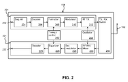
- Fig. 2 is a generalised schematic of the signal processing circuitry 154 that might be employed comprising, at a transmitter 201: a transmitter input 202, a segmenter 204, an encoder 206, for example a turbo encoder, a formatter 208, a modulator 210; a radio-frequency (RF) transmitter 212.
- a receiver 221 there is: a receiver output 222; a decoder 224, for example a turbo decoder, an equalizer 226, a demodulator 228; and a mixer 230.
- the transmitter 201 and receiver 221 there may also be hardware which is shared, such as: the antenna 152 for receiving the RF signals 122 from the communications network, timing and control circuitry 252, and an oscillator 254, along with transmitter-receiver switch 256.
- the transmitter 201 receives a digital data stream via transmitter input 202 and this data stream is fed to segmenter 204 where fixed-length data blocks of block size, K, are formed. These fixed-length data blocks are then passed to the encoder 206 which encodes the fixed length data blocks and sends the encoded data blocks successively as an encoded data stream to the formatter 208.
- the formatter 208 generates, at a prescribed time and with a prescribed amplitude, signal bursts, each comprising a series of waveforms. These bursts are passed to modulator 210 where each burst is modulated to RF frequency by mixing it with a carrier having a known frequency.
- the transmitter 201 then transmits each modulated burst as the RF signal 122 when the transmitter-receiver switch 256 connects the antenna 152 to the transmitter 201.
- the oscillator 254, which is connected to the modulator 210 tracks timing and is used by the modulator 210 to generate the carrier waveform.
- the timing and control circuitry 252 controls the formatting and timing of the bursts as generated by the formatter 208.
- the receiver 221 when the antenna 152 receives the RF signal 122 containing a burst and the radio frequency (RF) receiver / mixer 230 is connected to the antenna 152 via the switch 256, the received burst is amplified in the radio frequency (RF) receiver / mixer 230, and then demodulated in the demodulator 228 so as to remove the RF carrier.
- the equalizer 226 filters each demodulated burst to produce an enhanced digital signal which is next decoded by decoder 224.
- the decoder 224 comprises a concatenation of individual decoder elements (not shown) and an interleaver (see below). By using feedback from each decoder and passing data through the interleaver (see below), each received burst can be decoded, and can then be passed as needed through receiver output 222 to the processing circuitry 156 within the user equipment 150 for use and/or further processing.
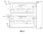
- Fig. 3 is a schematic of functional elements of the encoder 206, which may be implemented in hardware, or implemented in software executable on dedicated or shared processing circuitry, or implemented partially for certain elements in software, with other elements implemented hardware.
- the processing circuitry 156 may perform all or certain elements of the signal processing of the encoder 206 as described below.
- the signal processing circuitry 154 may comprise dedicated processing circuitry and memory for performing all or certain elements of the signal processing as described below.
- the example encoder 206 depicted in Fig. 3 includes two constituent encoder elements 301, 302. These encoder elements 301, 302 are both coupled to an interleaver 310. Each encoder element 301, 302 comprises, in the example shown in Fig. 3 : modular adders (or binary adders) ("+”); shift register delay elements (or “shift registers") ("D"); and a switch. As shown in the example of Fig. 3 , data, bits or information is/are output from each encoder element 301, 302 to a buffer 305. Data, bits or information, c k , is/are also output from encoder element 301 to the interleaver 310.
- Reordered data, bits or information, c' k are then output from the interleaver 310 to encoder element 302.
- the function of the encoder elements 301, 302 is described in one example according to the 3rd Generation Partnership Project (3GPP) (see 3GPP Technical Specification 36.212 v 11.0.0 as herein incorporated by reference, with particular reference to section 5.1.3.2).
- the interleaver employed in 3GPP TS 36.212 determines the order of output bits with respect to the input data, bits or information according to a pre-defined function.
- the data, bits or information input to the interleaver for example the interleaver 310 as depicted in Fig. 3
- K is the number of input bits, commonly referred to as the block size.
- the data, bits or information output from the interleaver for example the interleaver 310 as depicted in Fig. 3 , are denoted by c' 0 , c' 1 ,...,c' K- 1 .
- the order of bits in Eq. 1 is reversible in the sense that there can simply be a transformation from a given input bit location to an output bit location, and this transformation can be defined by an interleaver sequence function (see below) for reordering bits or symbols in a linear input bit or symbol sequence.
- an interleaver sequence function see below
- the reordering of bits is a subset of the reordering of symbols, whereby one or more bits constitute a symbol within a symbol sequence.
- the principles disclosed below concerning bit reordering are equally applicable to the more general scenario whereby symbols are reordered.
- a symbol may be a bit, e.g. a single bit, or it may be a group of one or more bits.
- An input symbol sequence may be reordered to generate a reordered output symbol sequence whereby the groups of one or more bits making up each symbol have been reordered.
- the location of a given symbol or bit in the input sequence may designated by or equate to an index, e.g. ⁇ (i), and the location of a given symbol or bit in the output sequence may be designated by or equate to an index, e.g. i. ⁇ (i) is an example of a value determined by an interleaver sequence function (see below).
- the input and output bits may simply be stored in a buffer 370 and bits are input in a linear fashion into the buffer and read out in an order according to the interleaver sequence function.
- the bits can also be input into the buffer in an order according to the interleaver sequence function and output in a linear fashion.
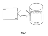
- the functional elements or logic in the example interleaver 310 are shown in Fig. 4 . These functional elements or logic may be implemented in dedicated hardware, or implemented in software executable on dedicated or shared processing circuitry, or implemented partially for certain elements in software, with other elements implemented hardware. These functional elements or logic implement the general process 500 described below with reference to Fig. 5 .
- the example interleaver 310 comprises a processing block 400 in communication with a memory 410 which stores parameters of an interleaver sequence function in quotient and remainder form.
- i is a linear input bit sequence location
- f 1 and f 2 are pre-defined parameters.
- K may be specified in terms of a parallelisation factor whereby interleaver processing within the processing block 400 can be used by P decoding processor elements (not shown) operating in parallel.
- P is defined as a power of 2, so in the case where the largest value of K is 6144, as specified in in 3GPP TS 36.212, Table 5.1.3-3 and section 5.1.2, and each decoding processor services, for example, 192 bits, the largest value of P will be 32, in which case the values for P for the values in 3GPP TS 36.212, Table 5.1.3-3 are from the set ⁇ 1, 2, 4, 8, 16, 32 ⁇ .
- Table 1 Exemplary values which might be stored in memory 410 and accessed from the memory 410 when deriving ⁇ (i), for example, are shown in the final column of Table 1 below: Table 1: Exemplary values of ⁇ K, f 1 [q f1 ,r f1 ], f 2 [q f2 ,r f2 ] ⁇ ⁇ K, f1, f2 ⁇ P wgs ⁇ K, f 1 [q f1 ,r f1 ], f 2 [q f2 ,r f2 ] ⁇ ⁇ 928,15, 58 ⁇ 8 116 ⁇ 928, [0,15], [0,58] ⁇ ⁇ 3008, 157, 188 ⁇ 32 94 ⁇ 3008, [1,63], [2,0] ⁇ ⁇ 6144,263,480 ⁇ 32 192 ⁇ 6144, [1,71], [2,96] ⁇
- the corresponding values of [q f1 ,r f1 ], [q f2 ,r f2 ] are selected from memory and may then be utilised to obtain interleaved bit sequence locations from non-interleaved/input bit sequence locations according to the general process described below.
- the functional elements or logic in the example interleaver 310 may be implemented in a computer readable medium, for example a non-transitory computer readable medium, having computer executable instructions stored thereon, which, when executed by a processor constituting the processing block 400, perform a general process 500 described below with reference to Fig. 5 .
- a suitable implementation may be to implement the processing block 400 in hardware components comprising processing elements, such as multiple -shift adder components.
- the "mod wgs " processing is commutative. The aforementioned application of the invention permits the processing to be broken down into its smallest parts and values to be obtained incrementally by keeping all internal result values within the ⁇ 0:wgs-1 ⁇ range.
- the interleaved [q] value output based on the interleaver sequence function in quotient-remainder form constitutes an interleaver shuffle index for mapping ⁇ (i) across all P processors.
- the interleaver 310 has performed reordering across its wgs range, and not K bits.
- the [q] output value permits the reordering performed for each processor to be mapped into a reordering for all K bits.
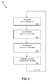
- the process 500 is depicted in which interleaved or re-ordered bit locations may be generated from successive bit locations of an input bit sequence or block utilising quotient and remainder ("[q,r]") values of parameters of the interleaver sequence function.
- the process 500 acquires, in step 510, [q f1 ,r f1 ] and [q f2 ,r f2 ] from memory for a particular K value, or wgs value based on P.
- an interleaved bit location is derived which can be output to memory, for example to a lookup table storing the correspondence between input bit sequence location and output bit location.
- the actual bit located at the input bit location is placed into an output register at the derived interleaved bit location.
- the interleaver sequence stored in memory can be used for both a read from a linear memory and as a write to a memory whose data is required to be stored in interleaved order (c.f. encoding and decoding of data).
- the same interleaver sequence function e.g. ⁇ (i)
- ⁇ (i) can be used to interleave and de-interleave.
- step 501 of P x ([q f1 ,r f1 ] x i) mod wgs at each step i ⁇ f 1 is compared with wgs . If i.f1 is larger than wgs , subtract wgs (perform modulation) and increment q by reducing to floor.
- wgs perform modulation
- the processing block 300 iterates starting from: 37 ⁇ [q: 2, r: 49] mod 144 ⁇ [q: 74, r: 1813] mod 144 which is reduced to floor as follows: ⁇ [q: 74+12, r: 85] where 12 is obtained from: 1813/144, and 85 is obtained from: 1813 mod 144 ⁇ [q: 86, r: 85] which corresponds to a calculation of: [q: 22, r:85]
- the i 2 mod wgs portion can be reduced to a single clock cycle operation by on the basis described below.
- [q f2 ,r f2 ] and their wgs for all interleaver parameters have a relationship that can be exploited.
- the processing block 300 iterates starting from: i ⁇ i ⁇ [q f2 ,r f2 ] mod wgs ⁇ ((i ⁇ i mod wgs ) ⁇ [q f2 ,r f2 ]) mod wgs ⁇ ((i ⁇ i mod cf) ⁇ [q f2 ,r f2 ] ⁇ mod wgs
- Each common family value has a corresponding i ⁇ i mod cf table (see Table 3 below).
- i ⁇ i mod cf ⁇ 0,1,4,9,16,25,36,1,16,33,4,25,0 ⁇ which, as for all the sets of values for each cf value, has a repeat sequence about its end value (i.e. final "0"), so cf /2 can be considered, and a reflection from the end of the sequence can be utilised.
- the functional elements or logic in the interleaver 310 which are thus necessary to relate the indices of the input bits, c k , to the corresponding indices of the output bits, c' k , can be significantly reduced vis-à-vis existing interleavers.
Landscapes
- Physics & Mathematics (AREA)
- Probability & Statistics with Applications (AREA)
- Engineering & Computer Science (AREA)
- Theoretical Computer Science (AREA)
- Mathematical Physics (AREA)
- Error Detection And Correction (AREA)
- Detection And Prevention Of Errors In Transmission (AREA)
Abstract
Description
- The present disclosure concerns an interleaver and interleaving process which employ an improved technique for deriving interleaved bit locations
- Interleaving is a process of reordering a sequence of bits, data, symbols or information which is contained in a data sequence, for example by reordering the bits, data, symbols or information in a predefined or pseudo-random manner. Apparatus which performs interleaving is herein referred to as an "interleaver".
- Turbo interleavers are interleavers which are used in the generation of turbo codes, and are used at the output of a first encoder element before the reordered data from the interleaver is further encoded by a second encoder element. Interleaving in the context of turbo encoding means that the separate encodings produced by the two encoder elements are generally uncorrelated. Thus, the outputs of the two encoder elements can then be combined to produce an encoded data sequence which has good error correction performance.
- Many interleavers determine the reordering sequence of their input bits, data, symbols or information based on an "interleaver sequence function" which is a mathematical function which takes the position of an input bit, data item, symbol or information block and derives a corresponding output position in the output stream of bits, data, symbols or information.
- In existing encoders and decoders, calculation of the interleaver sequence function involves an implementation in hardware or equivalent software. Often, the values that are being determined in the processing of the interleaver sequence function can become large. This means that the processing logic is relatively complex and thus the processing and calculation of interleaved bit sequences is demanding. This can increase circuit complexity, size and cost, as well as increase power consumption which, for mobile applications, can cause a reduction in battery life. It is thus desirable to reduce and simplify the logic required to implement the interleaver sequence function.
- Reference is made below to the accompanying drawings in which:
-
Fig. 1 is a schematic of a communication system according to the present disclosure; -
Fig. 2 is a schematic of signal processing circuitry which could be employed in the communication system ofFig. 1 ; -
Fig. 3 is a schematic of the functional components of an encoder which could be employed in the circuitry ofFig. 2 ; -
Fig. 3a is a schematic showing how bits or symbols according to the present disclosure may be reordered; -
Fig. 4 is a schematic of functional components of an interleaver of the present disclosure; and -
Fig. 5 is a flow diagram of steps which could be performed by an interleaver of the present disclosure. - Reference is made below to one or more particular examples which are not intended to be limiting on the scope of the disclosure.
- In a first aspect, a method of generating an interleaved symbol location from a linear symbol location of a symbol sequence may comprise: determining the interleaved symbol location based on an interleaver sequence function which relates a linear symbol location to the interleaved symbol location by: acquiring parameters of the interleaver sequence function in quotient and remainder form; calculating the interleaved symbol location by performing operations of the interleaver sequence function in quotient and remainder form; and outputting the determined interleaved symbol location.
- In performing the aforementioned method, the interleaver sequence function may be Π(i) = (f1 x i + f2 x i2) mod wgs, wherein i is the linear symbol location, and wgs, f1 and f2 are pre-defined constants. wgs, f1 and f2 may comprise one or more of the values defined according to Table 2 below.
- f1 and f2 may be expressed in quotient and remainder form, f1[q,r] and f2[q,r], where q is the quotient of f1 or f2 in integer form and r is the remainder of f1 or f2 in integer form with respect to wgs. f1 and f2 may be stored in quotient and remainder form in memory, and obtained therefrom. Multiple values for f1[q,r] and f2[q,r] in quotient and remainder form are stored in and acquired from memory. wgs may equate to K / P, wherein P is a parallelisation factor and K is code block size of the symbol sequence.
- The step of calculating may comprise at least one lookup operation and at least one iterative shift-add operation. Moreover, determining the interleaved symbol location may be an iterative determination based on one or more successive symbol locations and their one or more corresponding determined interleaved symbol locations.
- In a second aspect, a non-transitory computer readable medium has computer executable instructions stored thereon, when executed, perform the aforementioned method.
- In a fourth aspect, an interleaver for generating an interleaved symbol location from a linear symbol location of a symbol sequence may comprise: a processing circuit configured to determine the interleaved symbol location based on an interleaver sequence function which relates a linear symbol location to the interleaved symbol location by: acquiring parameters of the interleaver sequence function in quotient and remainder form; and calculating the interleaved symbol sequence location by performing operations of the interleaver sequence function in quotient and remainder form, wherein the processing circuit is further configured to output the determined interleaved symbol location.
- The interleaver can perform interleaving and de-interleaving operations since the interleaver sequence function may be reversible. This is to say a linear symbol sequence input to the interleaver can be reordered such that an interleaved symbol sequence is output, or a interleaved input sequence input to the interleaver can be reordered such that a linear symbol sequence is output.
- For the aforementioned interleaver, the interleaver sequence function may be Π(i) = (f1 x i + f2 x i2) mod wgs, wherein i is the linear symbol location, and wgs, f1 and f2 are pre-defined constants. wgs, f1 and f2 may comprise one or more of the values defined according to Table 2 below. f1 and f2 may be expressed in quotient and remainder form, f1[q,r] and f2[q,r], where q is the quotient off or f2 in integer form and r is the remainder off or f2 in integer form with respect to wgs. f1 and f2 may be stored in quotient and remainder form in memory, and obtained therefrom. Multiple values for f1[q,r] and f2[q,r] in quotient and remainder form are stored in and acquired from memory. wgs may equate to K / P, wherein P is a parallelisation factor and K is code block size of the symbol sequence.
- The processing circuit may be configured to perform at least one lookup operation and at least one iterative shift-add operation during calculation of the interleaved symbol sequence index. These operations may be performed using quotient and remainder operations.
- The processor may be configured to determine the interleaved symbol location by performing an iterative determination based on one or more preceding successive symbol locations and their one or more corresponding determined interleaved symbol locations.
- In a fourth aspect, a device comprising the aforementioned interleaver may store multiple values for f1[q,r] and f2[q,r] in quotient and remainder form, wherein the processing circuit is configured to acquire values for f1[q,r] and f2[q,r] in quotient and remainder form from the memory.
- The device may comprise an encoder configured for encoding a symbol sequence and perform an interleaving operation by successively passing a linear symbol location of the symbol sequence to the aforementioned interleaver and thereby obtain a corresponding interleaved symbol location from the interleaver.
- The device may comprise a decoder which may be configured for decoding an interleaved symbol sequence and perform a de-interleaving operation by successively passing an interleaved symbol location of the symbol sequence to the aforementioned interleaver and thereby obtain a corresponding linear symbol location from the interleaver.
- In a fifth aspect, user equipment for use in a telecommunications network may comprise the aforementioned device.
- In the aforementioned interleaver and method, each symbol may comprise one or more bits, may comprise a single bit, or may be a single bit. Each symbol sequence (input or output) may be a bit sequence and each symbol location may be a bit location. The reference to a symbol or bit location may be a reference to a symbol or bit index respectively within the corresponding symbol or bit sequence. The linear sequence may be defined as a non-interleaved sequence and be the sequence that is input or output from the interleaver.
-
Fig. 1 is an example of acommunication system 100 which could employ the present invention. Thecommunication system 100 comprises user equipment (UE) 150 which may be a communication device, such as a mobile device or phone, portable computing device, e.g. laptop or tablet device, or any other device which is adapted to communicate with thesystem 100. The user equipment (UE) 150 comprisesprocessing circuitry 156 in communication withmemory 158. Theprocessing circuitry 156 is also in communication withsignal processing circuitry 154 which is connected toantenna 152. Theuser equipment 150 may also include many other commonplace features which are likely to well-understood by the skilled person. These commonplace features are not shown inFig. 1 since they are not the direct subject of the present invention, but may include a display screen, keypad or keyboard, touchscreen, power supply, such as a battery, input/output interfaces. Such commonplace features may be directly or indirectly connected to each other, to theprocessing circuitry 156,memory 158 and/orsignal processing circuitry 154, and be in direct or indirect communication with each other, theprocessing circuitry 156,memory 158 and/orsignal processing circuitry 154. - The
communication system 100 also comprises aremote station 160, which may be a mobile station (MS), such as a mobile base station or any other device which is capable of communicating within thesystem 100 and with theuser equipment 150. Thestation 160 may comprisestation antenna 162 and signal processing and control circuitry (not shown), which may be directly or indirectly connected to thestation antenna 162, and which may be similar or identical to the components of the user equipment as herein described. - Radio frequency (RF)
signals 122 are generated by theuser equipment 150 and thestation 160 and pass between each other via theantenna 152 andstation antenna 162, thereby permitting bi-directional communication between theuser equipment 150 and thestation 160. The RF signals 122 are modulated or demodulated by theuser equipment 150 and/or thestation 160 according to one or more modulation/demodulation schemes, which permits data, for example digital data, to be transmitted between thestation 160 and theuser equipment 150. The modulation schemes implemented by thecommunication system 100 including theuser equipment 150 andstation 160 may conform to one or more of the schemes defined by Global System for Mobile Communications (GSM), 3rd Generation (3G) mobile communication, 3rd Generation Partnership Project (3GPP) and Long Term Evolution (LTE). The resulting communication network which is formed by the user equipment 150 (or a plurality thereof) and the station 160 (or a plurality thereof) may be a cellular communication network, such as a cellular network conforming to one or more of GSM, 3G, 3GPP and LTE. -
Fig. 2 is a generalised schematic of thesignal processing circuitry 154 that might be employed comprising, at a transmitter 201: atransmitter input 202, asegmenter 204, anencoder 206, for example a turbo encoder, aformatter 208, amodulator 210; a radio-frequency (RF)transmitter 212. In addition, at areceiver 221, there is: areceiver output 222; adecoder 224, for example a turbo decoder, anequalizer 226, ademodulator 228; and amixer 230. - For both the
transmitter 201 andreceiver 221, there may also be hardware which is shared, such as: theantenna 152 for receiving the RF signals 122 from the communications network, timing andcontrol circuitry 252, and anoscillator 254, along with transmitter-receiver switch 256. - The
transmitter 201 receives a digital data stream viatransmitter input 202 and this data stream is fed to segmenter 204 where fixed-length data blocks of block size, K, are formed. These fixed-length data blocks are then passed to theencoder 206 which encodes the fixed length data blocks and sends the encoded data blocks successively as an encoded data stream to theformatter 208. Theformatter 208 generates, at a prescribed time and with a prescribed amplitude, signal bursts, each comprising a series of waveforms. These bursts are passed to modulator 210 where each burst is modulated to RF frequency by mixing it with a carrier having a known frequency. Thetransmitter 201 then transmits each modulated burst as theRF signal 122 when the transmitter-receiver switch 256 connects theantenna 152 to thetransmitter 201. Theoscillator 254, which is connected to the modulator 210 tracks timing and is used by themodulator 210 to generate the carrier waveform. The timing andcontrol circuitry 252 controls the formatting and timing of the bursts as generated by theformatter 208. - For the
receiver 221, when theantenna 152 receives the RF signal 122 containing a burst and the radio frequency (RF) receiver /mixer 230 is connected to theantenna 152 via theswitch 256, the received burst is amplified in the radio frequency (RF) receiver /mixer 230, and then demodulated in thedemodulator 228 so as to remove the RF carrier. Theequalizer 226 filters each demodulated burst to produce an enhanced digital signal which is next decoded bydecoder 224. - The
decoder 224 comprises a concatenation of individual decoder elements (not shown) and an interleaver (see below). By using feedback from each decoder and passing data through the interleaver (see below), each received burst can be decoded, and can then be passed as needed throughreceiver output 222 to theprocessing circuitry 156 within theuser equipment 150 for use and/or further processing. -
Fig. 3 is a schematic of functional elements of theencoder 206, which may be implemented in hardware, or implemented in software executable on dedicated or shared processing circuitry, or implemented partially for certain elements in software, with other elements implemented hardware. Theprocessing circuitry 156 may perform all or certain elements of the signal processing of theencoder 206 as described below. Alternatively, or in addition, thesignal processing circuitry 154 may comprise dedicated processing circuitry and memory for performing all or certain elements of the signal processing as described below. - The
example encoder 206 depicted inFig. 3 includes twoconstituent encoder elements encoder elements interleaver 310. Eachencoder element Fig. 3 : modular adders (or binary adders) ("+"); shift register delay elements (or "shift registers") ("D"); and a switch. As shown in the example ofFig. 3 , data, bits or information is/are output from eachencoder element buffer 305. Data, bits or information, ck , is/are also output fromencoder element 301 to theinterleaver 310. Reordered data, bits or information, c'k , are then output from theinterleaver 310 toencoder element 302. The function of theencoder elements - The interleaver employed in 3GPP TS 36.212 determines the order of output bits with respect to the input data, bits or information according to a pre-defined function. In particular, the relationship between the input and output bits can be defined by the following expression:

interleaver 310 as depicted inFig. 3 , are denoted by c 0, c 1, ..., c K-1, and where K is the number of input bits, commonly referred to as the block size. The data, bits or information output from the interleaver, for example theinterleaver 310 as depicted inFig. 3 , are denoted by c' 0 , c' 1 ,...,c' K-1 . - The order of bits in Eq. 1 is reversible in the sense that there can simply be a transformation from a given input bit location to an output bit location, and this transformation can be defined by an interleaver sequence function (see below) for reordering bits or symbols in a linear input bit or symbol sequence. In the specific examples described below, reference is made to the reordering of individual bits in a bit sequence. However, it will be appreciated that the reordering of bits is a subset of the reordering of symbols, whereby one or more bits constitute a symbol within a symbol sequence. Hence, the principles disclosed below concerning bit reordering are equally applicable to the more general scenario whereby symbols are reordered. According to the invention as defined by the claims, a symbol may be a bit, e.g. a single bit, or it may be a group of one or more bits. An input symbol sequence may be reordered to generate a reordered output symbol sequence whereby the groups of one or more bits making up each symbol have been reordered. The location of a given symbol or bit in the input sequence may designated by or equate to an index, e.g. Π(i), and the location of a given symbol or bit in the output sequence may be designated by or equate to an index, e.g. i. Π(i) is an example of a value determined by an interleaver sequence function (see below).
- In an implementation of the interleaver (see
Fig. 3a ) for encoding, the input and output bits may simply be stored in a buffer 370 and bits are input in a linear fashion into the buffer and read out in an order according to the interleaver sequence function. In an implementation of the interleaver (seeFig. 3b ) for decoding, the bits can also be input into the buffer in an order according to the interleaver sequence function and output in a linear fashion. - The relationship between the indices of the input and output bits can be determined according to 3GPP TS 36.212 from the following expression:

where the parameters ƒ 1 and ƒ 2 are defined according to the block size K and are summarized in Table 5.1.3-3 of 3GPP TS 36.212, which is herein incorporated by reference. - In existing encoders and decoders, calculation of (ƒ 1 · i + ƒ 2 · i 2) is implemented in hardware, or in equivalent software, employing three multiplier elements and one adder element. Due to the values of ƒ 1 and ƒ 2 and block size K defined according to in Table 5.1.3-3 of 3GPP TS 36.212, the result of (ƒ 1 ·i + ƒ 2 · i2 ) can be very large, e.g. greater than 30 bits, perhaps, 31, 32, 33, 34 or 35 bits in length. For example. from Table 5.1.3-3 of 3GPP TS 36.212, for K=5248, f1= 113 & f2 = 902 and a max value of i = 5247:

where 26566614009 is a large number which requires 35 bits to represent it. The application of mod K to the large value which is obtained from (ƒ 1 · i + ƒ 2 · i 2) thus involves considerable divider logic which can be complex to implement and inefficient in processing. - The functional elements or logic in the
example interleaver 310 are shown inFig. 4 . These functional elements or logic may be implemented in dedicated hardware, or implemented in software executable on dedicated or shared processing circuitry, or implemented partially for certain elements in software, with other elements implemented hardware. These functional elements or logic implement thegeneral process 500 described below with reference toFig. 5 . - As shown in
Fig. 4 , theexample interleaver 310 comprises aprocessing block 400 in communication with amemory 410 which stores parameters of an interleaver sequence function in quotient and remainder form. For example, the interleaver sequence function may be Π(i) = (f1 x i + f2 x i2) mod K, as, for example, defined in 3GPP TS 36.212 section 5.1.3.2.3, in which case the parameters f1, f2 and/or K may be stored in the memory in quotient and remainder form. Also, i is a linear input bit sequence location, and K (block size), f1 and f2 are pre-defined parameters. - In particular, K may be specified in terms of a parallelisation factor whereby interleaver processing within the
processing block 400 can be used by P decoding processor elements (not shown) operating in parallel. P is defined as a power of 2, so in the case where the largest value of K is 6144, as specified in in 3GPP TS 36.212, Table 5.1.3-3 and section 5.1.2, and each decoding processor services, for example, 192 bits, the largest value of P will be 32, in which case the values for P for the values in 3GPP TS 36.212, Table 5.1.3-3 are from the set {1, 2, 4, 8, 16, 32}. Since the decoding processor elements can operate in parallel, this means that the interleaver bit sequence expression can be written as Π(i) = (f1 x i + f2 x i2) mod wgs, where wgs is the window group size defined as K / P. - The values f1, f2 and K may thus be expressed and/or directly stored in the
memory 410 in terms of K (or P and wgs), [qf1,rf1], [qf2,rf2] (generalised as fx[qfx,rfx]), where:

- Exemplary values which might be stored in
memory 410 and accessed from thememory 410 when deriving Π(i), for example, are shown in the final column of Table 1 below:Table 1: Exemplary values of {K, f1[qf1,rf1], f2[qf2,rf2]} {K, f1, f2} P wgs {K, f1[qf1,rf1], f2[qf2,rf2]} {928,15, 58} 8 116 {928, [0,15], [0,58]} {3008, 157, 188} 32 94 {3008, [1,63], [2,0]} {6144,263,480} 32 192 {6144, [1,71], [2,96]} - All applicable values of {K, [qf1,rf1], [qf2,rf2]} which may be stored in
memory 410 and accessed from thememory 410 when deriving Π(i), for example, are shown in the final column of Table 2 which is below. - For an information bit sequence or block having a particular block size, K, corresponding to the number of bits in the sequence or block, the corresponding values of [qf1,rf1], [qf2,rf2] are selected from memory and may then be utilised to obtain interleaved bit sequence locations from non-interleaved/input bit sequence locations according to the general process described below. The functional elements or logic in the
example interleaver 310 may be implemented in a computer readable medium, for example a non-transitory computer readable medium, having computer executable instructions stored thereon, which, when executed by a processor constituting theprocessing block 400, perform ageneral process 500 described below with reference toFig. 5 . However, a suitable implementation may be to implement theprocessing block 400 in hardware components comprising processing elements, such as multiple -shift adder components. - For the specific example where the interleaver sequence function, Π(i) = (f1 x i + f2 x i2) mod K, since turbo decoding processing is carried our across P parallel decoding processors of length wgs, where wgs = K/P, the interleaver derivation for each processor can be said to be Π(i) = (f1 x i + f2 x i2) mod wgs. All processors, P may use and process precisely the same linear i location index and return the same interleaved Π(i), index. As a result, there may only be one
interleaver processing block 400 to service all of the P decoding processors. Since all processors, P, use the same indexes, their data memory accesses can all use the same memory address from onesingle memory 410. - For this specific example, applying the general principles of the invention, the interleaver quotient-remainder parameters from
memory 410 are obtained for a particular value of wgs (where wgs = K / P):
- In all quotient-remainder ("[q,r]") processing, all [q,r] balances may generally be maintained. The remainder ("[r]") term should generally remain in the {0:wgs-1} range. However the quotient ("[q]") value can increase in value, but may be kept below mod P since it has the effect of multiplexing the interleaved data from memory back to a target processor. This is achieved because the final [q] value provides information about how to configure an external shuffle matrix for bit re-ordering, for example in an LTE interleaver. In particular, the interleaved [q] value output based on the interleaver sequence function in quotient-remainder form constitutes an interleaver shuffle index for mapping Π(i) across all P processors. In this regard, it should be recalled that the
interleaver 310 has performed reordering across its wgs range, and not K bits. Hence, the [q] output value permits the reordering performed for each processor to be mapped into a reordering for all K bits. - With reference to
Fig. 5 , theprocess 500 is depicted in which interleaved or re-ordered bit locations may be generated from successive bit locations of an input bit sequence or block utilising quotient and remainder ("[q,r]") values of parameters of the interleaver sequence function. In general, theprocess 500 acquires, instep 510, [qf1,rf1] and [qf2,rf2] from memory for a particular K value, or wgs value based on P. Theprocess 500 then calculates Π(i) = ([qf1,rf1] x i + [qf2,rf2] x i2) mod wgs, for each non-zero bit at location i, whereby there are two determinations, specifically: (i) determination ([qf1,rf1] x i) mod wgs (step 501); and (ii) determination of ([qf2,rf2] x i2) mod wgs (step 502); and (iii) followed by a sum of the results of (i) and (ii) (step 503) to generate an output which is an interleaved bit location. - According to step 503, an interleaved bit location is derived which can be output to memory, for example to a lookup table storing the correspondence between input bit sequence location and output bit location. Alternatively, the actual bit located at the input bit location is placed into an output register at the derived interleaved bit location. When all the bits in the input bit sequence (up to a block size, K) have been reordered, or their interleaved positions determined, the
process 500 terminates. At this point, the entire interleaved bit sequence from the output register is output, or, if not already generated, is generated based on the interleaved locations located in the lookup table (seeFig. 3a above). The interleaver sequence stored in memory (either directly by storage of the bit index, or by virtue of the location of the data itself) can be used for both a read from a linear memory and as a write to a memory whose data is required to be stored in interleaved order (c.f. encoding and decoding of data). By this arrangement, the same interleaver sequence function, e.g. Π(i), can be used to interleave and de-interleave. - An example application of the
process 500 for {K, f1, f2} being {4608, 337, 480} is now described where P=32. Hence, wgs=144. Thus, {K, [qf1,rf1], [qf2,rf2]} for this particular example is {4608, [2,49], [3, 48]} (see Table 2 below). It should be recalled that {i, D(i)} can be any value from 0 to 143 for wgs=144. Π(i) is always returned in the [q,r] format. [r] is used because that is the local interleaved address, i.e. it provides the result, and [q] permits the higher level wgs-to-K shuffle to occur when utilising P processors. The example process disclosed below operates in the [q,r] domain from the outset, rather than transforming at the end, as in conventional interleavers. - For the determination in
step 501 of P x ([qf1,rf1] x i) mod wgs, at each step i·f1 is compared with wgs. If i.f1 is larger than wgs, subtract wgs (perform modulation) and increment q by reducing to floor. According to an example of the invention, e.g. for i = 37, the processing block 300 iterates starting from:
37 · [q: 2, r: 49] mod 144
→ [q: 74, r: 1813] mod 144
which is reduced to floor as follows:
→ [q: 74+12, r: 85]
where 12 is obtained from: 1813/144, and 85 is obtained from: 1813 mod 144
→ [q: 86, r: 85]
which corresponds to a calculation of:
[q: 22, r:85] - For comparison, the direct approach would have yielded:
37·337 mod 144
→ 12469 mod 144
→ [q: 22, r: 85] - For the determination in
step 502 of P x ([qf2,rf2] x i2) mod wgs, the i2 mod wgs portion can be reduced to a single clock cycle operation by on the basis described below. [qf2,rf2] and their wgs for all interleaver parameters have a relationship that can be exploited. - According to the example for i = 37, the processing block 300 iterates starting from:
i·i·[qf2,rf2] mod wgs
→ ((i·i mod wgs) · [qf2,rf2]) mod wgs
→ ((i·i mod cf)· [qf2,rf2]} mod wgs - This calculation can be performed by recalling that {K,f1,f2} is {4608, 337, 480}, where 96 now factors into both 4608 and 480, and 4608 is 96 x 48, where this 48 value defines which common family that K = 4608 falls into.
- There are only six common family values for the values of K, P and wgs in 3GPP TS 36.212, Table 5.1.3-3 which are {64, 48, 40, 112, 18, 54} (see Table 3 below).
- Each common family value has a corresponding i·i mod cf table (see Table 3 below). For example, for cf = 48, i·i mod cf = {0,1,4,9,16,25,36,1,16,33,4,25,0} which, as for all the sets of values for each cf value, has a repeat sequence about its end value (i.e. final "0"), so cf /2 can be considered, and a reflection from the end of the sequence can be utilised.
- Thus, in determining 37 · 37 mod 48, i=37 can be used as an index into the table for the cf = 48 value. Since, as stated above the sequence reflects, mod (48 / 2 = 24) cen be calculated. Hence, 37 mod 24 is 13, which yields 25 for i·i mod cf since the 13th element in the table for cf = 48 is 25 (reflected back and the index count has started from zero).
- Thus:
((i·i mod cf)· [qf2,rf2]} mod wgs
→ 25 · [qf2,rf2] mod wgs
→ 25 · [q:3, r:48] mod 144
Theprocessing block 400 then iterates 25 · [q:3, r:48] mod 144 as:
[q:75, r:1200] mod 144
→ [q:75+8, r:48]
→ [q:19, r:48]
where q has been reduced mod 32 and 8 is obtained from 1200/144 and 48 is obtained from 1200 mod 144. - For comparison, the direct approach would have yielded:
i·i·f2 mod wgs
→ 657120 mod 144
→ [q:4563, r:48]
→ [q:19, r:48] - It can thus be seen that the direct approach for the determination in the examples of
steps process 500 performed by the processing block 400 (not limited to the above-mentioned specific example) is reduced to one or more lookups frommemory 410, and one or more iterative shift-add operations, by storing the {f1,f2} parameters as their mod wgs [q,r] equivalents inmemory 410, and obtaining these {f1,f2} in their quotient-remainder form for a given value of K when performing interleaving using the interleaver sequence function. This significantly reduces the hardware both in terms of the operations performed and the bit widths of all on-going calculations. It also significantly reduces the time taken to compute the interleaved bit sequence values. In essence, through using this technique, the architecture is able to step towards a result, rather than over-calculate interim values and then trimming them away (with divide functions), as per the direct, conventional approach. - Applying the aforementioned process, the functional elements or logic in the
interleaver 310 which are thus necessary to relate the indices of the input bits, ck , to the corresponding indices of the output bits, c'k, can be significantly reduced vis-à-vis existing interleavers. - It will be appreciated that the invention has been described above by way of examples, and that modifications departing from the examples may be applicable within the scope of the invention, which is defined by the appendant claims.
Table 2: Values of {K, [qf1,rf1], [qf2,rf2]} for determining Π(i) = (f1 x i + f2 x i2) mod K {K, f1, f2} P wgs {K, [qf1,r f1 ], [qf2,rf2]} {40, 3, 10} 1 40 {40, [0,3], [0,10]} {48, 7, 12} 1 48 {48, [0,7], [0,12]} {56, 19, 42} 1 56 {56, [0,19], [0,42]} {64, 7, 16} 1 64 {64, [0,7], [0,16]} {72, 7, 18} 1 72 {72, [0,7], [0,18]} {80, 11, 20} 1 80 {80, [0,11], [0,20]} {88, 5, 22} 1 88 {88, [0,5], [0,22]} {96, 11, 24} 1 96 {96, [0,11], [0,24]} {104, 7, 26} 1 104 {104, [0,7], [0,26]} {112, 41, 84} 1 112 {112, [0,41], [0,84]} {120, 103, 90} 1 120 {120, [0,103], [0,90]} {128, 15, 32} 2 64 {128, [0,15], [0,32]} {136, 9, 34} 2 68 {136, [0,9], [0,34]} {144, 17, 108} 2 72 {144, [0,17], [1,36]} {152, 9, 38} 2 76 {152, [0,9], [0,38]} {160, 21, 120} 2 80 {160, [0,21], [1,40]} {168, 101, 84} 2 84 {168, [1,17], [1,0]} {176, 21, 44} 2 88 {176, [0,21], [0,44]} {184, 57, 46} 2 92 {184, [0,57], [0,46]} {192, 23, 48} 2 96 {192, [0,23], [0,48]} {200, 13, 50} 2 100 {200, [0,13], [0,50]} {208, 27, 52} 2 104 {208, [0,27], [0,52]} {216, 11, 36} 2 108 {216, [0,11], [0,36]} {224, 27, 56} 2 112 {224, [0,27], [0,56]} {232, 85, 58} 2 116 {232, [0,85], [0,58]} {240, 29, 60} 2 120 {240, [0,29], [0,60]} {248, 33, 62} 2 124 {248, [0,33], [0,62]} {256, 15, 32} 4 64 {256, [0,15], [0,32]} {264, 17, 198} 4 66 {264, [0,17], [3,0]} {272, 33, 68} 4 68 {272, [0,33], [1,0]} {280, 103, 210} 4 70 {280, [1,33], [3,0]} {288, 19, 36} 4 72 {288, [0,19], [0,36]} {296, 19, 74} 4 74 {296, [0,19], [1,0]} {304, 37, 76} 4 76 {304, [0,37], [1,0]} {312, 19, 78} 4 78 {312, [0,19], [1,0]} {320, 21, 120} 4 80 {320, [0,21], [1,40]} {328, 21, 82} 4 82 {328, [0,21], [1,0]} {336, 115, 84} 4 84 {336, [1,31], [1,0]} {344, 193, 86} 4 86 {344, [2,21], [1,0]} {352, 21, 44} 4 88 {352, [0,21], [0,44]} {360, 133, 90} 4 90 {360, [1,43], [1,0]} {368, 81, 46} 4 92 {368, [0,81], [0,46]} {376, 45, 94} 4 94 {376, [0,45], [1,0]} {384, 23, 48} 4 96 {384, [0,23], [0,48]} {392, 243, 98} 4 98 {392, [2,47], [1,0]} {400, 151, 40} 4 100 {400, [1,51], [0,40]} {408, 155, 102} 4 102 {408, [1,53], [1,0]} {416, 25, 52} 4 104 {416, [0,25], [0,52]} {424, 51, 106} 4 106 {424, [0,51], [1,0]} {432, 47, 72} 4 108 {432, [0,47], [0,72]} {440, 91, 110} 4 110 {440, [0,91], [1,0]} {448, 29, 168} 4 112 {448, [0,29], [1,56]} {456, 29, 114} 4 114 {456, [0,29], [1,0]} {464, 247, 58} 4 116 {464, [2,15], [0,58]} {472, 29, 118} 4 118 {472, [0,29], [1,0]} {480, 89, 180} 4 120 {480, [0,89], [1,60]} {488, 91, 122} 4 122 {488, [0,91], [1,0]} {496, 157, 62} 4 124 {496, [1,33], [0,62]} {504, 55, 84} 4 126 {504, [0,55], [0,84]} {512, 31, 64} 8 64 {512, [0,31], [1,0]} {528, 17, 66} 8 66 {528, [0,17], [1,0]} {544, 35, 68} 8 68 {544, [0,35], [1,0]} {560, 227, 420} 8 70 {560, [3,17], [6,0]} {576, 65, 96} 8 72 {576, [0,65], [1,24]} {592, 19, 74} 8 74 {592, [0,19], [1,0]} {60S, 37, 76} 8 76 {608, [0,37], [1,0]} {624, 41, 234} 8 78 {624, [0,41], [3,0]} {640, 39, 80} 8 80 {640, [0,39], [1,0]} {656, 185, 82} 8 82 {656, [2,21], [1,0]} {672, 43, 252} 8 84 {672, [0,43], [3,0]} {688, 21, 86} 8 86 {688, [0,21], [1,0]} {704, 155, 44} 8 88 {704, [1,67], [0,44]} {720, 79, 120} 8 90 {720, [0,79], [1,30]} {736, 139, 92} 8 92 {736, [1,47], [1,0]} {752, 23, 94} 8 94 {752, [0,23], [1,0]} {768, 217, 48} 8 96 {768, [2,25], [0,48]} {784, 25, 98} 8 98 {784, [0,25], [1,0]} {800, 17, 80} 8 100 {800, [0,17], [0,80]} {816, 127, 102} 8 102 {816, [1,25], [1,0]} {832, 25, 52} 8 104 {832, [0,25], [0,52]} {848, 239, 106} 8 106 {848, [2,27], [1,0]} {864, 17, 48} 8 108 {864, [0,17], [0,48]} {880, 137, 110} 8 110 {880, [1,27], [1,0]} {896, 215, 112} 8 112 {896, [1,103], [1,0]} {912, 29, 114} 8 114 {912, [0,29], [1,0]} {928, 15, 58} 8 116 {928, [0,15], [0,58]} {944, 147, 118} 8 118 {944, [1,29], [1,0]} {960, 29, 60} 8 120 {960, [0,29], [0,60]} {976, 59, 122} 8 122 {976, [0,59], [1,0]} {992, 65, 124} 8 124 {992, [0,65], [1,0]} {1008, 55, 84} 8 126 {1008, [0,55], [0,84]} {1024, 31, 64} 16 64 {1024, [0,31], [1,0]} {1056, 17, 66} 16 66 {1056, [0,17], [1,0]} {1088, 171, 204} 16 68 {1088, [2,35], [3,0]} {1120, 67, 140} 16 70 {1120, [0,67], [2,0]} {1152, 35, 72} 16 72 {1152, [0,35], [1,0]} {1184, 19, 74} 16 74 {1184, [0,19], [1,0]} {1216, 39, 76} 16 76 {1216, [0,39], [1,0]} {1248, 19, 78} 16 78 {1248, [0,19], [1,0]} {1280, 199, 240} 16 80 {1280, [2,39], [3,0]} {1312, 21, 82} 16 82 {1312, [0,21], [1,0]} {1344, 211, 252} 16 84 {1344, [2,43], [3,0]} {1376, 21, 86} 16 86 {1376, [0,21], [1,0]} {1408, 43, 88} 16 88 {1408, [0,43], [1,0]} {1440, 149, 60} 16 90 {1440, [1,59], [0,60]} {1472, 45, 92} 16 92 {1472, [0,45], [1,0]} {1504, 49, 846} 16 94 {1504, [0,49], [9,0]} {1536, 71, 48} 16 96 {1536, [0,71], [0,48]} {1568, 13, 28} 16 98 {1568, [0,13], [0,28]} {1600, 17, 80} 16 100 {1600, [0,17], [0,80]} {1632, 25, 102} 16 102 {1632, [0,25], [1,0]} {1664, 183, 104} 16 104 {1664, [1,79], [1,0]} {1696, 55, 954} 16 106 {1696, [0,55], [9,0]} {1728, 127, 96} 16 108 {1728, [1,19], [0,96]} {1760, 27, 110} 16 110 {1760, [0,27], [1,0]} {1792, 29, 112} 16 112 {1792, [0,29], [1,0]} {1824, 29, 114} 16 114 {1824, [0,29], [1,0]} {1856, 57, 116} 16 116 {1856, [0,57], [1,0]} {1888, 45, 354} 16 118 {1888, [0,45], [3,0]} {1920, 31, 120} 16 120 {1920, [0,31], [1,0]} {1952, 59, 610} 16 122 {1952, [0,59], [5,0]} {1984, 185, 124} 16 124 {1984, [1,61], [1,0]} {2016, 113, 420} 16 126 {2016, [0,113], [3,42]} {2048, 31, 64} 32 64 {2048, [0,31], [1,0]} {2112, 17, 66} 32 66 {2112, [0,17], [1,0]} {2176, 171, 136} 32 68 {2176, [2,35], [2,0]} {2240, 209, 420} 32 70 {2240, [2,69], [6,0]} {2304, 253, 216} 32 72 {2304, [3,37], [3,0]} {2368, 367, 444} 32 74 {2368, [4,71], [6,0]} {2432, 265, 456} 32 76 {2432, [3,37], [6,0]} {2496, 181, 468} 32 78 {2496, [2,25], [6,0]} {2560, 39, 80} 32 80 {2560, [0,39], [1,0]} {2624, 27, 164} 32 82 {2624, [0,27], [2,0]} {2688, 127, 504} 32 84 {2688, [1,43], [6,0]} {2752, 143, 172} 32 86 {2752, [1,57], [2,0]} {2816, 43, 88} 32 88 {2816, [0,43], [1,0]} {2880, 29, 300} 32 90 {2880, [0,29], [3,30]} {2944, 45, 92} 32 92 {2944, [0,45], [1,0]} {3008, 157, 188} 32 94 {3008, [1,63], [2,0]} {3072, 47, 96} 32 96 {3072, [0,47], [1,0]} {3136, 13, 28} 32 98 {3136, [0,13], [0,28]} {3200, 111, 240} 32 100 {3200, [1,11], [2,40]} {3264, 443, 204} 32 102 {3264, [4,35], [2,0]} {3328, 51, 104} 32 104 {3328, [0,51], [1,0]} {3392, 51, 212} 32 106 {3392, [0,51], [2,0]} {3456, 451, 192} 32 108 {3456, [4,19], [1,84]} {3520, 257, 220} 32 110 {3520, [2,37], [2,0]} {3584, 57, 336} 32 112 {3584, [0,57], [3,0]} {3648, 313, 228} 32 114 {3648, [2,85], [2,0]} {3712, 271, 232} 32 116 {3712, [2,39], [2,0]} {3776, 179, 236} 32 118 {3776, [1,61], [2,0]} {3840, 331, 120} 32 120 {3840, [2,91], [1,0]} {3904, 363, 244} 32 122 {3904, [2,119], [2,0]} {3968, 375, 248} 32 124 {3968, [3,3], [2,0]} {4032, 127, 168} 32 126 {4032, [1,1], [1,42]} {4096, 31, 64} 32 128 {4096, [0,31], [0,64]} {4160, 33, 130} 32 130 {4160, [0,33], [1,0]} {4224, 43, 264} 32 132 {4224, [0,43], [2,0]} {4288, 33, 134} 32 134 {4288, [0,33], [1,0]} {4352, 477, 408} 32 136 {4352, [3,69], [3,0]} {4416, 35, 138} 32 138 {4416, [0,35], [1,0]} {4480, 233, 280} 32 140 {4480, [1,93], [2,0]} {4544, 357, 142} 32 142 {4544, [2,73], [1,0]} {4608, 337, 480} 32 144 {4608, [2,49], [3,48]} {4672, 37, 146} 32 146 {4672, [0,37], [1,0]} {4736, 71, 444} 32 148 {4736, [0,71], [3,0]} {4800, 71, 120} 32 150 {4800, [0,71], [0,120]} {4864, 37, 152} 32 152 {4864, [0,37], [1,0]} {4928, 39, 462} 32 154 {4928, [0,39], [3,0]} {4992, 127, 234} 32 156 {4992, [0,127], [1,78]} {5056, 39, 158} 32 158 {5056, [0,39], [1,0]} {5120, 39, 80} 32 160 {5120, [0,39], [0,80]} {5184, 31, 96} 32 162 {5184, [0,31], [0,96]} {5248, 113, 902} 32 164 {5248, [0,113], [5,82]} {5312, 41, 166} 32 166 {5312, [0,41], [1,0]} {5376, 251, 336} 32 168 {5376, [1,83], [2,0]} {5440, 43, 170} 32 170 {5440, [0,43], [1,0]} {5504, 21, 86} 32 172 {5504, [0,21], [0,86]} {5568, 43, 174} 32 174 {5568, [0,43], [1,0]} {5632, 45, 176} 32 176 {5632, [0,45], [1,0]} {5696, 45, 178} 32 178 {5696, [0,45], [1,0]} {5760, 161, 120} 32 180 {5760, [0,161], [0,120]} {5824, 89, 182} 32 182 {5824, [0,89], [1,0]} {5888, 323, 184} 32 184 {5888, [1,139], [1,0]} {5952, 47, 186} 32 186 {5952, [0,47], [1,0]} {6016, 23, 94} 32 188 {6016, [0,23], [0,94]} {6080, 47, 190} 32 190 {6080, [0,47], [1,0]} {6144, 263, 480} 32 192 {6144, [1,71], [2,96]} Table 3: Values of i-i mod cf for cf = {64, 48, 40, 112, 18, 54} cf i-i mod cf 64 {0, 1, 4, 9,16,25,36,49, 0,17,36,57,16,41, 4,33,0} 48 {0, 1, 4, 9,16,25,36, 1,16,33, 4,25, 0} 40 {0, 1, 4, 9,16,25,36, 9,24, 1,20} 112 {0, 1, 4, 9,16,25,36,49,64,81,100,9,32,57,84, 1,32,65,100,25,64,105,36,81,16,65,4, 57, 0} 18 {0,1,4,9,16,7, 0,13,10,9} 54 {0, 1, 4, 9,16,25,36,49,10,27,46,13,36, 7,34, 9,40,19, 0,37,22, 9,52,43,36,31,28,27}
Claims (17)
- A method of generating an interleaved symbol location from a linear symbol location of a symbol sequence comprising:determining the interleaved symbol location based on an interleaver sequence function which relates a linear symbol location to the interleaved symbol location by:acquiring parameters of the interleaver sequence function in quotient and remainder form;calculating the interleaved symbol location by performing operations of the interleaver sequence function in quotient and remainder form; andoutputting the determined interleaved symbol location.
- The method of claim [51], wherein the interleaver sequence function is Π(i) = (f1 x i + f2 x i2) mod wgs, wherein i is the linear symbol location, and wgs, f1 and f2 are pre-defined constants.
- The method of claim 2, wherein f1 and f2 are expressed in quotient and remainder form, f1[q,r] and f2[q,r], where q is the quotient of f1 or f2 in integer form and r is the remainder of f1 or f2 in integer form with respect to wgs.
- The method of claim 3, wherein wgs equates to K / P, wherein P is a parallelisation factor and K is code block size of the symbol sequence.
- The method of any one of claim 3 or claim 4, wherein multiple values for f1[q,r] and f2[q,r] in quotient and remainder form are stored in and acquired from memory.
- The method of any one of the preceding claims, wherein the step of calculating comprises at least one lookup operation and at least one iterative shift-add operation.
- The method of any one of the preceding claims, wherein determining the interleaved symbol location is an iterative determination based on one or more successive symbol locations and their one or more corresponding determined interleaved symbol locations.
- A non-transitory computer readable medium having computer executable instructions stored thereon, when executed, perform the method of any one of the preceding claims.
- An interleaver for generating an interleaved symbol location from a linear symbol location of a symbol sequence comprising:a processing circuit configured to determine the interleaved symbol location based on an interleaver sequence function which relates a linear symbol location to the interleaved symbol location by:acquiring parameters of the interleaver sequence function in quotient and remainder form; andcalculating the interleaved symbol sequence location by performing operations of the interleaver sequence function in quotient and remainder form,wherein the processing circuit is further configured to output the determined interleaved symbol location.
- The interleaver of claim 9, wherein the interleaver sequence function is Π(i) = (f1 x i + f2 x i2) mod wgs, wherein i is the linear symbol location, and wgs, f1 and f2 are pre-defined constants.
- The interleaver of claim 10, wherein f1 and f2 are expressed in quotient and remainder form, f1[q,r] and f2[q,r], wherein q is the quotient of f1 or f2 in integer form and r is the remainder of f1 or f2 in integer form with respect to wgs.
- The interleaver of claim 11, wherein wgs equates to K / P, wherein P is a parallelisation factor and K is code block size of the symbol sequence.
- The interleaver of any one of claims 9 to 12, wherein the processing circuit is configured to perform at least one lookup operation and at least one iterative shift-add operation during calculation of the interleaved symbol sequence index.
- The interleaver of any one of claims 9 to 13, wherein the processor is configured to determine the interleaved symbol location by performing an iterative determination based on one or more preceding successive symbol locations and their one or more corresponding determined interleaved symbol locations.
- A device comprising the interleaver of any one of claims 9 to 14 and memory storing multiple values for f1[q,r] and f2[q,r] in quotient and remainder form, wherein the processing circuit is configured to acquire values for f1[q,r] and f2[q,r] in quotient and remainder form from the memory.
- The device of claim 15, further comprising an encoder for encoding a symbol sequence, wherein the encoder is configured to perform an interleaving operation by successively passing a symbol location of the symbol sequence to the interleaver and thereby obtain a corresponding interleaved symbol location from the interleaver.
- User equipment for use in a telecommunications network comprising the device of claim 15 or claim 16.
Priority Applications (2)
| Application Number | Priority Date | Filing Date | Title |
|---|---|---|---|
| EP20120191162 EP2728755B1 (en) | 2012-11-02 | 2012-11-02 | Efficient implementation of a Quadratic Polynomial Permutation (QPP) interleaver for parallel processing using interleaver parameters in quotient-remainder form |
| CA2831925A CA2831925C (en) | 2012-11-02 | 2013-10-31 | Interleaver employing quotient-remainder reordering |
Applications Claiming Priority (1)
| Application Number | Priority Date | Filing Date | Title |
|---|---|---|---|
| EP20120191162 EP2728755B1 (en) | 2012-11-02 | 2012-11-02 | Efficient implementation of a Quadratic Polynomial Permutation (QPP) interleaver for parallel processing using interleaver parameters in quotient-remainder form |
Publications (2)
| Publication Number | Publication Date |
|---|---|
| EP2728755A1 true EP2728755A1 (en) | 2014-05-07 |
| EP2728755B1 EP2728755B1 (en) | 2015-05-13 |
Family
ID=47143672
Family Applications (1)
| Application Number | Title | Priority Date | Filing Date |
|---|---|---|---|
| EP20120191162 Active EP2728755B1 (en) | 2012-11-02 | 2012-11-02 | Efficient implementation of a Quadratic Polynomial Permutation (QPP) interleaver for parallel processing using interleaver parameters in quotient-remainder form |
Country Status (2)
| Country | Link |
|---|---|
| EP (1) | EP2728755B1 (en) |
| CA (1) | CA2831925C (en) |
Cited By (2)
| Publication number | Priority date | Publication date | Assignee | Title |
|---|---|---|---|---|
| CN106330206A (en) * | 2015-06-30 | 2017-01-11 | 深圳市中兴微电子技术有限公司 | A decoding method and device |
| CN106411328A (en) * | 2016-10-28 | 2017-02-15 | 华南理工大学 | Soft-bit-based blind identification method for Turbo code interleaver |
Citations (1)
| Publication number | Priority date | Publication date | Assignee | Title |
|---|---|---|---|---|
| US20090138668A1 (en) * | 2007-11-26 | 2009-05-28 | Motorola, Inc. | Data interleaving circuit and method for vectorized turbo decoder |
-
2012
- 2012-11-02 EP EP20120191162 patent/EP2728755B1/en active Active
-
2013
- 2013-10-31 CA CA2831925A patent/CA2831925C/en active Active
Patent Citations (1)
| Publication number | Priority date | Publication date | Assignee | Title |
|---|---|---|---|---|
| US20090138668A1 (en) * | 2007-11-26 | 2009-05-28 | Motorola, Inc. | Data interleaving circuit and method for vectorized turbo decoder |
Non-Patent Citations (3)
| Title |
|---|
| ASHFAQ AHMED ET AL: "A high throughput turbo decoder VLSI architecture for 3GPP LTE standard", PROC., 14TH INTERNATIONAL MULTITOPIC CONFERENCE (INMIC), 2011, 22 December 2011 (2011-12-22), pages 340 - 346, XP032115245, ISBN: 978-1-4577-0654-7, DOI: 10.1109/INMIC.2011.6151500 * |
| IMRAN AHMED ET AL: "Recursive parallel interleavers for two-phase error control decoders", PROC., IEEE 6TH INTERNATIONAL SYMPOSIUM ON TURBO CODES AND ITERATIVE INFORMATION PROCESSING , ISTC 2010, 6 September 2010 (2010-09-06), pages 58 - 62, XP031783833, ISBN: 978-1-4244-6744-0 * |
| THOMAS ILNSEHER ET AL: "A monolithic LTE interleaver generator for highly parallel SMAP decoders", PROC., IEEE WIRELESS TELECOMMUNICATIONS SYMPOSIUM (WTS), 2011, IEEE, 13 April 2011 (2011-04-13), pages 1 - 4, XP031903491, ISBN: 978-1-4577-0162-7, DOI: 10.1109/WTS.2011.5960839 * |
Cited By (2)
| Publication number | Priority date | Publication date | Assignee | Title |
|---|---|---|---|---|
| CN106330206A (en) * | 2015-06-30 | 2017-01-11 | 深圳市中兴微电子技术有限公司 | A decoding method and device |
| CN106411328A (en) * | 2016-10-28 | 2017-02-15 | 华南理工大学 | Soft-bit-based blind identification method for Turbo code interleaver |
Also Published As
| Publication number | Publication date |
|---|---|
| CA2831925A1 (en) | 2014-05-02 |
| CA2831925C (en) | 2017-01-03 |
| EP2728755B1 (en) | 2015-05-13 |
Similar Documents
| Publication | Publication Date | Title |
|---|---|---|
| TW584862B (en) | Random-access multi-directional CDMA2000 turbo code interleaver | |
| KR100941346B1 (en) | Turbo Decoder with Multiple Scale Selection | |
| JP4298170B2 (en) | Partitioned deinterleaver memory for map decoder | |
| JP2004531116A (en) | Interleaver for turbo decoder | |
| MXPA01010239A (en) | A system and method employing a modular decoder for decoding turbo and turbo-like codes in a communications network. | |
| KR20120079922A (en) | Method and apparatus for channel encoding and decoding in a communication system with low density parity-check codes | |
| WO2011031975A2 (en) | Apparatus and method for high throughput unified turbo decoding | |
| KR101208555B1 (en) | Apparatus and method for transmitting data using a ctc(convolutional turbo code) encoder in a mobile communication system | |
| KR20030040560A (en) | Space-efficient turbo decoder | |
| EP2012434A1 (en) | De-interleaving and interleaving based on the same address index generation process | |
| CN110098891B (en) | Interleaving method and interleaving device | |
| EP2728755B1 (en) | Efficient implementation of a Quadratic Polynomial Permutation (QPP) interleaver for parallel processing using interleaver parameters in quotient-remainder form | |
| KR101022730B1 (en) | Turbo decoder with circular redundancy code signature comparison | |
| US7975203B2 (en) | Quadratic polynomial permutation (QPP) interleaver providing hardware savings and flexible granularity adaptable to any possible turbo code block size | |
| US9425826B2 (en) | Interleaver employing quotient-remainder reordering | |
| US7600164B2 (en) | Interleaving/de-interleaving using compressed bit-mapping sequences | |
| CN114598419B (en) | Interleaver, deinterleaver, and method of implementation thereof | |
| KR101082696B1 (en) | Communication terminal device and communication method, transmission and reception method of communication terminal device, and transmission/reception method of the device | |
| CN100463370C (en) | Input control device and input control method | |
| EP2728754A1 (en) | Efficient Implementation of a Quadratic Polynomial Permutation (QPP) Interleaver | |
| EP1587218B1 (en) | Data receiving method and apparatus | |
| US8291291B1 (en) | Data resequencing | |
| US7624334B2 (en) | Construction and use of shortened EG-LDPC codes | |
| KR101456299B1 (en) | Method of interleaving in wireless communication system | |
| RU2542669C1 (en) | Method for code cycle synchronisation of information units for fixed link operating speed range |
Legal Events
| Date | Code | Title | Description |
|---|---|---|---|
| PUAI | Public reference made under article 153(3) epc to a published international application that has entered the european phase |
Free format text: ORIGINAL CODE: 0009012 |
|
| 17P | Request for examination filed |
Effective date: 20130710 |
|
| AK | Designated contracting states |
Kind code of ref document: A1 Designated state(s): AL AT BE BG CH CY CZ DE DK EE ES FI FR GB GR HR HU IE IS IT LI LT LU LV MC MK MT NL NO PL PT RO RS SE SI SK SM TR |
|
| AX | Request for extension of the european patent |
Extension state: BA ME |
|
| GRAP | Despatch of communication of intention to grant a patent |
Free format text: ORIGINAL CODE: EPIDOSNIGR1 |
|
| INTG | Intention to grant announced |
Effective date: 20141125 |
|
| GRAS | Grant fee paid |
Free format text: ORIGINAL CODE: EPIDOSNIGR3 |
|
| GRAA | (expected) grant |
Free format text: ORIGINAL CODE: 0009210 |
|
| AK | Designated contracting states |
Kind code of ref document: B1 Designated state(s): AL AT BE BG CH CY CZ DE DK EE ES FI FR GB GR HR HU IE IS IT LI LT LU LV MC MK MT NL NO PL PT RO RS SE SI SK SM TR |
|
| REG | Reference to a national code |
Ref country code: GB Ref legal event code: FG4D |
|
| REG | Reference to a national code |
Ref country code: CH Ref legal event code: EP |
|
| REG | Reference to a national code |
Ref country code: IE Ref legal event code: FG4D |
|
| REG | Reference to a national code |
Ref country code: AT Ref legal event code: REF Ref document number: 727149 Country of ref document: AT Kind code of ref document: T Effective date: 20150615 |
|
| REG | Reference to a national code |
Ref country code: DE Ref legal event code: R096 Ref document number: 602012007278 Country of ref document: DE Effective date: 20150625 |
|
| REG | Reference to a national code |
Ref country code: AT Ref legal event code: MK05 Ref document number: 727149 Country of ref document: AT Kind code of ref document: T Effective date: 20150513 |
|
| REG | Reference to a national code |
Ref country code: NL Ref legal event code: MP Effective date: 20150513 |
|
| REG | Reference to a national code |
Ref country code: LT Ref legal event code: MG4D |
|
| PG25 | Lapsed in a contracting state [announced via postgrant information from national office to epo] |
Ref country code: HR Free format text: LAPSE BECAUSE OF FAILURE TO SUBMIT A TRANSLATION OF THE DESCRIPTION OR TO PAY THE FEE WITHIN THE PRESCRIBED TIME-LIMIT Effective date: 20150513 Ref country code: ES Free format text: LAPSE BECAUSE OF FAILURE TO SUBMIT A TRANSLATION OF THE DESCRIPTION OR TO PAY THE FEE WITHIN THE PRESCRIBED TIME-LIMIT Effective date: 20150513 Ref country code: NO Free format text: LAPSE BECAUSE OF FAILURE TO SUBMIT A TRANSLATION OF THE DESCRIPTION OR TO PAY THE FEE WITHIN THE PRESCRIBED TIME-LIMIT Effective date: 20150813 Ref country code: FI Free format text: LAPSE BECAUSE OF FAILURE TO SUBMIT A TRANSLATION OF THE DESCRIPTION OR TO PAY THE FEE WITHIN THE PRESCRIBED TIME-LIMIT Effective date: 20150513 Ref country code: PT Free format text: LAPSE BECAUSE OF FAILURE TO SUBMIT A TRANSLATION OF THE DESCRIPTION OR TO PAY THE FEE WITHIN THE PRESCRIBED TIME-LIMIT Effective date: 20150914 Ref country code: LT Free format text: LAPSE BECAUSE OF FAILURE TO SUBMIT A TRANSLATION OF THE DESCRIPTION OR TO PAY THE FEE WITHIN THE PRESCRIBED TIME-LIMIT Effective date: 20150513 |
|
| REG | Reference to a national code |
Ref country code: FR Ref legal event code: PLFP Year of fee payment: 4 |
|
| PG25 | Lapsed in a contracting state [announced via postgrant information from national office to epo] |
Ref country code: LV Free format text: LAPSE BECAUSE OF FAILURE TO SUBMIT A TRANSLATION OF THE DESCRIPTION OR TO PAY THE FEE WITHIN THE PRESCRIBED TIME-LIMIT Effective date: 20150513 Ref country code: AT Free format text: LAPSE BECAUSE OF FAILURE TO SUBMIT A TRANSLATION OF THE DESCRIPTION OR TO PAY THE FEE WITHIN THE PRESCRIBED TIME-LIMIT Effective date: 20150513 Ref country code: RS Free format text: LAPSE BECAUSE OF FAILURE TO SUBMIT A TRANSLATION OF THE DESCRIPTION OR TO PAY THE FEE WITHIN THE PRESCRIBED TIME-LIMIT Effective date: 20150513 Ref country code: BG Free format text: LAPSE BECAUSE OF FAILURE TO SUBMIT A TRANSLATION OF THE DESCRIPTION OR TO PAY THE FEE WITHIN THE PRESCRIBED TIME-LIMIT Effective date: 20150813 Ref country code: GR Free format text: LAPSE BECAUSE OF FAILURE TO SUBMIT A TRANSLATION OF THE DESCRIPTION OR TO PAY THE FEE WITHIN THE PRESCRIBED TIME-LIMIT Effective date: 20150814 Ref country code: IS Free format text: LAPSE BECAUSE OF FAILURE TO SUBMIT A TRANSLATION OF THE DESCRIPTION OR TO PAY THE FEE WITHIN THE PRESCRIBED TIME-LIMIT Effective date: 20150913 |
|
| PG25 | Lapsed in a contracting state [announced via postgrant information from national office to epo] |
Ref country code: DK Free format text: LAPSE BECAUSE OF FAILURE TO SUBMIT A TRANSLATION OF THE DESCRIPTION OR TO PAY THE FEE WITHIN THE PRESCRIBED TIME-LIMIT Effective date: 20150513 Ref country code: EE Free format text: LAPSE BECAUSE OF FAILURE TO SUBMIT A TRANSLATION OF THE DESCRIPTION OR TO PAY THE FEE WITHIN THE PRESCRIBED TIME-LIMIT Effective date: 20150513 |
|
| REG | Reference to a national code |
Ref country code: DE Ref legal event code: R097 Ref document number: 602012007278 Country of ref document: DE |
|
| PG25 | Lapsed in a contracting state [announced via postgrant information from national office to epo] |
Ref country code: RO Free format text: LAPSE BECAUSE OF NON-PAYMENT OF DUE FEES Effective date: 20150513 Ref country code: CZ Free format text: LAPSE BECAUSE OF FAILURE TO SUBMIT A TRANSLATION OF THE DESCRIPTION OR TO PAY THE FEE WITHIN THE PRESCRIBED TIME-LIMIT Effective date: 20150513 Ref country code: PL Free format text: LAPSE BECAUSE OF FAILURE TO SUBMIT A TRANSLATION OF THE DESCRIPTION OR TO PAY THE FEE WITHIN THE PRESCRIBED TIME-LIMIT Effective date: 20150513 Ref country code: SK Free format text: LAPSE BECAUSE OF FAILURE TO SUBMIT A TRANSLATION OF THE DESCRIPTION OR TO PAY THE FEE WITHIN THE PRESCRIBED TIME-LIMIT Effective date: 20150513 |
|
| PLBE | No opposition filed within time limit |
Free format text: ORIGINAL CODE: 0009261 |
|
| STAA | Information on the status of an ep patent application or granted ep patent |
Free format text: STATUS: NO OPPOSITION FILED WITHIN TIME LIMIT |
|
| 26N | No opposition filed |
Effective date: 20160216 |
|
| PG25 | Lapsed in a contracting state [announced via postgrant information from national office to epo] |
Ref country code: IT Free format text: LAPSE BECAUSE OF FAILURE TO SUBMIT A TRANSLATION OF THE DESCRIPTION OR TO PAY THE FEE WITHIN THE PRESCRIBED TIME-LIMIT Effective date: 20150513 |
|
| PG25 | Lapsed in a contracting state [announced via postgrant information from national office to epo] |
Ref country code: SI Free format text: LAPSE BECAUSE OF FAILURE TO SUBMIT A TRANSLATION OF THE DESCRIPTION OR TO PAY THE FEE WITHIN THE PRESCRIBED TIME-LIMIT Effective date: 20150513 |
|
| PG25 | Lapsed in a contracting state [announced via postgrant information from national office to epo] |
Ref country code: MC Free format text: LAPSE BECAUSE OF FAILURE TO SUBMIT A TRANSLATION OF THE DESCRIPTION OR TO PAY THE FEE WITHIN THE PRESCRIBED TIME-LIMIT Effective date: 20150513 Ref country code: LU Free format text: LAPSE BECAUSE OF FAILURE TO SUBMIT A TRANSLATION OF THE DESCRIPTION OR TO PAY THE FEE WITHIN THE PRESCRIBED TIME-LIMIT Effective date: 20151102 |
|
| REG | Reference to a national code |
Ref country code: CH Ref legal event code: PL |
|
| PG25 | Lapsed in a contracting state [announced via postgrant information from national office to epo] |
Ref country code: CH Free format text: LAPSE BECAUSE OF NON-PAYMENT OF DUE FEES Effective date: 20151130 Ref country code: LI Free format text: LAPSE BECAUSE OF NON-PAYMENT OF DUE FEES Effective date: 20151130 |
|
| REG | Reference to a national code |
Ref country code: IE Ref legal event code: MM4A |
|
| PG25 | Lapsed in a contracting state [announced via postgrant information from national office to epo] |
Ref country code: BE Free format text: LAPSE BECAUSE OF FAILURE TO SUBMIT A TRANSLATION OF THE DESCRIPTION OR TO PAY THE FEE WITHIN THE PRESCRIBED TIME-LIMIT Effective date: 20150513 |
|
| PG25 | Lapsed in a contracting state [announced via postgrant information from national office to epo] |
Ref country code: IE Free format text: LAPSE BECAUSE OF NON-PAYMENT OF DUE FEES Effective date: 20151102 |
|
| REG | Reference to a national code |
Ref country code: FR Ref legal event code: PLFP Year of fee payment: 5 |
|
| PG25 | Lapsed in a contracting state [announced via postgrant information from national office to epo] |
Ref country code: SM Free format text: LAPSE BECAUSE OF FAILURE TO SUBMIT A TRANSLATION OF THE DESCRIPTION OR TO PAY THE FEE WITHIN THE PRESCRIBED TIME-LIMIT Effective date: 20150513 Ref country code: HU Free format text: LAPSE BECAUSE OF FAILURE TO SUBMIT A TRANSLATION OF THE DESCRIPTION OR TO PAY THE FEE WITHIN THE PRESCRIBED TIME-LIMIT; INVALID AB INITIO Effective date: 20121102 |
|
| PG25 | Lapsed in a contracting state [announced via postgrant information from national office to epo] |
Ref country code: NL Free format text: LAPSE BECAUSE OF FAILURE TO SUBMIT A TRANSLATION OF THE DESCRIPTION OR TO PAY THE FEE WITHIN THE PRESCRIBED TIME-LIMIT Effective date: 20150513 Ref country code: CY Free format text: LAPSE BECAUSE OF FAILURE TO SUBMIT A TRANSLATION OF THE DESCRIPTION OR TO PAY THE FEE WITHIN THE PRESCRIBED TIME-LIMIT Effective date: 20150513 Ref country code: SE Free format text: LAPSE BECAUSE OF FAILURE TO SUBMIT A TRANSLATION OF THE DESCRIPTION OR TO PAY THE FEE WITHIN THE PRESCRIBED TIME-LIMIT Effective date: 20150513 |
|
| PG25 | Lapsed in a contracting state [announced via postgrant information from national office to epo] |
Ref country code: MT Free format text: LAPSE BECAUSE OF FAILURE TO SUBMIT A TRANSLATION OF THE DESCRIPTION OR TO PAY THE FEE WITHIN THE PRESCRIBED TIME-LIMIT Effective date: 20150513 |
|
| REG | Reference to a national code |
Ref country code: FR Ref legal event code: PLFP Year of fee payment: 6 |
|
| PG25 | Lapsed in a contracting state [announced via postgrant information from national office to epo] |
Ref country code: MK Free format text: LAPSE BECAUSE OF FAILURE TO SUBMIT A TRANSLATION OF THE DESCRIPTION OR TO PAY THE FEE WITHIN THE PRESCRIBED TIME-LIMIT Effective date: 20150513 |
|
| PG25 | Lapsed in a contracting state [announced via postgrant information from national office to epo] |
Ref country code: AL Free format text: LAPSE BECAUSE OF FAILURE TO SUBMIT A TRANSLATION OF THE DESCRIPTION OR TO PAY THE FEE WITHIN THE PRESCRIBED TIME-LIMIT Effective date: 20150513 Ref country code: TR Free format text: LAPSE BECAUSE OF FAILURE TO SUBMIT A TRANSLATION OF THE DESCRIPTION OR TO PAY THE FEE WITHIN THE PRESCRIBED TIME-LIMIT Effective date: 20150513 |
|
| REG | Reference to a national code |
Ref country code: DE Ref legal event code: R082 Ref document number: 602012007278 Country of ref document: DE Ref country code: DE Ref legal event code: R081 Ref document number: 602012007278 Country of ref document: DE Owner name: MALIKIE INNOVATIONS LTD., IE Free format text: FORMER OWNER: BLACKBERRY LTD., WATERLOO, ONTARIO, CA |
|
| REG | Reference to a national code |
Ref country code: GB Ref legal event code: 732E Free format text: REGISTERED BETWEEN 20240620 AND 20240627 |
|
| PGFP | Annual fee paid to national office [announced via postgrant information from national office to epo] |
Ref country code: DE Payment date: 20251126 Year of fee payment: 14 |
|
| PGFP | Annual fee paid to national office [announced via postgrant information from national office to epo] |
Ref country code: GB Payment date: 20251125 Year of fee payment: 14 |
|
| PGFP | Annual fee paid to national office [announced via postgrant information from national office to epo] |
Ref country code: FR Payment date: 20251125 Year of fee payment: 14 |