EP2722890A1 - Schottky diode structure and method of fabrication - Google Patents
Schottky diode structure and method of fabrication Download PDFInfo
- Publication number
- EP2722890A1 EP2722890A1 EP12188867.1A EP12188867A EP2722890A1 EP 2722890 A1 EP2722890 A1 EP 2722890A1 EP 12188867 A EP12188867 A EP 12188867A EP 2722890 A1 EP2722890 A1 EP 2722890A1
- Authority
- EP
- European Patent Office
- Prior art keywords
- layer
- dielectric
- anode
- nitride
- layers
- Prior art date
- Legal status (The legal status is an assumption and is not a legal conclusion. Google has not performed a legal analysis and makes no representation as to the accuracy of the status listed.)
- Granted
Links
Images




Classifications
-
- H—ELECTRICITY
- H10—SEMICONDUCTOR DEVICES; ELECTRIC SOLID-STATE DEVICES NOT OTHERWISE PROVIDED FOR
- H10D—INORGANIC ELECTRIC SEMICONDUCTOR DEVICES
- H10D64/00—Electrodes of devices having potential barriers
- H10D64/20—Electrodes characterised by their shapes, relative sizes or dispositions
- H10D64/23—Electrodes carrying the current to be rectified, amplified, oscillated or switched, e.g. sources, drains, anodes or cathodes
-
- H—ELECTRICITY
- H10—SEMICONDUCTOR DEVICES; ELECTRIC SOLID-STATE DEVICES NOT OTHERWISE PROVIDED FOR
- H10D—INORGANIC ELECTRIC SEMICONDUCTOR DEVICES
- H10D30/00—Field-effect transistors [FET]
- H10D30/40—FETs having zero-dimensional [0D], one-dimensional [1D] or two-dimensional [2D] charge carrier gas channels
- H10D30/47—FETs having zero-dimensional [0D], one-dimensional [1D] or two-dimensional [2D] charge carrier gas channels having two-dimensional [2D] charge carrier gas channels, e.g. nanoribbon FETs or high electron mobility transistors [HEMT]
- H10D30/471—High electron mobility transistors [HEMT] or high hole mobility transistors [HHMT]
- H10D30/475—High electron mobility transistors [HEMT] or high hole mobility transistors [HHMT] having wider bandgap layer formed on top of lower bandgap active layer, e.g. undoped barrier HEMTs such as i-AlGaN/GaN HEMTs
- H10D30/4755—High electron mobility transistors [HEMT] or high hole mobility transistors [HHMT] having wider bandgap layer formed on top of lower bandgap active layer, e.g. undoped barrier HEMTs such as i-AlGaN/GaN HEMTs having wide bandgap charge-carrier supplying layers, e.g. modulation doped HEMTs such as n-AlGaAs/GaAs HEMTs
-
- H—ELECTRICITY
- H10—SEMICONDUCTOR DEVICES; ELECTRIC SOLID-STATE DEVICES NOT OTHERWISE PROVIDED FOR
- H10D—INORGANIC ELECTRIC SEMICONDUCTOR DEVICES
- H10D62/00—Semiconductor bodies, or regions thereof, of devices having potential barriers
- H10D62/80—Semiconductor bodies, or regions thereof, of devices having potential barriers characterised by the materials
- H10D62/82—Heterojunctions
- H10D62/824—Heterojunctions comprising only Group III-V materials heterojunctions, e.g. GaN/AlGaN heterojunctions
-
- H—ELECTRICITY
- H10—SEMICONDUCTOR DEVICES; ELECTRIC SOLID-STATE DEVICES NOT OTHERWISE PROVIDED FOR
- H10D—INORGANIC ELECTRIC SEMICONDUCTOR DEVICES
- H10D62/00—Semiconductor bodies, or regions thereof, of devices having potential barriers
- H10D62/80—Semiconductor bodies, or regions thereof, of devices having potential barriers characterised by the materials
- H10D62/85—Semiconductor bodies, or regions thereof, of devices having potential barriers characterised by the materials being Group III-V materials, e.g. GaAs
- H10D62/8503—Nitride Group III-V materials, e.g. AlN or GaN
-
- H—ELECTRICITY
- H10—SEMICONDUCTOR DEVICES; ELECTRIC SOLID-STATE DEVICES NOT OTHERWISE PROVIDED FOR
- H10D—INORGANIC ELECTRIC SEMICONDUCTOR DEVICES
- H10D8/00—Diodes
- H10D8/01—Manufacture or treatment
- H10D8/051—Manufacture or treatment of Schottky diodes
-
- H—ELECTRICITY
- H10—SEMICONDUCTOR DEVICES; ELECTRIC SOLID-STATE DEVICES NOT OTHERWISE PROVIDED FOR
- H10D—INORGANIC ELECTRIC SEMICONDUCTOR DEVICES
- H10D8/00—Diodes
- H10D8/01—Manufacture or treatment
- H10D8/053—Manufacture or treatment of heterojunction diodes or of tunnel diodes
-
- H—ELECTRICITY
- H10—SEMICONDUCTOR DEVICES; ELECTRIC SOLID-STATE DEVICES NOT OTHERWISE PROVIDED FOR
- H10D—INORGANIC ELECTRIC SEMICONDUCTOR DEVICES
- H10D8/00—Diodes
- H10D8/60—Schottky-barrier diodes
-
- H—ELECTRICITY
- H10—SEMICONDUCTOR DEVICES; ELECTRIC SOLID-STATE DEVICES NOT OTHERWISE PROVIDED FOR
- H10D—INORGANIC ELECTRIC SEMICONDUCTOR DEVICES
- H10D84/00—Integrated devices formed in or on semiconductor substrates that comprise only semiconducting layers, e.g. on Si wafers or on GaAs-on-Si wafers
- H10D84/01—Manufacture or treatment
-
- H—ELECTRICITY
- H10—SEMICONDUCTOR DEVICES; ELECTRIC SOLID-STATE DEVICES NOT OTHERWISE PROVIDED FOR
- H10D—INORGANIC ELECTRIC SEMICONDUCTOR DEVICES
- H10D84/00—Integrated devices formed in or on semiconductor substrates that comprise only semiconducting layers, e.g. on Si wafers or on GaAs-on-Si wafers
- H10D84/01—Manufacture or treatment
- H10D84/0123—Integrating together multiple components covered by H10D12/00 or H10D30/00, e.g. integrating multiple IGBTs
- H10D84/0126—Integrating together multiple components covered by H10D12/00 or H10D30/00, e.g. integrating multiple IGBTs the components including insulated gates, e.g. IGFETs
- H10D84/0158—Integrating together multiple components covered by H10D12/00 or H10D30/00, e.g. integrating multiple IGBTs the components including insulated gates, e.g. IGFETs the components including FinFETs
-
- H—ELECTRICITY
- H10—SEMICONDUCTOR DEVICES; ELECTRIC SOLID-STATE DEVICES NOT OTHERWISE PROVIDED FOR
- H10D—INORGANIC ELECTRIC SEMICONDUCTOR DEVICES
- H10D84/00—Integrated devices formed in or on semiconductor substrates that comprise only semiconducting layers, e.g. on Si wafers or on GaAs-on-Si wafers
- H10D84/01—Manufacture or treatment
- H10D84/02—Manufacture or treatment characterised by using material-based technologies
- H10D84/05—Manufacture or treatment characterised by using material-based technologies using Group III-V technology
-
- H—ELECTRICITY
- H10—SEMICONDUCTOR DEVICES; ELECTRIC SOLID-STATE DEVICES NOT OTHERWISE PROVIDED FOR
- H10D—INORGANIC ELECTRIC SEMICONDUCTOR DEVICES
- H10D84/00—Integrated devices formed in or on semiconductor substrates that comprise only semiconducting layers, e.g. on Si wafers or on GaAs-on-Si wafers
- H10D84/80—Integrated devices formed in or on semiconductor substrates that comprise only semiconducting layers, e.g. on Si wafers or on GaAs-on-Si wafers characterised by the integration of at least one component covered by groups H10D12/00 or H10D30/00, e.g. integration of IGFETs
- H10D84/811—Combinations of field-effect devices and one or more diodes, capacitors or resistors
-
- H—ELECTRICITY
- H10—SEMICONDUCTOR DEVICES; ELECTRIC SOLID-STATE DEVICES NOT OTHERWISE PROVIDED FOR
- H10D—INORGANIC ELECTRIC SEMICONDUCTOR DEVICES
- H10D64/00—Electrodes of devices having potential barriers
- H10D64/111—Field plates
Definitions
- the present invention is related to semiconductor devices, in particular to Schottky diode structures produced on a stack of III-nitride material layers, such as an AlGaN/GaN heterostructure.
- Metal-semiconductor diodes also referred to as Schottky diodes are widely used in rectifying circuits because of their low forward voltage drop and fast switching action.
- Schottky diodes produced on AlGaN/GaN heterostructures benefit from the high breakdown voltage of the GaN and the high mobility and high electron density of the 2DEG-layer (2-dimensional electron gas) appearing between the GaN and the AlGaN layer as a result of the difference of piezoelectric and spontaneous polarization. There is however the problem of high leakage current when the diode is reverse biased, with high power losses as a consequence.
- Document US2011/0133251 discloses a GaN/AlGaN based Schottky diode structure comprising a stack of a GaN layer and an AlGaN layer, with a metal anode on top of the AlGaN layer forming a Schottky contact therewith, and a metal cathode on the AlGaN layer forming an ohmic contact therewith.
- a field dielectric layer separates the anode and cathode electrically.
- the invention aims to provide a structure that does not suffer from the above disadvantages. This aim is achieved by a device and method as disclosed in the appended claims.
- the invention is thus firstly related to a Schottky diode device comprising
- said layer of dielectric material separating the second anode portion from the upper III-nitride layer may have a thickness between 2 and 30nm.
- the lower III-nitride layer is a GaN layer
- the upper III-nitride layer is an AlGaN layer.
- Said layer of dielectric material may be a stack of dielectric layers.
- Said layer of dielectric material or at least a first sublayer of said layer of dielectric material may be covering the surface of said upper III-nitride layer between the anode and the cathode.
- the device of the invention comprises a passivation layer on and in contact with the upper III-nitride layer, said passivation layer covering the surface of said upper III-nitride layer between the anode and the cathode, wherein said layer of dielectric material consists of a first portion of said passivation layer and of a high-K dielectric layer on and in contact with said first portion of the passivation layer.
- Said passivation layer may be a layer consisting of or comprising Silicon nitride (Si 3 N 4 ) and said high K dielectric layer may consist of or comprise Al 2 O 3 .
- Said anode may further comprise at least one field plate termination.
- the invention is equally related to a method for producing a Schottky diode according the invention, comprising the steps of :
- said step of depositing a dielectric layer or a stack of dielectric layers consists in depositing a first single dielectric layer, the first single dielectric layer is also referred herein as a portion of the passivation layer and wherein the method does comprise a step of conformally depositing a second single dielectric layer on the portion of the passivation layer and in the first opening.
- said first single dielectric layer is a layer consisting of or comprising silicon nitride
- the second single dielectric layer is a layer consisting of or comprising Al 2 O 3 .
- the steps of the method of the invention may be integrated with the steps of forming a HEMT device on said substrate, wherein a portion of said dielectric layer or said stack of dielectric layers, optionally further comprising one or more additional dielectric layers is used as the gate dielectric of the HEMT device, and wherein a portion of said metal layer is used as the gate metal of the HEMT device.
- the invention is equally related to a semiconductor device comprising a Schottky diode according to the invention and a HEMT device, wherein :
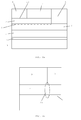
- Figures 1a and 1b illustrate the structure of a Schottky diode device known in the art.
- Figure 2 illustrates the I-V characteristic of the prior art device of figure 1 .
- Figures 3a to 3c show the structure of a Schottky diode according to the invention.
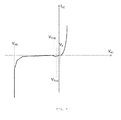
- Figure 4 shows the I-V characteristic of a device according to the invention.
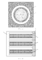
- FIGS 5a and 5b illustrate specific designs of device according to the invention.
- Figure 6 illustrates a device according to the invention, further equipped with a field plate extension.
- Figures 7a to 7g illustrate methods steps in an integrated process for producing a HEMT device and a Schottky diode according to the invention.
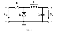
- Figure 8 illustrates a circuit that can be built using the structure produced by the method shown in figures 7a to 7g .
- Figure 1a shows an AlGaN/GaN structure suitable for producing a diode, comprising :
- Figure 1b shows a detail of the Schottky barrier region.
- the device operation is explained on the basis of the I-V characteristic shown in figure 2 .
- the device operates in forward mode. Under these conditions, the diode conducts current, i.e. electrons are free to flow from the anode to the cathode through the channel formed by the 2DEG. Because of the high carrier mobility in the 2DEG, the characteristic approaches the vertical portion of the theoretical IV-characteristic 100 for an ideal device, i.e. high currents can be transported at low voltage drops over the diode.
- Forward conducting mode takes place above the turn-on voltage V F , which depends on the height of the potential barrier of the anode-to-AlGaN Schottky contact 10.
- the threshold voltage V TH is the voltage at which the 2DEG layer becomes depleted in the region underneath the anode. In the case illustrated in figure 2 , V TH ⁇ 0.
- the device is commonly referred to as 'normally ON', i.e. when V AC is zero, the 2DEG is present and current can flow as soon as the voltage is sufficiently high to promote the crossing of the Schottky barrier by the electrons on the channel.
- V TH > 0 When V TH > 0 ('normally OFF' device), the 2DEG is depleted when V AC equals zero, and no current can flow unless V AC exceeds both V TH and the height of the potential barrier of the Schottky junction.
- the turn-on voltage in this case is therefore determined by the higher of these two parameters (V TH and Schottky barrier potential).
- V AC ⁇ 0 Below V TH and in reverse bias mode (V AC ⁇ 0), the normally OFF device will also suffer from a linearly increasing leakage current, as in the case of the normally ON device.
- the device described in US2011/0133251 provides an improvement in terms of the leakage current, but still suffers from a number of drawbacks.
- the anode Laterally with respect to the Schottky contact area in this device, and between said area and the cathode, the anode comprises a portion that is separated from the AlGaN layer by an insulating layer. A further field dielectric region is present between the Schottky contact area and the insulating layer.
- the insulating layer acts to pinch off the 2DEG in a depletion region, when the cathode reaches the pinch voltage of the insulating material. This effectively reduces the leakage current.
- the disadvantage of this structure lies in the large size of the anode which needs to span the width of the distance between the Schottky contact and the insulating layer, said distance including also the field dielectric in between the Schottky contact and the insulating layer.
- This field dielectric therefore increases the resistance in forward bias mode as well as the intrinsic capacitance of the device.
- Figure 3a shows a device according to an embodiment of the invention.
- the same reference numbers 1 through 8 are indicated, referring to the same components as described above for the standard device.
- the shape of the anode 11 is such that the anode comprises a first portion 15 in direct contact with the AlGaN layer 5 and a second portion 16, separated from the AlGaN layer 5 by a thin layer 17 of dielectric material situated between the anode and the cathode.
- the second portion 16 is thus an elongation of the anode, in the direction of the cathode, but separated from the underlying III-nitride layer by the dielectric layer 17.
- Figure 3b shows a detail of the structure of figure 3a , wherein two regions A and B are indicated :
- portions 15 and 16 are directly adjoining, in other words, they are not separated by another region on the surface of the upper III-nitride layer 5.
- This design ensures a minimization of the anode size, as well as of the forward bias mode resistance and the intrinsic capacitance.
- the design ensures the pinching off effect in reverse bias mode in the region underneath the thin dielectric layer 17 so that the leakage current is reduced.
- the thin dielectric layer 17 is formed by a stack of two dielectric layers 27 and 28.
- the lower 27 of said two layers is not only present in the area underneath the elongation portion 16, but covers the surface of the barrier layer 5 up to the cathode 8.
- the upper dielectric layer 28 further has a vertical portion 28' and a horizontal portion 28".
- a passivation layer 7' is present between the first dielectric layer 27 and the upper horizontal portion 28". In this way, the part of layer 27 extending outward from the elongation portion 16, together with the portions 28', 28" and 7' forms the passivation area 7 of the embodiment of figure 3a .
- the lower dielectric layer 27 may be a passivation layer, such as a silicon nitride layer, deposited in-situ after deposition of the barrier layer 5.
- the upper dielectric may be a high K dielectric, such as an aluminium oxide layer. Any embodiment wherein the dielectric layer 17 is a bi-layer of layers 27 and 28 or a multilayer consisting of multiple sublayers is within the scope of the invention, for example layer 28 may continue horizontally towards the cathode 8 (instead of along vertical and upper horizontal portions 28'/28").
- the I-V characteristic in the case of V TH ⁇ 0 ('normally ON' device) of a diode according to the invention is depicted in figure 4 .
- the turn-ON voltage V F coincides with the Schottky contact barrier potential.
- the threshold voltage it is possible to distinguish a threshold voltage V THA ⁇ 0 related to the Schottky contact (region A) and a threshold voltage V THB ⁇ 0 related to the elongation region B.
- the reverse bias region of a diode according to the invention is defined as the range of voltages (between the anode and the cathode), said range being between V BD (reverse breakdown) and the threshold voltage V THA of the region A where the anode is in direct contact with the upper III nitride layer (layer 5 in the figures).
- V BD reverse breakdown
- V THA threshold voltage
- the 2DEG is pinched off by the depletion of the 2DEG in region B, in (i.e. in at least a portion of) the reverse bias region.
- the difference between V THA and V THB is preferably such that the 2DEG is pinched off in a substantial part (e.g. at least 50%) of the reverse bias region.
- Said substantial part is preferably as large as possible, and depends mainly on the thickness and material of the thin dielectric layer 17. According to a preferred embodiment, said substantial part is at least 90% of the reverse bias region, more preferably at least 95%. According to a preferred embodiment, the layer of dielectric material 17 is as thin as possible, meaning :
- Figures 3a-3c show only a schematic representation of a device according to the invention.
- the basic concept is that at each side where the anode is facing the cathode, the anode electrode must be terminated with the over-elongation and the thin dielectric layer 17 underneath.
- the final shape of the device can be circular or multi-fingers, as illustrated in figures 5a and 5b .
- the Numerals 8 and 11 indicate again the cathode and the anode respectively, numeral 16 indicates the location of the elongation portion(s) of the anode structure.
- the thickness of the dielectric layer 17 (or combined thickness of layers 27 and 28) is small compared to the thickness of the passivation layer 7.
- the layer 17 is between 2nm and 30nm thick.
- the elongation portion 16 of the anode is thereby distinguished from a socalled field plate termination of the anode, which is a lateral extension of the anode known in the art.
- Such a field plate is configured to lower the peak of the electric field at the edge of the anode facing the cathode electrode and thereby improve the breakdown of the device.
- Such extensions are applied at a much higher distance from the Schottky barrier contact interface 10.
- the thickness of a dielectric layer between a field plate termination and the Schottky barrier interface is significantly higher than the thickness of the dielectric layer 17 in a device of the invention.
- the field plate therefore cannot replace the elongation portion 16 since a significant pinch-off of the 2DEG cannot take place at voltages V AC that are within the reverse bias region.
- a pinch-off of the 2DEG can only be obtained at negative voltages that are essentially equal to or higher (in absolute value) than the reverse breakdown voltage V BD .
- the anode is additionally equipped with at least one field plate 30 as known in the art.
- a diode according to the invention can be produced by any suitable process, involving the deposition and patterning of layers on a stack of III-nitride layers (e.g. GaN/AlGaN) provided on a base substrate, preferably a silicon substrate.
- III-nitride layers e.g. GaN/AlGaN
- a base substrate preferably a silicon substrate.
- a preferred embodiment is described hereafter, according to which a diode is produced in an integrated process together with a HEMT device.
- the structure of the anode 11 in a diode of the invention is suitable for such integrated processes, given that the dielectric layer or stack of layers 17 can be produced by depositing one or more dielectric layers on a substrate and patterning said layer(s) in one patterning step to form simultaneously the dielectric 17 and the gate dielectric of the HEMT.
- FIG. 7a on a silicon substrate (not shown), a stack of layers is provided by epitaxial growth, similar to the ones shown in figures 1 and 3 , and comprising at least an AlGaN buffer layer 3, GaN channel layer 4 and AlGaN barrier layer 5. These layers may be grown for example by Metal Organic chemical vapour deposition (MOCVD) or Molecular Beam Epitaxy (MBE).
- MOCVD Metal Organic chemical vapour deposition
- MBE Molecular Beam Epitaxy
- a passivation layer 27 is then deposited by in-situ deposition on the AlGaN barrier layer 5, 'in situ' meaning that the passivation layer is deposited in the same process chamber as the layers 3/4/5 and by the same or equivalent process (e.g. MOCVD or MBE).
- Passivation layer 27 is preferably comprising or consisting of silicon nitride (Si 3 Ni 4 hereafter referred to as 'SiN').
- a second passivation layer 36 deposited for example by LPCVD (low pressure chemical vapour deposition) at a temperature higher than 450°C.
- the second passivation layer may also be consisting of or comprising silicon nitride.
- a patterning step (using standard lithography) is performed for patterning the 2 nd passivation layer ( figure 7b ), forming openings 40 and 41 in said layer. This is done by etching said openings, stopping on the surface of the first passivation layer 27. Then a dielectric layer 28 is deposited conformal ( figure 7c ), i.e. following the contours of the topography defined by the openings 40 and 41.
- This can be a layer of Al 2 O 3 of for example 10nm on top of the LPCVD SiN layer 36 and on the sidewalls and bottom of the openings 40 and 41.
- the in-situ deposited passivation layer 27 and the dielectric layer 28 will function together as the gate dielectric of the HEMT device, and at the location of the Schottky diode, these same layers will function as the dielectric 17, as shown in the embodiment of figure 3c .
- the dielectric 28 may be a layer comprising or consisting of Al 2 O 3 , deposited for example by ALD (Atomic Layer Deposition) at a temperature of about 400°C.
- a second patterning step is performed for forming a second opening within the boundaries of the first opening 40.
- the second opening is 43 is formed by etching through the stack of the passivation layer 27 and the dielectric layer 28, stopping on the surface of the barrier layer 5 ( figure 7d ).
- the second opening 43 is located closer to one edge of the first opening 40 than to the opposite edge of said first opening.
- a metal deposition step is performed, filling the openings 43, 40 and 41 with metal 44 and forming a flat metal surface on top of the substrate.
- the metal will serve as the gate metal of the HEMT and the Schottky barrier metal of the diode.
- This metal layer 44 is further patterned ( figure 7f ) to form the gate 50 of a HEMT device and the anode 11 of a Schottky diode according to the invention. Because of the lateral location of the opening 43 inside the larger opening 40, the anode is shaped as in the previously described embodiments : having a Schottky contact portion 15 and an elongation portion 16, with a dielectric layer 17 underneath the elongation portion.
- the dielectric layer 17 here consists of the stack of the in-situ deposited passivation layer 27 and the conformally deposited dielectric layer 28, i.e. the stack of SiN/Al 2 O 3 according to a preferred embodiment.
- the source and drain contacts 52 and 53 of the HEMT device are created ( figure 7g ) by suitable further patterning and deposition steps.
- the source 52 of the HEMT transistor serves as the cathode 8 of the Schottky diode. This structure allows to produce the circuit illustrated in figure 8 , where the HEMT and Schottky diode are indicated as switch S and diode D.
- the above method description discloses also a method for producing a Schottky diode as shown in figure 3c , i.e. without simultaneously producing a HEMT.
- Variations of the embodiment of figure 7 can be envisaged by the skilled person.
- the step of depositing the conformal layer 28 may be regarded as optional (although in that case the layer 27 should preferably be produced in a different material and thickness). If this optional step is not performed, the dielectric 17 of the Schottky diode is formed by the single dielectric layer 27. In the latter embodiment, instead of a single dielectric layer 27, a stack of layers may be deposited.
- the description of a layer being deposited or produced 'on' another layer or substrate includes the options of
Landscapes
- Electrodes Of Semiconductors (AREA)
- Junction Field-Effect Transistors (AREA)
- Insulated Gate Type Field-Effect Transistor (AREA)
Abstract
Description
- The present invention is related to semiconductor devices, in particular to Schottky diode structures produced on a stack of III-nitride material layers, such as an AlGaN/GaN heterostructure.
- Metal-semiconductor diodes, also referred to as Schottky diodes are widely used in rectifying circuits because of their low forward voltage drop and fast switching action. Schottky diodes produced on AlGaN/GaN heterostructures benefit from the high breakdown voltage of the GaN and the high mobility and high electron density of the 2DEG-layer (2-dimensional electron gas) appearing between the GaN and the AlGaN layer as a result of the difference of piezoelectric and spontaneous polarization. There is however the problem of high leakage current when the diode is reverse biased, with high power losses as a consequence. Document
US2011/0133251 discloses a GaN/AlGaN based Schottky diode structure comprising a stack of a GaN layer and an AlGaN layer, with a metal anode on top of the AlGaN layer forming a Schottky contact therewith, and a metal cathode on the AlGaN layer forming an ohmic contact therewith. A field dielectric layer separates the anode and cathode electrically. - The invention aims to provide a structure that does not suffer from the above disadvantages. This aim is achieved by a device and method as disclosed in the appended claims. The invention is thus firstly related to a Schottky diode device comprising
- at least a lower and an upper III-nitride layer forming a heterojunction therebetween, so that a 2DEG layer may be formed in the lower of the two layers,
- a cathode forming an ohmic contact with the upper III-nitride layer,
- an anode comprising a first portion that forms a Schottky barrier contact with the upper III-nitride layer and a second portion that is separated from the upper III-nitride layer by a layer of dielectric material, the second portion being located between the anode and the cathode, the dielectric material being configured to pinch off the 2DEG layer in the reverse bias region of the diode, said first and second portion being directly adjoining,
- a passivation area isolating the anode and cathode from each other.
- In a device according to the invention, said layer of dielectric material separating the second anode portion from the upper III-nitride layer may have a thickness between 2 and 30nm.
- According to an embodiment, the lower III-nitride layer is a GaN layer, and the upper III-nitride layer is an AlGaN layer.
- Said layer of dielectric material may be a stack of dielectric layers. Said layer of dielectric material or at least a first sublayer of said layer of dielectric material may be covering the surface of said upper III-nitride layer between the anode and the cathode.
- According to an embodiment, the device of the invention comprises a passivation layer on and in contact with the upper III-nitride layer, said passivation layer covering the surface of said upper III-nitride layer between the anode and the cathode, wherein said layer of dielectric material consists of a first portion of said passivation layer and of a high-K dielectric layer on and in contact with said first portion of the passivation layer. Said passivation layer may be a layer consisting of or comprising Silicon nitride (Si3N4) and said high K dielectric layer may consist of or comprise Al2O3.
- Said anode may further comprise at least one field plate termination.
- The invention is equally related to a method for producing a Schottky diode according the invention, comprising the steps of :
- Providing or producing a substrate comprising at least a stack of a lower and an upper III-nitride layer forming a heterojunction therebetween,
- Producing a dielectric layer or a stack of dielectric layers on the surface of said upper III-nitride layer,
- Producing a passivation layer on said (stack of) dielectric layer(s),
- Etching a first opening in said passivation layer, stopping on said (stack of) dielectric layer(s),
- Optionally, depositing one or more additional dielectric layers conformally on said passivation layer and in said first opening, so that said one or more additional layers are lining the bottom and sidewalls of said first opening,
- Etching a second opening within the boundaries of said first opening, through said (stack of) dielectric layers and optional additional layers, and stopping on the surface of the upper III-nitride layer, said second opening being located closer to one side of the first opening than to the opposite side of the first opening,
- Filling said first and second openings with a metal,
- Patterning said metal to form the anode of the diode, a portion of said (stack of) dielectric layer(s) and optional additional layers forming said layer of dielectric material between the second portion of the anode and the surface of the upper III-nitride layer,
- Producing the cathode in electrical contact with said heterojunction.
- According to an embodiment of the method of the invention, said step of depositing a dielectric layer or a stack of dielectric layers consists in depositing a first single dielectric layer, the first single dielectric layer is also referred herein as a portion of the passivation layer and wherein the method does comprise a step of conformally depositing a second single dielectric layer on the portion of the passivation layer and in the first opening.
- According to an embodiment, said first single dielectric layer is a layer consisting of or comprising silicon nitride, and the second single dielectric layer is a layer consisting of or comprising Al2O3.
- The steps of the method of the invention may be integrated with the steps of forming a HEMT device on said substrate, wherein a portion of said dielectric layer or said stack of dielectric layers, optionally further comprising one or more additional dielectric layers is used as the gate dielectric of the HEMT device, and wherein a portion of said metal layer is used as the gate metal of the HEMT device.
- The invention is equally related to a semiconductor device comprising a Schottky diode according to the invention and a HEMT device, wherein :
- the layer of dielectric material between the second portion of the anode and the upper III-nitride layer and
- the gate dielectric of the HEMT
are mutually identical in terms of their thickness and composition. According to different embodiments, both the layer of dielectric material between the second portion of the anode and the upper III-nitride layer, and the gate dielectric of the HEMT consist of a first single dielectric layer and a second single dielectric layer on and in contact with said first single dielectric layer. Said first single dielectric layer consists of or comprises Silicon nitride (Si3N4) and said second dielectric layer consists of or comprises a high-K material, in particular Al2O3. -
Figures 1a and 1b illustrate the structure of a Schottky diode device known in the art. -
Figure 2 illustrates the I-V characteristic of the prior art device offigure 1 . -
Figures 3a to 3c show the structure of a Schottky diode according to the invention. -
Figure 4 shows the I-V characteristic of a device according to the invention. -
Figures 5a and 5b illustrate specific designs of device according to the invention. -
Figure 6 illustrates a device according to the invention, further equipped with a field plate extension. -
Figures 7a to 7g illustrate methods steps in an integrated process for producing a HEMT device and a Schottky diode according to the invention. -
Figure 8 illustrates a circuit that can be built using the structure produced by the method shown infigures 7a to 7g . - As a point of reference, the operation of a standard Schottky barrier diode is summarized hereafter, based on
figures 1a and 1b. Figure 1a shows an AlGaN/GaN structure suitable for producing a diode, comprising : - Substrate 1 : this is the carrier where the epitaxial layers are grown. It can be a silicon or a silicon carbide substrate for example.
- Nucleation layer 2 : to mitigate the mismatch between the
substrate 1 and thebuffer layer 3. -
Buffer layer 3. Preferably this layer is constituted by several Al1-xGaxN layers with different aluminium content (x). It improves the buffer breakdown of the device, minimizes the mismatch between thesubstrate 1 and theGaN layer 4, and improves the confinement of the 2DEG at the AlGaN/GaN interface. - GaN channel layer 4 : this is realized by the deposition of non-doped GaN. In this layer the channel for the conduction of the device is formed.
- AlGaN
barrier Layer 5. - 2DEG 6 (two dimensional electron gas) : this layer is the consequence of the growth of the
AlGaN barrier layer 5 on top of theGaN channel layer 4. It is a gas of electrons with high density confined at the AlGaN/GaN interface. The carriers flow through this channel when the device is conducting current. - Passivation area 7 : this may be one or a stack of dielectric layers deposited on the surface of the device. It improves the interface with the layers on top of it and prevents the action of impurities and external ambient factors to damage the device.
- Cathode 8: this is preferably a stack of different metals selected in order to form a low-resistive ohmic contact with the
AlGaN barrier 5. - Anode 9 : this is a metal electrode that forms a
Schottky contact 10 with theAlGaN layer 5. -
Figure 1b shows a detail of the Schottky barrier region. The device operation is explained on the basis of the I-V characteristic shown infigure 2 . At a sufficiently high positive voltage, region 20, the device operates in forward mode. Under these conditions, the diode conducts current, i.e. electrons are free to flow from the anode to the cathode through the channel formed by the 2DEG. Because of the high carrier mobility in the 2DEG, the characteristic approaches the vertical portion of the theoretical IV-characteristic 100 for an ideal device, i.e. high currents can be transported at low voltage drops over the diode. Forward conducting mode takes place above the turn-on voltage VF, which depends on the height of the potential barrier of the anode-to-AlGaN Schottky contact 10. - The threshold voltage VTH is the voltage at which the 2DEG layer becomes depleted in the region underneath the anode. In the case illustrated in
figure 2 , VTH < 0. When this is the case, the device is commonly referred to as 'normally ON', i.e. when VAC is zero, the 2DEG is present and current can flow as soon as the voltage is sufficiently high to promote the crossing of the Schottky barrier by the electrons on the channel. - In reverse bias mode, i.e. for voltages lower than 0, the ideal characteristic 100 should also be approached as closely as possible. In the actual device, a leakage current appears however, as the negative voltage increases (in absolute value) : in a
first region 21 of the characteristic, the 2DEG underneath the Schottky contact area is not fully depleted, and a small leakage current appears, even when the Schottky barrier is fully in reverse bias, mainly caused by electrons that are crossing the barrier due to tunnelling effects for example. At the threshold voltage VTH, the 2DEG is fully depleted, but at the edge of the Schottky region, inarea 25 indicated infigure 1b , electrons are still leaking through to the anode. As the negative voltage VAC increases in absolute value, this leakage current increases linearly (region 22 infigure 2 ), with power losses as a consequence. At voltage VBD, the device ultimately goes into reverse breakdown. - When VTH > 0 ('normally OFF' device), the 2DEG is depleted when VAC equals zero, and no current can flow unless VAC exceeds both VTH and the height of the potential barrier of the Schottky junction. The turn-on voltage in this case is therefore determined by the higher of these two parameters (VTH and Schottky barrier potential). Below VTH and in reverse bias mode (VAC < 0), the normally OFF device will also suffer from a linearly increasing leakage current, as in the case of the normally ON device.
- The device described in
US2011/0133251 provides an improvement in terms of the leakage current, but still suffers from a number of drawbacks. Laterally with respect to the Schottky contact area in this device, and between said area and the cathode, the anode comprises a portion that is separated from the AlGaN layer by an insulating layer. A further field dielectric region is present between the Schottky contact area and the insulating layer. When the device goes into reverse breakdown mode, the insulating layer acts to pinch off the 2DEG in a depletion region, when the cathode reaches the pinch voltage of the insulating material. This effectively reduces the leakage current. The disadvantage of this structure lies in the large size of the anode which needs to span the width of the distance between the Schottky contact and the insulating layer, said distance including also the field dielectric in between the Schottky contact and the insulating layer. The presence of this field dielectric therefore increases the resistance in forward bias mode as well as the intrinsic capacitance of the device. -
Figure 3a shows a device according to an embodiment of the invention. Thesame reference numbers 1 through 8 are indicated, referring to the same components as described above for the standard device. Characteristically for the invention, the shape of theanode 11 is such that the anode comprises afirst portion 15 in direct contact with theAlGaN layer 5 and asecond portion 16, separated from theAlGaN layer 5 by athin layer 17 of dielectric material situated between the anode and the cathode. Thesecond portion 16 is thus an elongation of the anode, in the direction of the cathode, but separated from the underlying III-nitride layer by thedielectric layer 17.Figure 3b shows a detail of the structure offigure 3a , wherein two regions A and B are indicated : - Region A is the contact region between the anode's
first portion 15 and theAlGaN barrier layer 5. Through this area the current flows from the anode to the cathode when the Schottky diode is in forward bias mode. The surface area of this contact is one of the factors that determine the total amount of current passing into the device. - Region B is the contact region between the
dielectric layer 17 and theAlGaN layer 5. It is the region situated underneath theelongation portion 16 of the anode extending over the anode-to-cathode region. Thisportion 16 of the anode is not in contact with theAlGaN barrier layer 5, but separated from it by thethin dielectric layer 17. - In the structure of the invention,
portions 15 and 16 (and thus also regions A and B) are directly adjoining, in other words, they are not separated by another region on the surface of the upper III-nitride layer 5. This design ensures a minimization of the anode size, as well as of the forward bias mode resistance and the intrinsic capacitance. At the same time, the design ensures the pinching off effect in reverse bias mode in the region underneath thethin dielectric layer 17 so that the leakage current is reduced. - A specific embodiment of a diode structure according to the invention is shown in
figure 3c . According to this embodiment, thethin dielectric layer 17 is formed by a stack of twodielectric layers elongation portion 16, but covers the surface of thebarrier layer 5 up to thecathode 8. Theupper dielectric layer 28 further has a vertical portion 28' and ahorizontal portion 28". A passivation layer 7' is present between thefirst dielectric layer 27 and the upperhorizontal portion 28". In this way, the part oflayer 27 extending outward from theelongation portion 16, together with theportions 28', 28" and 7' forms thepassivation area 7 of the embodiment offigure 3a . This particular embodiment (figure 3c ) is useful in that it allows an easy integration with the fabrication of a HEMT transistor, as illustrated further in this description. The lowerdielectric layer 27 may be a passivation layer, such as a silicon nitride layer, deposited in-situ after deposition of thebarrier layer 5. The upper dielectric may be a high K dielectric, such as an aluminium oxide layer. Any embodiment wherein thedielectric layer 17 is a bi-layer oflayers example layer 28 may continue horizontally towards the cathode 8 (instead of along vertical and upper horizontal portions 28'/28"). - The I-V characteristic in the case of VTH < 0 ('normally ON' device) of a diode according to the invention is depicted in
figure 4 . As in the prior art device, the turn-ON voltage VF coincides with the Schottky contact barrier potential. Referring to the threshold voltage it is possible to distinguish a threshold voltage VTHA < 0 related to the Schottky contact (region A) and a threshold voltage VTHB < 0 related to the elongation region B. When the voltage across the device is negative (reverse blocking mode) but not sufficiently negative to be below one of the two threshold voltages, the channel is not fully depleted, carriers from the 2DEG can be attracted to the anode, thus the leakage current of the device is established by the Schottky barrier height in reverse polarization. When VAC is lower than VTHB the channel area below region B is fully depleted, i.e. the channel area is pinched off. This ensures that substantially no leakage current appears, as the distance betweenedge area 26 and the anode is increased by the presence of theelongation 16. In this working region the leakage current is minimized by the effect of the anode elongation. In case of VTHB < VTHA < 0 a small leakage current may still appear when VTHB < VAC < VTHA. The real effect of blocking the gate leakage will appear only when VAC < VTHB. - The reverse bias region of a diode according to the invention is defined as the range of voltages (between the anode and the cathode), said range being between VBD (reverse breakdown) and the threshold voltage VTHA of the region A where the anode is in direct contact with the upper III nitride layer (
layer 5 in the figures). In a diode of the invention, the 2DEG is pinched off by the depletion of the 2DEG in region B, in (i.e. in at least a portion of) the reverse bias region. The difference between VTHA and VTHB is preferably such that the 2DEG is pinched off in a substantial part (e.g. at least 50%) of the reverse bias region. Said substantial part is preferably as large as possible, and depends mainly on the thickness and material of thethin dielectric layer 17. According to a preferred embodiment, said substantial part is at least 90% of the reverse bias region, more preferably at least 95%. According to a preferred embodiment, the layer ofdielectric material 17 is as thin as possible, meaning : - it must be thick enough to ensure a complete separation of the anode and the upper III-nitride layer, so that no Schottky contact is present in region B (i.e. the region between the
elongation portion 16 of the anode and the upper III-nitride layer 5), - it must be thin enough so that the threshold voltage VTHB is as close as possible to the threshold voltage VTHA of the Schottky contact in region A.
-
Figures 3a-3c show only a schematic representation of a device according to the invention. The basic concept is that at each side where the anode is facing the cathode, the anode electrode must be terminated with the over-elongation and thethin dielectric layer 17 underneath. The final shape of the device can be circular or multi-fingers, as illustrated infigures 5a and 5b . TheNumerals - The thickness of the dielectric layer 17 (or combined thickness of
layers 27 and 28) is small compared to the thickness of thepassivation layer 7. Preferably, thelayer 17 is between 2nm and 30nm thick. Theelongation portion 16 of the anode is thereby distinguished from a socalled field plate termination of the anode, which is a lateral extension of the anode known in the art. Such a field plate is configured to lower the peak of the electric field at the edge of the anode facing the cathode electrode and thereby improve the breakdown of the device. Such extensions are applied at a much higher distance from the Schottkybarrier contact interface 10. In other words, the thickness of a dielectric layer between a field plate termination and the Schottky barrier interface is significantly higher than the thickness of thedielectric layer 17 in a device of the invention. The field plate therefore cannot replace theelongation portion 16 since a significant pinch-off of the 2DEG cannot take place at voltages VAC that are within the reverse bias region. In other words, a pinch-off of the 2DEG can only be obtained at negative voltages that are essentially equal to or higher (in absolute value) than the reverse breakdown voltage VBD. According to an embodiment of the invention, illustrated infigure 6 , the anode is additionally equipped with at least onefield plate 30 as known in the art. - A diode according to the invention can be produced by any suitable process, involving the deposition and patterning of layers on a stack of III-nitride layers (e.g. GaN/AlGaN) provided on a base substrate, preferably a silicon substrate. A preferred embodiment is described hereafter, according to which a diode is produced in an integrated process together with a HEMT device. The structure of the
anode 11 in a diode of the invention is suitable for such integrated processes, given that the dielectric layer or stack oflayers 17 can be produced by depositing one or more dielectric layers on a substrate and patterning said layer(s) in one patterning step to form simultaneously the dielectric 17 and the gate dielectric of the HEMT. - The steps of such an integrated process for forming a semiconductor device comprising a diode according to the invention and a HEMT transistor, are illustrated in
figures 7a to 7g . As seen infigure 7a : on a silicon substrate (not shown), a stack of layers is provided by epitaxial growth, similar to the ones shown infigures 1 and3 , and comprising at least anAlGaN buffer layer 3,GaN channel layer 4 andAlGaN barrier layer 5. These layers may be grown for example by Metal Organic chemical vapour deposition (MOCVD) or Molecular Beam Epitaxy (MBE). Apassivation layer 27 is then deposited by in-situ deposition on theAlGaN barrier layer 5, 'in situ' meaning that the passivation layer is deposited in the same process chamber as thelayers 3/4/5 and by the same or equivalent process (e.g. MOCVD or MBE).Passivation layer 27 is preferably comprising or consisting of silicon nitride (Si3Ni4 hereafter referred to as 'SiN'). This is followed by the deposition of asecond passivation layer 36, deposited for example by LPCVD (low pressure chemical vapour deposition) at a temperature higher than 450°C. The second passivation layer may also be consisting of or comprising silicon nitride. - A patterning step (using standard lithography) is performed for patterning the 2nd passivation layer (
figure 7b ), formingopenings first passivation layer 27. Then adielectric layer 28 is deposited conformal (figure 7c ), i.e. following the contours of the topography defined by theopenings LPCVD SiN layer 36 and on the sidewalls and bottom of theopenings passivation layer 27 and thedielectric layer 28 will function together as the gate dielectric of the HEMT device, and at the location of the Schottky diode, these same layers will function as the dielectric 17, as shown in the embodiment offigure 3c . The dielectric 28 may be a layer comprising or consisting of Al2O3, deposited for example by ALD (Atomic Layer Deposition) at a temperature of about 400°C. - A second patterning step is performed for forming a second opening within the boundaries of the
first opening 40. The second opening is 43 is formed by etching through the stack of thepassivation layer 27 and thedielectric layer 28, stopping on the surface of the barrier layer 5 (figure 7d ). Thesecond opening 43 is located closer to one edge of thefirst opening 40 than to the opposite edge of said first opening. Then (figure 7e ) a metal deposition step is performed, filling theopenings metal 44 and forming a flat metal surface on top of the substrate. The metal will serve as the gate metal of the HEMT and the Schottky barrier metal of the diode. Thismetal layer 44 is further patterned (figure 7f ) to form thegate 50 of a HEMT device and theanode 11 of a Schottky diode according to the invention. Because of the lateral location of theopening 43 inside thelarger opening 40, the anode is shaped as in the previously described embodiments : having aSchottky contact portion 15 and anelongation portion 16, with adielectric layer 17 underneath the elongation portion. Thedielectric layer 17 here consists of the stack of the in-situ depositedpassivation layer 27 and the conformally depositeddielectric layer 28, i.e. the stack of SiN/Al2O3 according to a preferred embodiment. Then the source anddrain contacts figure 7g ) by suitable further patterning and deposition steps. Thesource 52 of the HEMT transistor serves as thecathode 8 of the Schottky diode. This structure allows to produce the circuit illustrated infigure 8 , where the HEMT and Schottky diode are indicated as switch S and diode D. - When leaving out all references to a HEMT device, the above method description discloses also a method for producing a Schottky diode as shown in
figure 3c , i.e. without simultaneously producing a HEMT. Variations of the embodiment offigure 7 can be envisaged by the skilled person. For example, the step of depositing theconformal layer 28 may be regarded as optional (although in that case thelayer 27 should preferably be produced in a different material and thickness). If this optional step is not performed, the dielectric 17 of the Schottky diode is formed by thesingle dielectric layer 27. In the latter embodiment, instead of asingle dielectric layer 27, a stack of layers may be deposited. - While the invention has been illustrated and described in detail in the drawings and foregoing description, such illustration and description are to be considered illustrative or exemplary and not restrictive. Other variations to the disclosed embodiments can be understood and effected by those skilled in the art in practicing the claimed invention, from a study of the drawings, the disclosure and the appended claims. In the claims, the word "comprising" does not exclude other elements or steps, and the indefinite article "a" or "an" does not exclude a plurality. The mere fact that certain measures are recited in mutually different dependent claims does not indicate that a combination of these measures cannot be used to advantage. Any reference signs in the claims should not be construed as limiting the scope.
- The foregoing description details certain embodiments of the invention. It will be appreciated, however, that no matter how detailed the foregoing appears in text, the invention may be practiced in many ways, and is therefore not limited to the embodiments disclosed. It should be noted that the use of particular terminology when describing certain features or aspects of the invention should not be taken to imply that the terminology is being re-defined herein to be restricted to include any specific characteristics of the features or aspects of the invention with which that terminology is associated.
- Unless specifically specified, the description of a layer being deposited or produced 'on' another layer or substrate, includes the options of
- said layer being produced or deposited directly on, i.e. in contact with, said other layer or substrate, and
Claims (15)
- A Schottky diode device comprising :• at least a lower and an upper III-nitride layer (4,5) forming a heterojunction therebetween, so that a 2DEG layer may be formed in the lower of the two layers,• a cathode (8) forming an ohmic contact with the upper III-nitride layer,• an anode (11) comprising a first portion (15) that forms a Schottky barrier contact (10) with the upper III-nitride layer and a second portion (16) that is separated from the upper III-nitride layer by a layer of dielectric material (17), the second portion being located between the anode and the cathode, the dielectric material being configured to pinch off the 2DEG layer in the reverse bias region of the diode, said first and second portion being directly adjoining,• a passivation area (7) isolating the anode and cathode from each other.
- Device according to claim 1, wherein said layer of dielectric material (17) separating the second anode portion from the upper III-nitride layer has a thickness between 2 and 30nm.
- Device according to claim 1 or 2, wherein the lower III-nitride layer (4) is a GaN layer, and the upper III-nitride layer (5) is an AlGaN layer.
- Device according to any one of claims 1 to 3, wherein said layer of dielectric material (17) is a stack of dielectric layers.
- Device according to any one of claims 1 to 4, wherein said layer (17) of dielectric material or at least a first sublayer of said layer (17) of dielectric material is covering the surface of said upper III-nitride layer (5) between the anode (11) and the cathode (8).
- Device according to claim 5, comprising a passivation layer on and in contact with the upper III-nitride layer (5), said passivation layer covering the surface of said upper III-nitride layer between the anode and the cathode, wherein said layer (17) of dielectric material consists of a first portion (27) of said passivation layer and a high-K dielectric layer (28) on and in contact with said first portion of the passivation layer.
- Device according to claim 6, wherein said passivation layer is a layer consisting of or comprising Silicon nitride (Si3N4) and wherein said high K dielectric layer consists of or comprises Al2O3.
- Device according to any one of the previous claims, wherein said anode further comprises at least one field plate termination (30).
- Method for producing a Schottky diode according to any one of claims 1 to 8, comprising the steps of :• Providing or producing a substrate (1) comprising at least a stack of a lower and an upper III-nitride layer (4,5) forming a heterojunction therebetween,• Producing a dielectric layer (27) or a stack of dielectric layers on the surface of said upper III-nitride layer (5),• Producing a passivation layer (36) on said (stack of) dielectric layer(s) (27),• Etching a first opening (40) in said passivation layer (36), stopping on said (stack of) dielectric layer(s) (27),• Optionally, depositing one or more additional dielectric layers (28) conformally on said passivation layer (36) and in said first opening (40), so that said one or more additional layers (28) are lining the bottom and sidewalls of said first opening (40),• Etching a second opening (43) within the boundaries of said first opening (40), through said (stack of) dielectric layers (27) and optional additional layers (28), and stopping on the surface of the upper III-nitride layer (5), said second opening being located closer to one side of the first opening (40) than to the opposite side of the first opening (40),• Filling said first and second openings (40,43) with a metal (44),• Patterning said metal to form the anode (11) of the diode, a portion of said (stack of) dielectric layer(s) (27) and optional additional layers (28) forming said layer (17) of dielectric material between the second portion (16) of the anode and the surface of the upper III-nitride layer (5),• Producing the cathode (8,52) in electrical contact with said heterojunction.
- Method according to claim 9, wherein said step of depositing a dielectric layer (27) or a stack of dielectric layers consists in depositing a first single dielectric layer (27), and wherein the method does comprise a step of conformally depositing a second single dielectric layer on the passivation layer (36) and in the first opening (40).
- Method according to claim 10, wherein said first single dielectric layer is a layer consisting of or comprising silicon nitride, and the second single dielectric layer (28) is a layer consisting of or comprising Al2O3.
- Method according to any one of claims 9 to 11, wherein said steps are integrated with the steps of forming a HEMT device on said substrate, wherein a portion of said dielectric layer (27) or said stack of dielectric layers, optionally further comprising one or more additional dielectric layers (28) is used as the gate dielectric of the HEMT device, and wherein a portion of said metal layer (44) is used as the gate metal of the HEMT device.
- A semiconductor device comprising a Schottky diode according to any one of claims 1 to 8 and a HEMT device, wherein :• the layer (17) of dielectric material between the second portion (16) of the anode (11) and the upper III-nitride layer (5) and• the gate dielectric of the HEMTare mutually identical in terms of their thickness and composition.
- The semiconductor device of claim 13, wherein said layer (17) of dielectric material consists of a first single dielectric layer (27) and a second single dielectric layer (28) on and in contact with said first single dielectric layer.
- The semiconductor device of claim 14, wherein said first single dielectric layer consists of or comprises Silicon nitride (Si3N4) and wherein said second dielectric layer consists of or comprises Al2O3.
Priority Applications (3)
| Application Number | Priority Date | Filing Date | Title |
|---|---|---|---|
| EP12188867.1A EP2722890B1 (en) | 2012-10-17 | 2012-10-17 | Schottky diode structure and method of fabrication |
| JP2013189228A JP6182029B2 (en) | 2012-10-17 | 2013-09-12 | Schottky diode structure and manufacturing method thereof |
| US14/056,643 US9711601B2 (en) | 2012-10-17 | 2013-10-17 | Schottky diode structure and method of fabrication |
Applications Claiming Priority (1)
| Application Number | Priority Date | Filing Date | Title |
|---|---|---|---|
| EP12188867.1A EP2722890B1 (en) | 2012-10-17 | 2012-10-17 | Schottky diode structure and method of fabrication |
Publications (2)
| Publication Number | Publication Date |
|---|---|
| EP2722890A1 true EP2722890A1 (en) | 2014-04-23 |
| EP2722890B1 EP2722890B1 (en) | 2020-12-16 |
Family
ID=47115404
Family Applications (1)
| Application Number | Title | Priority Date | Filing Date |
|---|---|---|---|
| EP12188867.1A Active EP2722890B1 (en) | 2012-10-17 | 2012-10-17 | Schottky diode structure and method of fabrication |
Country Status (3)
| Country | Link |
|---|---|
| US (1) | US9711601B2 (en) |
| EP (1) | EP2722890B1 (en) |
| JP (1) | JP6182029B2 (en) |
Cited By (1)
| Publication number | Priority date | Publication date | Assignee | Title |
|---|---|---|---|---|
| CN106449772A (en) * | 2015-08-04 | 2017-02-22 | 电力集成公司 | Method for manufacturing lateral Schottky diode and diode |
Families Citing this family (23)
| Publication number | Priority date | Publication date | Assignee | Title |
|---|---|---|---|---|
| US20150187618A1 (en) * | 2013-12-30 | 2015-07-02 | Enkris Semiconductor, Inc. | System and method for forming gan-based device |
| JP6345126B2 (en) * | 2015-01-21 | 2018-06-20 | 三菱電機株式会社 | Schottky barrier diode |
| CN105355555A (en) * | 2015-10-28 | 2016-02-24 | 中国科学院微电子研究所 | GaN-based enhanced power electronic device and preparation method thereof |
| CN107104040A (en) * | 2016-02-23 | 2017-08-29 | 北京大学 | The anode fabrication method of gallium nitride Schottky diode |
| CN107230630A (en) * | 2016-03-25 | 2017-10-03 | 北京大学 | The preparation method of gallium nitride field effect transistor |
| US10651317B2 (en) * | 2016-04-15 | 2020-05-12 | Macom Technology Solutions Holdings, Inc. | High-voltage lateral GaN-on-silicon Schottky diode |
| US20170301780A1 (en) | 2016-04-15 | 2017-10-19 | Macom Technology Solutions Holdings, Inc. | High-voltage gan high electron mobility transistors with reduced leakage current |
| KR102430498B1 (en) | 2016-06-28 | 2022-08-09 | 삼성전자주식회사 | Elecronic Device Having a Schottky Diode |
| CN106571387A (en) * | 2016-10-14 | 2017-04-19 | 西安电子科技大学 | High K material-based stacked-gate AlGaN/GaN high-electron mobility MOS device |
| US10204778B2 (en) * | 2016-12-28 | 2019-02-12 | QROMIS, Inc. | Method and system for vertical power devices |
| WO2018236406A1 (en) * | 2017-06-24 | 2018-12-27 | Intel Corporation | Group iii-nitride heterostructure diodes |
| US11545586B2 (en) | 2017-09-29 | 2023-01-03 | Intel Corporation | Group III-nitride Schottky diode |
| DE112017007912T5 (en) | 2017-09-29 | 2020-07-02 | Intel Corporation | GROUP III NITRIDE ANTENNA DIODE |
| US10950598B2 (en) | 2018-01-19 | 2021-03-16 | Macom Technology Solutions Holdings, Inc. | Heterolithic microwave integrated circuits including gallium-nitride devices formed on highly doped semiconductor |
| US11233047B2 (en) | 2018-01-19 | 2022-01-25 | Macom Technology Solutions Holdings, Inc. | Heterolithic microwave integrated circuits including gallium-nitride devices on highly doped regions of intrinsic silicon |
| US11056483B2 (en) | 2018-01-19 | 2021-07-06 | Macom Technology Solutions Holdings, Inc. | Heterolithic microwave integrated circuits including gallium-nitride devices on intrinsic semiconductor |
| US11081555B2 (en) * | 2018-06-27 | 2021-08-03 | Ohio State Innovation Foundation | Electronic devices with ultra-high dielectric constant passivation and high mobility materials |
| CN111816701B (en) * | 2019-04-12 | 2024-12-27 | 广东致能科技有限公司 | Semiconductor device and method for manufacturing the same |
| CN112420850B (en) * | 2019-08-23 | 2024-04-12 | 苏州捷芯威半导体有限公司 | Semiconductor device and preparation method thereof |
| US11600614B2 (en) | 2020-03-26 | 2023-03-07 | Macom Technology Solutions Holdings, Inc. | Microwave integrated circuits including gallium-nitride devices on silicon |
| CN114530492A (en) * | 2022-03-18 | 2022-05-24 | 成都智达和创信息科技有限公司 | Lateral gallium nitride schottky diode structure with hybrid high-k dielectric field plate |
| CN115588689B (en) * | 2022-10-27 | 2026-06-16 | 天狼芯半导体(成都)有限公司 | Gallium nitride Schottky diode and its fabrication method |
| CN118073427A (en) * | 2024-02-19 | 2024-05-24 | 松山湖材料实验室 | Semiconductor device and method for manufacturing the same |
Citations (3)
| Publication number | Priority date | Publication date | Assignee | Title |
|---|---|---|---|---|
| US20080283870A1 (en) * | 2007-05-18 | 2008-11-20 | Sanken Electric Co., Ltd. | Field-effect semiconductor device |
| US20100019279A1 (en) * | 2008-04-02 | 2010-01-28 | The Hong Kong University Of Science And Technology | Integrated HEMT and Lateral Field-Effect Rectifier Combinations, Methods, and Systems |
| US20110133251A1 (en) | 2009-12-07 | 2011-06-09 | International Rectifier Corporation | Gated algan/gan heterojunction schottky device |
Family Cites Families (5)
| Publication number | Priority date | Publication date | Assignee | Title |
|---|---|---|---|---|
| US7875950B2 (en) * | 2007-03-08 | 2011-01-25 | Semiconductor Components Industries, Llc | Schottky diode structure with multi-portioned guard ring and method of manufacture |
| JP2010087274A (en) * | 2008-09-30 | 2010-04-15 | Sanken Electric Co Ltd | Semiconductor device |
| US7842974B2 (en) * | 2009-02-18 | 2010-11-30 | Alpha & Omega Semiconductor, Inc. | Gallium nitride heterojunction schottky diode |
| US8390000B2 (en) * | 2009-08-28 | 2013-03-05 | Transphorm Inc. | Semiconductor devices with field plates |
| US8716141B2 (en) * | 2011-03-04 | 2014-05-06 | Transphorm Inc. | Electrode configurations for semiconductor devices |
-
2012
- 2012-10-17 EP EP12188867.1A patent/EP2722890B1/en active Active
-
2013
- 2013-09-12 JP JP2013189228A patent/JP6182029B2/en active Active
- 2013-10-17 US US14/056,643 patent/US9711601B2/en active Active
Patent Citations (3)
| Publication number | Priority date | Publication date | Assignee | Title |
|---|---|---|---|---|
| US20080283870A1 (en) * | 2007-05-18 | 2008-11-20 | Sanken Electric Co., Ltd. | Field-effect semiconductor device |
| US20100019279A1 (en) * | 2008-04-02 | 2010-01-28 | The Hong Kong University Of Science And Technology | Integrated HEMT and Lateral Field-Effect Rectifier Combinations, Methods, and Systems |
| US20110133251A1 (en) | 2009-12-07 | 2011-06-09 | International Rectifier Corporation | Gated algan/gan heterojunction schottky device |
Non-Patent Citations (1)
| Title |
|---|
| SEUNG-CHUL LEE ET AL.: "Suppression of leakage current of Ni/Au Schorrky barrier diode fabricated on AlGaN/GaN heterostructure by oxidation", JAPANESE JOURNAL OF APPLIED PHYSICS, vol. 45, no. 4B, 2006, Japan, pages 3398 - 3400, XP002693514 * |
Cited By (1)
| Publication number | Priority date | Publication date | Assignee | Title |
|---|---|---|---|---|
| CN106449772A (en) * | 2015-08-04 | 2017-02-22 | 电力集成公司 | Method for manufacturing lateral Schottky diode and diode |
Also Published As
| Publication number | Publication date |
|---|---|
| US9711601B2 (en) | 2017-07-18 |
| JP6182029B2 (en) | 2017-08-16 |
| US20140103357A1 (en) | 2014-04-17 |
| JP2014090159A (en) | 2014-05-15 |
| EP2722890B1 (en) | 2020-12-16 |
Similar Documents
| Publication | Publication Date | Title |
|---|---|---|
| EP2722890B1 (en) | Schottky diode structure and method of fabrication | |
| EP2793255B1 (en) | Manufacturing method of a semiconductor device comprising a schottky diode and a high electron mobility transistor | |
| US9520491B2 (en) | Electrodes for semiconductor devices and methods of forming the same | |
| US9461122B2 (en) | Semiconductor device and manufacturing method for the same | |
| US8890212B2 (en) | Normally-off high electron mobility transistor | |
| EP2168162B1 (en) | Hetero-structure field effect transistor, integrated circuit including a hetero-structure field effect transistor and method for manufacturing a hetero-structure field effect transistor | |
| US8962461B2 (en) | GaN HEMTs and GaN diodes | |
| US9666705B2 (en) | Contact structures for compound semiconductor devices | |
| US20120223320A1 (en) | Electrode configurations for semiconductor devices | |
| CN108807527A (en) | IIIA Nitride HEMT with Tunnel Diode in Gate Stack | |
| CN110476254B (en) | Heterojunction transistor with vertical structure | |
| CN114270532B (en) | Semiconductor device and manufacturing method thereof | |
| JP5549081B2 (en) | Semiconductor device and manufacturing method thereof | |
| US8558242B2 (en) | Vertical GaN-based metal insulator semiconductor FET | |
| US9269793B2 (en) | Method and system for a gallium nitride self-aligned vertical MESFET | |
| JP5100002B2 (en) | Nitride semiconductor device | |
| WO2024092419A1 (en) | Nitride-based semiconductor device and method for manufacturing the same | |
| KR102029834B1 (en) | Power semiconducror device | |
| EP4723168A1 (en) | Semiconductor device | |
| KR102113253B1 (en) | Nitride based Semiconductor Device |
Legal Events
| Date | Code | Title | Description |
|---|---|---|---|
| PUAI | Public reference made under article 153(3) epc to a published international application that has entered the european phase |
Free format text: ORIGINAL CODE: 0009012 |
|
| AK | Designated contracting states |
Kind code of ref document: A1 Designated state(s): AL AT BE BG CH CY CZ DE DK EE ES FI FR GB GR HR HU IE IS IT LI LT LU LV MC MK MT NL NO PL PT RO RS SE SI SK SM TR |
|
| AX | Request for extension of the european patent |
Extension state: BA ME |
|
| 17P | Request for examination filed |
Effective date: 20141015 |
|
| RBV | Designated contracting states (corrected) |
Designated state(s): AL AT BE BG CH CY CZ DE DK EE ES FI FR GB GR HR HU IE IS IT LI LT LU LV MC MK MT NL NO PL PT RO RS SE SI SK SM TR |
|
| STAA | Information on the status of an ep patent application or granted ep patent |
Free format text: STATUS: EXAMINATION IS IN PROGRESS |
|
| 17Q | First examination report despatched |
Effective date: 20161220 |
|
| RAP1 | Party data changed (applicant data changed or rights of an application transferred) |
Owner name: IMEC VZW |
|
| REG | Reference to a national code |
Ref country code: DE Ref legal event code: R079 Ref document number: 602012073721 Country of ref document: DE Free format text: PREVIOUS MAIN CLASS: H01L0029200000 Ipc: H01L0029872000 |
|
| RIC1 | Information provided on ipc code assigned before grant |
Ipc: H01L 21/328 20060101ALI20200615BHEP Ipc: H01L 29/778 20060101ALI20200615BHEP Ipc: H01L 29/20 20060101ALN20200615BHEP Ipc: H01L 29/40 20060101ALN20200615BHEP Ipc: H01L 27/06 20060101ALI20200615BHEP Ipc: H01L 29/872 20060101AFI20200615BHEP Ipc: H01L 21/8252 20060101ALI20200615BHEP |
|
| RIC1 | Information provided on ipc code assigned before grant |
Ipc: H01L 29/40 20060101ALN20200622BHEP Ipc: H01L 29/872 20060101AFI20200622BHEP Ipc: H01L 27/06 20060101ALI20200622BHEP Ipc: H01L 29/20 20060101ALN20200622BHEP Ipc: H01L 21/328 20060101ALI20200622BHEP Ipc: H01L 21/8252 20060101ALI20200622BHEP Ipc: H01L 29/778 20060101ALI20200622BHEP |
|
| GRAP | Despatch of communication of intention to grant a patent |
Free format text: ORIGINAL CODE: EPIDOSNIGR1 |
|
| STAA | Information on the status of an ep patent application or granted ep patent |
Free format text: STATUS: GRANT OF PATENT IS INTENDED |
|
| INTG | Intention to grant announced |
Effective date: 20200921 |
|
| GRAS | Grant fee paid |
Free format text: ORIGINAL CODE: EPIDOSNIGR3 |
|
| GRAA | (expected) grant |
Free format text: ORIGINAL CODE: 0009210 |
|
| STAA | Information on the status of an ep patent application or granted ep patent |
Free format text: STATUS: THE PATENT HAS BEEN GRANTED |
|
| AK | Designated contracting states |
Kind code of ref document: B1 Designated state(s): AL AT BE BG CH CY CZ DE DK EE ES FI FR GB GR HR HU IE IS IT LI LT LU LV MC MK MT NL NO PL PT RO RS SE SI SK SM TR |
|
| REG | Reference to a national code |
Ref country code: GB Ref legal event code: FG4D |
|
| REG | Reference to a national code |
Ref country code: IE Ref legal event code: FG4D |
|
| REG | Reference to a national code |
Ref country code: DE Ref legal event code: R096 Ref document number: 602012073721 Country of ref document: DE |
|
| REG | Reference to a national code |
Ref country code: AT Ref legal event code: REF Ref document number: 1346370 Country of ref document: AT Kind code of ref document: T Effective date: 20210115 |
|
| PG25 | Lapsed in a contracting state [announced via postgrant information from national office to epo] |
Ref country code: GR Free format text: LAPSE BECAUSE OF FAILURE TO SUBMIT A TRANSLATION OF THE DESCRIPTION OR TO PAY THE FEE WITHIN THE PRESCRIBED TIME-LIMIT Effective date: 20210317 Ref country code: FI Free format text: LAPSE BECAUSE OF FAILURE TO SUBMIT A TRANSLATION OF THE DESCRIPTION OR TO PAY THE FEE WITHIN THE PRESCRIBED TIME-LIMIT Effective date: 20201216 Ref country code: RS Free format text: LAPSE BECAUSE OF FAILURE TO SUBMIT A TRANSLATION OF THE DESCRIPTION OR TO PAY THE FEE WITHIN THE PRESCRIBED TIME-LIMIT Effective date: 20201216 Ref country code: NO Free format text: LAPSE BECAUSE OF FAILURE TO SUBMIT A TRANSLATION OF THE DESCRIPTION OR TO PAY THE FEE WITHIN THE PRESCRIBED TIME-LIMIT Effective date: 20210316 |
|
| REG | Reference to a national code |
Ref country code: AT Ref legal event code: MK05 Ref document number: 1346370 Country of ref document: AT Kind code of ref document: T Effective date: 20201216 |
|
| REG | Reference to a national code |
Ref country code: NL Ref legal event code: MP Effective date: 20201216 |
|
| PG25 | Lapsed in a contracting state [announced via postgrant information from national office to epo] |
Ref country code: SE Free format text: LAPSE BECAUSE OF FAILURE TO SUBMIT A TRANSLATION OF THE DESCRIPTION OR TO PAY THE FEE WITHIN THE PRESCRIBED TIME-LIMIT Effective date: 20201216 Ref country code: LV Free format text: LAPSE BECAUSE OF FAILURE TO SUBMIT A TRANSLATION OF THE DESCRIPTION OR TO PAY THE FEE WITHIN THE PRESCRIBED TIME-LIMIT Effective date: 20201216 Ref country code: BG Free format text: LAPSE BECAUSE OF FAILURE TO SUBMIT A TRANSLATION OF THE DESCRIPTION OR TO PAY THE FEE WITHIN THE PRESCRIBED TIME-LIMIT Effective date: 20210316 |
|
| PG25 | Lapsed in a contracting state [announced via postgrant information from national office to epo] |
Ref country code: NL Free format text: LAPSE BECAUSE OF FAILURE TO SUBMIT A TRANSLATION OF THE DESCRIPTION OR TO PAY THE FEE WITHIN THE PRESCRIBED TIME-LIMIT Effective date: 20201216 Ref country code: HR Free format text: LAPSE BECAUSE OF FAILURE TO SUBMIT A TRANSLATION OF THE DESCRIPTION OR TO PAY THE FEE WITHIN THE PRESCRIBED TIME-LIMIT Effective date: 20201216 |
|
| REG | Reference to a national code |
Ref country code: LT Ref legal event code: MG9D |
|
| PG25 | Lapsed in a contracting state [announced via postgrant information from national office to epo] |
Ref country code: RO Free format text: LAPSE BECAUSE OF FAILURE TO SUBMIT A TRANSLATION OF THE DESCRIPTION OR TO PAY THE FEE WITHIN THE PRESCRIBED TIME-LIMIT Effective date: 20201216 Ref country code: PT Free format text: LAPSE BECAUSE OF FAILURE TO SUBMIT A TRANSLATION OF THE DESCRIPTION OR TO PAY THE FEE WITHIN THE PRESCRIBED TIME-LIMIT Effective date: 20210416 Ref country code: SK Free format text: LAPSE BECAUSE OF FAILURE TO SUBMIT A TRANSLATION OF THE DESCRIPTION OR TO PAY THE FEE WITHIN THE PRESCRIBED TIME-LIMIT Effective date: 20201216 Ref country code: LT Free format text: LAPSE BECAUSE OF FAILURE TO SUBMIT A TRANSLATION OF THE DESCRIPTION OR TO PAY THE FEE WITHIN THE PRESCRIBED TIME-LIMIT Effective date: 20201216 Ref country code: EE Free format text: LAPSE BECAUSE OF FAILURE TO SUBMIT A TRANSLATION OF THE DESCRIPTION OR TO PAY THE FEE WITHIN THE PRESCRIBED TIME-LIMIT Effective date: 20201216 Ref country code: CZ Free format text: LAPSE BECAUSE OF FAILURE TO SUBMIT A TRANSLATION OF THE DESCRIPTION OR TO PAY THE FEE WITHIN THE PRESCRIBED TIME-LIMIT Effective date: 20201216 Ref country code: SM Free format text: LAPSE BECAUSE OF FAILURE TO SUBMIT A TRANSLATION OF THE DESCRIPTION OR TO PAY THE FEE WITHIN THE PRESCRIBED TIME-LIMIT Effective date: 20201216 |
|
| PG25 | Lapsed in a contracting state [announced via postgrant information from national office to epo] |
Ref country code: AT Free format text: LAPSE BECAUSE OF FAILURE TO SUBMIT A TRANSLATION OF THE DESCRIPTION OR TO PAY THE FEE WITHIN THE PRESCRIBED TIME-LIMIT Effective date: 20201216 Ref country code: PL Free format text: LAPSE BECAUSE OF FAILURE TO SUBMIT A TRANSLATION OF THE DESCRIPTION OR TO PAY THE FEE WITHIN THE PRESCRIBED TIME-LIMIT Effective date: 20201216 |
|
| REG | Reference to a national code |
Ref country code: DE Ref legal event code: R097 Ref document number: 602012073721 Country of ref document: DE |
|
| PG25 | Lapsed in a contracting state [announced via postgrant information from national office to epo] |
Ref country code: IS Free format text: LAPSE BECAUSE OF FAILURE TO SUBMIT A TRANSLATION OF THE DESCRIPTION OR TO PAY THE FEE WITHIN THE PRESCRIBED TIME-LIMIT Effective date: 20210416 |
|
| PLBE | No opposition filed within time limit |
Free format text: ORIGINAL CODE: 0009261 |
|
| STAA | Information on the status of an ep patent application or granted ep patent |
Free format text: STATUS: NO OPPOSITION FILED WITHIN TIME LIMIT |
|
| PG25 | Lapsed in a contracting state [announced via postgrant information from national office to epo] |
Ref country code: IT Free format text: LAPSE BECAUSE OF FAILURE TO SUBMIT A TRANSLATION OF THE DESCRIPTION OR TO PAY THE FEE WITHIN THE PRESCRIBED TIME-LIMIT Effective date: 20201216 Ref country code: AL Free format text: LAPSE BECAUSE OF FAILURE TO SUBMIT A TRANSLATION OF THE DESCRIPTION OR TO PAY THE FEE WITHIN THE PRESCRIBED TIME-LIMIT Effective date: 20201216 |
|
| 26N | No opposition filed |
Effective date: 20210917 |
|
| PG25 | Lapsed in a contracting state [announced via postgrant information from national office to epo] |
Ref country code: DK Free format text: LAPSE BECAUSE OF FAILURE TO SUBMIT A TRANSLATION OF THE DESCRIPTION OR TO PAY THE FEE WITHIN THE PRESCRIBED TIME-LIMIT Effective date: 20201216 Ref country code: ES Free format text: LAPSE BECAUSE OF FAILURE TO SUBMIT A TRANSLATION OF THE DESCRIPTION OR TO PAY THE FEE WITHIN THE PRESCRIBED TIME-LIMIT Effective date: 20201216 |
|
| PG25 | Lapsed in a contracting state [announced via postgrant information from national office to epo] |
Ref country code: SI Free format text: LAPSE BECAUSE OF FAILURE TO SUBMIT A TRANSLATION OF THE DESCRIPTION OR TO PAY THE FEE WITHIN THE PRESCRIBED TIME-LIMIT Effective date: 20201216 |
|
| REG | Reference to a national code |
Ref country code: CH Ref legal event code: PL |
|
| PG25 | Lapsed in a contracting state [announced via postgrant information from national office to epo] |
Ref country code: IS Free format text: LAPSE BECAUSE OF FAILURE TO SUBMIT A TRANSLATION OF THE DESCRIPTION OR TO PAY THE FEE WITHIN THE PRESCRIBED TIME-LIMIT Effective date: 20210416 |
|
| REG | Reference to a national code |
Ref country code: BE Ref legal event code: MM Effective date: 20211031 |
|
| GBPC | Gb: european patent ceased through non-payment of renewal fee |
Effective date: 20211017 |
|
| PG25 | Lapsed in a contracting state [announced via postgrant information from national office to epo] |
Ref country code: MC Free format text: LAPSE BECAUSE OF FAILURE TO SUBMIT A TRANSLATION OF THE DESCRIPTION OR TO PAY THE FEE WITHIN THE PRESCRIBED TIME-LIMIT Effective date: 20201216 |
|
| PG25 | Lapsed in a contracting state [announced via postgrant information from national office to epo] |
Ref country code: LU Free format text: LAPSE BECAUSE OF NON-PAYMENT OF DUE FEES Effective date: 20211017 Ref country code: GB Free format text: LAPSE BECAUSE OF NON-PAYMENT OF DUE FEES Effective date: 20211017 Ref country code: BE Free format text: LAPSE BECAUSE OF NON-PAYMENT OF DUE FEES Effective date: 20211031 |
|
| PG25 | Lapsed in a contracting state [announced via postgrant information from national office to epo] |
Ref country code: LI Free format text: LAPSE BECAUSE OF NON-PAYMENT OF DUE FEES Effective date: 20211031 Ref country code: CH Free format text: LAPSE BECAUSE OF NON-PAYMENT OF DUE FEES Effective date: 20211031 |
|
| PG25 | Lapsed in a contracting state [announced via postgrant information from national office to epo] |
Ref country code: FR Free format text: LAPSE BECAUSE OF NON-PAYMENT OF DUE FEES Effective date: 20211031 |
|
| PG25 | Lapsed in a contracting state [announced via postgrant information from national office to epo] |
Ref country code: IE Free format text: LAPSE BECAUSE OF NON-PAYMENT OF DUE FEES Effective date: 20211017 |
|
| PG25 | Lapsed in a contracting state [announced via postgrant information from national office to epo] |
Ref country code: HU Free format text: LAPSE BECAUSE OF FAILURE TO SUBMIT A TRANSLATION OF THE DESCRIPTION OR TO PAY THE FEE WITHIN THE PRESCRIBED TIME-LIMIT; INVALID AB INITIO Effective date: 20121017 Ref country code: CY Free format text: LAPSE BECAUSE OF FAILURE TO SUBMIT A TRANSLATION OF THE DESCRIPTION OR TO PAY THE FEE WITHIN THE PRESCRIBED TIME-LIMIT Effective date: 20201216 |
|
| P01 | Opt-out of the competence of the unified patent court (upc) registered |
Effective date: 20230513 |
|
| PG25 | Lapsed in a contracting state [announced via postgrant information from national office to epo] |
Ref country code: MK Free format text: LAPSE BECAUSE OF FAILURE TO SUBMIT A TRANSLATION OF THE DESCRIPTION OR TO PAY THE FEE WITHIN THE PRESCRIBED TIME-LIMIT Effective date: 20201216 |
|
| PG25 | Lapsed in a contracting state [announced via postgrant information from national office to epo] |
Ref country code: MT Free format text: LAPSE BECAUSE OF FAILURE TO SUBMIT A TRANSLATION OF THE DESCRIPTION OR TO PAY THE FEE WITHIN THE PRESCRIBED TIME-LIMIT Effective date: 20201216 |
|
| REG | Reference to a national code |
Ref country code: DE Ref legal event code: R079 Ref document number: 602012073721 Country of ref document: DE Free format text: PREVIOUS MAIN CLASS: H01L0029872000 Ipc: H10D0008600000 |
|
| PG25 | Lapsed in a contracting state [announced via postgrant information from national office to epo] |
Ref country code: TR Free format text: LAPSE BECAUSE OF FAILURE TO SUBMIT A TRANSLATION OF THE DESCRIPTION OR TO PAY THE FEE WITHIN THE PRESCRIBED TIME-LIMIT Effective date: 20201216 |
|
| PGFP | Annual fee paid to national office [announced via postgrant information from national office to epo] |
Ref country code: DE Payment date: 20250923 Year of fee payment: 14 |