EP2722883A1 - Semiconductor package including conductive carrier coupled power switches - Google Patents
Semiconductor package including conductive carrier coupled power switches Download PDFInfo
- Publication number
- EP2722883A1 EP2722883A1 EP13185377.2A EP13185377A EP2722883A1 EP 2722883 A1 EP2722883 A1 EP 2722883A1 EP 13185377 A EP13185377 A EP 13185377A EP 2722883 A1 EP2722883 A1 EP 2722883A1
- Authority
- EP
- European Patent Office
- Prior art keywords
- active die
- conductive carrier
- semiconductor package
- drain
- source
- Prior art date
- Legal status (The legal status is an assumption and is not a legal conclusion. Google has not performed a legal analysis and makes no representation as to the accuracy of the status listed.)
- Granted
Links
Images



Classifications
-
- H—ELECTRICITY
- H10—SEMICONDUCTOR DEVICES; ELECTRIC SOLID-STATE DEVICES NOT OTHERWISE PROVIDED FOR
- H10W—GENERIC PACKAGES, INTERCONNECTIONS, CONNECTORS OR OTHER CONSTRUCTIONAL DETAILS OF DEVICES COVERED BY CLASS H10
- H10W90/00—Package configurations
- H10W90/811—Multiple chips on leadframes
-
- H—ELECTRICITY
- H10—SEMICONDUCTOR DEVICES; ELECTRIC SOLID-STATE DEVICES NOT OTHERWISE PROVIDED FOR
- H10W—GENERIC PACKAGES, INTERCONNECTIONS, CONNECTORS OR OTHER CONSTRUCTIONAL DETAILS OF DEVICES COVERED BY CLASS H10
- H10W70/00—Package substrates; Interposers; Redistribution layers [RDL]
- H10W70/20—Conductive package substrates serving as an interconnection, e.g. metal plates
-
- H—ELECTRICITY
- H10—SEMICONDUCTOR DEVICES; ELECTRIC SOLID-STATE DEVICES NOT OTHERWISE PROVIDED FOR
- H10W—GENERIC PACKAGES, INTERCONNECTIONS, CONNECTORS OR OTHER CONSTRUCTIONAL DETAILS OF DEVICES COVERED BY CLASS H10
- H10W70/00—Package substrates; Interposers; Redistribution layers [RDL]
- H10W70/40—Leadframes
- H10W70/481—Leadframes for devices being provided for in groups H10D8/00 - H10D48/00
-
- H—ELECTRICITY
- H10—SEMICONDUCTOR DEVICES; ELECTRIC SOLID-STATE DEVICES NOT OTHERWISE PROVIDED FOR
- H10W—GENERIC PACKAGES, INTERCONNECTIONS, CONNECTORS OR OTHER CONSTRUCTIONAL DETAILS OF DEVICES COVERED BY CLASS H10
- H10W90/00—Package configurations
-
- H—ELECTRICITY
- H10—SEMICONDUCTOR DEVICES; ELECTRIC SOLID-STATE DEVICES NOT OTHERWISE PROVIDED FOR
- H10W—GENERIC PACKAGES, INTERCONNECTIONS, CONNECTORS OR OTHER CONSTRUCTIONAL DETAILS OF DEVICES COVERED BY CLASS H10
- H10W72/00—Interconnections or connectors in packages
- H10W72/20—Bump connectors, e.g. solder bumps or copper pillars; Dummy bumps; Thermal bumps
- H10W72/241—Dispositions, e.g. layouts
-
- H—ELECTRICITY
- H10—SEMICONDUCTOR DEVICES; ELECTRIC SOLID-STATE DEVICES NOT OTHERWISE PROVIDED FOR
- H10W—GENERIC PACKAGES, INTERCONNECTIONS, CONNECTORS OR OTHER CONSTRUCTIONAL DETAILS OF DEVICES COVERED BY CLASS H10
- H10W72/00—Interconnections or connectors in packages
- H10W72/851—Dispositions of multiple connectors or interconnections
- H10W72/874—On different surfaces
-
- H—ELECTRICITY
- H10—SEMICONDUCTOR DEVICES; ELECTRIC SOLID-STATE DEVICES NOT OTHERWISE PROVIDED FOR
- H10W—GENERIC PACKAGES, INTERCONNECTIONS, CONNECTORS OR OTHER CONSTRUCTIONAL DETAILS OF DEVICES COVERED BY CLASS H10
- H10W72/00—Interconnections or connectors in packages
- H10W72/851—Dispositions of multiple connectors or interconnections
- H10W72/874—On different surfaces
- H10W72/877—Bump connectors and die-attach connectors
-
- H—ELECTRICITY
- H10—SEMICONDUCTOR DEVICES; ELECTRIC SOLID-STATE DEVICES NOT OTHERWISE PROVIDED FOR
- H10W—GENERIC PACKAGES, INTERCONNECTIONS, CONNECTORS OR OTHER CONSTRUCTIONAL DETAILS OF DEVICES COVERED BY CLASS H10
- H10W72/00—Interconnections or connectors in packages
- H10W72/90—Bond pads, in general
- H10W72/921—Structures or relative sizes of bond pads
- H10W72/926—Multiple bond pads having different sizes
-
- H—ELECTRICITY
- H10—SEMICONDUCTOR DEVICES; ELECTRIC SOLID-STATE DEVICES NOT OTHERWISE PROVIDED FOR
- H10W—GENERIC PACKAGES, INTERCONNECTIONS, CONNECTORS OR OTHER CONSTRUCTIONAL DETAILS OF DEVICES COVERED BY CLASS H10
- H10W72/00—Interconnections or connectors in packages
- H10W72/90—Bond pads, in general
- H10W72/941—Dispositions of bond pads
- H10W72/9413—Dispositions of bond pads on encapsulations
-
- H—ELECTRICITY
- H10—SEMICONDUCTOR DEVICES; ELECTRIC SOLID-STATE DEVICES NOT OTHERWISE PROVIDED FOR
- H10W—GENERIC PACKAGES, INTERCONNECTIONS, CONNECTORS OR OTHER CONSTRUCTIONAL DETAILS OF DEVICES COVERED BY CLASS H10
- H10W72/00—Interconnections or connectors in packages
- H10W72/90—Bond pads, in general
- H10W72/941—Dispositions of bond pads
- H10W72/944—Dispositions of multiple bond pads
-
- H—ELECTRICITY
- H10—SEMICONDUCTOR DEVICES; ELECTRIC SOLID-STATE DEVICES NOT OTHERWISE PROVIDED FOR
- H10W—GENERIC PACKAGES, INTERCONNECTIONS, CONNECTORS OR OTHER CONSTRUCTIONAL DETAILS OF DEVICES COVERED BY CLASS H10
- H10W90/00—Package configurations
- H10W90/701—Package configurations characterised by the relative positions of pads or connectors relative to package parts
- H10W90/731—Package configurations characterised by the relative positions of pads or connectors relative to package parts of die-attach connectors
- H10W90/736—Package configurations characterised by the relative positions of pads or connectors relative to package parts of die-attach connectors between a chip and a stacked lead frame, conducting package substrate or heat sink
Definitions
- Power converters are used in a variety of electronic circuits and systems. Many integrated circuit (IC) applications, for instance, require conversion of a direct current (DC) input to a lower, or higher, DC output.
- IC integrated circuit
- a synchronous buck converter may be implemented as a voltage regulator to convert a higher voltage DC input to a lower voltage DC output for use in low voltage applications in which relatively large output currents are required.
- the voltage converted output of a synchronous buck converter is typically provided through a switch node situated between a high side control switch and a low side synchronous (sync) switch of the power converter switching stage.
- the electrical connection between the control and sync power switches may be implemented using a conductive clip, such as a copper clip, which must be sufficiently robust to accommodate high current.
- a conductive clip such as a copper clip
- the control and sync power switches can be very sensitive to electrical resistance, the cross-sectional area of the conductive clip used to provide the switch node is often relatively large. Consequently, packaging solutions for such power converters must typically be sized to accommodate not only the control and sync switches of the power converter switching stage, but a relatively large conductive clip for connection of those power switches as well.
- the present disclosure is directed to a semiconductor package including conductive carrier coupled power switches, substantially as shown in and/or described in connection with at least one of the figures, and as set forth more completely in the claims.
- power converters such as voltage regulators are used in a variety of electronic circuits and systems.
- integrated circuit (IC) applications may require conversion of a direct current (DC) input to a lower, or higher, DC output.
- a buck converter may be implemented as a voltage regulator to convert a higher voltage DC input to a lower voltage DC output for use in low voltage applications in which relatively large output currents are required.
- FIG. 1 shows a diagram of an exemplary power converter circuit.
- Power converter 100 includes power converter multi-chip module (MCM) 102, output inductor 104, and output capacitor 106.
- MCM 102 includes switching stage 101 of power converter 100, and driver IC 194 implemented to provide drive signals to switching stage 101.
- power converter 100 is configured to receive an input voltage V IN , and to provide a converted voltage, e.g., a rectified and/or stepped down voltage, as V OUT at output 105.
- a converted voltage e.g., a rectified and/or stepped down voltage
- Switching stage 101 may be implemented using two power switches in the form of metal-oxide-semiconductor field-effect transistors (MOSFETs) configured as a half bridge, for example. That is to say, switching stage 101 may include high side or control switch 120 (Q 1 ) having drain 122, source 124, and gate 126, as well as low side or synchronous (sync) switch 130 (Q 2 ) having drain 132, source 134, and gate 136. Control switch 120 is coupled with sync switch 130 at switch node 150, which, in turn, is coupled to output 105 through output inductor 104. Respective control and sync switches 120 and 130 may be implemented as group IV based power devices, such as silicon power MOSFETs fabricated as vertical FETs, for example. Power converter 100 may be advantageously utilized as a voltage converter, for example a buck converter, in a variety of automotive, industrial, appliance, and lighting applications.
- MOSFETs metal-oxide-semiconductor field-effect transistors
- group III-V refers to a compound semiconductor including at least one group III element and at least one group V element.
- a group III-V semiconductor may take the form of a III-Nitride semiconductor that includes nitrogen and at least one group III element.
- a III-Nitride power transistor may be fabricated using gallium nitride (GaN), in which the group III element or elements include some or a substantial amount of gallium, but may also include other group III elements in addition to gallium.
- control switch 120 and sync switch 130 providing switch node 150 can be implemented using a conductive clip, such as a copper clip, which must be sufficiently robust to accommodate high current.
- control switch 120 and sync switch 130 can be very sensitive to electrical resistance, the cross-sectional area of the conductive clip used to provide switch node 150 is often relatively large. Consequently, packaging solutions for power converters, such as a power switching module containing switching stage 101, or MCM 102 including switching stage 101 and driver IC 194, must be sized to accommodate a large conductive clip for connection of the power switches.
- a packaging solution enabling omission of such a conductive clip, or any other feature implemented solely or primarily as a switch node electrical connector, while concurrently providing a reliable, low resistance, and substantially parasitic free electrical connection for establishing switch node 150.
- a conductive carrier utilized as a structural support in the packaging solution such as a conductive lead frame for example, is configured to couple control switch 120 to sync switch 130 so as to provide switch node 150.
- the conductive carrier may provide a substantially direct electrical connection between source 124 of control switch 120 and drain 132 of sync switch 130.
- Figure 2 shows an exemplary representation of such a packaging solution.
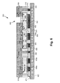
- Figure 2 shows a cross-sectional view of semiconductor package 201 mounted on printed circuit board (PCB) 290 by solder bodies 292 at surface 271 of semiconductor package 201.
- Semiconductor package 201 includes control switch Q 1 implemented as first vertical FET 220 in first or control active die 221, and sync switch Q 2 implemented as second vertical FET 230 in second or sync active die 231.
- First vertical FET 220 includes source 224 and gate 226 on source side 225 of first or control active die 221, as well as drain 222 on drain side 223 of first or control active die 221.
- Second vertical FET 230 includes source 234 and gate 236 on source side 235 of second or sync active die 231, as well as drain 232 on drain side 233 of second or sync active die 231.
- Semiconductor package 201 further includes conductive carriers 210a and 210b having respective surfaces 218a and 218b, electrically conductive die attach material 219, patterned dielectric 240, insulator 282 filling isolation trench 280, and patterned insulator layers 272 and 284.
- conductive carrier 210a may be attached to source side 225 of first active die 221 and to drain side 233 of second active die 231 so as to couple source 224 to drain 232.
- conductive carrier 210b may be attached to gate 226 on source side 225 of first active die 221.
- drain contact 262 Also included in semiconductor package 201 are drain contact 262, source contact 254, gate contact 256, gate contact 266 provided by conductive carrier 210b, switch node contact 250 provided by conductive carrier 210a, and heat spreader 286 mounted to conductive carrier 210a by solder body 288 through surface 285.
- semiconductor package 201 corresponds in general to switching stage 101 in Figure 1 .
- first vertical FET 220 having drain 222, source 224, and gate 226, and second vertical FET 230 having drain 232, source 234, and gate 236, correspond in general to control switch 120 having drain 122, source 124, and gate 126, and sync switch 130 having drain 132, source 134, and gate 136, respectively, in Figure 1 .
- first and second vertical FETs 220 and 230, in Figure 2 may be utilized to implement switching stage 101 of power converter 100, in Figure 1 .
- switch node contact 250 corresponds to switch node 150 of switching stage 101, in Figure 1 .
- FIG. 4A-4G The features of semiconductor package 201 will be now be described in greater detail by reference to Figure 3 , and Figures 4A, 4B , 4C, 4D , 4E, 4F , and 4G (hereinafter “ Figures 4A-4G ").
- Figures 4A-4G the electrical connection between source 224 of first vertical FET 220 and drain 232 of second vertical FET 230 is established in the absence of a conductive clip or other feature implemented solely or primarily as an electrical connector.
- the coupling of source 224 to drain 232 that establishes switch node contact 250 is advantageously provided by conductive carrier 210a and conductive die attach material 219.
- the packaging solution of Figure 2 provides a robust, low resistance, and low parasitic electrical conduction path for providing switch node contact 250.
- inventive concepts disclosed by the packaging solution represented in Figure 2 can be extended to enable the fabrication of high density MCM packages, with reduced parasitics.
- Figure 3 shows flowchart 300 presenting an exemplary method for fabricating a semiconductor package including conductive carrier coupled power switches. It is noted that the method described by flowchart 300 is performed on a conductive carrier, which may be a semiconductor package lead frame, or may take the form of a conductive sheet or plate, for example.
- a conductive carrier which may be a semiconductor package lead frame, or may take the form of a conductive sheet or plate, for example.
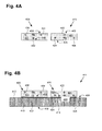
- Figure 4A depicts first and second vertical FETS 420 and 430 (310)
- structure 411 in Figure 4B shows a portion of contiguous conductive carrier 410 attached to first and second vertical FETs 420 and 430 (311)
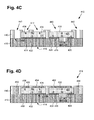
- structure 412 in Figure 4C shows structure 411 after the formation and patterning of a dielectric layer (312), and so forth.
- contiguous conductive carrier 410, in Figures 4B through 4E , and conductive carriers 410a and 410b in Figures 4F and 4G correspond in general to conductive carriers 210a and 210b, in Figure 2 .
- Figures 4A-4G depict formation of a structure including one dielectric layer and one conductive buildup layer, other implementations using the present concepts may include more than one dielectric layer and more than one conductive buildup layer.
- flowchart 300 begins with providing first and second vertical FETs 420 and 430 in respective first and second active dies 421 and 431 (310).
- first vertical FET 420 may be used to provide control switch Q 1 having source 424 and gate 426 on source side 425 of first or control active die 421, and drain 422 on drain side 423 of first or control active die 421.
- Second vertical FET 430 may be used to provide sync switch Q 2 having source 434 and gate 436 on source side 435 of second or sync active die 431, and drain 432 on drain side 433 of second or sync active die 431.
- first and second vertical FETs 420 and 430 providing respective control and sync switches Q 1 and Q 2 may take the form of group IV material based vertical FETs, such as silicon vertical MOSFETs for example.
- control and sync switches Q 1 and Q 2 may take the form of group III-V based power transistors, such as GaN or other III-Nitride based FETs.
- First vertical FET 420 in first or control active die 421 and second vertical FET 430 in second or sync active die 431 correspond respectively to first vertical FET 220 in first or control active die 221 and second vertical FET 230 in second or sync active die 231, in Figure 2 .
- contiguous conductive carrier 410 is represented as a pre-patterned conductive sheet or plate having top surface 408, bottom surface 418, and cavity 409 pre-patterned at top surface 408.
- Contiguous conductive carrier 410 may be formed of any conductive material having a suitably low electrical resistance. Examples of materials from which contiguous conductive carrier 410 may be formed include copper (Cu), aluminum (Al), or a conductive alloy. As noted above, in one implementation, contiguous conductive carrier 410 may be implemented using a semiconductor package lead frame.
- contiguous conductive carrier 410 shows contiguous conductive carrier 410 as a pre-patterned sheet or plate including a single cavity 409 at top surface 408, in other implementations, contiguous conductive carrier 410 may be pre-patterned to have multiple cavities, corresponding to cavity 409, at top surface 408. Furthermore, although the present exemplary implementation shows contiguous conductive carrier 410 as a pre-patterned sheet or plate, that need not always be the case. For example, in other implementations of the present method, an unpatterned conductive sheet or plate from which cavities corresponding to cavity 409 are omitted may be used as contiguous conductive carrier 410.
- contiguous conductive carrier 410 may include a barrier metal layer formed on one or both of top surface 408 and bottom surface 418.
- a barrier metal layer may be formed of nickel-gold (NiAu) or nickel-palladium-gold (NiPdAu), for example.
- such a barrier metal layer may serve as an etching mask during patterning or pre-patterning of contiguous conductive carrier 410. Thereafter, such a barrier metal layer can provide a solderable surface at one or both of top surface 408 and bottom surface 418 of contiguous conductive carrier 410.
- top surface 408 of contiguous conductive carrier 410 is attached to source side 425 of first or control active die 421 and to drain side 433 of second or sync active die 431 by die attach material 419, which, according to the present exemplary implementation is an electrically conductive die attach material.
- die attach material 419 which, according to the present exemplary implementation is an electrically conductive die attach material.
- first or control active die 421 and second or sync active die 431 are flipped relative to each other. That is to say, second or sync active die 431 is disposed on contiguous conductive carrier 410 in a "face up” orientation in which drain 432 is attached to top surface 408, while first or control active die 421 is oriented "face down” such that source 424 and gate 426 are attached to top surface 408.
- first or control active die 421 is disposed over cavity 409 such that cavity 409 is situated between the attachment of source 424 to top surface 408 and the attachment of gate 426 to top surface 408, by electrically conductive die attach material 419.
- Electrically conductive die attach material 419 may be any suitable substance, such as a conductive epoxy, solder, a conductive sintered material, or diffusion bonded material, and may be formed to a thickness of from approximately 0.5 mm to approximately 2.0 mm, for example. Electrically conductive die attach material 419 corresponds to electrically conductive die attach material 219, in Figure 2 , while contiguous conductive carrier 410, in Figure 4B , corresponds in general to, and serves as a foundational structure for, conductive carriers 210a and 210b, in Figure 2 .
- flowchart 300 continues with forming a dielectric layer over contiguous conductive carrier 410, first or control active die 421, and second or sync active die 431, followed by patterning of the dielectric layer to form patterned dielectric 440 (312).
- Patterned dielectric 440 may be formed by initially laminating a pre-formed dielectric layer onto contiguous conductive carrier 410, first or control active die 421, and second or sync active die 431, and then patterning the pre-formed dielectric layer to produce windows 442.
- Such a pre-formed dielectric layer may be cut or otherwise patterned from a pre-formable dielectric material, such as an epoxy-phenolic or cyanate ester-epoxy build-up material, for example, or any other pre-formable dielectric utilized in laminate substrate technology.
- patterned dielectric 440 may be formed of a B-stage polymeric material cured during lamination. As a result, pre-formed dielectric 440 can substantially fill cavity 409, as shown in Figure 4C .
- Patterning of the dielectric layer to form patterned dielectric 440 including windows 442 can be performed using any known technique, such as etching.
- Patterned dielectric 440 includes windows 442 exposing top surface 408 of contiguous conductive carrier 410 adjacent each of first or control active die 421 and second or sync active die 431, as well as windows 442 exposing drain 422, source 434, and gate 436.
- Patterned dielectric 440 corresponds to patterned dielectric 240, in Figure 2 .
- flowchart 300 continues with buildup of a conductive layer over patterned dielectric 440, and patterning of the conductive layer to form contacts 462, 466, 450, 454, and 456 (313).
- the conductive layer may be formed of Cu or Al, for example, or may be a metal alloy, such as a metal alloy including Cu and Ni, for example. Such a conductive layer may be built up using any suitable technique, such as electrochemical deposition or an electrolytic plating process, for example.
- the conductive layer is patterned to form drain contact 462, gate contacts 466 and 456, switch node contact 450, and source contact 454. Drain contact 462, gate contacts 466 and 456, switch node contact 450, and source contact 454 correspond respectively to drain contact 262, gate contacts 266 and 256, switch node contact 250, and source contact 254, in Figure 2 .
- flowchart 300 continues with forming an insulator layer over patterned dielectric 440 and contacts 462, 466, 450, 454, and 456, and patterning the insulator layer to expose contacts 462, 466, 450, 454, and 456 (314).
- the insulator layer may be formed as a blanket layer of solder resist, for example, which is thereafter patterned to form patterned insulator layer 472 providing surface 471. Patterned insulator layer 472 providing surface 471 corresponds to patterned insulator layer 272 providing surface 271, in Figure 2 .
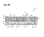
- isolation trench 480 is formed at bottom surface 418 of contiguous conductive carrier 410 and extends from bottom surface 418 to patterned dielectric 440 formed in cavity 409 at top surface 408. Moreover, in some implementations, as shown in Figure 4F , isolation trench 480 may be substantially aligned with cavity 409.
- Isolation trench 480 may be formed using any suitable technique, such as etching, or laser ablation, for example, as known in the art. Formation of isolation trench 480 results in electrical isolation of conductive carrier 410a from conductive carrier 410b. Isolation trench 480 and conductive carriers 410a and 410b having respective bottom surfaces 418a and 418b correspond respectively to isolation trench 280 and conductive carriers 210a and 210b having respective surfaces 218a and 218b, in Figure 2 .
- isolation trench 480 extends from bottom surface 418 of contiguous conductive carrier 410 to patterned dielectric 440 within cavity 409, that feature results from use of a pre-patterned contiguous conductive carrier 410.
- cavity 409 and its dielectric fill would typically be absent, and isolation trench 480 could be formed so as to extend from bottom surface 418, through contiguous conductive carrier 410, to top surface 408.
- isolation trench 480 could be formed through conductive carrier 410 so as to form a gap between the attachment of source 424 to top surface 408 and the attachment of gate 426 to top surface 408.
- the method of flowchart 300 may optionally continue with filling of isolation trench 480 with insulator 482 (316).
- isolation trench 480 alone may be sufficient to provide electrical isolation between conductive carriers 410a and 410b, without the need for a dielectric fill.
- Insulator 482 may be formed of solder resist, for example, and may be deposited or otherwise formed so as to fill isolation trench 480, as well as to provide surface 485. Insulator 482 providing surface 485 corresponds to insulator 282 providing surface 285, in Figure 2 .
- the method of flowchart 300 may conclude with utilizing conductive carrier 410a formed from contiguous conductive carrier 410 to provide switch node contact 450 for a semiconductor package including first and second vertical FETs 420 and 430 (317).
- conductive carrier 410a couples source 424 of first vertical FET 420 to drain 432 of second vertical FET 430, and is isolated from gate 426 of first vertical FET 420 by isolation trench 480.
- conductive carrier 210a/410a can be used to provide switch node contact 250/450, which in turn is configured to provide an output node of semiconductor package 201 accessible through surface 271/471. Consequently, the electrical connection between source 224/424 of first vertical FET 220/420 and drain 232/432 of second vertical FET 230/430 may be established in the absence of a conductive clip or other feature implemented solely or primarily as an electrical connector.
- the exemplary method of flowchart 300 enables fabrication of a semiconductor package including a robust, low resistance, and low parasitic electrical conduction path for providing switch node contact 250/450.
- FIG. 5 depicts an exemplary semiconductor package including conductive carrier coupled power switches and a driver IC for driving one or both of the power switches, according to one implementation.
- FIG. 5 depicts an exemplary semiconductor package including conductive carrier coupled power switches and a driver IC for driving one or both of the power switches, according to one implementation.
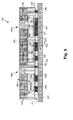
- FIG. 5 shows a cross-sectional view of MCM 502 mounted on PCB 590 by solder bodies 592 at surface 571 of MCM 502.
- MCM 502 includes control active die 521 providing vertical FET 520 having drain 522, source 524, and gate 526, and implementing control switch Q 1 .
- MCM 502 includes sync active die 531 providing vertical FET 530 having drain 532, source 534, and gate 536, and implementing sync switch Q 2 .
- MCM 502 also includes driver IC 594 for driving one or both of control and sync switches Q 1 and Q 2 .
- MCM 502 further includes conductive carriers 510a, 510b, and 510c having respective surfaces 518a, 518b, and 518c, electrically conductive die attach material 519, patterned dielectric 540, insulator 582 partially filling isolation trenches 580a and 580b and forming an insulation layer at surface 585, and patterned insulator layer 572 providing surface 571. It is noted that the respective portions of isolation trenches 580a and 580b not filled by insulator 582 are filled by patterned dielectric 540.
- drain contact 562 Also included in MCM 502 are drain contact 562, source contact, 554, gate contacts 566 and 556, switch node contact 550, input/output (I/O) pads 596a and 596b of driver IC 594, and die attach material 593 for attaching driver IC 594 to conductive carrier 510c.
- I/O input/output
- die attach material 593 may be an electrically conductive die attach material.
- die attach material 593 may be a dielectric die attach material, thereby providing additional electrical isolation between conductive carrier 510c and driver IC 594.
- Conductive carriers 510a and 510b, vertical FETs 520 and 530, and electrically conductive die attach material 519 correspond respectively to conductive carriers 210a and 210b, first and second vertical FETs 220 and 230, and electrically conductive die attach material 219, in Figure 2 .
- patterned dielectric 540, isolation trench 580a, insulator 582, contacts 562, 566, 550, 554, and 556, and patterned insulator layer 572, in Figure 5 correspond respectively to patterned dielectric 240, isolation trench 280, insulator 282, contacts 262, 266, 250, 254, and 256, and patterned insulator layer 272, in Figure 2 .
- MCM 502 including driver IC 594 corresponds in general to MCM 102 including driver IC 194, in Figure 1 .
- conductive carrier 510a advantageously provides switch node contact 550 and thereby couples source 524 of vertical FET 520 to drain 532 of vertical FET 530.
- Isolation trench 580a provides electrical isolation between conductive carrier 510b, providing gate contact 566 of vertical FET 520, and conductive carrier 510a providing switch node contact 550.
- isolation trench 580b protects driver IC 594 from switching noise that may be present in conductive carrier 510a by electrically isolating conductive carrier 510a from conductive carrier 510c, to which driver IC 594 is attached.
- MCM 502 may include a heat spreader.
- a heat spreader corresponding to heat spreader 286 in Figure 2 may be attached to conductive carrier 510c and/or conductive carrier 510a through insulator 582 providing surface 585.
- Figure 6 shows a cross-sectional view of an exemplary semiconductor package including conductive carrier coupled power switches and a driver IC for driving one or both of the power switches, according to another implementation.
- MCM 602 mounted on PCB 690 by solder bodies 692 at surface 671 of MCM 602.
- MCM 602 includes control active die 621 providing vertical FET 620 having drain 622, source 624, and gate 626, and implementing control switch Q 1 .
- MCM 602 includes sync active die 631 providing vertical FET 630 having drain 632, source 634, and gate 636, and implementing sync switch Q 2 .
- MCM 602 also includes driver IC 694 for driving one or both of control and sync switches Q 1 and Q 2 .
- MCM 602 further includes conductive carriers 610a and 610b having respective surfaces 618a and 618b, electrically conductive die attach material 619, patterned dielectric 640, and patterned insulator layer 672 providing surface 671. It is noted that isolation trench 680 is partially filled by patterned dielectric 640. Also included in MCM 602 are drain contact 662, source contact 654, gate contacts 666 and 656, switch node contact 650, input/output (I/O) pads 696a and 696b of driver IC 694, and die attach material 693 for attaching driver IC 694 to conductive carrier 610a.
- I/O input/output
- Conductive carriers 610a and 610b, vertical FETs 620 and 630, and electrically conductive die attach material 619 correspond respectively to conductive carriers 210a and 210b, first and second vertical FETs 220 and 230, and electrically conductive die attach material 219, in Figure 2 .
- patterned dielectric 640, isolation trench 680, contacts 662, 666, 650, 654, and 656, and patterned insulator layer 672, in Figure 6 correspond respectively to patterned dielectric 240, isolation trench 280, contacts 262, 266, 250, 254, and 256, and patterned insulator layer 272, in Figure 2 .
- die attach material 693, in Figure 6 corresponds to die attach material 593, in Figure 5 .
- MCM 602 including driver IC 694, in Figure 6 corresponds in general to MCM 102 including driver IC 194, in Figure 1 .
- conductive carrier 610a advantageously provides switch node contact 650 and thereby couples source 624 of vertical FET 620 to drain 632 of vertical FET 630.
- isolation trench 680 provides electrical isolation between conductive carrier 610b, providing gate contact 666 of vertical FET 620, and conductive carrier 610a providing switch node contact 650.
- MCM 602 may include a heat spreader.
- a heat spreader corresponding to heat spreader 286 in Figure 2 may be attached to conductive carrier 610a at surface 618a.
- the packaging solutions disclosed herein advantageously enable a highly compact package design.
- the present solution enables omission of a conductive clip, or any other feature implemented solely or primarily as a switch node electrical connector, from an MCM package.
- implementations of the present solution advantageously provide a reliable, low resistance, and substantially parasitic free electrical connection for establishing a power converter switch node.
Landscapes
- Dc-Dc Converters (AREA)
Abstract
Description
- The present application claims the benefit of and priority to a provisional application entitled "Semiconductor Package Including Lead Frame Coupled Power Switches," Serial No.
61/715,662 filed on October 18, 2012 - Power converters are used in a variety of electronic circuits and systems. Many integrated circuit (IC) applications, for instance, require conversion of a direct current (DC) input to a lower, or higher, DC output. For example, a synchronous buck converter may be implemented as a voltage regulator to convert a higher voltage DC input to a lower voltage DC output for use in low voltage applications in which relatively large output currents are required.
- The voltage converted output of a synchronous buck converter is typically provided through a switch node situated between a high side control switch and a low side synchronous (sync) switch of the power converter switching stage. The electrical connection between the control and sync power switches may be implemented using a conductive clip, such as a copper clip, which must be sufficiently robust to accommodate high current. Moreover, because the control and sync power switches can be very sensitive to electrical resistance, the cross-sectional area of the conductive clip used to provide the switch node is often relatively large. Consequently, packaging solutions for such power converters must typically be sized to accommodate not only the control and sync switches of the power converter switching stage, but a relatively large conductive clip for connection of those power switches as well.
- The present disclosure is directed to a semiconductor package including conductive carrier coupled power switches, substantially as shown in and/or described in connection with at least one of the figures, and as set forth more completely in the claims.
-
-
Figure 1 shows a diagram of an exemplary power converter circuit. -
Figure 2 shows a cross-sectional view of an exemplary semiconductor package including conductive carrier coupled power switches, according to one implementation. -
Figure 3 shows a flowchart presenting one exemplary method for fabricating a semiconductor package including conductive carrier coupled power switches. -
Figure 4A depicts an initial stage of the method described inFigure 3 . -
Figure 4B shows an exemplary structure corresponding to an intermediate stage of the method described inFigure 3 . -
Figure 4C shows the exemplary structure inFigure 4B at another intermediate stage of the fabrication method described inFigure 3 . -
Figure 4D shows the exemplary structure inFigure 4C at another intermediate stage of the fabrication method described inFigure 3 . -
Figure 4E shows the exemplary structure inFigure 4D at another intermediate stage of the fabrication method described inFigure 3 . -
Figure 4F shows the exemplary structure inFigure 4E at another intermediate stage of the fabrication method described inFigure 3 . -
Figure 4G shows the exemplary structure inFigure 4F at another intermediate stage of the fabrication method described inFigure 3 . -
Figure 5 shows a cross-sectional view of an exemplary semiconductor package including conductive carrier coupled power switches and a driver integrated circuit (IC) for driving one or both of the power switches, according to one implementation. -
Figure 6 shows a cross-sectional view of an exemplary semiconductor package including conductive carrier coupled power switches and a driver IC for driving one or both of the power switches, according to another implementation. - The following description contains specific information pertaining to implementations in the present disclosure. One skilled in the art will recognize that the present disclosure may be implemented in a manner different from that specifically discussed herein. The drawings in the present application and their accompanying detailed description are directed to merely exemplary implementations. Unless noted otherwise, like or corresponding elements among the figures may be indicated by like or corresponding reference numerals. Moreover, the drawings and illustrations in the present application are generally not to scale, and are not intended to correspond to actual relative dimensions.
- As stated above, power converters such as voltage regulators are used in a variety of electronic circuits and systems. For instance, and as noted above, integrated circuit (IC) applications may require conversion of a direct current (DC) input to a lower, or higher, DC output. As a specific example, a buck converter may be implemented as a voltage regulator to convert a higher voltage DC input to a lower voltage DC output for use in low voltage applications in which relatively large output currents are required.
-
Figure 1 shows a diagram of an exemplary power converter circuit.Power converter 100 includes power converter multi-chip module (MCM) 102,output inductor 104, andoutput capacitor 106. As shown inFigure 1 ,MCM 102 includesswitching stage 101 ofpower converter 100, and driver IC 194 implemented to provide drive signals to switchingstage 101. As shown inFigure 1 ,power converter 100 is configured to receive an input voltage VIN, and to provide a converted voltage, e.g., a rectified and/or stepped down voltage, as VOUT atoutput 105. -
Switching stage 101 may be implemented using two power switches in the form of metal-oxide-semiconductor field-effect transistors (MOSFETs) configured as a half bridge, for example. That is to say, switchingstage 101 may include high side or control switch 120 (Q1) havingdrain 122,source 124, andgate 126, as well as low side or synchronous (sync) switch 130 (Q2) havingdrain 132,source 134, andgate 136.Control switch 120 is coupled withsync switch 130 atswitch node 150, which, in turn, is coupled tooutput 105 throughoutput inductor 104. Respective control andsync switches Power converter 100 may be advantageously utilized as a voltage converter, for example a buck converter, in a variety of automotive, industrial, appliance, and lighting applications. - It is noted that in the interests of ease and conciseness of description, the present inventive principles will in some instances be described by reference to specific implementations of a buck converter including one or more silicon based power transistors. However, it is emphasized that such implementations are merely exemplary, and the inventive principles disclosed herein are broadly applicable to a wide range of applications, including buck and boost converters, implemented using other group IV material based, or group III-V semiconductor based, power transistors. It is noted that as used herein, the phrase "group III-V" refers to a compound semiconductor including at least one group III element and at least one group V element. By way of example, a group III-V semiconductor may take the form of a III-Nitride semiconductor that includes nitrogen and at least one group III element. For instance, a III-Nitride power transistor may be fabricated using gallium nitride (GaN), in which the group III element or elements include some or a substantial amount of gallium, but may also include other group III elements in addition to gallium.
- As noted above, the connection between
control switch 120 andsync switch 130 providingswitch node 150 can be implemented using a conductive clip, such as a copper clip, which must be sufficiently robust to accommodate high current. Moreover, becausecontrol switch 120 andsync switch 130 can be very sensitive to electrical resistance, the cross-sectional area of the conductive clip used to provideswitch node 150 is often relatively large. Consequently, packaging solutions for power converters, such as a power switching module containingswitching stage 101, or MCM 102 includingswitching stage 101 and driver IC 194, must be sized to accommodate a large conductive clip for connection of the power switches. - The present application discloses a packaging solution enabling omission of such a conductive clip, or any other feature implemented solely or primarily as a switch node electrical connector, while concurrently providing a reliable, low resistance, and substantially parasitic free electrical connection for establishing
switch node 150. In one implementation, a conductive carrier utilized as a structural support in the packaging solution, such as a conductive lead frame for example, is configured tocouple control switch 120 tosync switch 130 so as to provideswitch node 150. In one such implementation, the conductive carrier may provide a substantially direct electrical connection betweensource 124 ofcontrol switch 120 anddrain 132 ofsync switch 130.Figure 2 shows an exemplary representation of such a packaging solution. -
Figure 2 shows a cross-sectional view ofsemiconductor package 201 mounted on printed circuit board (PCB) 290 bysolder bodies 292 atsurface 271 ofsemiconductor package 201.Semiconductor package 201 includes control switch Q1 implemented as firstvertical FET 220 in first or controlactive die 221, and sync switch Q2 implemented as second vertical FET 230 in second or syncactive die 231. First vertical FET 220 includessource 224 and gate 226 onsource side 225 of first or controlactive die 221, as well asdrain 222 ondrain side 223 of first or controlactive die 221. Second vertical FET 230 includessource 234 andgate 236 onsource side 235 of second or syncactive die 231, as well asdrain 232 ondrain side 233 of second or syncactive die 231. -
Semiconductor package 201 further includesconductive carriers respective surfaces 218a and 218b, electrically conductivedie attach material 219, patterned dielectric 240,insulator 282 filling isolation trench 280, and patternedinsulator layers Figure 2 ,conductive carrier 210a may be attached tosource side 225 of firstactive die 221 and to drainside 233 of secondactive die 231 so as tocouple source 224 to drain 232. As further shown inFigure 2 ,conductive carrier 210b may be attached to gate 226 onsource side 225 of firstactive die 221. Also included insemiconductor package 201 are draincontact 262,source contact 254,gate contact 256,gate contact 266 provided byconductive carrier 210b,switch node contact 250 provided byconductive carrier 210a, andheat spreader 286 mounted toconductive carrier 210a bysolder body 288 throughsurface 285. -
Semiconductor package 201 corresponds in general to switchingstage 101 inFigure 1 . In addition, firstvertical FET 220 havingdrain 222,source 224, and gate 226, and second vertical FET 230 havingdrain 232,source 234, andgate 236, correspond in general to controlswitch 120 havingdrain 122,source 124, andgate 126, andsync switch 130 havingdrain 132,source 134, andgate 136, respectively, inFigure 1 . In other words, first and secondvertical FETs 220 and 230, inFigure 2 , may be utilized to implement switchingstage 101 ofpower converter 100, inFigure 1 . Moreover,switch node contact 250, inFigure 2 , corresponds to switchnode 150 of switchingstage 101, inFigure 1 . - The features of
semiconductor package 201 will be now be described in greater detail by reference toFigure 3 , andFigures 4A, 4B ,4C, 4D ,4E, 4F , and4G (hereinafter "Figures 4A-4G "). However, it is noted in reference toFigure 2 that the electrical connection betweensource 224 of firstvertical FET 220 and drain 232 of second vertical FET 230 is established in the absence of a conductive clip or other feature implemented solely or primarily as an electrical connector. Instead, according to the implementation shown inFigure 2 , the coupling ofsource 224 to drain 232 that establishesswitch node contact 250 is advantageously provided byconductive carrier 210a and conductive die attachmaterial 219. As a result, the packaging solution ofFigure 2 provides a robust, low resistance, and low parasitic electrical conduction path for providingswitch node contact 250. Moreover, the inventive concepts disclosed by the packaging solution represented inFigure 2 can be extended to enable the fabrication of high density MCM packages, with reduced parasitics. - Referring to
Figure 3, Figure 3 showsflowchart 300 presenting an exemplary method for fabricating a semiconductor package including conductive carrier coupled power switches. It is noted that the method described byflowchart 300 is performed on a conductive carrier, which may be a semiconductor package lead frame, or may take the form of a conductive sheet or plate, for example. - With respect to
Figures 4A-4G , those figures illustrate the result of performing the method offlowchart 300. For example,Figure 4A depicts first and secondvertical FETS 420 and 430 (310),structure 411 inFigure 4B shows a portion of contiguousconductive carrier 410 attached to first and secondvertical FETs 420 and 430 (311),structure 412 inFigure 4C showsstructure 411 after the formation and patterning of a dielectric layer (312), and so forth. It is noted that contiguousconductive carrier 410, inFigures 4B through 4E , andconductive carriers Figures 4F and4G , correspond in general toconductive carriers Figure 2 . It is further noted that althoughFigures 4A-4G depict formation of a structure including one dielectric layer and one conductive buildup layer, other implementations using the present concepts may include more than one dielectric layer and more than one conductive buildup layer. - Referring to
flowchart 300, inFigure 3 , in combination withFigure 4A ,flowchart 300 begins with providing first and secondvertical FETs Figure 4A , in one implementation, firstvertical FET 420 may be used to provide control switch Q1 having source 424 andgate 426 onsource side 425 of first or controlactive die 421, and drain 422 ondrain side 423 of first or controlactive die 421. Secondvertical FET 430 may be used to provide sync switch Q2 having source 434 andgate 436 onsource side 435 of second or syncactive die 431, and drain 432 ondrain side 433 of second or syncactive die 431. - In one implementation, first and second
vertical FETs vertical FET 420 in first or controlactive die 421 and secondvertical FET 430 in second or syncactive die 431 correspond respectively to firstvertical FET 220 in first or controlactive die 221 and second vertical FET 230 in second or syncactive die 231, inFigure 2 . - Moving to structure 411 in
Figure 4B with ongoing reference toFigure 3 ,flowchart 300 continues with attaching contiguousconductive carrier 410 to sourceside 425 of first or controlactive die 421 and to drainside 433 of second or sync active die 431 (311). As shown inFigure 4B , contiguousconductive carrier 410 is represented as a pre-patterned conductive sheet or plate havingtop surface 408,bottom surface 418, andcavity 409 pre-patterned attop surface 408. Contiguousconductive carrier 410 may be formed of any conductive material having a suitably low electrical resistance. Examples of materials from which contiguousconductive carrier 410 may be formed include copper (Cu), aluminum (Al), or a conductive alloy. As noted above, in one implementation, contiguousconductive carrier 410 may be implemented using a semiconductor package lead frame. - Although the present exemplary implementation shows contiguous
conductive carrier 410 as a pre-patterned sheet or plate including asingle cavity 409 attop surface 408, in other implementations, contiguousconductive carrier 410 may be pre-patterned to have multiple cavities, corresponding tocavity 409, attop surface 408. Furthermore, although the present exemplary implementation shows contiguousconductive carrier 410 as a pre-patterned sheet or plate, that need not always be the case. For example, in other implementations of the present method, an unpatterned conductive sheet or plate from which cavities corresponding tocavity 409 are omitted may be used as contiguousconductive carrier 410. - Moreover, although not shown in the present figures, in some implementations, contiguous
conductive carrier 410, whether pre-patterned or unpatterned, may include a barrier metal layer formed on one or both oftop surface 408 andbottom surface 418. Such a barrier metal layer may be formed of nickel-gold (NiAu) or nickel-palladium-gold (NiPdAu), for example. In some implementations, such a barrier metal layer may serve as an etching mask during patterning or pre-patterning of contiguousconductive carrier 410. Thereafter, such a barrier metal layer can provide a solderable surface at one or both oftop surface 408 andbottom surface 418 of contiguousconductive carrier 410. - As shown in
Figure 4B ,top surface 408 of contiguousconductive carrier 410 is attached to sourceside 425 of first or controlactive die 421 and to drainside 433 of second or syncactive die 431 by die attachmaterial 419, which, according to the present exemplary implementation is an electrically conductive die attach material. It is noted that first or controlactive die 421 and second or syncactive die 431 are flipped relative to each other. That is to say, second or syncactive die 431 is disposed on contiguousconductive carrier 410 in a "face up" orientation in which drain 432 is attached totop surface 408, while first or controlactive die 421 is oriented "face down" such thatsource 424 andgate 426 are attached totop surface 408. Moreover, and as further shown inFigure 4B , first or controlactive die 421 is disposed overcavity 409 such thatcavity 409 is situated between the attachment ofsource 424 totop surface 408 and the attachment ofgate 426 totop surface 408, by electrically conductive die attachmaterial 419. - Electrically conductive die attach
material 419 may be any suitable substance, such as a conductive epoxy, solder, a conductive sintered material, or diffusion bonded material, and may be formed to a thickness of from approximately 0.5 mm to approximately 2.0 mm, for example. Electrically conductive die attachmaterial 419 corresponds to electrically conductive die attachmaterial 219, inFigure 2 , while contiguousconductive carrier 410, inFigure 4B , corresponds in general to, and serves as a foundational structure for,conductive carriers Figure 2 . - As shown by
structure 412 inFigure 4C ,flowchart 300 continues with forming a dielectric layer over contiguousconductive carrier 410, first or controlactive die 421, and second or syncactive die 431, followed by patterning of the dielectric layer to form patterned dielectric 440 (312). Patterned dielectric 440 may be formed by initially laminating a pre-formed dielectric layer onto contiguousconductive carrier 410, first or controlactive die 421, and second or syncactive die 431, and then patterning the pre-formed dielectric layer to producewindows 442. Such a pre-formed dielectric layer may be cut or otherwise patterned from a pre-formable dielectric material, such as an epoxy-phenolic or cyanate ester-epoxy build-up material, for example, or any other pre-formable dielectric utilized in laminate substrate technology. In one implementation, for example, patterneddielectric 440 may be formed of a B-stage polymeric material cured during lamination. As a result,pre-formed dielectric 440 can substantially fillcavity 409, as shown inFigure 4C . - Patterning of the dielectric layer to form patterned dielectric 440 including
windows 442 can be performed using any known technique, such as etching. Patterned dielectric 440 includeswindows 442 exposingtop surface 408 of contiguousconductive carrier 410 adjacent each of first or controlactive die 421 and second or syncactive die 431, as well aswindows 442 exposingdrain 422,source 434, andgate 436. Patterned dielectric 440 corresponds to patterneddielectric 240, inFigure 2 . - Moving to structure 413 in
Figure 4D ,flowchart 300 continues with buildup of a conductive layer over patterneddielectric 440, and patterning of the conductive layer to formcontacts drain contact 462,gate contacts switch node contact 450, andsource contact 454.Drain contact 462,gate contacts switch node contact 450, and source contact 454 correspond respectively to draincontact 262,gate contacts switch node contact 250, andsource contact 254, inFigure 2 . - Continuing to structure 414 in
Figure 4E ,flowchart 300 continues with forming an insulator layer over patterneddielectric 440 andcontacts contacts insulator layer 472 providingsurface 471.Patterned insulator layer 472 providingsurface 471 corresponds to patternedinsulator layer 272 providingsurface 271, inFigure 2 . - Moving to structure 415 in
Figure 4F ,flowchart 300 continues with formingisolation trench 480 through contiguous conductive carrier 410 (315).Isolation trench 480 is formed atbottom surface 418 of contiguousconductive carrier 410 and extends frombottom surface 418 to patterned dielectric 440 formed incavity 409 attop surface 408. Moreover, in some implementations, as shown inFigure 4F ,isolation trench 480 may be substantially aligned withcavity 409. -
Isolation trench 480 may be formed using any suitable technique, such as etching, or laser ablation, for example, as known in the art. Formation ofisolation trench 480 results in electrical isolation ofconductive carrier 410a fromconductive carrier 410b.Isolation trench 480 andconductive carriers respective bottom surfaces 418a and 418b correspond respectively to isolation trench 280 andconductive carriers respective surfaces 218a and 218b, inFigure 2 . - It is noted that although in the present exemplary implementation,
isolation trench 480 extends frombottom surface 418 of contiguousconductive carrier 410 to patterneddielectric 440 withincavity 409, that feature results from use of a pre-patterned contiguousconductive carrier 410. In implementations in which an unpatterned conductive carrier is used,cavity 409 and its dielectric fill would typically be absent, andisolation trench 480 could be formed so as to extend frombottom surface 418, through contiguousconductive carrier 410, totop surface 408. In those implementations,isolation trench 480 could be formed throughconductive carrier 410 so as to form a gap between the attachment ofsource 424 totop surface 408 and the attachment ofgate 426 totop surface 408. - Turning now to structure 416 in
Figure 4G , in some implementations, the method offlowchart 300 may optionally continue with filling ofisolation trench 480 with insulator 482 (316). In some implementations, as shown inFigure 4G ,isolation trench 480 alone may be sufficient to provide electrical isolation betweenconductive carriers isolation trenches 480 with a suitable electrically insulating material.Insulator 482 may be formed of solder resist, for example, and may be deposited or otherwise formed so as to fillisolation trench 480, as well as to providesurface 485.Insulator 482 providingsurface 485 corresponds to insulator 282 providingsurface 285, inFigure 2 . - The method of
flowchart 300 may conclude with utilizingconductive carrier 410a formed from contiguousconductive carrier 410 to provideswitch node contact 450 for a semiconductor package including first and secondvertical FETs 420 and 430 (317). As shown inFigures 4F and4G ,conductive carrier 410a couples source 424 of firstvertical FET 420 to drain 432 of secondvertical FET 430, and is isolated fromgate 426 of firstvertical FET 420 byisolation trench 480. - Referring to
Figure 2 in combination withFigures 4F and4G ,conductive carrier 210a/410a can be used to provideswitch node contact 250/450, which in turn is configured to provide an output node ofsemiconductor package 201 accessible throughsurface 271/471. Consequently, the electrical connection betweensource 224/424 of firstvertical FET 220/420 and drain 232/432 of second vertical FET 230/430 may be established in the absence of a conductive clip or other feature implemented solely or primarily as an electrical connector. Thus, the exemplary method offlowchart 300 enables fabrication of a semiconductor package including a robust, low resistance, and low parasitic electrical conduction path for providingswitch node contact 250/450. - Although the implementations shown and described by reference to
Figures 2 ,3 , and4A-4G result in an MCM, such assemiconductor package 201, inFigure 2 , configured to enclose switchingstage 101, inFigure 1 , in some applications, it may be desirable to produce a semiconductor package corresponding toMCM 102. An example implementation of such an MCM package is shown byFigure 5 , which depicts an exemplary semiconductor package including conductive carrier coupled power switches and a driver IC for driving one or both of the power switches, according to one implementation. One of ordinary skill in the art will readily understand that the exemplary method outlined byflowchart 300, inFigure 3 , can be suitably adapted to produce the exemplary MCM package structure shown inFigure 5 . -
Figure 5 shows a cross-sectional view ofMCM 502 mounted onPCB 590 bysolder bodies 592 atsurface 571 ofMCM 502.MCM 502 includes controlactive die 521 providing vertical FET 520 havingdrain 522,source 524, andgate 526, and implementing control switch Q1. In addition,MCM 502 includes syncactive die 531 providing vertical FET 530 havingdrain 532,source 534, andgate 536, and implementing sync switch Q2. MCM 502 also includesdriver IC 594 for driving one or both of control and sync switches Q1 and Q2. -
MCM 502 further includesconductive carriers respective surfaces dielectric 540,insulator 582 partially fillingisolation trenches surface 585, and patternedinsulator layer 572 providingsurface 571. It is noted that the respective portions ofisolation trenches insulator 582 are filled by patterneddielectric 540. Also included inMCM 502 aredrain contact 562, source contact, 554,gate contacts switch node contact 550, input/output (I/O)pads driver IC 594, and die attachmaterial 593 for attachingdriver IC 594 toconductive carrier 510c. - According to the present implementation, the absence of I/O pads on
side 595 ofdriver IC 594, as well as the insulating properties of any encapsulant or packaging ofdriver IC 594 may be sufficient to isolatedriver IC 594 fromconductive carrier 510c, to whichdriver IC 594 is attached. As a result, in some implementations, die attachmaterial 593 may be an electrically conductive die attach material. However, in some implementations, die attachmaterial 593 may be a dielectric die attach material, thereby providing additional electrical isolation betweenconductive carrier 510c anddriver IC 594. -
Conductive carriers 510a and 510b, vertical FETs 520 and 530, and electrically conductive die attach material 519 correspond respectively toconductive carriers vertical FETs 220 and 230, and electrically conductive die attachmaterial 219, inFigure 2 . In addition, patterneddielectric 540,isolation trench 580a,insulator 582,contacts insulator layer 572, inFigure 5 , correspond respectively to patterneddielectric 240, isolation trench 280,insulator 282,contacts insulator layer 272, inFigure 2 . Moreover, it is noted thatMCM 502 includingdriver IC 594, inFigure 5 , corresponds in general toMCM 102 includingdriver IC 194, inFigure 1 . - According to the implementation shown in
Figure 5 , conductive carrier 510a advantageously providesswitch node contact 550 and thereby couples source 524 of vertical FET 520 to drain 532 of vertical FET 530.Isolation trench 580a provides electrical isolation betweenconductive carrier 510b, providinggate contact 566 of vertical FET 520, and conductive carrier 510a providingswitch node contact 550. Moreoverisolation trench 580b protectsdriver IC 594 from switching noise that may be present in conductive carrier 510a by electrically isolating conductive carrier 510a fromconductive carrier 510c, to whichdriver IC 594 is attached. - It is noted that although not shown in
Figure 5 , in some implementations,MCM 502 may include a heat spreader. For example, a heat spreader corresponding to heatspreader 286 inFigure 2 may be attached toconductive carrier 510c and/or conductive carrier 510a throughinsulator 582 providingsurface 585. - Referring now to
Figure 6, Figure 6 shows a cross-sectional view of an exemplary semiconductor package including conductive carrier coupled power switches and a driver IC for driving one or both of the power switches, according to another implementation.Figure 6 showsMCM 602 mounted onPCB 690 bysolder bodies 692 atsurface 671 ofMCM 602.MCM 602 includes controlactive die 621 providingvertical FET 620 havingdrain 622,source 624, and gate 626, and implementing control switch Q1. In addition,MCM 602 includes syncactive die 631 providingvertical FET 630 having drain 632,source 634, andgate 636, and implementing sync switch Q2. MCM 602 also includesdriver IC 694 for driving one or both of control and sync switches Q1 and Q2. -
MCM 602 further includesconductive carriers material 619, patterneddielectric 640, and patternedinsulator layer 672 providingsurface 671. It is noted thatisolation trench 680 is partially filled by patterneddielectric 640. Also included inMCM 602 aredrain contact 662,source contact 654,gate contacts switch node contact 650, input/output (I/O)pads driver IC 694, and die attachmaterial 693 for attachingdriver IC 694 toconductive carrier 610a. -
Conductive carriers vertical FETs material 619 correspond respectively toconductive carriers vertical FETs 220 and 230, and electrically conductive die attachmaterial 219, inFigure 2 . In addition, patterneddielectric 640,isolation trench 680,contacts insulator layer 672, inFigure 6 , correspond respectively to patterneddielectric 240, isolation trench 280,contacts insulator layer 272, inFigure 2 . Moreover, die attachmaterial 693, inFigure 6 , corresponds to die attachmaterial 593, inFigure 5 . Furthermore, it is noted thatMCM 602 includingdriver IC 694, inFigure 6 , corresponds in general toMCM 102 includingdriver IC 194, inFigure 1 . - As shown in
Figure 6 ,conductive carrier 610a advantageously providesswitch node contact 650 and thereby couples source 624 ofvertical FET 620 to drain 632 ofvertical FET 630. In addition,isolation trench 680 provides electrical isolation betweenconductive carrier 610b, providinggate contact 666 ofvertical FET 620, andconductive carrier 610a providingswitch node contact 650. It is noted that although not shown inFigure 6 , in some implementations,MCM 602 may include a heat spreader. For example, a heat spreader corresponding to heatspreader 286 inFigure 2 may be attached toconductive carrier 610a at surface 618a. - Thus, by configuring a conductive carrier utilized as a structural support to couple a control switch and a sync switch of a power converter switching stage, the packaging solutions disclosed herein advantageously enable a highly compact package design. In addition, by configuring the control and sync switches to be flipped relative to one another, the present solution enables omission of a conductive clip, or any other feature implemented solely or primarily as a switch node electrical connector, from an MCM package. Moreover, implementations of the present solution advantageously provide a reliable, low resistance, and substantially parasitic free electrical connection for establishing a power converter switch node.
- From the above description it is manifest that various techniques can be used for implementing the concepts described in the present application without departing from the scope of those concepts. Moreover, while the concepts have been described with specific reference to certain implementations, a person of ordinary skill in the art would recognize that changes can be made in form and detail without departing from the scope of those concepts. As such, the described implementations are to be considered in all respects as illustrative and not restrictive. It should also be understood that the present application is not limited to the particular implementations described herein, but many rearrangements, modifications, and substitutions are possible without departing from the scope of the present disclosure.
Claims (15)
- A semiconductor package comprising:a first vertical FET in a first active die having a first source and a first gate on a source side of said first active die and a first drain on a drain side of said first active die;a second vertical FET in a second active die having a second source and a second gate on a source side of said second active die and a second drain on a drain side of said second active die;a conductive carrier attached to said source side of said first active die and to said drain side of said second active die;said conductive carrier coupling said first source to said second drain.
- The semiconductor package of claim 1, wherein said conductive carrier comprises a lead frame.
- The semiconductor package of claim 1, wherein said conductive carrier is a pre-patterned conductive carrier.
- The semiconductor package of claim 1, wherein said first and second vertical FETs comprise silicon FETs.
- The semiconductor package of claim 1, wherein said first and second vertical FETs comprise III-Nitride FETs.
- The semiconductor package of claim 1, further comprising a driver integrated circuit (IC) for driving at least one of said first vertical FET and said second vertical FET.
- The semiconductor package of claim 1, wherein said first and second vertical FETs are utilized to implement a switching stage of a buck converter.
- A semiconductor package comprising:a power converter switching stage including a control switch in a control active die and a sync switch in a sync active die, each of said control and sync active dies having a first die side and a second die side;a conductive carrier attached to said control active die at said first die side of said control active die, and to said sync active die at said second die side of said sync active die;said conductive carrier providing a switch node of said power converter switching stage.
- The semiconductor package of claim 8, wherein said conductive carrier comprises a lead frame.
- The semiconductor package of claim 8, wherein said conductive carrier is a pre-patterned conductive carrier.
- The semiconductor package of claim 8, wherein said control switch and said sync switch comprise silicon transistors.
- The semiconductor package of claim 8, wherein said control switch and said sync switch comprise III-Nitride transistors.
- The semiconductor package of claim 8, further comprising a driver integrated circuit (IC) for driving at least one of said control switch and said sync switch.
- The semiconductor package of claim 8, wherein said power converter switching stage is implemented as part of a buck converter.
- A method for fabricating a semiconductor package, said method comprising:providing a first vertical FET in a first active die having a first source and a first gate on a source side of said first active die and a first drain on a drain side of said first active die;providing a second vertical FET in a second active die having a second source and a second gate on a source side of said second active die and a second drain on a drain side of said second active die;attaching a conductive carrier to said source side of said first active die and to said drain side of said second active die;utilizing said conductive carrier to couple said first source to said second drain.
Applications Claiming Priority (2)
| Application Number | Priority Date | Filing Date | Title |
|---|---|---|---|
| US201261715662P | 2012-10-18 | 2012-10-18 | |
| US14/021,661 US9576887B2 (en) | 2012-10-18 | 2013-09-09 | Semiconductor package including conductive carrier coupled power switches |
Publications (2)
| Publication Number | Publication Date |
|---|---|
| EP2722883A1 true EP2722883A1 (en) | 2014-04-23 |
| EP2722883B1 EP2722883B1 (en) | 2020-03-18 |
Family
ID=49212692
Family Applications (1)
| Application Number | Title | Priority Date | Filing Date |
|---|---|---|---|
| EP13185377.2A Active EP2722883B1 (en) | 2012-10-18 | 2013-09-20 | Semiconductor package including conductive carrier coupled power switches |
Country Status (2)
| Country | Link |
|---|---|
| US (1) | US9576887B2 (en) |
| EP (1) | EP2722883B1 (en) |
Cited By (4)
| Publication number | Priority date | Publication date | Assignee | Title |
|---|---|---|---|---|
| FR3099965A1 (en) * | 2019-08-14 | 2021-02-19 | Actron Technology Corporation | BOX STRUCTURE FOR POWER SUPPLY DEVICE |
| CN112447614A (en) * | 2019-08-30 | 2021-03-05 | 朋程科技股份有限公司 | Power device packaging structure |
| EP3447795B1 (en) * | 2017-08-24 | 2024-08-28 | Semiconductor Components Industries, LLC | Molded wafer level packaging method |
| DE102023113278A1 (en) | 2023-05-22 | 2024-11-28 | Infineon Technologies Ag | Package with a single integral body carrying two transistor chips with a half-bridge configuration |
Families Citing this family (3)
| Publication number | Priority date | Publication date | Assignee | Title |
|---|---|---|---|---|
| US9099452B2 (en) * | 2013-11-08 | 2015-08-04 | International Rectifier Corporation | Semiconductor package with low profile switch node integrated heat spreader |
| CN106158734B (en) * | 2014-10-03 | 2019-01-08 | 力祥半导体股份有限公司 | Semiconductor packaging device |
| DE102017207565A1 (en) * | 2017-05-05 | 2018-11-08 | Robert Bosch Gmbh | Semiconductor module |
Citations (2)
| Publication number | Priority date | Publication date | Assignee | Title |
|---|---|---|---|---|
| US20100013011A1 (en) * | 2008-07-15 | 2010-01-21 | Ahmad Ashrafzadeh | Vertical mosfet with through-body via for gate |
| US20110210708A1 (en) * | 2010-03-01 | 2011-09-01 | Texas Instruments Incorporated | High Frequency Power Supply Module Having High Efficiency and High Current |
Family Cites Families (11)
| Publication number | Priority date | Publication date | Assignee | Title |
|---|---|---|---|---|
| DE19954941C2 (en) | 1999-11-16 | 2003-11-06 | Fraunhofer Ges Forschung | Method for integrating a chip within a printed circuit board |
| WO2002063765A2 (en) * | 2001-02-06 | 2002-08-15 | Koninklijke Philips Electronics N.V. | Integrated fet and driver |
| US6946740B2 (en) * | 2002-07-15 | 2005-09-20 | International Rectifier Corporation | High power MCM package |
| DE112006002488B4 (en) * | 2005-09-21 | 2014-05-28 | International Rectifier Corp. | Semiconductor package |
| US7804131B2 (en) * | 2006-04-28 | 2010-09-28 | International Rectifier Corporation | Multi-chip module |
| DE102006037118B3 (en) * | 2006-08-07 | 2008-03-13 | Infineon Technologies Ag | Semiconductor switching module for vehicle electrical systems with a plurality of semiconductor chips, use of such a semiconductor switching module and method for producing the same |
| US7965126B2 (en) * | 2008-02-12 | 2011-06-21 | Transphorm Inc. | Bridge circuits and their components |
| US8319334B2 (en) | 2009-08-10 | 2012-11-27 | Infineon Technologies Ag | Embedded laminated device |
| US8120158B2 (en) | 2009-11-10 | 2012-02-21 | Infineon Technologies Ag | Laminate electronic device |
| US8664043B2 (en) | 2009-12-01 | 2014-03-04 | Infineon Technologies Ag | Method of manufacturing a laminate electronic device including separating a carrier into a plurality of parts |
| US20120274366A1 (en) * | 2011-04-28 | 2012-11-01 | International Rectifier Corporation | Integrated Power Stage |
-
2013
- 2013-09-09 US US14/021,661 patent/US9576887B2/en active Active
- 2013-09-20 EP EP13185377.2A patent/EP2722883B1/en active Active
Patent Citations (2)
| Publication number | Priority date | Publication date | Assignee | Title |
|---|---|---|---|---|
| US20100013011A1 (en) * | 2008-07-15 | 2010-01-21 | Ahmad Ashrafzadeh | Vertical mosfet with through-body via for gate |
| US20110210708A1 (en) * | 2010-03-01 | 2011-09-01 | Texas Instruments Incorporated | High Frequency Power Supply Module Having High Efficiency and High Current |
Cited By (5)
| Publication number | Priority date | Publication date | Assignee | Title |
|---|---|---|---|---|
| EP3447795B1 (en) * | 2017-08-24 | 2024-08-28 | Semiconductor Components Industries, LLC | Molded wafer level packaging method |
| FR3099965A1 (en) * | 2019-08-14 | 2021-02-19 | Actron Technology Corporation | BOX STRUCTURE FOR POWER SUPPLY DEVICE |
| CN112447614A (en) * | 2019-08-30 | 2021-03-05 | 朋程科技股份有限公司 | Power device packaging structure |
| DE102023113278A1 (en) | 2023-05-22 | 2024-11-28 | Infineon Technologies Ag | Package with a single integral body carrying two transistor chips with a half-bridge configuration |
| DE102023113278B4 (en) | 2023-05-22 | 2026-04-30 | Infineon Technologies Ag | Package comprising a single integral electrically conductive body which carries two transistor chips with a half-back configuration, and a method for manufacturing the package. |
Also Published As
| Publication number | Publication date |
|---|---|
| US20140110776A1 (en) | 2014-04-24 |
| EP2722883B1 (en) | 2020-03-18 |
| US9576887B2 (en) | 2017-02-21 |
Similar Documents
| Publication | Publication Date | Title |
|---|---|---|
| EP2741327B1 (en) | Power converter package including top-drain configured power FET | |
| US9673109B2 (en) | Method for fabricating a semiconductor package with conductive carrier integrated heat spreader | |
| US9299690B2 (en) | Method for fabricating a power semiconductor package including vertically stacked driver IC | |
| US9620441B2 (en) | Semiconductor package with multi-section conductive carrier | |
| EP2722883B1 (en) | Semiconductor package including conductive carrier coupled power switches | |
| US9583477B2 (en) | Stacked half-bridge package | |
| JP4445351B2 (en) | Semiconductor module | |
| US9762137B2 (en) | Power converter package with integrated output inductor | |
| US9496168B2 (en) | Semiconductor package with via-coupled power transistors | |
| US10770382B2 (en) | Low inductance stackable solid-state switching module and method of manufacturing thereof | |
| US9502338B2 (en) | Semiconductor package with switch node integrated heat spreader | |
| EP3035384B1 (en) | Power semiconductor package having reduced form factor and increased current carrying capability | |
| US20170117213A1 (en) | Semiconductor package with integrated die paddles for power stage | |
| US9640474B1 (en) | Power semiconductor package having power semiconductor die in a support substrate with bar vias | |
| US20150162261A1 (en) | Power Semiconductor Package with Integrated Heat Spreader and Partially Etched Conductive Carrier |
Legal Events
| Date | Code | Title | Description |
|---|---|---|---|
| PUAI | Public reference made under article 153(3) epc to a published international application that has entered the european phase |
Free format text: ORIGINAL CODE: 0009012 |
|
| AK | Designated contracting states |
Kind code of ref document: A1 Designated state(s): AL AT BE BG CH CY CZ DE DK EE ES FI FR GB GR HR HU IE IS IT LI LT LU LV MC MK MT NL NO PL PT RO RS SE SI SK SM TR |
|
| AX | Request for extension of the european patent |
Extension state: BA ME |
|
| 17P | Request for examination filed |
Effective date: 20141022 |
|
| RBV | Designated contracting states (corrected) |
Designated state(s): AL AT BE BG CH CY CZ DE DK EE ES FI FR GB GR HR HU IE IS IT LI LT LU LV MC MK MT NL NO PL PT RO RS SE SI SK SM TR |
|
| STAA | Information on the status of an ep patent application or granted ep patent |
Free format text: STATUS: EXAMINATION IS IN PROGRESS |
|
| 17Q | First examination report despatched |
Effective date: 20171113 |
|
| RAP1 | Party data changed (applicant data changed or rights of an application transferred) |
Owner name: INFINEON TECHNOLOGIES AMERICAS CORP. |
|
| GRAP | Despatch of communication of intention to grant a patent |
Free format text: ORIGINAL CODE: EPIDOSNIGR1 |
|
| STAA | Information on the status of an ep patent application or granted ep patent |
Free format text: STATUS: GRANT OF PATENT IS INTENDED |
|
| INTG | Intention to grant announced |
Effective date: 20191011 |
|
| GRAS | Grant fee paid |
Free format text: ORIGINAL CODE: EPIDOSNIGR3 |
|
| GRAA | (expected) grant |
Free format text: ORIGINAL CODE: 0009210 |
|
| STAA | Information on the status of an ep patent application or granted ep patent |
Free format text: STATUS: THE PATENT HAS BEEN GRANTED |
|
| AK | Designated contracting states |
Kind code of ref document: B1 Designated state(s): AL AT BE BG CH CY CZ DE DK EE ES FI FR GB GR HR HU IE IS IT LI LT LU LV MC MK MT NL NO PL PT RO RS SE SI SK SM TR |
|
| REG | Reference to a national code |
Ref country code: GB Ref legal event code: FG4D |
|
| REG | Reference to a national code |
Ref country code: DE Ref legal event code: R096 Ref document number: 602013066893 Country of ref document: DE |
|
| REG | Reference to a national code |
Ref country code: AT Ref legal event code: REF Ref document number: 1246906 Country of ref document: AT Kind code of ref document: T Effective date: 20200415 Ref country code: IE Ref legal event code: FG4D |
|
| PG25 | Lapsed in a contracting state [announced via postgrant information from national office to epo] |
Ref country code: NO Free format text: LAPSE BECAUSE OF FAILURE TO SUBMIT A TRANSLATION OF THE DESCRIPTION OR TO PAY THE FEE WITHIN THE PRESCRIBED TIME-LIMIT Effective date: 20200618 Ref country code: RS Free format text: LAPSE BECAUSE OF FAILURE TO SUBMIT A TRANSLATION OF THE DESCRIPTION OR TO PAY THE FEE WITHIN THE PRESCRIBED TIME-LIMIT Effective date: 20200318 Ref country code: FI Free format text: LAPSE BECAUSE OF FAILURE TO SUBMIT A TRANSLATION OF THE DESCRIPTION OR TO PAY THE FEE WITHIN THE PRESCRIBED TIME-LIMIT Effective date: 20200318 |
|
| REG | Reference to a national code |
Ref country code: NL Ref legal event code: MP Effective date: 20200318 |
|
| PG25 | Lapsed in a contracting state [announced via postgrant information from national office to epo] |
Ref country code: BG Free format text: LAPSE BECAUSE OF FAILURE TO SUBMIT A TRANSLATION OF THE DESCRIPTION OR TO PAY THE FEE WITHIN THE PRESCRIBED TIME-LIMIT Effective date: 20200618 Ref country code: GR Free format text: LAPSE BECAUSE OF FAILURE TO SUBMIT A TRANSLATION OF THE DESCRIPTION OR TO PAY THE FEE WITHIN THE PRESCRIBED TIME-LIMIT Effective date: 20200619 Ref country code: HR Free format text: LAPSE BECAUSE OF FAILURE TO SUBMIT A TRANSLATION OF THE DESCRIPTION OR TO PAY THE FEE WITHIN THE PRESCRIBED TIME-LIMIT Effective date: 20200318 Ref country code: SE Free format text: LAPSE BECAUSE OF FAILURE TO SUBMIT A TRANSLATION OF THE DESCRIPTION OR TO PAY THE FEE WITHIN THE PRESCRIBED TIME-LIMIT Effective date: 20200318 Ref country code: LV Free format text: LAPSE BECAUSE OF FAILURE TO SUBMIT A TRANSLATION OF THE DESCRIPTION OR TO PAY THE FEE WITHIN THE PRESCRIBED TIME-LIMIT Effective date: 20200318 |
|
| REG | Reference to a national code |
Ref country code: LT Ref legal event code: MG4D |
|
| PG25 | Lapsed in a contracting state [announced via postgrant information from national office to epo] |
Ref country code: NL Free format text: LAPSE BECAUSE OF FAILURE TO SUBMIT A TRANSLATION OF THE DESCRIPTION OR TO PAY THE FEE WITHIN THE PRESCRIBED TIME-LIMIT Effective date: 20200318 |
|
| PG25 | Lapsed in a contracting state [announced via postgrant information from national office to epo] |
Ref country code: CZ Free format text: LAPSE BECAUSE OF FAILURE TO SUBMIT A TRANSLATION OF THE DESCRIPTION OR TO PAY THE FEE WITHIN THE PRESCRIBED TIME-LIMIT Effective date: 20200318 Ref country code: PT Free format text: LAPSE BECAUSE OF FAILURE TO SUBMIT A TRANSLATION OF THE DESCRIPTION OR TO PAY THE FEE WITHIN THE PRESCRIBED TIME-LIMIT Effective date: 20200812 Ref country code: RO Free format text: LAPSE BECAUSE OF FAILURE TO SUBMIT A TRANSLATION OF THE DESCRIPTION OR TO PAY THE FEE WITHIN THE PRESCRIBED TIME-LIMIT Effective date: 20200318 Ref country code: EE Free format text: LAPSE BECAUSE OF FAILURE TO SUBMIT A TRANSLATION OF THE DESCRIPTION OR TO PAY THE FEE WITHIN THE PRESCRIBED TIME-LIMIT Effective date: 20200318 Ref country code: SM Free format text: LAPSE BECAUSE OF FAILURE TO SUBMIT A TRANSLATION OF THE DESCRIPTION OR TO PAY THE FEE WITHIN THE PRESCRIBED TIME-LIMIT Effective date: 20200318 Ref country code: LT Free format text: LAPSE BECAUSE OF FAILURE TO SUBMIT A TRANSLATION OF THE DESCRIPTION OR TO PAY THE FEE WITHIN THE PRESCRIBED TIME-LIMIT Effective date: 20200318 Ref country code: IS Free format text: LAPSE BECAUSE OF FAILURE TO SUBMIT A TRANSLATION OF THE DESCRIPTION OR TO PAY THE FEE WITHIN THE PRESCRIBED TIME-LIMIT Effective date: 20200718 Ref country code: SK Free format text: LAPSE BECAUSE OF FAILURE TO SUBMIT A TRANSLATION OF THE DESCRIPTION OR TO PAY THE FEE WITHIN THE PRESCRIBED TIME-LIMIT Effective date: 20200318 |
|
| REG | Reference to a national code |
Ref country code: AT Ref legal event code: MK05 Ref document number: 1246906 Country of ref document: AT Kind code of ref document: T Effective date: 20200318 |
|
| REG | Reference to a national code |
Ref country code: DE Ref legal event code: R097 Ref document number: 602013066893 Country of ref document: DE |
|
| PLBE | No opposition filed within time limit |
Free format text: ORIGINAL CODE: 0009261 |
|
| STAA | Information on the status of an ep patent application or granted ep patent |
Free format text: STATUS: NO OPPOSITION FILED WITHIN TIME LIMIT |
|
| PG25 | Lapsed in a contracting state [announced via postgrant information from national office to epo] |
Ref country code: IT Free format text: LAPSE BECAUSE OF FAILURE TO SUBMIT A TRANSLATION OF THE DESCRIPTION OR TO PAY THE FEE WITHIN THE PRESCRIBED TIME-LIMIT Effective date: 20200318 Ref country code: AT Free format text: LAPSE BECAUSE OF FAILURE TO SUBMIT A TRANSLATION OF THE DESCRIPTION OR TO PAY THE FEE WITHIN THE PRESCRIBED TIME-LIMIT Effective date: 20200318 Ref country code: ES Free format text: LAPSE BECAUSE OF FAILURE TO SUBMIT A TRANSLATION OF THE DESCRIPTION OR TO PAY THE FEE WITHIN THE PRESCRIBED TIME-LIMIT Effective date: 20200318 Ref country code: DK Free format text: LAPSE BECAUSE OF FAILURE TO SUBMIT A TRANSLATION OF THE DESCRIPTION OR TO PAY THE FEE WITHIN THE PRESCRIBED TIME-LIMIT Effective date: 20200318 |
|
| 26N | No opposition filed |
Effective date: 20201221 |
|
| PG25 | Lapsed in a contracting state [announced via postgrant information from national office to epo] |
Ref country code: PL Free format text: LAPSE BECAUSE OF FAILURE TO SUBMIT A TRANSLATION OF THE DESCRIPTION OR TO PAY THE FEE WITHIN THE PRESCRIBED TIME-LIMIT Effective date: 20200318 |
|
| PG25 | Lapsed in a contracting state [announced via postgrant information from national office to epo] |
Ref country code: MC Free format text: LAPSE BECAUSE OF FAILURE TO SUBMIT A TRANSLATION OF THE DESCRIPTION OR TO PAY THE FEE WITHIN THE PRESCRIBED TIME-LIMIT Effective date: 20200318 |
|
| REG | Reference to a national code |
Ref country code: CH Ref legal event code: PL |
|
| GBPC | Gb: european patent ceased through non-payment of renewal fee |
Effective date: 20200920 |
|
| PG25 | Lapsed in a contracting state [announced via postgrant information from national office to epo] |
Ref country code: SI Free format text: LAPSE BECAUSE OF FAILURE TO SUBMIT A TRANSLATION OF THE DESCRIPTION OR TO PAY THE FEE WITHIN THE PRESCRIBED TIME-LIMIT Effective date: 20200318 |
|
| REG | Reference to a national code |
Ref country code: BE Ref legal event code: MM Effective date: 20200930 |
|
| PG25 | Lapsed in a contracting state [announced via postgrant information from national office to epo] |
Ref country code: LU Free format text: LAPSE BECAUSE OF NON-PAYMENT OF DUE FEES Effective date: 20200920 |
|
| PG25 | Lapsed in a contracting state [announced via postgrant information from national office to epo] |
Ref country code: FR Free format text: LAPSE BECAUSE OF NON-PAYMENT OF DUE FEES Effective date: 20200930 |
|
| PG25 | Lapsed in a contracting state [announced via postgrant information from national office to epo] |
Ref country code: CH Free format text: LAPSE BECAUSE OF NON-PAYMENT OF DUE FEES Effective date: 20200930 Ref country code: BE Free format text: LAPSE BECAUSE OF NON-PAYMENT OF DUE FEES Effective date: 20200930 Ref country code: IE Free format text: LAPSE BECAUSE OF NON-PAYMENT OF DUE FEES Effective date: 20200920 Ref country code: LI Free format text: LAPSE BECAUSE OF NON-PAYMENT OF DUE FEES Effective date: 20200930 Ref country code: GB Free format text: LAPSE BECAUSE OF NON-PAYMENT OF DUE FEES Effective date: 20200920 |
|
| PG25 | Lapsed in a contracting state [announced via postgrant information from national office to epo] |
Ref country code: TR Free format text: LAPSE BECAUSE OF FAILURE TO SUBMIT A TRANSLATION OF THE DESCRIPTION OR TO PAY THE FEE WITHIN THE PRESCRIBED TIME-LIMIT Effective date: 20200318 Ref country code: MT Free format text: LAPSE BECAUSE OF FAILURE TO SUBMIT A TRANSLATION OF THE DESCRIPTION OR TO PAY THE FEE WITHIN THE PRESCRIBED TIME-LIMIT Effective date: 20200318 Ref country code: CY Free format text: LAPSE BECAUSE OF FAILURE TO SUBMIT A TRANSLATION OF THE DESCRIPTION OR TO PAY THE FEE WITHIN THE PRESCRIBED TIME-LIMIT Effective date: 20200318 |
|
| PG25 | Lapsed in a contracting state [announced via postgrant information from national office to epo] |
Ref country code: MK Free format text: LAPSE BECAUSE OF FAILURE TO SUBMIT A TRANSLATION OF THE DESCRIPTION OR TO PAY THE FEE WITHIN THE PRESCRIBED TIME-LIMIT Effective date: 20200318 Ref country code: AL Free format text: LAPSE BECAUSE OF FAILURE TO SUBMIT A TRANSLATION OF THE DESCRIPTION OR TO PAY THE FEE WITHIN THE PRESCRIBED TIME-LIMIT Effective date: 20200318 |
|
| P01 | Opt-out of the competence of the unified patent court (upc) registered |
Effective date: 20230528 |
|
| REG | Reference to a national code |
Ref country code: DE Ref legal event code: R079 Ref document number: 602013066893 Country of ref document: DE Free format text: PREVIOUS MAIN CLASS: H01L0025070000 Ipc: H10D0080200000 |
|
| PGFP | Annual fee paid to national office [announced via postgrant information from national office to epo] |
Ref country code: DE Payment date: 20251121 Year of fee payment: 13 |