EP2722708B1 - Wire mesh type diffuser plate and method of fabricating the same, and liquid crystal display device having the wire mesh type diffuser plate - Google Patents
Wire mesh type diffuser plate and method of fabricating the same, and liquid crystal display device having the wire mesh type diffuser plate Download PDFInfo
- Publication number
- EP2722708B1 EP2722708B1 EP12197007.3A EP12197007A EP2722708B1 EP 2722708 B1 EP2722708 B1 EP 2722708B1 EP 12197007 A EP12197007 A EP 12197007A EP 2722708 B1 EP2722708 B1 EP 2722708B1
- Authority
- EP
- European Patent Office
- Prior art keywords
- wire mesh
- liquid crystal
- diffuser plate
- emulsion
- display device
- Prior art date
- Legal status (The legal status is an assumption and is not a legal conclusion. Google has not performed a legal analysis and makes no representation as to the accuracy of the status listed.)
- Active
Links
- 239000004973 liquid crystal related substance Substances 0.000 title claims description 78
- 238000004519 manufacturing process Methods 0.000 title claims description 11
- 239000000839 emulsion Substances 0.000 claims description 49
- 238000000034 method Methods 0.000 claims description 36
- 230000003287 optical effect Effects 0.000 claims description 27
- 125000000664 diazo group Chemical group [N-]=[N+]=[*] 0.000 claims description 15
- 239000004677 Nylon Substances 0.000 claims description 9
- 229920001778 nylon Polymers 0.000 claims description 9
- 229920000728 polyester Polymers 0.000 claims description 8
- 229920002994 synthetic fiber Polymers 0.000 claims description 8
- 239000012209 synthetic fiber Substances 0.000 claims description 8
- 229910001220 stainless steel Inorganic materials 0.000 claims description 7
- 239000010935 stainless steel Substances 0.000 claims description 7
- 230000009977 dual effect Effects 0.000 claims description 6
- 239000011248 coating agent Substances 0.000 claims description 5
- 238000000576 coating method Methods 0.000 claims description 5
- 238000005520 cutting process Methods 0.000 claims description 3
- 238000001035 drying Methods 0.000 claims description 2
- 239000000758 substrate Substances 0.000 description 26
- 230000010287 polarization Effects 0.000 description 13
- 230000002829 reductive effect Effects 0.000 description 9
- 239000004372 Polyvinyl alcohol Substances 0.000 description 6
- 230000005684 electric field Effects 0.000 description 6
- 229920002689 polyvinyl acetate Polymers 0.000 description 6
- 239000011118 polyvinyl acetate Substances 0.000 description 6
- 229920002451 polyvinyl alcohol Polymers 0.000 description 6
- 239000010408 film Substances 0.000 description 5
- PPBRXRYQALVLMV-UHFFFAOYSA-N Styrene Chemical compound C=CC1=CC=CC=C1 PPBRXRYQALVLMV-UHFFFAOYSA-N 0.000 description 4
- 238000005299 abrasion Methods 0.000 description 4
- 239000011159 matrix material Substances 0.000 description 4
- 239000010409 thin film Substances 0.000 description 4
- 238000002834 transmittance Methods 0.000 description 4
- XLYOFNOQVPJJNP-UHFFFAOYSA-N water Substances O XLYOFNOQVPJJNP-UHFFFAOYSA-N 0.000 description 4
- 230000000903 blocking effect Effects 0.000 description 3
- 239000000463 material Substances 0.000 description 3
- 230000004048 modification Effects 0.000 description 3
- 238000012986 modification Methods 0.000 description 3
- 230000036961 partial effect Effects 0.000 description 3
- 230000008569 process Effects 0.000 description 3
- 239000002994 raw material Substances 0.000 description 3
- 239000002904 solvent Substances 0.000 description 3
- IJGRMHOSHXDMSA-UHFFFAOYSA-N Atomic nitrogen Chemical compound N#N IJGRMHOSHXDMSA-UHFFFAOYSA-N 0.000 description 2
- 239000004793 Polystyrene Substances 0.000 description 2
- NIXOWILDQLNWCW-UHFFFAOYSA-N acrylic acid group Chemical group C(C=C)(=O)O NIXOWILDQLNWCW-UHFFFAOYSA-N 0.000 description 2
- 230000032683 aging Effects 0.000 description 2
- 230000005611 electricity Effects 0.000 description 2
- 239000004744 fabric Substances 0.000 description 2
- 239000000835 fiber Substances 0.000 description 2
- 230000007246 mechanism Effects 0.000 description 2
- 239000000178 monomer Substances 0.000 description 2
- 238000000465 moulding Methods 0.000 description 2
- 230000003068 static effect Effects 0.000 description 2
- 239000004753 textile Substances 0.000 description 2
- 238000010521 absorption reaction Methods 0.000 description 1
- 230000008859 change Effects 0.000 description 1
- 239000003086 colorant Substances 0.000 description 1
- 150000001875 compounds Chemical class 0.000 description 1
- 238000009792 diffusion process Methods 0.000 description 1
- 238000001704 evaporation Methods 0.000 description 1
- 230000008020 evaporation Effects 0.000 description 1
- 230000006872 improvement Effects 0.000 description 1
- 230000000670 limiting effect Effects 0.000 description 1
- 229910052757 nitrogen Inorganic materials 0.000 description 1
- 229920003023 plastic Polymers 0.000 description 1
- 239000004033 plastic Substances 0.000 description 1
- 238000005498 polishing Methods 0.000 description 1
- 229920002647 polyamide Polymers 0.000 description 1
- 239000004417 polycarbonate Substances 0.000 description 1
- 229920000515 polycarbonate Polymers 0.000 description 1
- 229920000642 polymer Polymers 0.000 description 1
- 229920002223 polystyrene Polymers 0.000 description 1
- 230000001681 protective effect Effects 0.000 description 1
- 230000009257 reactivity Effects 0.000 description 1
- 239000011347 resin Substances 0.000 description 1
- 229920005989 resin Polymers 0.000 description 1
- 238000000638 solvent extraction Methods 0.000 description 1
- 230000007480 spreading Effects 0.000 description 1
- 238000003892 spreading Methods 0.000 description 1
Images


Classifications
-
- G—PHYSICS
- G02—OPTICS
- G02B—OPTICAL ELEMENTS, SYSTEMS OR APPARATUS
- G02B5/00—Optical elements other than lenses
- G02B5/02—Diffusing elements; Afocal elements
-
- G—PHYSICS
- G02—OPTICS
- G02F—OPTICAL DEVICES OR ARRANGEMENTS FOR THE CONTROL OF LIGHT BY MODIFICATION OF THE OPTICAL PROPERTIES OF THE MEDIA OF THE ELEMENTS INVOLVED THEREIN; NON-LINEAR OPTICS; FREQUENCY-CHANGING OF LIGHT; OPTICAL LOGIC ELEMENTS; OPTICAL ANALOGUE/DIGITAL CONVERTERS
- G02F1/00—Devices or arrangements for the control of the intensity, colour, phase, polarisation or direction of light arriving from an independent light source, e.g. switching, gating or modulating; Non-linear optics
- G02F1/01—Devices or arrangements for the control of the intensity, colour, phase, polarisation or direction of light arriving from an independent light source, e.g. switching, gating or modulating; Non-linear optics for the control of the intensity, phase, polarisation or colour
- G02F1/13—Devices or arrangements for the control of the intensity, colour, phase, polarisation or direction of light arriving from an independent light source, e.g. switching, gating or modulating; Non-linear optics for the control of the intensity, phase, polarisation or colour based on liquid crystals, e.g. single liquid crystal display cells
- G02F1/133—Constructional arrangements; Operation of liquid crystal cells; Circuit arrangements
- G02F1/1333—Constructional arrangements; Manufacturing methods
- G02F1/1335—Structural association of cells with optical devices, e.g. polarisers or reflectors
- G02F1/133504—Diffusing, scattering, diffracting elements
-
- G—PHYSICS
- G02—OPTICS
- G02B—OPTICAL ELEMENTS, SYSTEMS OR APPARATUS
- G02B5/00—Optical elements other than lenses
- G02B5/02—Diffusing elements; Afocal elements
- G02B5/0205—Diffusing elements; Afocal elements characterised by the diffusing properties
-
- G—PHYSICS
- G02—OPTICS
- G02B—OPTICAL ELEMENTS, SYSTEMS OR APPARATUS
- G02B5/00—Optical elements other than lenses
- G02B5/02—Diffusing elements; Afocal elements
- G02B5/0268—Diffusing elements; Afocal elements characterized by the fabrication or manufacturing method
-
- G—PHYSICS
- G02—OPTICS
- G02B—OPTICAL ELEMENTS, SYSTEMS OR APPARATUS
- G02B5/00—Optical elements other than lenses
- G02B5/02—Diffusing elements; Afocal elements
- G02B5/0273—Diffusing elements; Afocal elements characterized by the use
- G02B5/0278—Diffusing elements; Afocal elements characterized by the use used in transmission
-
- G—PHYSICS
- G02—OPTICS
- G02F—OPTICAL DEVICES OR ARRANGEMENTS FOR THE CONTROL OF LIGHT BY MODIFICATION OF THE OPTICAL PROPERTIES OF THE MEDIA OF THE ELEMENTS INVOLVED THEREIN; NON-LINEAR OPTICS; FREQUENCY-CHANGING OF LIGHT; OPTICAL LOGIC ELEMENTS; OPTICAL ANALOGUE/DIGITAL CONVERTERS
- G02F1/00—Devices or arrangements for the control of the intensity, colour, phase, polarisation or direction of light arriving from an independent light source, e.g. switching, gating or modulating; Non-linear optics
- G02F1/01—Devices or arrangements for the control of the intensity, colour, phase, polarisation or direction of light arriving from an independent light source, e.g. switching, gating or modulating; Non-linear optics for the control of the intensity, phase, polarisation or colour
- G02F1/13—Devices or arrangements for the control of the intensity, colour, phase, polarisation or direction of light arriving from an independent light source, e.g. switching, gating or modulating; Non-linear optics for the control of the intensity, phase, polarisation or colour based on liquid crystals, e.g. single liquid crystal display cells
- G02F1/133—Constructional arrangements; Operation of liquid crystal cells; Circuit arrangements
- G02F1/1333—Constructional arrangements; Manufacturing methods
- G02F1/1335—Structural association of cells with optical devices, e.g. polarisers or reflectors
- G02F1/1336—Illuminating devices
- G02F1/133602—Direct backlight
- G02F1/133606—Direct backlight including a specially adapted diffusing, scattering or light controlling members
Definitions
- the present disclosure relates to a wire mesh type diffuser plate and a liquid crystal display device having the same, and particularly, to a wire mesh type diffuser plate used in a direct type backlight unit, a method of fabricating the same, and a liquid crystal display device having the same.
- a liquid crystal display (LCD) device is a display device in which data signals according to image information are individually supplied to pixels arranged in a matrix form and light transmittance of the pixels is adjusted to display a desired image.
- the LCD device includes a liquid crystal panel in which pixels are arranged in a matrix form and a driving unit for driving the pixels.
- the liquid crystal panel includes a color filter substrate and an array substrate attached in a facing manner with a uniform cell gap maintained therebetween, and a liquid crystal layer formed in the cell gap between the color filter substrate and the array substrate.
- a common electrode and a pixel electrode are formed on the liquid crystal panel formed by attaching the color filter substrate and the array substrate to apply an electric field to the liquid crystal layer.
- liquid crystal of the liquid crystal layer rotates by dielectric anisotropy according to an electric field between the common electrode and the pixel electrode, thereby displaying characters or images by transmitting or blocking light by pixels.
- the LCD device is a light receiving device that does not emit light by itself. That is, because the LCD device displays an image by adjusting transmittance of light coming from the outside, it requires a backlight unit.
- FIG. 1 illustrates a sectional view schematically showing a portion of a structure of a related art LCD device.
- a related art LCD device includes a liquid crystal panel 10 on which pixels are arranged in a matrix form to output an image, a driving unit (not shown) for driving the pixels, a backlight unit installed on a rear surface of the liquid crystal panel 10 to emit light to a front surface of the liquid crystal panel 10, and a panel guide 25 receiving the liquid crystal panel 10 and the backlight unit and fixing them.
- the liquid crystal panel 10 includes a color filter substrate 1 and an array substrate 11 attached in a facing manner with a uniform cell gap maintained therebetween, and a liquid crystal layer formed in the cell gap between the color filter substrate 1 and the array substrate 11.
- a common electrode and a pixel electrode are formed on the liquid crystal panel 10 formed by attaching the color filter substrate 1 and the array substrate 11 to apply an electric field to the liquid crystal layer.
- liquid crystal of the liquid crystal layer rotates by dielectric anisotropy according to an electric field between the common electrode and the pixel electrode, thereby displaying characters or images by transmitting or blocking light by pixels.
- a switching element such as a thin film transistor (TFT) is individually provided in the pixels.
- TFT thin film transistor
- Upper and lower polarization plates (not shown) are attached to an outer side of the liquid crystal panel.
- the lower polarization plate polarizes light passing through the backlight unit, and the upper polarization plate polarizes light passing through the liquid crystal panel 10.
- the backlight unit used as a light source of the liquid crystal panel is classified into an edge type backlight unit and a direct type backlight unit according to a method of disposing a light emitting lamp.
- a light emitting lamp 21 is disposed below the liquid crystal panel 10 to supply light.
- a plurality of lamps 21 are disposed as light sources, and a reflector 22 is positioned under the plurality of lamps 21.
- a plurality of optical sheets 24 are laminated and positioned above the plurality of lamps 21.
- a diffuser plate 23 is provided between the plurality of lamps 21 and the optical sheets 24 in order to diffuse light of the lamps and support the optical sheets 24.
- a conical fixing support is provided in order to support the diffuser plate 23 and the optical sheets 24 provided in the upper portion of the lamps 21.
- the liquid crystal panel 10 including the color filter substrate 1 and the array substrate 11 is mounted through the panel guide 25 in an upper portion of the backlight unit configured as described above.
- the liquid crystal panel 10, the panel guide 25, and the backlight unit are coupled by a lower cover bottom 30 and an upper case top 35 through a plurality of fastening units 40a and 40b to form an LCD device.
- polymethacryl styrene (MS), polystyrene (PS), polycarbonate (PC), or the like is mainly used, and tolerance to thermal deformation and moisture and UV stability are required.
- FIG. 2 illustrates a sectional view showing a structure of a related art diffuser plate shown in FIG. 1 , for example.
- an existing diffuser plate 23 has a tri-layer structure in which plastic called polymetacryl styrene 23b is provided on both sides of polystyrene 23a provided in the middle portion.
- the diffuser plate 23 is fabricated through an extruding method.
- a polymer chip as a raw material is put in an extruder, discharged through a T-die, and then, passes through a roll so as to be fabricated.
- the diffuser plate 23 has a thickness of 1.2mm, 1.5mm, 2.0mm, or the like, and the thickness of the diffuser plate 23 is increased as an application inch of a liquid crystal panel is increased in order to secure reliability.
- the fabricated diffuser plate 23 is deformed due to moisture absorption, generating egg mura in the liquid crystal panel.
- FIGS. 3A and 3B illustrates sectional views showing a mechanism of generating egg mura.
- the lower side has a high temperature and the liquid crystal panel 10 side has a low temperature, so a temperature difference between the spaces generate moisture M.
- the diffuser plate 23 absorbs the moisture M so as to be expanded toward the liquid crystal panel 10, and the expansion of the diffuser plate 23 lifts the surface of edges of the liquid crystal panel 10 to generate egg mura having an egg shape.
- Moisture M in a surrounding environment also makes the same influence.
- the polarization plate, the optical sheets 24, and the diffuser plate 23 absorb moisture M in a high temperature and high moisture environment, when the backlight unit is driven, the liquid crystal panel 10, the optical sheets 24, and the diffuser plate 23 are warped.
- a contact portion and a non-contact portion exist between the lower polarizer plate and the optical sheets 24, and due to a different in moisture evaporation between the contact portion and the non-contact portion, the spots in the form of an egg mura are formed in the liquid crystal panel 10.
- the diffuser plate 23 is required to have a predetermined thickness, which makes it difficult to implement a slim design.
- the thickness of the diffuser plate 23 is determined by passing a polishing roller during extruding, and in order to prevent a generation of non-molding, a predetermined thickness of the diffuser plate 23 should be maintained.
- WO 2007/046274 A1 discloses a backlight device for liquid crystal displays.
- the backlight device includes a light source, a textile as a diffuser plate and a frame which carries out spreading fixing of the textile.
- an aspect of the detailed description is to provide a wire mesh type diffuser plate improving egg mura generated in a direct type backlight unit, a method of fabricating the same, and a liquid crystal display device having the same.
- a liquid crystal display device includes: a liquid crystal panel displaying an image; a plurality of lamps installed below the liquid crystal panel and providing light to the liquid crystal panel; a plurality of optical sheets installed between the plurality of lamps and the liquid crystal panel; a reflection plate installed below the plurality of lamps; and a diffuser plate formed of a wire mesh having predetermined tension and installed between the plurality of lamps and the optical sheet and having predetermined tension.
- the wire mesh may use synthetic fiber such as transparent polyester, nylon, or the like, or stainless steel (SUS) as thread.
- synthetic fiber such as transparent polyester, nylon, or the like, or stainless steel (SUS) as thread.
- the wire mesh may be formed through a plain weave mesh method or twill weave mesh method.
- the diffuser plate may form an emulsion coated portion by coating an emulsion on the entire surface thereof or coating an emulsion on the outermost portion thereof.
- the emulsion may be a diazo-based emulsion or a diazo dual cure-based emulsion.
- the emulsion may be coated to have a thickness of 1.5 ⁇ 2 times a wire diameter of a wire mesh.
- a wire diameter of the wire mesh has a value of about 10 ⁇ m - 120 ⁇ m.
- a ratio of an opened region of the entire wire mesh may have a value of 30 ⁇ 90%.
- a method of fabricating a wire mesh type diffuser plate includes: fabricating a wire mesh according to a plane weave mesh method or twill weave mesh method and providing tension through traction of pulling the wire mesh several times until when the tension reaches predetermined tension to fabricate a large base diffuser plate; measuring tension to inspect whether it has reached pre-set tension; coating an emulsion on the outermost portion of the traction-completed base diffuser plate by a desired size of a unit diffuser plate and drying it; and cutting the base diffuser plate into a plurality of unit diffuser plates.
- the wire mesh may use synthetic fiber such as transparent polyester, nylon, or the like, or stainless steel (SUS) as thread.
- synthetic fiber such as transparent polyester, nylon, or the like, or stainless steel (SUS) as thread.
- the emulsion may be a diazo-based emulsion or a diazo dual cure-based emulsion.
- the emulsion may be coated to have a thickness of 1.5 ⁇ 2 times a wire diameter of a wire mesh.
- a wire diameter of the wire mesh may have a value of about 10 ⁇ m ⁇ 120 ⁇ m.
- a film type diffuser plate having predetermined tension is fabricated through traction by using a wire mesh instead of an existing diffuser plate based on an extruding method, and thus, egg mura generated in the direct type backlight unit can be improved.
- a thickness of the backlight unit can be reduced to contribute to making the display device slim and improvement of quality and a screen grade, and also, because cost for a raw material of the diffuser plate is reduced, fabrication cost of the liquid crystal display device can be reduced.
- a wire mesh type diffuser plate, a method of fabricating the same, and a liquid crystal display device having the same according to embodiments of the present invention will be described in detail with reference to the accompanying drawings such that a person skilled in the art can easily implement the same.
- the present invention may be implemented in various forms and not limited to the embodiments described herein.
- FIG. 4 illustrates a sectional view schematically showing a partial structure of a liquid crystal display device according to an embodiment of the present invention.
- the liquid crystal display (LCD) device includes a liquid crystal panel 110 in which pixels are arranged in a matrix form to output an image, a driving unit (not shown) for driving the pixels, a backlight unit installed on a rear surface of the liquid crystal panel 110 to emit light to a front surface of the liquid crystal panel 110, and a panel guide 125 for receiving the liquid crystal panel 110 and the backlight unit and fixing them.
- a driving unit not shown
- a backlight unit installed on a rear surface of the liquid crystal panel 110 to emit light to a front surface of the liquid crystal panel 110
- a panel guide 125 for receiving the liquid crystal panel 110 and the backlight unit and fixing them.
- the liquid crystal panel 110 includes a color filter substrate 101 and an array substrate 111 attached in a facing manner with a uniform cell gap maintained therebetween, and a liquid crystal layer formed in the cell gap between the color filter substrate 101 and the array substrate 111.
- the color filter substrate 101 includes color filters including a plurality of sub-color filters implementing red, green, and blue colors, black matrices partitioning the sub-color filters and blocking light transmitted through the liquid crystal layer, and a transparent common electrode applying a voltage to the liquid crystal layer.
- the array substrate 111 includes a plurality of gate lines and data lines arranged vertically and horizontally to define a plurality of pixel regions, thin film transistors as switching elements formed in intersections of the gate lines and data lines, and a pixel electrode formed on the pixel region.
- a common electrode is formed on the array substrate 111 instead of the color filter substrate 101.
- a common electrode and a pixel electrode are formed on the liquid crystal panel 110 in which the color filter substrate 101 and the array substrate 111 are attached to apply an electric field to the liquid crystal layer, and when a voltage of a data signal applied to the pixel electrode in a state that a voltage is applied to the common electrode is controlled, liquid crystal of the liquid crystal layer is rotated by dielectric anisotropy according to the electric field between the common electrode and the data electrode, whereby light is transmitted or blocked by pixels to display a character or an image.
- a switching element such as a thin film transistor is individually provided in the pixels.
- Upper and lower polarization plates (not shown) are attached to an outer side of the liquid crystal panel 110, and the lower polarization plate polarizes light passing through the backlight unit and the upper polarization plate polarizes light passing through the liquid crystal panel 110.
- the upper and lower polarization plates are optical means for converting natural light or polarized light into linearly polarized light.
- the upper and lower polarization plates separate incident light into two polarization components perpendicular to each other, and allows one polarization component to be transmitted therethrough and absorbs, reflects and/or diffuses the other polarization component.
- a thickness of the upper and lower polarization plates is not particularly limited and includes a general concept of a thin film, a film, or a sheet.
- a direct type backlight unit according to an embodiment of the present invention will be described in detail.
- a plurality of lamps 121 are disposed as lamps, and a reflective plate 122 is positioned below the plurality of lamps 121.
- a plurality of optical sheets 124 are stacked and positioned above the plurality of lamps 121.
- the optical sheets 124 may include a diffusion sheet and a prism sheet, and may additionally include a protective sheet.
- a diffuser plate 123 is provided between the plurality lamps 121 and the optical sheet 124 in order to diffuse light of the lamps and support the optical sheets 124.
- the liquid crystal panel 110 including the color filter substrate 101 and the array substrate 111 is mounted on an upper portion of the backlight unit configured as described above through the panel guide 125, and the liquid crystal panel 110, the panel guide 125, and the backlight unit are combined with each other by a lower cover bottom 130 and an upper case top 135 through a plurality of fastening units 140a and 140b to form an LCD device.
- the diffuser plate 123 has characteristics that a film type diffuser plate using a wire mesh instead of a diffuser plate of an existing extruding method is applied.
- the wire mesh type diffuser plate 123 is fabricated as a film type having predetermined tension in order to cope with a change in a surrounding environment and dimensions when it is applied as a substitute of an existing diffuser plate.
- FIGS. 5A and 5B illustrate a plan view and a sectional view showing, for example, a wire mesh type diffuser plate in the liquid crystal display device according to an embodiment of the present invention illustrated in FIG. 4 .
- a wire mesh 123a is fabricated by using synthetic fiber such as transparent polyester, nylon, or the like, or stainless steel (SUS) as thread according to a plain weave mesh method or twill weave mesh method.
- synthetic fiber such as transparent polyester, nylon, or the like, or stainless steel (SUS) as thread according to a plain weave mesh method or twill weave mesh method.
- tension is provided through traction of pulling the wire mesh several times until when the tension reaches predetermined tension.
- the polyester fiber has strength second stronger than nylon when pulled, and its strength is not changed even when it is wet in water.
- Nylon is a general name of polyamide-based synthetic fiber, and it is thinner than a web and resistant to friction, and has excellent tensile strength relative to other fibers.
- the plane weave mesh is the most basic tissue in which warp and weft are alternately crossed, and the wire mesh type diffuser plate 123 fabricated according to the plain weave mesh method has a minimized contact area with the optical sheets of the backlight unit to prevent abrasion of the optical sheets, and reduce static electricity.
- the wire mesh type diffuser plate 123 fabricated to have predetermined tension can improve egg mura generated in the direct type backlight unit, unlike the existing diffuser plate.
- a thickness of the backlight unit can be reduced to contribute to a slim display device and quality enhancement and screen grade enhancement, and because cost for a raw material of the diffuser plate is reduced, fabrication cost of the LCD device can be reduced.
- a fixing support for supporting the wire mesh type diffuser plate 123 and the optical sheets is not required.
- an emulsion may be coated on the entire surface of the wire mesh type diffuser plate 123 or an emulsion may be coated on the outermost portion of the wire mesh type diffuser plate 123 to form an emulsion coated portion 123b.
- the emulsion coated portion 123b is placed in edges of the reflective plate and supported between the reflective plate and the optical sheets, so tension can be maintained.
- Electrooptical characteristics of the wire mesh type diffuser plate 123 may be controlled by adjusting an opening w and a wire diameter (thickness) d of the wire mesh 123. Also, the electrooptical characteristics of the wire mesh type diffuser plate 123 may be controlled by adjusting transparency of a material forming the wire mesh 123a.
- an open area may be indicated as a rate (%) of the opened region in the entire wire mesh 123a, and as the open area is reduced, transmittance is reduced, and as the open area is increased, transmittance is increased.
- the open area of the wire mesh 123a may have a value of about 30 ⁇ 90%.
- the method for fabricating the wire mesh according to an embodiment of the present invention is not limited to the plain weave mesh method as described above, and the wire mesh may be fabricated according to a twill weave mesh method. This will be described in detail with reference to the following drawings.
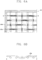
- FIGS. 6A and 6B are a plan view and a sectional view showing, for example, a different wire mesh type diffuser plate in the liquid crystal display device according to an embodiment of the present invention illustrated in FIG. 4 .
- a wire mesh 223a is fabricated according to a twill weave mesh method by using synthetic fiber such as transparent polyester, nylon, or the like, or stainless steel (SUS) as thread.
- synthetic fiber such as transparent polyester, nylon, or the like, or stainless steel (SUS) as thread.
- tension is provided to the wire mesh through traction of pulling the wire mesh several times until when the tension reaches predetermined tension.
- the weave mesh is a tissue forming a furrow pattern in a comb direction with warp and weft on a surface of fabric
- the wire mesh type diffuser plate 223 fabricated according to the twill weave mesh method has an increased contact area with the optical sheets compared with the plain weave mesh method as described above but has a smooth surface and thus it is more advantageous for preventing abrasion of the optical sheets.
- the wire mesh type diffuser plate 223 fabricated to have predetermined tension as described above advantageously does not require a fixing support for supporting the diffuser plate 223 and the optical sheets.
- an emulsion may be coated on the entire surface of the wire mesh type diffuser plate 223 or an emulsion may be coated on the outermost portion of the wire mesh type diffuser plate 223 to form the emulsion coated portion 223b.
- FIG. 7 is a flow chart illustrating a sequential fabrication process of the wire mesh type diffuser plate according to an embodiment of the present invention.
- FIG. 8 is a plan view illustrating, for example, a state that a plurality of unit wire mesh type diffuser plates are divided on a large base diffuser plate.
- a wire mesh is fabricated according to a plain weave mesh method by using synthetic fiber such as transparent polyester, nylon, or the like, or stainless steel as thread and tension is provided to the wire mesh through traction of pulling the wire mesh several times until when the tension reaches predetermined tension (S110).
- the wire mesh is a film type, it may be cut by inches to provide tension when fastened to the lower cover, and in this case, pressure applied to the wire mesh should be uniformly maintained.
- the plain weave mesh is the most basic tissue in which warp and weft are alternately crossed, and the wire mesh type diffuser plate fabricated according to the plain weave mesh method has a minimized contact area with the optical sheets of the backlight unit to prevent abrasion of the optical sheets, and reduce static electricity.
- the weave mesh is a tissue forming a furrow pattern in a comb direction with warp and weft on a surface of fabric
- the wire mesh type diffuser plate 223 fabricated according to the twill weave mesh method has an increased contact area with the optical sheets compared with the plain weave mesh method as described above but has a smooth surface and thus it is more advantageous for preventing abrasion of the optical sheets.
- the wire mesh type diffuser plate according to an embodiment of the present invention is fabricated in a state that unit a plurality of wire mesh type diffuser plates 123 are divided on a large base diffuser plate 120, and fabricated through emulsion coating and certain cutting process (See FIG. 8 ).
- an emulsion is coated to the outermost portion by a desired size, aged, and cut into a plurality of unit wire mesh type diffuser plates 123 (S130, S140, S150).
- the coated emulsion is required to have excellent water resistance, moisture resistance, solvent resistance, maintain mechanical rigidity, and have a short aging time after the emulsion is coated.
- a diazo-based emulsion may be used in case of fabricating a small size, and when the size is increased, a diazo dual cure-based emulsion may be used.
- diazo is a compound including nitrogen and having good reactivity.
- FIGS. 9A and 9B are schematic views showing an emulsion used in the wire mesh type diffuser plate according to an embodiment of the present invention.
- the diazo-based emulsion may be an emulsion in which polyvinyl alcohol (PVA) 151, polyvinyl acetate (PVAC) 152, and diazo 153 are mixed, and a solvent-resistant emulsion or a water-resistant emulsion may be obtained according to a ratio of each component.
- PVA polyvinyl alcohol
- PVAC polyvinyl acetate
- diazo 153 diazo-based emulsion
- a solvent-resistant emulsion or a water-resistant emulsion may be obtained according to a ratio of each component.
- a ratio between the PVAC 152 and the PVA 151 is about 6:4, and in the water-resistant emulsion, a ratio between the PVAC 152 and the PVA 151 is about 2:8.
- the PVA 151 is water-soluble and has a considerable solvent-resistance
- the PVAC 152 is solvent-soluable and has a considerable water-resistance.
- the diazo dual cure-based emulsion is an emulsion in which an acrylic monomer 154 is mixed to the PVA 151, the PVAC 152, and the diazo 153.
- the acrylic monomer 154 cross-bridges the respective components such that all the components are equal.
- the emulsion may be coated to have a thickness of 1.5 ⁇ 2 times the wire diameter of the wire mesh. This is because 50 ⁇ 70% of the thickness of the coated emulsion is evaporated during an aging process after the emulsion is coated.
- the wire diameter of the wire mesh may have a value of about 10 ⁇ m ⁇ 120 ⁇ m.
- Electrooptical characteristics of the wire mesh type diffuser plate according to an embodiment of the present invention fabricated as described above may be controlled by adjusting the opening and the wire diameter (thickness) d of the wire mesh. Also, the electrooptical characteristics of the wire mesh type diffuser plate may be controlled by adjusting transparency of the wire mesh material.
- FIGS. 10A and 10B are graphs showing, for example, luminance characteristics according to a viewing angle.
- FIG. 10A shows an example of luminance characteristics according to a viewing angle in the diffuser plate based on the existing extruding method
- FIG. 10B shows an example of luminance characteristics according to a viewing angle in the wire mesh type diffuser plate according to an embodiment of the present invention.
- wire mesh type diffuser plate according to an embodiment of the present invention has the same electrooptical characteristics as that of the diffuser plate based on the existing extruding method.
Landscapes
- Physics & Mathematics (AREA)
- General Physics & Mathematics (AREA)
- Optics & Photonics (AREA)
- Nonlinear Science (AREA)
- Mathematical Physics (AREA)
- Crystallography & Structural Chemistry (AREA)
- Chemical & Material Sciences (AREA)
- Engineering & Computer Science (AREA)
- Manufacturing & Machinery (AREA)
- Liquid Crystal (AREA)
- Optical Elements Other Than Lenses (AREA)
- Planar Illumination Modules (AREA)
- Devices For Indicating Variable Information By Combining Individual Elements (AREA)
Description
- The present disclosure relates to a wire mesh type diffuser plate and a liquid crystal display device having the same, and particularly, to a wire mesh type diffuser plate used in a direct type backlight unit, a method of fabricating the same, and a liquid crystal display device having the same.
- A liquid crystal display (LCD) device is a display device in which data signals according to image information are individually supplied to pixels arranged in a matrix form and light transmittance of the pixels is adjusted to display a desired image.
- Thus, the LCD device includes a liquid crystal panel in which pixels are arranged in a matrix form and a driving unit for driving the pixels.
- The liquid crystal panel includes a color filter substrate and an array substrate attached in a facing manner with a uniform cell gap maintained therebetween, and a liquid crystal layer formed in the cell gap between the color filter substrate and the array substrate.
- Here, a common electrode and a pixel electrode are formed on the liquid crystal panel formed by attaching the color filter substrate and the array substrate to apply an electric field to the liquid crystal layer.
- Thus, in a state in which a voltage is applied to the common electrode, when a voltage of a data signal applied to the pixel electrode is controlled, liquid crystal of the liquid crystal layer rotates by dielectric anisotropy according to an electric field between the common electrode and the pixel electrode, thereby displaying characters or images by transmitting or blocking light by pixels.
- Here, the LCD device is a light receiving device that does not emit light by itself. That is, because the LCD device displays an image by adjusting transmittance of light coming from the outside, it requires a backlight unit.
- A related art LCD device will be described in detail with reference to the accompanying drawings.
-
FIG. 1 illustrates a sectional view schematically showing a portion of a structure of a related art LCD device. - As illustrated, a related art LCD device includes a
liquid crystal panel 10 on which pixels are arranged in a matrix form to output an image, a driving unit (not shown) for driving the pixels, a backlight unit installed on a rear surface of theliquid crystal panel 10 to emit light to a front surface of theliquid crystal panel 10, and apanel guide 25 receiving theliquid crystal panel 10 and the backlight unit and fixing them. - Here, the
liquid crystal panel 10 includes acolor filter substrate 1 and an array substrate 11 attached in a facing manner with a uniform cell gap maintained therebetween, and a liquid crystal layer formed in the cell gap between thecolor filter substrate 1 and the array substrate 11. - Although not illustrated, a common electrode and a pixel electrode are formed on the
liquid crystal panel 10 formed by attaching thecolor filter substrate 1 and the array substrate 11 to apply an electric field to the liquid crystal layer. In a state in which a voltage is applied to the common electrode, when a voltage of a data signal applied to the pixel electrode is controlled, liquid crystal of the liquid crystal layer rotates by dielectric anisotropy according to an electric field between the common electrode and the pixel electrode, thereby displaying characters or images by transmitting or blocking light by pixels. - In order to control a voltage of a data signal applied to the pixel electrode by pixels, a switching element such as a thin film transistor (TFT) is individually provided in the pixels.
- Upper and lower polarization plates (not shown) are attached to an outer side of the liquid crystal panel. The lower polarization plate polarizes light passing through the backlight unit, and the upper polarization plate polarizes light passing through the
liquid crystal panel 10. - The backlight unit used as a light source of the liquid crystal panel is classified into an edge type backlight unit and a direct type backlight unit according to a method of disposing a light emitting lamp.
- In the direct type backlight unit, a
light emitting lamp 21 is disposed below theliquid crystal panel 10 to supply light. In detail, in the direct type backlight unit, a plurality oflamps 21 are disposed as light sources, and areflector 22 is positioned under the plurality oflamps 21. A plurality ofoptical sheets 24 are laminated and positioned above the plurality oflamps 21. - Here, because the direct type backlight unit does not use a light guide plate, a
diffuser plate 23 is provided between the plurality oflamps 21 and theoptical sheets 24 in order to diffuse light of the lamps and support theoptical sheets 24. - Also, although not illustrated, a conical fixing support is provided in order to support the
diffuser plate 23 and theoptical sheets 24 provided in the upper portion of thelamps 21. - The
liquid crystal panel 10 including thecolor filter substrate 1 and the array substrate 11 is mounted through thepanel guide 25 in an upper portion of the backlight unit configured as described above. Theliquid crystal panel 10, thepanel guide 25, and the backlight unit are coupled by alower cover bottom 30 and an upper case top 35 through a plurality offastening units - As a material of the
diffuser plate 23, polymethacryl styrene (MS), polystyrene (PS), polycarbonate (PC), or the like, is mainly used, and tolerance to thermal deformation and moisture and UV stability are required. -
FIG. 2 illustrates a sectional view showing a structure of a related art diffuser plate shown inFIG. 1 , for example. - As shown in the drawing, for example, an
existing diffuser plate 23 has a tri-layer structure in which plastic calledpolymetacryl styrene 23b is provided on both sides ofpolystyrene 23a provided in the middle portion. - The
diffuser plate 23 is fabricated through an extruding method. A polymer chip as a raw material is put in an extruder, discharged through a T-die, and then, passes through a roll so as to be fabricated. - The
diffuser plate 23 has a thickness of 1.2mm, 1.5mm, 2.0mm, or the like, and the thickness of thediffuser plate 23 is increased as an application inch of a liquid crystal panel is increased in order to secure reliability. - The fabricated
diffuser plate 23 is deformed due to moisture absorption, generating egg mura in the liquid crystal panel. -
FIGS. 3A and 3B illustrates sectional views showing a mechanism of generating egg mura. - With reference to these drawings, in the case of the direct type backlight unit, because the
lamp 21 as a light source exists below thediffuser plate 23, the lower side has a high temperature and theliquid crystal panel 10 side has a low temperature, so a temperature difference between the spaces generate moisture M. - Here, the
diffuser plate 23 absorbs the moisture M so as to be expanded toward theliquid crystal panel 10, and the expansion of thediffuser plate 23 lifts the surface of edges of theliquid crystal panel 10 to generate egg mura having an egg shape. Moisture M in a surrounding environment also makes the same influence. - That is, because the polarization plate, the
optical sheets 24, and thediffuser plate 23 absorb moisture M in a high temperature and high moisture environment, when the backlight unit is driven, theliquid crystal panel 10, theoptical sheets 24, and thediffuser plate 23 are warped. Here, a contact portion and a non-contact portion exist between the lower polarizer plate and theoptical sheets 24, and due to a different in moisture evaporation between the contact portion and the non-contact portion, the spots in the form of an egg mura are formed in theliquid crystal panel 10. - In order to improve this, the
diffuser plate 23 is required to have a predetermined thickness, which makes it difficult to implement a slim design. - Also, when the thickness of the
diffuser plate 23 is reduced, a resin flows down, non-molding, or the like, are generated in terms of the characteristics of the existing extruding process, having a limitation in reducing the thickness of thediffuser plate 23. That is, the thickness of thediffuser plate 23 is determined by passing a polishing roller during extruding, and in order to prevent a generation of non-molding, a predetermined thickness of thediffuser plate 23 should be maintained. -
WO 2007/046274 A1 discloses a backlight device for liquid crystal displays. The backlight device includes a light source, a textile as a diffuser plate and a frame which carries out spreading fixing of the textile. - Therefore, an aspect of the detailed description is to provide a wire mesh type diffuser plate improving egg mura generated in a direct type backlight unit, a method of fabricating the same, and a liquid crystal display device having the same.
- Other objects and features of the present invention will be described in the configuration and claims of the present invention hereinafter.
- To achieve these and other advantages and in accordance with the purpose of this specification, as embodied and broadly described herein, a liquid crystal display device includes: a liquid crystal panel displaying an image; a plurality of lamps installed below the liquid crystal panel and providing light to the liquid crystal panel; a plurality of optical sheets installed between the plurality of lamps and the liquid crystal panel; a reflection plate installed below the plurality of lamps; and a diffuser plate formed of a wire mesh having predetermined tension and installed between the plurality of lamps and the optical sheet and having predetermined tension.
- The wire mesh may use synthetic fiber such as transparent polyester, nylon, or the like, or stainless steel (SUS) as thread.
- The wire mesh may be formed through a plain weave mesh method or twill weave mesh method.
- The diffuser plate may form an emulsion coated portion by coating an emulsion on the entire surface thereof or coating an emulsion on the outermost portion thereof.
- Here, the emulsion may be a diazo-based emulsion or a diazo dual cure-based emulsion.
- The emulsion may be coated to have a thickness of 1.5 ∼ 2 times a wire diameter of a wire mesh.
- A wire diameter of the wire mesh has a value of about 10 µm - 120 µm.
- In the diffuser plate, a ratio of an opened region of the entire wire mesh may have a value of 30 ∼ 90%.
- A method of fabricating a wire mesh type diffuser plate includes: fabricating a wire mesh according to a plane weave mesh method or twill weave mesh method and providing tension through traction of pulling the wire mesh several times until when the tension reaches predetermined tension to fabricate a large base diffuser plate; measuring tension to inspect whether it has reached pre-set tension; coating an emulsion on the outermost portion of the traction-completed base diffuser plate by a desired size of a unit diffuser plate and drying it; and cutting the base diffuser plate into a plurality of unit diffuser plates.
- The wire mesh may use synthetic fiber such as transparent polyester, nylon, or the like, or stainless steel (SUS) as thread.
- Here, the emulsion may be a diazo-based emulsion or a diazo dual cure-based emulsion.
- The emulsion may be coated to have a thickness of 1.5 ∼ 2 times a wire diameter of a wire mesh.
- A wire diameter of the wire mesh may have a value of about 10 µm ∼ 120 µm.
- As described above, in the wire mesh type diffuser plate, the method of fabricating the same, and the liquid crystal display device having the same according to the present invention, a film type diffuser plate having predetermined tension is fabricated through traction by using a wire mesh instead of an existing diffuser plate based on an extruding method, and thus, egg mura generated in the direct type backlight unit can be improved.
- Thus, a thickness of the backlight unit can be reduced to contribute to making the display device slim and improvement of quality and a screen grade, and also, because cost for a raw material of the diffuser plate is reduced, fabrication cost of the liquid crystal display device can be reduced.
- Further scope of applicability of the present application will become more apparent from the detailed description given hereinafter. However, it should be understood that the detailed description and specific examples, while indicating preferred embodiments of the invention, are given by way of illustration only, since various changes and modifications within the spirit and scope of the invention will become apparent to those skilled in the art from the detailed description.
- The accompanying drawings, which are included to provide a further understanding of the invention and are incorporated in and constitute a part of this specification, illustrate exemplary embodiments and together with the description serve to explain the principles of the invention.
- In the drawings:
-
FIG. 1 illustrates a sectional view schematically showing a partial structure of a related art liquid crystal display device; -
FIG. 2 illustrates a sectional view showing a structure of a related art diffuser plate illustrated inFIG. 1 , for example; -
FIGS. 3A and 3B illustrate sectional views a mechanism of generating egg mura; -
FIG. 4 illustrates a sectional view schematically showing a partial structure of a liquid crystal display device according to an embodiment of the present invention; -
FIGS. 5A and 5B illustrate a plan view and a sectional view showing, for example, a wire mesh type diffuser plate in the liquid crystal display device according to an embodiment of the present invention illustrated inFIG. 4 ; -
FIGS. 6A and 6B are a plan view and a sectional view showing, for example, a different wire mesh type diffuser plate in the liquid crystal display device according to an embodiment of the present invention illustrated inFIG. 4 ; -
FIG. 7 is a flow chart illustrating a sequential fabrication process of the wire mesh type diffuser plate according to an embodiment of the present invention; -
FIG. 8 is a plan view illustrating, for example, a state that a plurality of unit wire mesh type diffuser plates are divided on a large base diffuser plate; -
FIGS. 9A and 9B are schematic views showing an emulsion used in the wire mesh type diffuser plate according to an embodiment of the present invention; and -
FIGS. 10A and 10B are graphs showing, for example, luminance characteristics according to a viewing angle. - Description will now be given in detail of the exemplary embodiments, with reference to the accompanying drawings. For the sake of brief description with reference to the drawings, the same or equivalent components will be provided with the same reference numbers, and description thereof will not be repeated.
- A wire mesh type diffuser plate, a method of fabricating the same, and a liquid crystal display device having the same according to embodiments of the present invention will be described in detail with reference to the accompanying drawings such that a person skilled in the art can easily implement the same. The present invention may be implemented in various forms and not limited to the embodiments described herein.
-
FIG. 4 illustrates a sectional view schematically showing a partial structure of a liquid crystal display device according to an embodiment of the present invention. - As illustrated in the drawing, the liquid crystal display (LCD) device according to an embodiment of the present invention includes a
liquid crystal panel 110 in which pixels are arranged in a matrix form to output an image, a driving unit (not shown) for driving the pixels, a backlight unit installed on a rear surface of theliquid crystal panel 110 to emit light to a front surface of theliquid crystal panel 110, and apanel guide 125 for receiving theliquid crystal panel 110 and the backlight unit and fixing them. - Here, the
liquid crystal panel 110 includes acolor filter substrate 101 and anarray substrate 111 attached in a facing manner with a uniform cell gap maintained therebetween, and a liquid crystal layer formed in the cell gap between thecolor filter substrate 101 and thearray substrate 111. - Here, although not shown in detail, the
color filter substrate 101 includes color filters including a plurality of sub-color filters implementing red, green, and blue colors, black matrices partitioning the sub-color filters and blocking light transmitted through the liquid crystal layer, and a transparent common electrode applying a voltage to the liquid crystal layer. - Also, the
array substrate 111 includes a plurality of gate lines and data lines arranged vertically and horizontally to define a plurality of pixel regions, thin film transistors as switching elements formed in intersections of the gate lines and data lines, and a pixel electrode formed on the pixel region. Here, in case of an in-plane switching (IPS) mode LCD device, a common electrode is formed on thearray substrate 111 instead of thecolor filter substrate 101. - A common electrode and a pixel electrode are formed on the
liquid crystal panel 110 in which thecolor filter substrate 101 and thearray substrate 111 are attached to apply an electric field to the liquid crystal layer, and when a voltage of a data signal applied to the pixel electrode in a state that a voltage is applied to the common electrode is controlled, liquid crystal of the liquid crystal layer is rotated by dielectric anisotropy according to the electric field between the common electrode and the data electrode, whereby light is transmitted or blocked by pixels to display a character or an image. - In order to control a voltage of the data signal applied to the pixel electrode by pixels, a switching element such as a thin film transistor is individually provided in the pixels.
- Upper and lower polarization plates (not shown) are attached to an outer side of the
liquid crystal panel 110, and the lower polarization plate polarizes light passing through the backlight unit and the upper polarization plate polarizes light passing through theliquid crystal panel 110. - Here, the upper and lower polarization plates are optical means for converting natural light or polarized light into linearly polarized light. The upper and lower polarization plates separate incident light into two polarization components perpendicular to each other, and allows one polarization component to be transmitted therethrough and absorbs, reflects and/or diffuses the other polarization component.
- A thickness of the upper and lower polarization plates is not particularly limited and includes a general concept of a thin film, a film, or a sheet.
- A direct type backlight unit according to an embodiment of the present invention will be described in detail. A plurality of
lamps 121 are disposed as lamps, and areflective plate 122 is positioned below the plurality oflamps 121. A plurality ofoptical sheets 124 are stacked and positioned above the plurality oflamps 121. - The
optical sheets 124 according to an embodiment of the present invention may include a diffusion sheet and a prism sheet, and may additionally include a protective sheet. - Here, because the direct type backlight unit does not use a light guide plate, a
diffuser plate 123 is provided between theplurality lamps 121 and theoptical sheet 124 in order to diffuse light of the lamps and support theoptical sheets 124. - The
liquid crystal panel 110 including thecolor filter substrate 101 and thearray substrate 111 is mounted on an upper portion of the backlight unit configured as described above through thepanel guide 125, and theliquid crystal panel 110, thepanel guide 125, and the backlight unit are combined with each other by alower cover bottom 130 and an upper case top 135 through a plurality offastening units - Here, the
diffuser plate 123 according to an embodiment of the present invention has characteristics that a film type diffuser plate using a wire mesh instead of a diffuser plate of an existing extruding method is applied. - The wire mesh
type diffuser plate 123 is fabricated as a film type having predetermined tension in order to cope with a change in a surrounding environment and dimensions when it is applied as a substitute of an existing diffuser plate. -
FIGS. 5A and 5B illustrate a plan view and a sectional view showing, for example, a wire mesh type diffuser plate in the liquid crystal display device according to an embodiment of the present invention illustrated inFIG. 4 . - With reference to these drawings, a
wire mesh 123a is fabricated by using synthetic fiber such as transparent polyester, nylon, or the like, or stainless steel (SUS) as thread according to a plain weave mesh method or twill weave mesh method. - Thereafter, tension is provided through traction of pulling the wire mesh several times until when the tension reaches predetermined tension.
- Here, the polyester fiber has strength second stronger than nylon when pulled, and its strength is not changed even when it is wet in water. Nylon is a general name of polyamide-based synthetic fiber, and it is thinner than a web and resistant to friction, and has excellent tensile strength relative to other fibers.
- The plane weave mesh is the most basic tissue in which warp and weft are alternately crossed, and the wire mesh
type diffuser plate 123 fabricated according to the plain weave mesh method has a minimized contact area with the optical sheets of the backlight unit to prevent abrasion of the optical sheets, and reduce static electricity. - The wire mesh
type diffuser plate 123 according to an embodiment of the present invention fabricated to have predetermined tension can improve egg mura generated in the direct type backlight unit, unlike the existing diffuser plate. Thus, a thickness of the backlight unit can be reduced to contribute to a slim display device and quality enhancement and screen grade enhancement, and because cost for a raw material of the diffuser plate is reduced, fabrication cost of the LCD device can be reduced. - Also, unlike the existing diffuser plate, a fixing support for supporting the wire mesh
type diffuser plate 123 and the optical sheets is not required. - Here, in order to maintain tension of the
wire mesh 123a and serve as a frame, an emulsion may be coated on the entire surface of the wire meshtype diffuser plate 123 or an emulsion may be coated on the outermost portion of the wire meshtype diffuser plate 123 to form an emulsion coatedportion 123b. - The emulsion coated
portion 123b is placed in edges of the reflective plate and supported between the reflective plate and the optical sheets, so tension can be maintained. - Electrooptical characteristics of the wire mesh
type diffuser plate 123 according to an embodiment of the present invention may be controlled by adjusting an opening w and a wire diameter (thickness) d of thewire mesh 123. Also, the electrooptical characteristics of the wire meshtype diffuser plate 123 may be controlled by adjusting transparency of a material forming thewire mesh 123a. - Here, an open area may be indicated as a rate (%) of the opened region in the
entire wire mesh 123a, and as the open area is reduced, transmittance is reduced, and as the open area is increased, transmittance is increased. - The open area of the
wire mesh 123a may have a value of about 30∼90%. - Meanwhile, the method for fabricating the wire mesh according to an embodiment of the present invention is not limited to the plain weave mesh method as described above, and the wire mesh may be fabricated according to a twill weave mesh method. This will be described in detail with reference to the following drawings.
-
FIGS. 6A and 6B are a plan view and a sectional view showing, for example, a different wire mesh type diffuser plate in the liquid crystal display device according to an embodiment of the present invention illustrated inFIG. 4 . - With reference to these drawings, a
wire mesh 223a is fabricated according to a twill weave mesh method by using synthetic fiber such as transparent polyester, nylon, or the like, or stainless steel (SUS) as thread. - Thereafter, tension is provided to the wire mesh through traction of pulling the wire mesh several times until when the tension reaches predetermined tension.
- The weave mesh is a tissue forming a furrow pattern in a comb direction with warp and weft on a surface of fabric, and the wire mesh
type diffuser plate 223 fabricated according to the twill weave mesh method has an increased contact area with the optical sheets compared with the plain weave mesh method as described above but has a smooth surface and thus it is more advantageous for preventing abrasion of the optical sheets. - Unlike the existing diffuser plate, the wire mesh
type diffuser plate 223 according to an embodiment of the present invention fabricated to have predetermined tension as described above advantageously does not require a fixing support for supporting thediffuser plate 223 and the optical sheets. - Here, in order to maintain the tension of the
wire mesh 223a and to make thewire mesh 223a serve as a frame, an emulsion may be coated on the entire surface of the wire meshtype diffuser plate 223 or an emulsion may be coated on the outermost portion of the wire meshtype diffuser plate 223 to form the emulsion coatedportion 223b. - A method for fabricating a wire mesh type diffuser plate according to an embodiment of the present invention configured as described above will be described in detail with reference to the accompanying drawings.
-
FIG. 7 is a flow chart illustrating a sequential fabrication process of the wire mesh type diffuser plate according to an embodiment of the present invention. - Also,
FIG. 8 is a plan view illustrating, for example, a state that a plurality of unit wire mesh type diffuser plates are divided on a large base diffuser plate. - First, a wire mesh is fabricated according to a plain weave mesh method by using synthetic fiber such as transparent polyester, nylon, or the like, or stainless steel as thread and tension is provided to the wire mesh through traction of pulling the wire mesh several times until when the tension reaches predetermined tension (S110).
- Here, since the wire mesh is a film type, it may be cut by inches to provide tension when fastened to the lower cover, and in this case, pressure applied to the wire mesh should be uniformly maintained.
- As described above, the plain weave mesh is the most basic tissue in which warp and weft are alternately crossed, and the wire mesh type diffuser plate fabricated according to the plain weave mesh method has a minimized contact area with the optical sheets of the backlight unit to prevent abrasion of the optical sheets, and reduce static electricity.
- Also, the weave mesh is a tissue forming a furrow pattern in a comb direction with warp and weft on a surface of fabric, and the wire mesh
type diffuser plate 223 fabricated according to the twill weave mesh method has an increased contact area with the optical sheets compared with the plain weave mesh method as described above but has a smooth surface and thus it is more advantageous for preventing abrasion of the optical sheets. - Thereafter, tension is measured and it is inspected whether it has reached pre-set tension (S120).
- Here, the wire mesh type diffuser plate according to an embodiment of the present invention is fabricated in a state that unit a plurality of wire mesh
type diffuser plates 123 are divided on a largebase diffuser plate 120, and fabricated through emulsion coating and certain cutting process (SeeFIG. 8 ). - That is, in order to fabricate the large
base diffuser plate 120 which has been completed for traction as a single product, an emulsion is coated to the outermost portion by a desired size, aged, and cut into a plurality of unit wire mesh type diffuser plates 123 (S130, S140, S150). - Here, in order to maintain tension of the wire mesh and serve as a frame, the coated emulsion is required to have excellent water resistance, moisture resistance, solvent resistance, maintain mechanical rigidity, and have a short aging time after the emulsion is coated.
- As the emulsion, a diazo-based emulsion may be used in case of fabricating a small size, and when the size is increased, a diazo dual cure-based emulsion may be used. Here, diazo is a compound including nitrogen and having good reactivity.
-
FIGS. 9A and 9B are schematic views showing an emulsion used in the wire mesh type diffuser plate according to an embodiment of the present invention. - Referring to
FIG. 9A , the diazo-based emulsion may be an emulsion in which polyvinyl alcohol (PVA) 151, polyvinyl acetate (PVAC) 152, anddiazo 153 are mixed, and a solvent-resistant emulsion or a water-resistant emulsion may be obtained according to a ratio of each component. - In the solvent-resistant emulsion, a ratio between the
PVAC 152 and thePVA 151 is about 6:4, and in the water-resistant emulsion, a ratio between thePVAC 152 and thePVA 151 is about 2:8. - The
PVA 151 is water-soluble and has a considerable solvent-resistance, and thePVAC 152 is solvent-soluable and has a considerable water-resistance. - Also, referring to
FIG. 9B , the diazo dual cure-based emulsion is an emulsion in which anacrylic monomer 154 is mixed to thePVA 151, thePVAC 152, and thediazo 153. - The
acrylic monomer 154 cross-bridges the respective components such that all the components are equal. - The emulsion may be coated to have a thickness of 1.5 ∼ 2 times the wire diameter of the wire mesh. This is because 50∼70% of the thickness of the coated emulsion is evaporated during an aging process after the emulsion is coated.
- Here, the wire diameter of the wire mesh may have a value of about 10 µm ∼120 µm.
- Electrooptical characteristics of the wire mesh type diffuser plate according to an embodiment of the present invention fabricated as described above may be controlled by adjusting the opening and the wire diameter (thickness) d of the wire mesh. Also, the electrooptical characteristics of the wire mesh type diffuser plate may be controlled by adjusting transparency of the wire mesh material.
-
FIGS. 10A and 10B are graphs showing, for example, luminance characteristics according to a viewing angle. - Here,
FIG. 10A shows an example of luminance characteristics according to a viewing angle in the diffuser plate based on the existing extruding method, andFIG. 10B shows an example of luminance characteristics according to a viewing angle in the wire mesh type diffuser plate according to an embodiment of the present invention. - With reference to the drawings, It is noted that even the wire mesh type diffuser plate according to an embodiment of the present invention has the same electrooptical characteristics as that of the diffuser plate based on the existing extruding method.
- The foregoing embodiments and advantages are merely exemplary and are not to be considered as limiting the present disclosure. The present teachings can be readily applied to other types of apparatuses. This description is intended to be illustrative, and not to limit the scope of the claims. Many alternatives, modifications, and variations will be apparent to those skilled in the art. The features, structures, methods, and other characteristics of the exemplary embodiments described herein may be combined in various ways to obtain additional and/or alternative exemplary embodiments.
- As the present features may be embodied in several forms without departing from the characteristics thereof, it should also be understood that the above-described embodiments are not limited by any of the details of the foregoing description, unless otherwise specified, but rather should be considered broadly within its scope as defined in the appended claims, and therefore all changes and modifications that fall within the metes and bounds of the claims, or equivalents of such metes and bounds are therefore intended to be embraced by the appended claims.
Claims (10)
- A liquid crystal display device comprising:a liquid crystal panel (110) displaying an image;a plurality of lamps (121) installed below the liquid crystal panel (110) and providing light to the liquid crystal panel (110);a plurality of optical sheets (124) installed between the plurality of lamps (121) and the liquid crystal panel (110);a reflection plate (122) installed below the plurality of lamps (121); anda diffuser plate (123) formed of a wire mesh (123a) having predetermined tension and installed between the plurality of lamps (121) and the optical sheet (124), characterized in that the entire surface or outermost portion of the diffuser plate comprises an aged emulsion coated portion (123b), andwherein the emulsion is a diazo-based emulsion or a diazo dual cure-based emulsion.
- The liquid crystal display device of claim 1, wherein the wire mesh (123a) uses synthetic fiber such as transparent polyester, nylon, or the like, or stainless steel (SUS) as thread.
- The liquid crystal display device of claim 1, wherein the wire mesh (123a) is formed through a plain weave mesh method or twill weave mesh method.
- The liquid crystal display device of claim 1, wherein the emulsion is coated to have a thickness of 1.5 ∼ 2 times a wire diameter of a wire mesh (123a).
- The liquid crystal display device of claim 4, wherein a wire diameter of the wire mesh (123a) has a value of about 10 µm ∼ 120 µm.
- The liquid crystal display device of claim 1, wherein in the diffuser plate (123), a ratio of an opened region of the entire wire mesh (123a) has a value of 30 ∼ 90%.
- A method of fabricating a wire mesh type diffuser plate (123), the method comprising:fabricating (S110) a wire mesh (123a) according to a plain weave mesh method or twill weave mesh method and providing tension through traction of pulling the wire mesh several times to fabricate a large base diffuser plate (120);measuring (S120) tension to inspect whether it has reached pre-set tension;coating (S130) an emulsion on the entire surface or outermost portion of the traction-completed base diffuser plate (120) by a desired size of a unit diffuser plate (123) and drying it, wherein the emulsion is a diazo-based emulsion or a diazo dual cure-based emulsion; andcutting (S150) the base diffuser plate (120) into a plurality of unit diffuser plates (123).
- The method of claim 7, wherein the wire mesh (123a) uses synthetic fiber such as transparent polyester, nylon, or the like, or stainless steel (SUS) as thread.
- The method of claim 7, wherein the emulsion is coated to have a thickness of 1.5 ∼ 2 times a wire diameter of a wire mesh (123a).
- The method of claim 7, wherein a wire diameter of the wire mesh (123a) has a value of about 10 µm ∼ 120 µm.
Applications Claiming Priority (1)
| Application Number | Priority Date | Filing Date | Title |
|---|---|---|---|
| KR1020120117480A KR102081158B1 (en) | 2012-10-22 | 2012-10-22 | Wire mesh type diffuser plate and method of fabricating the same, and liquid crystal display device having the wire mesh type diffuser plate |
Publications (3)
| Publication Number | Publication Date |
|---|---|
| EP2722708A2 EP2722708A2 (en) | 2014-04-23 |
| EP2722708A3 EP2722708A3 (en) | 2014-08-06 |
| EP2722708B1 true EP2722708B1 (en) | 2017-07-12 |
Family
ID=47561121
Family Applications (1)
| Application Number | Title | Priority Date | Filing Date |
|---|---|---|---|
| EP12197007.3A Active EP2722708B1 (en) | 2012-10-22 | 2012-12-13 | Wire mesh type diffuser plate and method of fabricating the same, and liquid crystal display device having the wire mesh type diffuser plate |
Country Status (5)
| Country | Link |
|---|---|
| US (1) | US9298031B2 (en) |
| EP (1) | EP2722708B1 (en) |
| JP (1) | JP5572687B2 (en) |
| KR (1) | KR102081158B1 (en) |
| CN (1) | CN103777401B (en) |
Families Citing this family (8)
| Publication number | Priority date | Publication date | Assignee | Title |
|---|---|---|---|---|
| CN104197245B (en) * | 2014-09-09 | 2017-06-16 | 深圳市华星光电技术有限公司 | Backlight module |
| DE102015106708B4 (en) * | 2015-04-30 | 2017-12-21 | Visteon Global Technologies, Inc. | Device for emitting light, in particular for generating an image |
| KR102621126B1 (en) * | 2015-12-30 | 2024-01-03 | 엘지디스플레이 주식회사 | Liquid crystal display device |
| DE102017215369A1 (en) * | 2017-09-01 | 2019-03-07 | Benecke-Kaliko Ag | Translucent multi-layer composite film |
| CN108572483B (en) * | 2018-04-26 | 2020-07-28 | 惠州市华星光电技术有限公司 | Direct type backlight module and liquid crystal display device |
| JP7293024B2 (en) | 2019-07-26 | 2023-06-19 | 東芝キヤリア株式会社 | Rotary compressor and refrigeration cycle equipment |
| KR102633932B1 (en) * | 2019-08-05 | 2024-02-05 | 엘지디스플레이 주식회사 | Diffusion mesh film, backlight unit and display device |
| CN113671753B (en) * | 2021-08-19 | 2023-06-09 | 福州京东方光电科技有限公司 | Backlight module and display device |
Family Cites Families (15)
| Publication number | Priority date | Publication date | Assignee | Title |
|---|---|---|---|---|
| JPS5936837B2 (en) * | 1977-04-05 | 1984-09-06 | 株式会社東芝 | Optical semiconductor device |
| JPH06102506A (en) | 1992-09-04 | 1994-04-15 | Minnesota Mining & Mfg Co <3M> | Display device |
| US5411628A (en) * | 1993-10-21 | 1995-05-02 | E. I. Du Pont De Nemours And Company | Diffusion patterning process and screen therefor |
| JP4132546B2 (en) * | 2000-02-29 | 2008-08-13 | 富士フイルム株式会社 | Light diffusing plate, method for manufacturing light diffusing plate, and display device |
| JP2005201938A (en) * | 2004-01-13 | 2005-07-28 | Mitsubishi Rayon Co Ltd | Liquid crystal display |
| JPWO2005116518A1 (en) | 2004-05-26 | 2008-04-03 | 多摩ファインオプト株式会社 | Liquid crystal display device and backlight device |
| JP2006018104A (en) | 2004-07-02 | 2006-01-19 | Dainippon Printing Co Ltd | Optically functional film and display provided with the same |
| JP2006312658A (en) | 2005-05-06 | 2006-11-16 | Mitsubishi Rayon Co Ltd | Acrylic resin composition, acrylic resin molded product composed of the same acrylic resin composition and light diffusing plate |
| KR20060124831A (en) * | 2005-05-26 | 2006-12-06 | 엘지이노텍 주식회사 | Backlight assembly and lcd having the same |
| WO2007046274A1 (en) * | 2005-10-18 | 2007-04-26 | Toray Industries, Inc. | Optical sheet-supporting body, backlight for liquid crystal display using same, and liquid crystal display |
| KR100908184B1 (en) | 2006-07-31 | 2009-07-16 | 주식회사 엘지화학 | Polarizing plate and liquid crystal display device using same |
| DE102006048473A1 (en) * | 2006-10-11 | 2008-04-17 | Sefar Ag | Rear projection fabric, rear projection screen and rear projection system |
| JP5412287B2 (en) | 2007-09-26 | 2014-02-12 | 株式会社きもと | Light diffusing film and light source device using the same |
| CN102449381A (en) * | 2009-06-15 | 2012-05-09 | 夏普株式会社 | Light-source unit, lighting device, displaying device, television-receiver device, and manufacturing method of reflection-sheets for light-sources |
| TW201224334A (en) * | 2010-12-07 | 2012-06-16 | Ind Tech Res Inst | Flexible light source module |
-
2012
- 2012-10-22 KR KR1020120117480A patent/KR102081158B1/en active IP Right Grant
- 2012-12-13 EP EP12197007.3A patent/EP2722708B1/en active Active
- 2012-12-26 US US13/726,939 patent/US9298031B2/en active Active
- 2012-12-28 JP JP2012286540A patent/JP5572687B2/en not_active Expired - Fee Related
- 2012-12-28 CN CN201210599233.9A patent/CN103777401B/en active Active
Non-Patent Citations (1)
| Title |
|---|
| None * |
Also Published As
| Publication number | Publication date |
|---|---|
| JP2014085662A (en) | 2014-05-12 |
| US20140111742A1 (en) | 2014-04-24 |
| EP2722708A2 (en) | 2014-04-23 |
| CN103777401A (en) | 2014-05-07 |
| JP5572687B2 (en) | 2014-08-13 |
| US9298031B2 (en) | 2016-03-29 |
| CN103777401B (en) | 2016-08-24 |
| EP2722708A3 (en) | 2014-08-06 |
| KR20140050988A (en) | 2014-04-30 |
| KR102081158B1 (en) | 2020-02-25 |
Similar Documents
| Publication | Publication Date | Title |
|---|---|---|
| EP2722708B1 (en) | Wire mesh type diffuser plate and method of fabricating the same, and liquid crystal display device having the wire mesh type diffuser plate | |
| US9366893B2 (en) | Liquid crystal display device | |
| US9377652B2 (en) | Liquid crystal display device | |
| CN101769476A (en) | Backlight unit and liquid crystal display module including the same | |
| GB2455396A (en) | Liquid crystal display module including light-blocking tape to overcome light leakage caused by support unit | |
| US7859612B2 (en) | Light concentrating sheet, backlight unit including the light concentrating sheet and liquid crystal display module including the backlight unit | |
| KR20140052819A (en) | Liquid crystal display device having backlight unit to be able to control viewing angle | |
| KR20100075134A (en) | Backlight unit for liquid crystal display device | |
| CN104698518A (en) | Prismatic lens, backlight module adopting prismatic lens and liquid crystal display | |
| CN107884985B (en) | Liquid crystal display device having a plurality of pixel electrodes | |
| US8052319B2 (en) | Diffusion plate and display apparatus having the same | |
| KR20110103729A (en) | Display apparatus | |
| KR101282289B1 (en) | Lamp guide and backlight unit for LCD including the same | |
| KR101047601B1 (en) | Backlight unit and display device using same | |
| KR20110018233A (en) | Liquid crystal display device | |
| KR100880217B1 (en) | A Back light | |
| US20100165248A1 (en) | Backlight unit and liquid crystal display device having the same | |
| KR101746679B1 (en) | Optical fiber array sheet and LCD including the same | |
| KR20100028458A (en) | Light guide plate and backlight unit for liquid crystal display device using the same | |
| KR101688991B1 (en) | Reflect Sheet and Backlight Unit having the Same | |
| KR20090053000A (en) | Backlight assembly for flexible lcd | |
| KR102135918B1 (en) | Liquid crystal display device having backlight unit to be able to control viewing angle | |
| KR20130028270A (en) | Reflecting sheet and method for manufacturing the same, liquid crystal display device including reflecting sheet | |
| KR20060112370A (en) | Liquid crystal display device module | |
| KR101392486B1 (en) | Liquid crystal dispaly device |
Legal Events
| Date | Code | Title | Description |
|---|---|---|---|
| PUAI | Public reference made under article 153(3) epc to a published international application that has entered the european phase |
Free format text: ORIGINAL CODE: 0009012 |
|
| AK | Designated contracting states |
Kind code of ref document: A2 Designated state(s): AL AT BE BG CH CY CZ DE DK EE ES FI FR GB GR HR HU IE IS IT LI LT LU LV MC MK MT NL NO PL PT RO RS SE SI SK SM TR |
|
| AX | Request for extension of the european patent |
Extension state: BA ME |
|
| 17P | Request for examination filed |
Effective date: 20140328 |
|
| RBV | Designated contracting states (corrected) |
Designated state(s): AL AT BE BG CH CY CZ DE DK EE ES FI FR GB GR HR HU IE IS IT LI LT LU LV MC MK MT NL NO PL PT RO RS SE SI SK SM TR |
|
| PUAL | Search report despatched |
Free format text: ORIGINAL CODE: 0009013 |
|
| AK | Designated contracting states |
Kind code of ref document: A3 Designated state(s): AL AT BE BG CH CY CZ DE DK EE ES FI FR GB GR HR HU IE IS IT LI LT LU LV MC MK MT NL NO PL PT RO RS SE SI SK SM TR |
|
| AX | Request for extension of the european patent |
Extension state: BA ME |
|
| RIC1 | Information provided on ipc code assigned before grant |
Ipc: G02F 1/1335 20060101AFI20140629BHEP Ipc: G02F 1/13357 20060101ALI20140629BHEP Ipc: G02B 5/02 20060101ALI20140629BHEP |
|
| GRAP | Despatch of communication of intention to grant a patent |
Free format text: ORIGINAL CODE: EPIDOSNIGR1 |
|
| INTG | Intention to grant announced |
Effective date: 20170117 |
|
| GRAS | Grant fee paid |
Free format text: ORIGINAL CODE: EPIDOSNIGR3 |
|
| GRAJ | Information related to disapproval of communication of intention to grant by the applicant or resumption of examination proceedings by the epo deleted |
Free format text: ORIGINAL CODE: EPIDOSDIGR1 |
|
| GRAL | Information related to payment of fee for publishing/printing deleted |
Free format text: ORIGINAL CODE: EPIDOSDIGR3 |
|
| GRAR | Information related to intention to grant a patent recorded |
Free format text: ORIGINAL CODE: EPIDOSNIGR71 |
|
| GRAA | (expected) grant |
Free format text: ORIGINAL CODE: 0009210 |
|
| INTC | Intention to grant announced (deleted) | ||
| AK | Designated contracting states |
Kind code of ref document: B1 Designated state(s): AL AT BE BG CH CY CZ DE DK EE ES FI FR GB GR HR HU IE IS IT LI LT LU LV MC MK MT NL NO PL PT RO RS SE SI SK SM TR |
|
| INTG | Intention to grant announced |
Effective date: 20170606 |
|
| REG | Reference to a national code |
Ref country code: GB Ref legal event code: FG4D |
|
| REG | Reference to a national code |
Ref country code: CH Ref legal event code: EP |
|
| REG | Reference to a national code |
Ref country code: AT Ref legal event code: REF Ref document number: 908890 Country of ref document: AT Kind code of ref document: T Effective date: 20170715 |
|
| REG | Reference to a national code |
Ref country code: IE Ref legal event code: FG4D |
|
| REG | Reference to a national code |
Ref country code: DE Ref legal event code: R096 Ref document number: 602012034375 Country of ref document: DE |
|
| REG | Reference to a national code |
Ref country code: NL Ref legal event code: MP Effective date: 20170712 |
|
| REG | Reference to a national code |
Ref country code: LT Ref legal event code: MG4D |
|
| REG | Reference to a national code |
Ref country code: AT Ref legal event code: MK05 Ref document number: 908890 Country of ref document: AT Kind code of ref document: T Effective date: 20170712 |
|
| PG25 | Lapsed in a contracting state [announced via postgrant information from national office to epo] |
Ref country code: NL Free format text: LAPSE BECAUSE OF FAILURE TO SUBMIT A TRANSLATION OF THE DESCRIPTION OR TO PAY THE FEE WITHIN THE PRESCRIBED TIME-LIMIT Effective date: 20170712 Ref country code: FI Free format text: LAPSE BECAUSE OF FAILURE TO SUBMIT A TRANSLATION OF THE DESCRIPTION OR TO PAY THE FEE WITHIN THE PRESCRIBED TIME-LIMIT Effective date: 20170712 Ref country code: LT Free format text: LAPSE BECAUSE OF FAILURE TO SUBMIT A TRANSLATION OF THE DESCRIPTION OR TO PAY THE FEE WITHIN THE PRESCRIBED TIME-LIMIT Effective date: 20170712 Ref country code: NO Free format text: LAPSE BECAUSE OF FAILURE TO SUBMIT A TRANSLATION OF THE DESCRIPTION OR TO PAY THE FEE WITHIN THE PRESCRIBED TIME-LIMIT Effective date: 20171012 Ref country code: SE Free format text: LAPSE BECAUSE OF FAILURE TO SUBMIT A TRANSLATION OF THE DESCRIPTION OR TO PAY THE FEE WITHIN THE PRESCRIBED TIME-LIMIT Effective date: 20170712 Ref country code: AT Free format text: LAPSE BECAUSE OF FAILURE TO SUBMIT A TRANSLATION OF THE DESCRIPTION OR TO PAY THE FEE WITHIN THE PRESCRIBED TIME-LIMIT Effective date: 20170712 Ref country code: HR Free format text: LAPSE BECAUSE OF FAILURE TO SUBMIT A TRANSLATION OF THE DESCRIPTION OR TO PAY THE FEE WITHIN THE PRESCRIBED TIME-LIMIT Effective date: 20170712 |
|
| PG25 | Lapsed in a contracting state [announced via postgrant information from national office to epo] |
Ref country code: RS Free format text: LAPSE BECAUSE OF FAILURE TO SUBMIT A TRANSLATION OF THE DESCRIPTION OR TO PAY THE FEE WITHIN THE PRESCRIBED TIME-LIMIT Effective date: 20170712 Ref country code: ES Free format text: LAPSE BECAUSE OF FAILURE TO SUBMIT A TRANSLATION OF THE DESCRIPTION OR TO PAY THE FEE WITHIN THE PRESCRIBED TIME-LIMIT Effective date: 20170712 Ref country code: IS Free format text: LAPSE BECAUSE OF FAILURE TO SUBMIT A TRANSLATION OF THE DESCRIPTION OR TO PAY THE FEE WITHIN THE PRESCRIBED TIME-LIMIT Effective date: 20171112 Ref country code: PL Free format text: LAPSE BECAUSE OF FAILURE TO SUBMIT A TRANSLATION OF THE DESCRIPTION OR TO PAY THE FEE WITHIN THE PRESCRIBED TIME-LIMIT Effective date: 20170712 Ref country code: LV Free format text: LAPSE BECAUSE OF FAILURE TO SUBMIT A TRANSLATION OF THE DESCRIPTION OR TO PAY THE FEE WITHIN THE PRESCRIBED TIME-LIMIT Effective date: 20170712 Ref country code: GR Free format text: LAPSE BECAUSE OF FAILURE TO SUBMIT A TRANSLATION OF THE DESCRIPTION OR TO PAY THE FEE WITHIN THE PRESCRIBED TIME-LIMIT Effective date: 20171013 Ref country code: BG Free format text: LAPSE BECAUSE OF FAILURE TO SUBMIT A TRANSLATION OF THE DESCRIPTION OR TO PAY THE FEE WITHIN THE PRESCRIBED TIME-LIMIT Effective date: 20171012 |
|
| REG | Reference to a national code |
Ref country code: DE Ref legal event code: R097 Ref document number: 602012034375 Country of ref document: DE |
|
| PG25 | Lapsed in a contracting state [announced via postgrant information from national office to epo] |
Ref country code: CZ Free format text: LAPSE BECAUSE OF FAILURE TO SUBMIT A TRANSLATION OF THE DESCRIPTION OR TO PAY THE FEE WITHIN THE PRESCRIBED TIME-LIMIT Effective date: 20170712 Ref country code: DK Free format text: LAPSE BECAUSE OF FAILURE TO SUBMIT A TRANSLATION OF THE DESCRIPTION OR TO PAY THE FEE WITHIN THE PRESCRIBED TIME-LIMIT Effective date: 20170712 Ref country code: RO Free format text: LAPSE BECAUSE OF FAILURE TO SUBMIT A TRANSLATION OF THE DESCRIPTION OR TO PAY THE FEE WITHIN THE PRESCRIBED TIME-LIMIT Effective date: 20170712 |
|
| PLBE | No opposition filed within time limit |
Free format text: ORIGINAL CODE: 0009261 |
|
| STAA | Information on the status of an ep patent application or granted ep patent |
Free format text: STATUS: NO OPPOSITION FILED WITHIN TIME LIMIT |
|
| PG25 | Lapsed in a contracting state [announced via postgrant information from national office to epo] |
Ref country code: SM Free format text: LAPSE BECAUSE OF FAILURE TO SUBMIT A TRANSLATION OF THE DESCRIPTION OR TO PAY THE FEE WITHIN THE PRESCRIBED TIME-LIMIT Effective date: 20170712 Ref country code: IT Free format text: LAPSE BECAUSE OF FAILURE TO SUBMIT A TRANSLATION OF THE DESCRIPTION OR TO PAY THE FEE WITHIN THE PRESCRIBED TIME-LIMIT Effective date: 20170712 Ref country code: EE Free format text: LAPSE BECAUSE OF FAILURE TO SUBMIT A TRANSLATION OF THE DESCRIPTION OR TO PAY THE FEE WITHIN THE PRESCRIBED TIME-LIMIT Effective date: 20170712 Ref country code: SK Free format text: LAPSE BECAUSE OF FAILURE TO SUBMIT A TRANSLATION OF THE DESCRIPTION OR TO PAY THE FEE WITHIN THE PRESCRIBED TIME-LIMIT Effective date: 20170712 |
|
| 26N | No opposition filed |
Effective date: 20180413 |
|
| REG | Reference to a national code |
Ref country code: CH Ref legal event code: PL |
|
| PG25 | Lapsed in a contracting state [announced via postgrant information from national office to epo] |
Ref country code: SI Free format text: LAPSE BECAUSE OF FAILURE TO SUBMIT A TRANSLATION OF THE DESCRIPTION OR TO PAY THE FEE WITHIN THE PRESCRIBED TIME-LIMIT Effective date: 20170712 |
|
| REG | Reference to a national code |
Ref country code: IE Ref legal event code: MM4A |
|
| PG25 | Lapsed in a contracting state [announced via postgrant information from national office to epo] |
Ref country code: MT Free format text: LAPSE BECAUSE OF NON-PAYMENT OF DUE FEES Effective date: 20171213 Ref country code: LU Free format text: LAPSE BECAUSE OF NON-PAYMENT OF DUE FEES Effective date: 20171213 |
|
| REG | Reference to a national code |
Ref country code: FR Ref legal event code: ST Effective date: 20180831 |
|
| REG | Reference to a national code |
Ref country code: BE Ref legal event code: MM Effective date: 20171231 |
|
| PG25 | Lapsed in a contracting state [announced via postgrant information from national office to epo] |
Ref country code: FR Free format text: LAPSE BECAUSE OF NON-PAYMENT OF DUE FEES Effective date: 20180102 Ref country code: IE Free format text: LAPSE BECAUSE OF NON-PAYMENT OF DUE FEES Effective date: 20171213 |
|
| PG25 | Lapsed in a contracting state [announced via postgrant information from national office to epo] |
Ref country code: CH Free format text: LAPSE BECAUSE OF NON-PAYMENT OF DUE FEES Effective date: 20171231 Ref country code: BE Free format text: LAPSE BECAUSE OF NON-PAYMENT OF DUE FEES Effective date: 20171231 Ref country code: LI Free format text: LAPSE BECAUSE OF NON-PAYMENT OF DUE FEES Effective date: 20171231 |
|
| PG25 | Lapsed in a contracting state [announced via postgrant information from national office to epo] |
Ref country code: MC Free format text: LAPSE BECAUSE OF FAILURE TO SUBMIT A TRANSLATION OF THE DESCRIPTION OR TO PAY THE FEE WITHIN THE PRESCRIBED TIME-LIMIT Effective date: 20170712 Ref country code: HU Free format text: LAPSE BECAUSE OF FAILURE TO SUBMIT A TRANSLATION OF THE DESCRIPTION OR TO PAY THE FEE WITHIN THE PRESCRIBED TIME-LIMIT; INVALID AB INITIO Effective date: 20121213 |
|
| PG25 | Lapsed in a contracting state [announced via postgrant information from national office to epo] |
Ref country code: CY Free format text: LAPSE BECAUSE OF NON-PAYMENT OF DUE FEES Effective date: 20170712 |
|
| PG25 | Lapsed in a contracting state [announced via postgrant information from national office to epo] |
Ref country code: MK Free format text: LAPSE BECAUSE OF FAILURE TO SUBMIT A TRANSLATION OF THE DESCRIPTION OR TO PAY THE FEE WITHIN THE PRESCRIBED TIME-LIMIT Effective date: 20170712 |
|
| PG25 | Lapsed in a contracting state [announced via postgrant information from national office to epo] |
Ref country code: TR Free format text: LAPSE BECAUSE OF FAILURE TO SUBMIT A TRANSLATION OF THE DESCRIPTION OR TO PAY THE FEE WITHIN THE PRESCRIBED TIME-LIMIT Effective date: 20170712 |
|
| PG25 | Lapsed in a contracting state [announced via postgrant information from national office to epo] |
Ref country code: PT Free format text: LAPSE BECAUSE OF FAILURE TO SUBMIT A TRANSLATION OF THE DESCRIPTION OR TO PAY THE FEE WITHIN THE PRESCRIBED TIME-LIMIT Effective date: 20170712 |
|
| PG25 | Lapsed in a contracting state [announced via postgrant information from national office to epo] |
Ref country code: AL Free format text: LAPSE BECAUSE OF FAILURE TO SUBMIT A TRANSLATION OF THE DESCRIPTION OR TO PAY THE FEE WITHIN THE PRESCRIBED TIME-LIMIT Effective date: 20170712 |
|
| PGFP | Annual fee paid to national office [announced via postgrant information from national office to epo] |
Ref country code: GB Payment date: 20231023 Year of fee payment: 12 |
|
| PGFP | Annual fee paid to national office [announced via postgrant information from national office to epo] |
Ref country code: DE Payment date: 20231023 Year of fee payment: 12 |