EP2722192A1 - Identity card with a physical unclonable function - Google Patents
Identity card with a physical unclonable function Download PDFInfo
- Publication number
- EP2722192A1 EP2722192A1 EP20120188964 EP12188964A EP2722192A1 EP 2722192 A1 EP2722192 A1 EP 2722192A1 EP 20120188964 EP20120188964 EP 20120188964 EP 12188964 A EP12188964 A EP 12188964A EP 2722192 A1 EP2722192 A1 EP 2722192A1
- Authority
- EP
- European Patent Office
- Prior art keywords
- light reflecting
- reflecting elements
- arrangement
- light
- card body
- Prior art date
- Legal status (The legal status is an assumption and is not a legal conclusion. Google has not performed a legal analysis and makes no representation as to the accuracy of the status listed.)
- Granted
Links
Images


Classifications
-
- G—PHYSICS
- G06—COMPUTING OR CALCULATING; COUNTING
- G06V—IMAGE OR VIDEO RECOGNITION OR UNDERSTANDING
- G06V20/00—Scenes; Scene-specific elements
- G06V20/80—Recognising image objects characterised by unique random patterns
-
- B—PERFORMING OPERATIONS; TRANSPORTING
- B42—BOOKBINDING; ALBUMS; FILES; SPECIAL PRINTED MATTER
- B42D—BOOKS; BOOK COVERS; LOOSE LEAVES; PRINTED MATTER CHARACTERISED BY IDENTIFICATION OR SECURITY FEATURES; PRINTED MATTER OF SPECIAL FORMAT OR STYLE NOT OTHERWISE PROVIDED FOR; DEVICES FOR USE THEREWITH AND NOT OTHERWISE PROVIDED FOR; MOVABLE-STRIP WRITING OR READING APPARATUS
- B42D25/00—Information-bearing cards or sheet-like structures characterised by identification or security features; Manufacture thereof
- B42D25/20—Information-bearing cards or sheet-like structures characterised by identification or security features; Manufacture thereof characterised by a particular use or purpose
- B42D25/23—Identity cards
-
- B—PERFORMING OPERATIONS; TRANSPORTING
- B42—BOOKBINDING; ALBUMS; FILES; SPECIAL PRINTED MATTER
- B42D—BOOKS; BOOK COVERS; LOOSE LEAVES; PRINTED MATTER CHARACTERISED BY IDENTIFICATION OR SECURITY FEATURES; PRINTED MATTER OF SPECIAL FORMAT OR STYLE NOT OTHERWISE PROVIDED FOR; DEVICES FOR USE THEREWITH AND NOT OTHERWISE PROVIDED FOR; MOVABLE-STRIP WRITING OR READING APPARATUS
- B42D25/00—Information-bearing cards or sheet-like structures characterised by identification or security features; Manufacture thereof
- B42D25/20—Information-bearing cards or sheet-like structures characterised by identification or security features; Manufacture thereof characterised by a particular use or purpose
- B42D25/29—Securities; Bank notes
-
- G—PHYSICS
- G06—COMPUTING OR CALCULATING; COUNTING
- G06V—IMAGE OR VIDEO RECOGNITION OR UNDERSTANDING
- G06V10/00—Arrangements for image or video recognition or understanding
- G06V10/10—Image acquisition
- G06V10/12—Details of acquisition arrangements; Constructional details thereof
- G06V10/14—Optical characteristics of the device performing the acquisition or on the illumination arrangements
- G06V10/147—Details of sensors, e.g. sensor lenses
-
- B42D2033/10—
-
- B42D2033/18—
-
- B42D2035/16—
-
- B—PERFORMING OPERATIONS; TRANSPORTING
- B42—BOOKBINDING; ALBUMS; FILES; SPECIAL PRINTED MATTER
- B42D—BOOKS; BOOK COVERS; LOOSE LEAVES; PRINTED MATTER CHARACTERISED BY IDENTIFICATION OR SECURITY FEATURES; PRINTED MATTER OF SPECIAL FORMAT OR STYLE NOT OTHERWISE PROVIDED FOR; DEVICES FOR USE THEREWITH AND NOT OTHERWISE PROVIDED FOR; MOVABLE-STRIP WRITING OR READING APPARATUS
- B42D25/00—Information-bearing cards or sheet-like structures characterised by identification or security features; Manufacture thereof
- B42D25/30—Identification or security features, e.g. for preventing forgery
- B42D25/328—Diffraction gratings; Holograms
Definitions
- the preset invention relates to identity cards with physical unclonable functions (PUF).
- PUFs Physical Unclonable Functions
- PUFs are functions embodied in physical structures which are easy to evaluate but hard to predict. Furthermore, implementations are difficult to duplicate, even if the exact manufacturing process is known and available. Consequently, security architectures based on PUFs promise inherent unclonability, physical tamper resistance and secure establishment of device-unique cryptographic keys.
- Well-known bare silicon PUFs aim at ensuring the security of the circuit itself but do not grant tamper resistance to the card in which it is embedded.
- the challenge-response behaviour of a PUF is determined by sub-micron physical characteristics formed by manufacturing process variations which are not reproducible, not even by the original manufacturer.
- PUFs enable the generation of a device-unique secret based on physical properties rather than on binary memory mechanisms such as fuses.
- several PUF constructions have been proposed and realized as described in Lim, Daihyun and Lee, Jae W. and Gassend, Blaise and Suh, G. Edward and van Dijk, Marten and Devadas, Srinivas, Extracting secret keys from integrated circuits.
- VLSI Very Large Scale Integration
- PUFs are usually based on silicon structures and utilize tiny deviations in the electronic circuitry well below the tolerances of fabrication processes. These non-reproducible deviations make the circuitry unique and are often referred to as 'chip fingerprints'.
- the invention is based on the finding that the above object can be achieved by providing PUF structures with different reflectivities within a card body. Therefore, the intensity of the reflected light can be adapted to e.g. a sensitivity of an optical sensor sensing the reflected light.
- the invention relates to an identity card, comprising a card body and a physical unclonable function arranged within the card body, wherein the physical unclonable function comprises a first arrangement of light reflecting elements being arranged in a first card body area, and a second arrangement of light reflecting elements being arranged in a second card body area, and wherein the first arrangement of light reflecting elements has a higher light reflectivity than the second arrangement of light reflecting elements.
- the reflectivity is determined as a fraction of reflected light by the respective arrangement of light reflecting elements.
- all arrangement of light reflecting elements have reflectivities exceeding a predetermined threshold to ensure that some or each arrangement of light reflecting elements can reflect enough light to be sensed on a surface of the card body by the sensor.
- the required reflectivities of the arrangements of light reflecting elements can be determined in dependence on a sensitivity or resolution of an optical sensor sensing the reflected light on a surface of the card body or within the card body.
- the physical unclonable function is arranged to provide an optical fingerprint of the identity card or a kryptographic key.
- the card body can be at least partially light transparent and may be composed of one or more plastic layers such as polymer layers, in particular laminated plastic layers.
- the arrangement of light reflecting elements can be formed by metal layers respectively comprising a periodic pattern of metal stripes forming a grating.
- a plurality of such arrangement of light reflecting elements arranged above each other may uniquely diffract and/or refract and/or reflect incident light and thus form a unique fingerprint identifying the identity card.
- Such arrangement of light reflecting elements can be implemented when manufacturing an identity card, by e.g. embedding the arrangement of light reflecting elements in a plastic, e.g. polymer card body, or by arranging the arrangement of light reflecting elements between transparent laminate layers of the identity card.
- An advantage of such physical unclonable function is that it can comprise macroscopically well defined structures with non-random distribution in the card body which simplifies the manufacturing process and can allow optimization of light scattering in terms of sensitivity of the measuring system.
- the uniqueness of each fabricated structure and correspondingly of its optical response can be provided by the smallest tolerances of the fabrication process on the microscopic level and thus is intrinsic to those PUFs.
- the second arrangement of light reflecting elements is arranged closer to at least one common point on a surface of the card body or within the card body than the first arrangement of light reflecting elements.
- the identity card comprises only arrangements of light reflecting elements, each having a reflectivity being greater than or equal to a predetermined reflectivity threshold, e.g. 5% or 10% the maximum reflectivity. Accordingly, the second arrangement of light reflecting may have a reflectivity of 100%.
- the identity card comprises only N arrangements of light reflecting elements, each of the N arrangements of light reflecting elements being arranged in a different card body area at a different distance from a common point on a surface of the card body or within the card body, and wherein a light reflectivity of the arrangements of light reflecting elements increases, in particular linearly or gradually, with increasing distance of the arrangements of light reflecting elements from the common point.
- the light reflecting elements of the first arrangement of light reflecting elements and of the second arrangement of light reflecting elements are respectively formed by back scattering or reflective particles being arranged to form the respective arrangement of light reflecting elements, or by planar surface elements, in particular stripes or rectangles or circular elements or oval elements, being arranged to form the respective arrangement of light reflecting elements.
- the planar surface elements can be formed of metal or polymer.
- a density of the light reflecting elements of the first arrangement of light reflecting elements in the first card body area is greater than a density of the light reflecting elements of the second arrangement of light reflecting elements in the second card body area.
- the light reflecting elements of the first arrangement of light reflecting elements have bigger reflective surfaces than the light reflecting elements of the second arrangement of light reflecting elements.
- the intensities of light reflected by the first arrangement of light reflecting elements and the second arrangement of light reflecting elements at a common point on a surface of the card body are identical within an identity range.
- the light reflecting elements of the respective arrangement of light reflecting elements are statistically or regularly arranged within the respective card body area.
- the light reflecting elements of the first arrangement of light reflecting elements and of the second arrangement of light reflecting elements respectively form reflective layers.
- the reflective layers are planar reflective layers arranged at different distances with respect to a surface of the card body, or wherein the reflective layers are arranged along curvatures, in particular spherical curvatures, with different radiuses towards a common center point, the common center point being a common point on a surface of the card body or being above or beneath the surface of the card body or within the card body.
- the light reflecting elements of the first arrangement of light reflecting elements and the light reflecting elements of the second arrangement of light reflecting elements are respectively arranged to form a periodic pattern, in particular a grating.
- a difference between the reflectivity of the first arrangement of light reflecting elements and the second arrangement of light reflecting elements is greater than or equal to a predetermined threshold.
- the predetermined threshold can be e.g. determined by a fraction resulting from dividing 100% by a number of arrangements of light reflecting elements. However, the predetermined threshold can be set to 5% or 10% the reflectivity of the most reflective arrangement of light reflecting elements. Moreover, the threshold can be defined by the light sensitivity or light resolution of an optical sensor which may sense the reflected light.
- the first arrangement of light reflecting elements and the second arrangement of light reflecting elements jointly form an optical lens.
- the card body is transparent and wherein the respective card body area forms a layer of the card body, in particular a laminate layer.
- the identity card further comprises a light source for emitting light towards the first arrangement of light reflecting elements and the second arrangement of light reflecting elements, and an optical sensor for sensing light reflected from the first arrangement of light reflecting elements and the second arrangement of light reflecting elements.
- the first arrangement of light reflecting elements and the second arrangement of light reflecting elements have light transmittances which are smaller than a light transmittance of the card body.
- the first arrangement of light reflecting elements and the second arrangement of light reflecting elements can be e.g. refractive layers and/or diffractive layers and/or reflective layers and/or reflective layers and/or at least partially opaque layers. Thereby, an optical fingerprint of the identity card can be obtained.
- the respective light transmittance layer is an optically linear layer or an optically nonlinear or optically excited layer.
- the optically linear layer is one of the following layers: a metal layer or a printing ink layer or a nanoparticle layer or a layer having a light refraction index which is different, e.g. greater, than a light refractive index of the card body, or a diffractive layer, wherein the optically nonlinear layer is a nonlinear polymer or photochrome layer, and wherein the optically excited layer is a fluorescent material layer.
- the first arrangement of light reflecting elements and the second arrangement of light reflecting elements are arranged above each other, e.g. exactly each other within a tolerance, e.g. 1% or 5% or displaced with respect to each other.
- the first arrangement of light reflecting elements and/or the second arrangement of light reflecting elements comprises spaced surface elements, in particular stripes or rectangles or circular elements or oval elements.
- surface elements denotes flat elements having a thickness smaller than e.g. a surface radius or a surface circumference or a surface width or a distance between the layers.
- the surfaces can be planar surfaces. Unlike particles, the surfaces of the surface elements are formed by surface areas which can be directed towards e.g. a light source arranged on the card body.
- the first arrangement of light reflecting elements comprises a periodic pattern, in particular a grating, of spaced surface elements having smaller transmittance than the card body
- the second arrangement of light reflecting elements comprises a periodic pattern, in particular a grating, of spaced surface elements having smaller transmittance than the card body
- the respective periodic pattern is one-dimensional or two-dimensional.
- the respective one-dimensional periodic pattern may comprise a plurality of stripes arranged next to each other so as to form a periodic structure.
- the respective two-dimensional periodic pattern may comprise a plurality of areas periodically arranged so as to form a two-dimensional grid.
- the first arrangement of light reflecting elements comprises a first periodic pattern of spaced surface elements
- the second arrangement of light reflecting elements comprises a second periodic pattern of spaced surface elements
- the first periodic pattern of spaced surface elements and the second periodic pattern of spaced surface elements are arranged above each other.
- the spacing between the spaced surface elements can have a wavelength-scale dimension.
- the spaced surface elements of the first arrangement of light reflecting elements and the spaced surface elements of the second arrangement of light reflecting elements are arranged exactly above each other within a tolerance, e.g. 1%, 2% or 5% of a surface width, or wherein the first periodic pattern and the second periodic pattern are displaced with respect to each other.
- the spaced surface elements of the first arrangement of light reflecting elements have bigger or wider surfaces than the spaced surface elements of the second arrangement of light reflecting elements.
- the surface elements of the first arrangement of light reflecting elements may extend over the surface elements of the second arrangement of light reflecting elements.
- the respective arrangement of light reflecting elements comprises spaced surface elements respectively having a wavelength-scale surface dimensions or thicknesses, or wherein the respective arrangement of light reflecting elements comprises spaced surface elements respectively spaced apart by a wavelength-scale distance, or wherein a distance between the first arrangement of light reflecting elements and the second arrangement of light reflecting elements is of wavelength scale.
- the card body comprises laminated transparent layers, wherein the first arrangement of light reflecting elements is arranged between successive two laminated transparent layers of the card body, and wherein the second arrangement of light reflecting elements is arranged between successive two laminated transparent layers of the card body.
- the identity card further comprises a light source for emitting light towards the first arrangement of light reflecting elements and the second arrangement of light reflecting elements, and an optical sensor for sensing light from the first arrangement of light reflecting elements and the second arrangement of light reflecting elements in response to the emitted light.
- the light source and the optical sensor are arranged on a surface of the card body such that the second transmittance reduction layer is closer to the optical sensor than the first transmittance reduction layer.
- the identity card comprises an integrated circuit comprising the optical sensor.
- the integrated circuit may be formed by an ID chip arranged on a surface of the card body.
- the identity card is an identity document or a smart card or a credit card.
- the identity card is formed by a transparent polymer.
- the identity card can have a plurality of laminated polymer layers.
- the invention relates to a method for manufacturing an identity card, the method comprising arranging a first arrangement of light reflecting elements in a first card body area of a card body and a second arrangement of light reflecting elements in a second card body area of the card body, the first arrangement of light reflecting elements having a higher light reflectivity than the second arrangement of light reflecting elements, the arrangements of light reflecting elements forming a physical unclonable function.
- the identity card 100 shown in Fig. 1a comprises a card body 101 with a PUF 103 which is arranged within a card body 101.
- the PUF 103 comprises a first arrangement 105 of light reflecting elements being arranged in a first card body area 107, and a second arrangement 109 of light reflecting elements being arranged in a second card body area 111.
- the first arrangement 105 of light reflecting elements has a higher light reflectivity than the second arrangement 109 of light reflecting elements.
- the first arrangement 105 of light reflecting elements and the second arrangement 109 of light reflecting elements can be formed by planar reflective layers extending parallel to a surface 113 of the card body 101 and having surfaces e.g. showing towards the surface 113.
- light emitted from the surface 113 can be reflected by the reflective surfaces and measured on the surface 113 e.g. by an optical sensor, which can be arranged on the surface 113.
- the layers can be formed by reflective metal layers comprising e.g. metal stripes as light reflecting elements.
- Fig. 1b shows an identity card 120 which comprises a card body 121 with a PUF 121 which is arranged within a card body 121.
- the PUF 123 comprises a first arrangement 125 of light reflecting elements being arranged in a first card body area 127, and a second arrangement 129 of light reflecting elements being arranged in a second card body area 131.
- the first arrangement 125 of light reflecting elements has a higher light reflectivity than the second arrangement 129 of light reflecting elements.
- the first arrangement 125 of light reflecting elements and the second arrangement 129 of light reflecting elements can be formed by reflective layers which are arranged along curvatures, in particular spherical curvatures, with different radiuses towards a common center point, a common center point 135 being a common point on a surface of the card body or being above or beneath the surface of the card body.
- the layers can be formed by reflective metal layers comprising e.g. metal stripes as light reflecting elements.
- a device-unique material structure forming the PUF as e.g. key storage or optical fingerprint can be used which can have multiple advantages. One of them is the physical and logical connection between chip and card body. Furthermore, invasive manipulations would probably change or destroy the material and thereby render the embedded secret useless.
- Optical measurements are robust against Electro-Magnetic Interference (EMI) and in addition not only enable the use of the card body as the physical structure to be measured, but also provide the possibility of involving the printing on the card.
- EMI Electro-Magnetic Interference
- resource constraints in smartcards e. g. limited power consumption as well as static placement of the optical measurement mechanisms, do not allow the integration of optical PUFs based on laser beams.
- the challenge-response behaviour of the PUF 101 can be complex in order to resist model-building attacks and to provide enough entropy for the desired applications.
- the PUF 101, 121 is integrated in order to protect against modelling attacks and ensure secure usage of the PUF 101, 121 e. g. for key embedding and reconstruction. According to some embodiments, not only does the material enclosure protect the inner circuits, but the control circuits also protect the system from read-out or other methods of unauthorized access to the core of the PUF 101, 121 which could enable modelling attacks.
- Fig. 2 shows an identity card 200, comprising a card body 201 and a physical unclonable function 203, 207 arranged within the card body 201, wherein the physical unclonable function comprises a first arrangement of light reflecting elements 203 and a second arrangement of light reflecting elements 207.
- the first arrangement of light reflecting elements 203 comprises spaced surface elements 205, e.g. metal stripes, being arranged to form a one dimensional periodic pattern (grating).
- the second arrangement of light reflecting elements 207 comprises spaced surface elements 209, e.g. metal stripes, being arranged to form a one dimensional periodic pattern (grating).
- the first arrangement of light reflecting elements 203 and the second arrangement of light reflecting elements 207 are arranged above each other within the card body 201, which is more transparent than the spaced surface elements 205, 209.
- the card body 201 can be formed from at least partially transparent polymer.
- the surface elements 205, 209 can have dedicated surfaces being directed towards the optional light source 211 arranged on top of the card body 201.
- the light source 211 may comprise e.g. a LED or a LED array.
- the surfaces of the surface elements 205, 209 form reflective layers reflecting light emitted by the light source 211 towards the surface elements 205, 209.
- the identity card can further comprise a sensor 213 for sensing light from the surface elements 205, 209 in response to the light emitted by the light source 211.
- the light source 211 and the sensor can be integrated within an integrated circuit 215,
- the first arrangement of light reflecting elements 203 and the second arrangement of light reflecting elements 207 collectively form the PUF as a probed physical structure arranged in a probed volume V p .
- the maximum amount of information that can be extracted from a PUF increases with the space that can be measured e.g. by the chip, i.e. the integrated circuit 215.
- the card area that can be accessed by the measurement is the probed volume V p .
- the size of the probed area is defined on the one hand by chip specifications - such as measurement sensitivity and relative positions of light sources and sensors - and on the other hand by the scattering properties of the card materials.
- the optical properties can be optimized in terms of both the sensitivity of the sensors and the desired penetration depth.
- Fig. 3a shows a stack of k (k ⁇ ⁇ 1...N ⁇ ) arrangements of light reflecting elements 301 collectively forming a PUF and being arranged in a volume having a thickness D.
- a space between subsequent arrangements of light reflecting elements 301 is denoted by d n .
- the arrangement of light reflecting elements 301 may be reflective layers respectively comprising a grating of surface elements such as metal stripes.
- Fig. 3b shows a stack of k (k ⁇ ⁇ 1...N ⁇ ) arrangement of light reflecting elements 303 collectively forming a PUF.
- the reflectivities of the arrangements of light reflecting elements 301 increase with increasing distance from a surface of a card body or from a plane in a card body, i.e. with increasing z along the z-axis. This is depicted in Fig. 3a with increasing thicknesses of the horizontal lines representing the respective arrangement of light reflecting elements 301.
- the light with the Intensity I 0 is transmitted towards the arrangements of light reflecting elements 301 from a surface of a card body, which is not depicted in Fig. 3b .
- a layer n in the stack of layers ⁇ 1,2, ...n...N ⁇ will exemplarily be considered, wherein the layer 1 is assumed to be closest one to the incidence plane.
- Each layer is defined by its reflection coefficient r n and transmission coefficient t n
- each layer will reflect the same light intensity and thus cause the same signal of the sensor.
- Fig. 4a and 4b depict the intensities of light emitted and reflected by the stack of k (k ⁇ ⁇ 1...N ⁇ ) arrangements of light reflecting elements 301 as well as the intensity of light reflected by a single layer n.
- normalized intensities of light transmitted 401 solid line
- reflected 403 by the stack of k layers (circles) and reflected 405 by a single layer n (triangles) calculated corresponding to the formula (1) and (2) are shown in Fig. 4a and Fig. 4b relatively.
- This model clearly shows the relation between sensitivity of sensor, material structure and the maximum size of the probed physical structure.
- each layer n from ⁇ 1, 2, ... n...N ⁇ has a different reflection coefficient calculated corresponding to formula (2).
- a stack of maximum 25 layers can be used with sensor having sensitivity of 0,01.
- the signals from all layers are equal and amounts 1 % of incident intensity.
- a sensor with sensitivity of 0,01 can detect the signals from a stack of 100 layers.
- the stack of layer can be optimized in order to provide the higher detected volume of the material and thus the higher information content of the PUF.
- the approach can be applied to any light scattering layers or media by taking into account the related light scattering processes.
- the maximum amount of information that can be obtained from a probed area with an optical PUF can be roughly estimated, assuming that the smallest material structure that can be resolved by optical measurement has a size comparable to the wavelength ⁇ of the probing light.
- the probed volume V p can be divided into N e elementary volumes ⁇ 3 .
- the calculation approach can, by way of example, be based on elementary structures.
- a disordered structure is mathematically resolved into a finite series of elementary periodical structures.
- Light propagation in such structures can be numerically calculated in a volume compared to the probed volume V p .
- Any single parameter of the structure like the number of layers, period, contrast or spatial shift, can be independently varied and the resulting change in light distribution can be calculated.
- Fig. 5 shows a schematic diagram of a stack of three arrangement of light reflecting elements 501, 503, 505, respectively comprising spaced surface elements 507, 509, 511, e.g. metal stripes forming light reflecting elements, being arranged to form a periodic pattern (grating).
- the grating can be characterized by modulated refraction and absorption n(x), ⁇ (x), period P x , layer distance d and a relative layer shift ⁇ a.
- the arrangement of light reflecting elements 501, 503, 505, are arranged above each other, with or without a displacement in x direction. Furthermore, the surfaces of the spaced surface elements 507, 509, 511 can be aligned to show in the same direction, i.e. having normal showing in the z-direction and/or can be inclined with normal showing in the z-x-direction.
- Fig. 6a shows the arrangement of light reflecting elements 501, 503, 505 shown in Fig. 5 , which are arranged within a transparent card body 601 of an identity card 600.
- the identity card further comprises a plurality of light sources 603 and a plurality of light sensors 605.
- Figs. 6b and 6c show corresponding light distributions obtained for reflective layer thicknesses of 10 nm, Fig. 6b , and 20 nm, Fig. 6c .
- the arrangements of light reflecting elements 501, 503, 505 can respectively comprise spaced surface elements being formed by thin (compared to to the width) metal stripes embedded in a transparent polymer material forming the card body 601.
- the metal stripes can have different, e.g. staggered, widths as shown in Fig. 6a .
- the cross section of the structure is shown schematically in Fig 6a .
- the period P x between subsequent spaced surface elements can set to 50 ⁇ m (wavelength-scale), and the distance between the arrangement of light reflecting elements 501, 503, 505 to about 100 nm (wavelength-scale).
- the thickness of the arrangement of light reflecting elements 501, 503, 505 can be varied between 10 and 30 nm or even 300 nm.
- the volume can be illuminated with parallel light of a wavelength of 630 nm under normal incidence.
- the graphs of Figs. 6b and 6c show the resulting spatial distributions of light intensity normalized to the intensity of incident light.
- the latter results in a focussed light thus in even a further improved contrast of the light pattern.
- the light is redistributed by the structure in the entire calculated volume while the distribution changes with distance from the structure.
- the light achieves higher contrast at some distance, while in the area close to the structure the contrast and the characteristic size of the light spots remain smaller.
- the results show how the light distribution is affected by a 20 nm difference in layer thickness.
- the arrangement of light reflecting elements can have a different light characteristic, e.g. transmittance, then the card body surrounding the arrangement of light reflecting elements.
- the arrangement of light reflecting elements can be structured using known card production techniques, including printing, spraying, dispersing, embossing or vacuum deposition techniques as well as holographic recording.
- the signal from a PUF based on such materials is measured by a sensor at the same moment as the light is emitted by a light source and its value is proportional to the intensity of the probe light.
- the type of suitable materials can be extended by material that can interact with light within time ⁇ t m .
- Optically non-linear materials change their optical properties under irradiation. This change is strongly dependent on the light intensity, is induced within a very short time and relaxes after the light is switched off.
- Fluorescent materials absorb light in one spectral region and emit it in another, usually red-shifted, spectral region. Emission follows absorption within a very short time and depends strongly on the molecular surroundings of the emitting units. Typical emission times are within the range of 0.5 to 20 ns.
- Photochromic materials are examples of such materials. Under irradiation with actinic light, the photochromic unit undergoes a transformation to its other form, which has a different absorption spectrum. Relaxation to the initial form occurs thermally or under irradiation.
- the most effective photochromic materials are stilbenes, spiropyranes, azobenzenes as well as bacteriorhodopsin.
- the integration of light sources and sensors into the security chip (integrated circuit) that is embedded in the identity card can be performed.
- a PUF model can be provided which takes into account the limitations of available volume, light intensity and resolution or sensitivity of a light sensor for sensing the reflected light.
- the PUF model can be used for manufacturing an identity card with the modelled PUF structure.
- the PUF has non-homogeneously distributed scattering or reflection centres or parameters. Such structures enable optimization of a PUF volume.
- the card volume or any medium can be presented as a stack of basic layers which enable a simple comparison of optical characteristics between layers.
- a maximal senseable volume, a maximum number of layers and a maximum optical density of the respective layer can be determined.
- the PUF arrangements can thereafter be defined such that the reflected light intensities of light reflected by the respective arrangement are equal within a tolerance, say 1%, 2% or 5%. This enables to determine an optimum volume for embedding the PUF.
- the PUF volume can be adapted to the volume of the card body. This approach can also be used for statistical PUF arrangements.
- the identity card comprises at least one light source and at least one sensor, which can be integrated in the card body.
- the card body can be subdivided into layers forming PUF arrangements.
- Each layer reflects a fraction, e.g. the same fraction, of incident, i.e. transmitted light. Therefore, the reflected light intensity measurable on a surface of the card body can decrease with increasing distance of the respective layer to the surface of the card body. Therefore, the N layers forming N arrangements of the PUF generate refelected light with different intensities at the optical sensor, sothat the N layers are differently represented in the total reflected light sensed at the durface of the card body.
- an optical sensor can have a measurement range extending between minimal measured signal O and a maximal measured signal A.
- a minimum resolvable signal difference or signal change is denoted by S.
- Each arrangement reflects a fraction of the incident light denoted by Ir n and transmits a fraction denoted by It n .
- N ⁇ p N ⁇ p for signals ⁇ S.
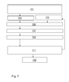
- Fig. 7 shows a diagram of a method for determining structure parameters according to an embodiment.
- the method comprises the step 701 for defining output parameters such as available light intensity I 0 in a relevant spectral area, sensor sensitivity S, minimum and maximum measurable signal values O and A, geometrical configuration such as transmittive or reflective devise geometry, distances and light incidence angles.
- output parameters such as available light intensity I 0 in a relevant spectral area, sensor sensitivity S, minimum and maximum measurable signal values O and A, geometrical configuration such as transmittive or reflective devise geometry, distances and light incidence angles.
- step 703 the optimum signal ⁇ I ⁇ S from an arrangement is determined.
- the structure parameters can be used for manufacturing the identity card with arranging a first arrangement of light reflecting elements in a first card body area of a card body and a second arrangement of light reflecting elements in a second card body area of the card body, the first arrangement of light reflecting elements having a higher light reflectivity than the second arrangement of light reflecting elements, preferential calculated corresponding to the related light scattering processes, e.g. to formula (2), the arrangements of light reflecting elements forming a physical unclonable function.
- the identity card is intended to be operated in contactless mode, which means that only limited power is available for the operation of sensors and light sources.
- LEDs Light Emitting Diodes
- CMOS technology CMOS technology
- the structure of the PUF can be used for generating an encryption key, wherein authentication by a challenge-response protocol directly using the unique mapping of challenges to responses of a PUF can be provided.
- material-based PUFs can be used where the measurement circuitry is integrated into the smartcard controller and the PUF structure is part of the card material surrounding the chip.
- PUF system is considered resistant against laser fault injection attacks and micro probing, since any physical change results in different measurement data and therefore in altered PUF responses.
Landscapes
- Engineering & Computer Science (AREA)
- Physics & Mathematics (AREA)
- General Physics & Mathematics (AREA)
- Multimedia (AREA)
- Theoretical Computer Science (AREA)
- Health & Medical Sciences (AREA)
- General Health & Medical Sciences (AREA)
- Vascular Medicine (AREA)
- Business, Economics & Management (AREA)
- Accounting & Taxation (AREA)
- Finance (AREA)
- Credit Cards Or The Like (AREA)
Abstract
Description
- The preset invention relates to identity cards with physical unclonable functions (PUF).
- Today, a wide variety of applications - from banking to access control to electronic passports - are based on identity cards, i.e. smart cards. These can be equipped with cryptographic modules and guarantee a high level of security for systems and users. However, designers and manufacturers of smartcards and security ICs are continuously aiming at further enhancing their cards' security.
- In order to further improve security of an identity card, Physical Unclonable Functions (PUFs) can be provided. PUFs are functions embodied in physical structures which are easy to evaluate but hard to predict. Furthermore, implementations are difficult to duplicate, even if the exact manufacturing process is known and available. Consequently, security architectures based on PUFs promise inherent unclonability, physical tamper resistance and secure establishment of device-unique cryptographic keys. Well-known bare silicon PUFs aim at ensuring the security of the circuit itself but do not grant tamper resistance to the card in which it is embedded.
- The challenge-response behaviour of a PUF is determined by sub-micron physical characteristics formed by manufacturing process variations which are not reproducible, not even by the original manufacturer. PUFs enable the generation of a device-unique secret based on physical properties rather than on binary memory mechanisms such as fuses. During the last decade, several PUF constructions have been proposed and realized as described in Lim, Daihyun and Lee, Jae W. and Gassend, Blaise and Suh, G. Edward and van Dijk, Marten and Devadas, Srinivas, Extracting secret keys from integrated circuits. In IEEE Transactions on Very Large Scale Integration (VLSI) Systems, volume 13, . Further reference is made to Thomas Esbach, Walter Fumy, Olga Kulikovska, Dominik Merli, Dieter Schuster, Frederic Stumpf, "A new security architecture for smartcards utilising PUFs", to be published in "Securing Electronic Business Processes - Highlights of the Information Security Solutions Europe 2012 Conference".
- PUFs are usually based on silicon structures and utilize tiny deviations in the electronic circuitry well below the tolerances of fabrication processes. These non-reproducible deviations make the circuitry unique and are often referred to as 'chip fingerprints'.
- However, in spite of intensive research, PUF implementations remain few and far between and are rarely considered in the context of high-end security architectures.
- It is therefore the object of the invention to provide an efficient concept for providing identity cards with a PUF.
- This object is achieved by the features of the independent claims. Further embodiments are disclosed in the description, the figures and the figures.
- The invention is based on the finding that the above object can be achieved by providing PUF structures with different reflectivities within a card body. Therefore, the intensity of the reflected light can be adapted to e.g. a sensitivity of an optical sensor sensing the reflected light.
- According to an aspect, the invention relates to an identity card, comprising a card body and a physical unclonable function arranged within the card body, wherein the physical unclonable function comprises a first arrangement of light reflecting elements being arranged in a first card body area, and a second arrangement of light reflecting elements being arranged in a second card body area, and wherein the first arrangement of light reflecting elements has a higher light reflectivity than the second arrangement of light reflecting elements.
- The reflectivity is determined as a fraction of reflected light by the respective arrangement of light reflecting elements. Preferably, all arrangement of light reflecting elements have reflectivities exceeding a predetermined threshold to ensure that some or each arrangement of light reflecting elements can reflect enough light to be sensed on a surface of the card body by the sensor. Thus, the required reflectivities of the arrangements of light reflecting elements can be determined in dependence on a sensitivity or resolution of an optical sensor sensing the reflected light on a surface of the card body or within the card body.
- The physical unclonable function is arranged to provide an optical fingerprint of the identity card or a kryptographic key. The card body can be at least partially light transparent and may be composed of one or more plastic layers such as polymer layers, in particular laminated plastic layers.
- The arrangement of light reflecting elements can be formed by metal layers respectively comprising a periodic pattern of metal stripes forming a grating. A plurality of such arrangement of light reflecting elements arranged above each other may uniquely diffract and/or refract and/or reflect incident light and thus form a unique fingerprint identifying the identity card. Such arrangement of light reflecting elements can be implemented when manufacturing an identity card, by e.g. embedding the arrangement of light reflecting elements in a plastic, e.g. polymer card body, or by arranging the arrangement of light reflecting elements between transparent laminate layers of the identity card.
- An advantage of such physical unclonable function is that it can comprise macroscopically well defined structures with non-random distribution in the card body which simplifies the manufacturing process and can allow optimization of light scattering in terms of sensitivity of the measuring system. At the same time, the uniqueness of each fabricated structure and correspondingly of its optical response can be provided by the smallest tolerances of the fabrication process on the microscopic level and thus is intrinsic to those PUFs.
- According to an embodiment, the second arrangement of light reflecting elements is arranged closer to at least one common point on a surface of the card body or within the card body than the first arrangement of light reflecting elements.
- According to an embodiment, the identity card comprises only arrangements of light reflecting elements, each having a reflectivity being greater than or equal to a predetermined reflectivity threshold, e.g. 5% or 10% the maximum reflectivity. Accordingly, the second arrangement of light reflecting may have a reflectivity of 100%.
- According to an embodiment, the identity card comprises only N arrangements of light reflecting elements, each of the N arrangements of light reflecting elements being arranged in a different card body area at a different distance from a common point on a surface of the card body or within the card body, and wherein a light reflectivity of the arrangements of light reflecting elements increases, in particular linearly or gradually, with increasing distance of the arrangements of light reflecting elements from the common point.
- According to an embodiment, the light reflecting elements of the first arrangement of light reflecting elements and of the second arrangement of light reflecting elements are respectively formed by back scattering or reflective particles being arranged to form the respective arrangement of light reflecting elements, or by planar surface elements, in particular stripes or rectangles or circular elements or oval elements, being arranged to form the respective arrangement of light reflecting elements. The planar surface elements can be formed of metal or polymer.
- According to an embodiment, a density of the light reflecting elements of the first arrangement of light reflecting elements in the first card body area is greater than a density of the light reflecting elements of the second arrangement of light reflecting elements in the second card body area.
- According to an embodiment, the light reflecting elements of the first arrangement of light reflecting elements have bigger reflective surfaces than the light reflecting elements of the second arrangement of light reflecting elements.
- According to an embodiment, the intensities of light reflected by the first arrangement of light reflecting elements and the second arrangement of light reflecting elements at a common point on a surface of the card body are identical within an identity range.
- According to an embodiment, the light reflecting elements of the respective arrangement of light reflecting elements are statistically or regularly arranged within the respective card body area.
- According to an embodiment, the light reflecting elements of the first arrangement of light reflecting elements and of the second arrangement of light reflecting elements respectively form reflective layers.
- According to an embodiment, the reflective layers are planar reflective layers arranged at different distances with respect to a surface of the card body, or wherein the reflective layers are arranged along curvatures, in particular spherical curvatures, with different radiuses towards a common center point, the common center point being a common point on a surface of the card body or being above or beneath the surface of the card body or within the card body.
- According to an embodiment, the light reflecting elements of the first arrangement of light reflecting elements and the light reflecting elements of the second arrangement of light reflecting elements are respectively arranged to form a periodic pattern, in particular a grating.
- According to an embodiment, a difference between the reflectivity of the first arrangement of light reflecting elements and the second arrangement of light reflecting elements is greater than or equal to a predetermined threshold. The predetermined threshold can be e.g. determined by a fraction resulting from dividing 100% by a number of arrangements of light reflecting elements. However, the predetermined threshold can be set to 5% or 10% the reflectivity of the most reflective arrangement of light reflecting elements. Moreover, the threshold can be defined by the light sensitivity or light resolution of an optical sensor which may sense the reflected light.
- According to an embodiment, the first arrangement of light reflecting elements and the second arrangement of light reflecting elements jointly form an optical lens.
- According to an embodiment, the card body is transparent and wherein the respective card body area forms a layer of the card body, in particular a laminate layer.
- According to an embodiment, the identity card further comprises a light source for emitting light towards the first arrangement of light reflecting elements and the second arrangement of light reflecting elements, and an optical sensor for sensing light reflected from the first arrangement of light reflecting elements and the second arrangement of light reflecting elements.
- According to an embodiment, the first arrangement of light reflecting elements and the second arrangement of light reflecting elements have light transmittances which are smaller than a light transmittance of the card body. The first arrangement of light reflecting elements and the second arrangement of light reflecting elements can be e.g. refractive layers and/or diffractive layers and/or reflective layers and/or reflective layers and/or at least partially opaque layers. Thereby, an optical fingerprint of the identity card can be obtained.
- According to an embodiment, the respective light transmittance layer is an optically linear layer or an optically nonlinear or optically excited layer.
- According to an embodiment, the optically linear layer is one of the following layers: a metal layer or a printing ink layer or a nanoparticle layer or a layer having a light refraction index which is different, e.g. greater, than a light refractive index of the card body, or a diffractive layer, wherein the optically nonlinear layer is a nonlinear polymer or photochrome layer, and wherein the optically excited layer is a fluorescent material layer.
- According to an embodiment, the first arrangement of light reflecting elements and the second arrangement of light reflecting elements are arranged above each other, e.g. exactly each other within a tolerance, e.g. 1% or 5% or displaced with respect to each other.
- According to an embodiment, the first arrangement of light reflecting elements and/or the second arrangement of light reflecting elements comprises spaced surface elements, in particular stripes or rectangles or circular elements or oval elements. The term "surface elements" denotes flat elements having a thickness smaller than e.g. a surface radius or a surface circumference or a surface width or a distance between the layers. The surfaces can be planar surfaces. Unlike particles, the surfaces of the surface elements are formed by surface areas which can be directed towards e.g. a light source arranged on the card body.
- According to an embodiment, the first arrangement of light reflecting elements comprises a periodic pattern, in particular a grating, of spaced surface elements having smaller transmittance than the card body, and wherein the second arrangement of light reflecting elements comprises a periodic pattern, in particular a grating, of spaced surface elements having smaller transmittance than the card body.
- According to an embodiment, the respective periodic pattern is one-dimensional or two-dimensional. The respective one-dimensional periodic pattern may comprise a plurality of stripes arranged next to each other so as to form a periodic structure. The respective two-dimensional periodic pattern may comprise a plurality of areas periodically arranged so as to form a two-dimensional grid.
- According to an embodiment, the first arrangement of light reflecting elements comprises a first periodic pattern of spaced surface elements, wherein the second arrangement of light reflecting elements comprises a second periodic pattern of spaced surface elements, and wherein the first periodic pattern of spaced surface elements and the second periodic pattern of spaced surface elements are arranged above each other. The spacing between the spaced surface elements can have a wavelength-scale dimension.
- According to an embodiment, the spaced surface elements of the first arrangement of light reflecting elements and the spaced surface elements of the second arrangement of light reflecting elements are arranged exactly above each other within a tolerance, e.g. 1%, 2% or 5% of a surface width, or wherein the first periodic pattern and the second periodic pattern are displaced with respect to each other.
- According to an embodiment, the spaced surface elements of the first arrangement of light reflecting elements have bigger or wider surfaces than the spaced surface elements of the second arrangement of light reflecting elements. Thus, the surface elements of the first arrangement of light reflecting elements may extend over the surface elements of the second arrangement of light reflecting elements.
- According to an embodiment, the respective arrangement of light reflecting elements comprises spaced surface elements respectively having a wavelength-scale surface dimensions or thicknesses, or wherein the respective arrangement of light reflecting elements comprises spaced surface elements respectively spaced apart by a wavelength-scale distance, or wherein a distance between the first arrangement of light reflecting elements and the second arrangement of light reflecting elements is of wavelength scale.
- According to an embodiment, the card body comprises laminated transparent layers, wherein the first arrangement of light reflecting elements is arranged between successive two laminated transparent layers of the card body, and wherein the second arrangement of light reflecting elements is arranged between successive two laminated transparent layers of the card body.
- According to an embodiment, the identity card further comprises a light source for emitting light towards the first arrangement of light reflecting elements and the second arrangement of light reflecting elements, and an optical sensor for sensing light from the first arrangement of light reflecting elements and the second arrangement of light reflecting elements in response to the emitted light. The light source and the optical sensor are arranged on a surface of the card body such that the second transmittance reduction layer is closer to the optical sensor than the first transmittance reduction layer.
- According to an embodiment, the identity card comprises an integrated circuit comprising the optical sensor. The integrated circuit may be formed by an ID chip arranged on a surface of the card body.
- According to an embodiment, the identity card is an identity document or a smart card or a credit card.
- According to an embodiment, the identity card is formed by a transparent polymer. The identity card can have a plurality of laminated polymer layers.
- According to a further aspect, the invention relates to a method for manufacturing an identity card, the method comprising arranging a first arrangement of light reflecting elements in a first card body area of a card body and a second arrangement of light reflecting elements in a second card body area of the card body, the first arrangement of light reflecting elements having a higher light reflectivity than the second arrangement of light reflecting elements, the arrangements of light reflecting elements forming a physical unclonable function.
- Further method steps of the method for generating an identity card are directly derivable from the features of the identity card.
- Further embodiments will be described with respect to the accompanying figures, in which:
-
Fig. 1a, 1b show identity cards with a PUF; -
Fig. 2 shows an identity card; -
Figs. 3a, 3b show stacks of arrangements of light reflecting elements; -
Figs. 4a ,4b show calculated intensities of light; -
Fig. 5 shows a schematic diagram of a stack of three arrangements of light reflecting elements; -
Fig. 6a ,6b and 6c show shows the arrangement of light reflecting elements; and calculated distributions of light intensity caused by the arrangements; and -
Fig. 7 shows a diagram of a method for determining structure parameters. -
Figs. 1 a and 1 b show identity cards according to some embodiments. - The
identity card 100 shown inFig. 1a comprises acard body 101 with aPUF 103 which is arranged within acard body 101. - The
PUF 103 comprises afirst arrangement 105 of light reflecting elements being arranged in a firstcard body area 107, and asecond arrangement 109 of light reflecting elements being arranged in a secondcard body area 111. Thefirst arrangement 105 of light reflecting elements has a higher light reflectivity than thesecond arrangement 109 of light reflecting elements. - The
first arrangement 105 of light reflecting elements and thesecond arrangement 109 of light reflecting elements can be formed by planar reflective layers extending parallel to asurface 113 of thecard body 101 and having surfaces e.g. showing towards thesurface 113. Thus, light emitted from thesurface 113 can be reflected by the reflective surfaces and measured on thesurface 113 e.g. by an optical sensor, which can be arranged on thesurface 113. - The layers can be formed by reflective metal layers comprising e.g. metal stripes as light reflecting elements.
-
Fig. 1b shows anidentity card 120 which comprises acard body 121 with aPUF 121 which is arranged within acard body 121. - The
PUF 123 comprises afirst arrangement 125 of light reflecting elements being arranged in a firstcard body area 127, and asecond arrangement 129 of light reflecting elements being arranged in a secondcard body area 131. Thefirst arrangement 125 of light reflecting elements has a higher light reflectivity than thesecond arrangement 129 of light reflecting elements. - The
first arrangement 125 of light reflecting elements and thesecond arrangement 129 of light reflecting elements can be formed by reflective layers which are arranged along curvatures, in particular spherical curvatures, with different radiuses towards a common center point, acommon center point 135 being a common point on a surface of the card body or being above or beneath the surface of the card body. The layers can be formed by reflective metal layers comprising e.g. metal stripes as light reflecting elements. - According to some embodiments, a device-unique material structure forming the PUF as e.g. key storage or optical fingerprint can be used which can have multiple advantages. One of them is the physical and logical connection between chip and card body. Furthermore, invasive manipulations would probably change or destroy the material and thereby render the embedded secret useless.
- For the scenario of an identity card of a smartcard, the choice of an optical PUF is favourable. Optical measurements are robust against Electro-Magnetic Interference (EMI) and in addition not only enable the use of the card body as the physical structure to be measured, but also provide the possibility of involving the printing on the card. However, resource constraints in smartcards, e. g. limited power consumption as well as static placement of the optical measurement mechanisms, do not allow the integration of optical PUFs based on laser beams.
- In general, the challenge-response behaviour of the
PUF 101 can be complex in order to resist model-building attacks and to provide enough entropy for the desired applications. - According to some embodiments, the
PUF PUF PUF -
Fig. 2 shows anidentity card 200, comprising acard body 201 and a physicalunclonable function card body 201, wherein the physical unclonable function comprises a first arrangement oflight reflecting elements 203 and a second arrangement oflight reflecting elements 207. - The first arrangement of
light reflecting elements 203 comprises spacedsurface elements 205, e.g. metal stripes, being arranged to form a one dimensional periodic pattern (grating). Accordingly, the second arrangement oflight reflecting elements 207 comprises spacedsurface elements 209, e.g. metal stripes, being arranged to form a one dimensional periodic pattern (grating). The first arrangement oflight reflecting elements 203 and the second arrangement oflight reflecting elements 207 are arranged above each other within thecard body 201, which is more transparent than the spacedsurface elements card body 201 can be formed from at least partially transparent polymer. - The
surface elements light source 211 arranged on top of thecard body 201. Thelight source 211 may comprise e.g. a LED or a LED array. Thus, the surfaces of thesurface elements light source 211 towards thesurface elements - The identity card can further comprise a
sensor 213 for sensing light from thesurface elements light source 211. - The
light source 211 and the sensor can be integrated within anintegrated circuit 215, - The first arrangement of
light reflecting elements 203 and the second arrangement oflight reflecting elements 207 collectively form the PUF as a probed physical structure arranged in a probed volume Vp . - The maximum amount of information that can be extracted from a PUF increases with the space that can be measured e.g. by the chip, i.e. the
integrated circuit 215. The card area that can be accessed by the measurement is the probed volume Vp . - According to some embodiments, the size of the probed area is defined on the one hand by chip specifications - such as measurement sensitivity and relative positions of light sources and sensors - and on the other hand by the scattering properties of the card materials. The optical properties can be optimized in terms of both the sensitivity of the sensors and the desired penetration depth. A parameter which can be considered is the back-scattering of light, since the sensors on the chip measure only the light that is reflected or scattered back to the
integrated circuit 215. This can be demonstrated using the one-dimensional model structure consisting of N equal partially reflective layers, each with reflection R.
- Intensities of light emitted and reflected by a single layer n are given by formula Itn = (1 - R)I t(n-1) and Irn = RI t(n-1) respectively, where I t(n-1) is intensity of light emitted by the previous layer. The total intensity of light reflected by the stack of k layers is given by formula

-
Fig. 3a shows a stack of k (k∈ {1...N}) arrangements oflight reflecting elements 301 collectively forming a PUF and being arranged in a volume having a thickness D. A space between subsequent arrangements oflight reflecting elements 301 is denoted by dn. The arrangement oflight reflecting elements 301 may be reflective layers respectively comprising a grating of surface elements such as metal stripes. -
Fig. 3b shows a stack of k (k∈ {1...N}) arrangement oflight reflecting elements 303 collectively forming a PUF. According to some embodiments, the reflectivities of the arrangements oflight reflecting elements 301 increase with increasing distance from a surface of a card body or from a plane in a card body, i.e. with increasing z along the z-axis. This is depicted inFig. 3a with increasing thicknesses of the horizontal lines representing the respective arrangement oflight reflecting elements 301. The light with the Intensity I0 is transmitted towards the arrangements oflight reflecting elements 301 from a surface of a card body, which is not depicted inFig. 3b . - In the following, a layer n in the stack of layers {1,2, ...n...N} will exemplarily be considered, wherein the
layer 1 is assumed to be closest one to the incidence plane.
Each layer is defined by its reflection coefficient rn and transmission coefficient tn - The intensity I0n is incident on the layer n. Then the reflected intensity Irn is given by Irn = I 0 nrn and the transmitted intensity by Itn Itn = I 0 ntn = I 0n (1-rn )
- Sensor signal caused by a single layer n is given by ΔIn = Irn = I 0 nrn
- For calculation of layer properties, the following can be assumed:
- A signal from a single layer can be measured by the sensor only if it exceeds the sensor sensitivity S: ΔIn ≥ S
- The dynamic range of the sensor is used most efficiently if the signal from a single layer is equal to the sensor sensitivity S: ΔIn = S and ΔI 1 = ΔI 2 = ... = ΔIn = ...ΔIN = S
- For the sake of simplicity, multiple reflections by layers are neglected, and only one reflection on each layer will be considered without loss of generality.
- Incidence intensity on layer n is I 0n = I 0(n-1)(1-rn ), with signal caused (reflected) by layer n:
- ΔIn = I 0 nrn = I 0(n-1)(1-rn )rn. A signal caused by layer (n-1) is ΔI n-1 = I 0(n-1) r n-1, and signals from all layers should be equal: ΔI n-1 = ΔIn, so that

- If the reflection coefficients of layers {1, 2, ...n...N} are defined by the formula (2), each layer will reflect the same light intensity and thus cause the same signal of the sensor.
-
Fig. 4a and4b depict the intensities of light emitted and reflected by the stack of k (k∈ {1...N}) arrangements oflight reflecting elements 301 as well as the intensity of light reflected by a single layer n. In particular, normalized intensities of light transmitted 401 (solid line), reflected 403 by the stack of k layers (circles) and reflected 405 by a single layer n (triangles) calculated corresponding to the formula (1) and (2) are shown inFig. 4a andFig. 4b relatively. - The contribution from a single layer decreases with the layer number n. For example, if a single layer reflects 10% of light (R=10%), the maximum contribution from a single layer to the signal does not exceed 10% and the contribution from the 24th layer becomes smaller than 1%. The contribution from the remaining N-24 layers does not exceed 8% of the total signal. This model clearly shows the relation between sensitivity of sensor, material structure and the maximum size of the probed physical structure. In the embodiment shown in
Fig. 4a , layer n from {1, 2, ...n...N} has the same reflection coefficient rn=0,1. - As shown in
Fig. 4b , each layer n from {1, 2, ... n...N} has a different reflection coefficient calculated corresponding to formula (2). The layer n=1 reflects 1% of incident light and the layer N=100 reflects 100% of incident light. - In the case of a stack of the equally reflecting layers shown in
Fig. 4a , the signal from the layer n=25 becomes smaller than 1 % of incident intensity. Thus a stack of maximum 25 layers can be used with sensor having sensitivity of 0,01. - In the case of a layer stack with gradual distribution of reflection as shown in
Fig. 4b , the signals from all layers are equal and amounts 1 % of incident intensity. A sensor with sensitivity of 0,01 can detect the signals from a stack of 100 layers. - In this way the stack of layer can be optimized in order to provide the higher detected volume of the material and thus the higher information content of the PUF.
- The approach can be applied to any light scattering layers or media by taking into account the related light scattering processes.
- The maximum amount of information that can be obtained from a probed area with an optical PUF can be roughly estimated, assuming that the smallest material structure that can be resolved by optical measurement has a size comparable to the wavelength λ of the probing light. The probed volume Vp can be divided into Ne elementary volumes λ3. In the simplest case, each elementary volume represents 1 bit of information and the maximum amount of information is given by the number of elementary volumes Ne = Vp / λ3.
- For example, from a volume Vp of size 1.0x1.0x0.3 mm3 probed by a wavelength of 700 nm, one can extract a maximum of 8.7x105 bits.
- With regard to light propagation and in order to describe the properties of light distribution at the exit surface of the medium, the influence of fabrication tolerances on the resulting light distribution and in order to relate the optimum medium structure and size to the integrated measuring means, the theoretical light propagation in the designed media can be calculated.
- The calculation approach can, by way of example, be based on elementary structures. A disordered structure is mathematically resolved into a finite series of elementary periodical structures. Light propagation in such structures can be numerically calculated in a volume compared to the probed volume Vp. Any single parameter of the structure, like the number of layers, period, contrast or spatial shift, can be independently varied and the resulting change in light distribution can be calculated.
-
Fig. 5 shows a schematic diagram of a stack of three arrangement oflight reflecting elements surface elements - The arrangement of
light reflecting elements surface elements -
Fig. 6a shows the arrangement oflight reflecting elements Fig. 5 , which are arranged within atransparent card body 601 of an identity card 600. The identity card further comprises a plurality oflight sources 603 and a plurality oflight sensors 605.Figs. 6b and 6c show corresponding light distributions obtained for reflective layer thicknesses of 10 nm,Fig. 6b , and 20 nm,Fig. 6c . - The arrangements of
light reflecting elements card body 601. The metal stripes can have different, e.g. staggered, widths as shown inFig. 6a . The cross section of the structure is shown schematically inFig 6a . The period Px between subsequent spaced surface elements can set to 50 µm (wavelength-scale), and the distance between the arrangement oflight reflecting elements - The thickness of the arrangement of
light reflecting elements - The graphs of
Figs. 6b and 6c show the resulting spatial distributions of light intensity normalized to the intensity of incident light. There is a difference in the light distribution for the different metal layer thicknesses of 10 and 30 nm. The latter results in a focussed light thus in even a further improved contrast of the light pattern. Furthermore, the light is redistributed by the structure in the entire calculated volume while the distribution changes with distance from the structure. The light achieves higher contrast at some distance, while in the area close to the structure the contrast and the characteristic size of the light spots remain smaller. The results show how the light distribution is affected by a 20 nm difference in layer thickness. - In the following, the material selection for the arrangement of light reflecting elements will be addressed.
- The arrangement of light reflecting elements can have a different light characteristic, e.g. transmittance, then the card body surrounding the arrangement of light reflecting elements. According to some embodiments, the arrangement of light reflecting elements can be structured using known card production techniques, including printing, spraying, dispersing, embossing or vacuum deposition techniques as well as holographic recording.
- Most optical materials do not interact with light, thus providing simultaneous and linear response. The signal from a PUF based on such materials is measured by a sensor at the same moment as the light is emitted by a light source and its value is proportional to the intensity of the probe light.
- Under the assumption that sensors integrate light over time tm , the type of suitable materials can be extended by material that can interact with light within time < tm . Optically non-linear materials change their optical properties under irradiation. This change is strongly dependent on the light intensity, is induced within a very short time and relaxes after the light is switched off. Fluorescent materials absorb light in one spectral region and emit it in another, usually red-shifted, spectral region. Emission follows absorption within a very short time and depends strongly on the molecular surroundings of the emitting units. Typical emission times are within the range of 0.5 to 20 ns.
- Of particular interest are time-resolved or time-delayed measurements, where the response is measured with some delay relative to the probe light flash. An approach of this kind only makes sense if the material response changes reversibly during or after irradiation. Photochromic materials are examples of such materials. Under irradiation with actinic light, the photochromic unit undergoes a transformation to its other form, which has a different absorption spectrum. Relaxation to the initial form occurs thermally or under irradiation. The most effective photochromic materials are stilbenes, spiropyranes, azobenzenes as well as bacteriorhodopsin.
- The material types and their related properties are summarized in Table 1.
Table 1: Material overview and properties Material types Related properties Optically linear: Simultaneous response: printing inks, metallic inks, dispersed micro and nanoparticles, materials with high refractive indices response depends on light intensity; broadband absorption spectra; probing with different wavelengths is desirable in order to increase variation of PUF response. Optically nonlinear: Simultaneous response: variety of nonlinear polymers, bacteriorhodopsin response changes with time, but the response time is very short (shorter than measurement time); response depends on light intensity; nonlinear effects require very high light intensities or electrical fields. - Regarding the light generation and measurement, the integration of light sources and sensors into the security chip (integrated circuit) that is embedded in the identity card can be performed.
- According to some embodiments, a PUF model can be provided which takes into account the limitations of available volume, light intensity and resolution or sensitivity of a light sensor for sensing the reflected light. The PUF model can be used for manufacturing an identity card with the modelled PUF structure.
- According to some embodiments, the PUF has non-homogeneously distributed scattering or reflection centres or parameters. Such structures enable optimization of a PUF volume.
- In order to determine the PUF structure, a simplified model can be used according to some embodiments. In a first step, the card volume or any medium can be presented as a stack of basic layers which enable a simple comparison of optical characteristics between layers. Upon the basis of the basic layers, a maximal senseable volume, a maximum number of layers and a maximum optical density of the respective layer can be determined. The PUF arrangements can thereafter be defined such that the reflected light intensities of light reflected by the respective arrangement are equal within a tolerance, say 1%, 2% or 5%. This enables to determine an optimum volume for embedding the PUF.
- Therefore, unnecessary layers which cannot be sensed by optical sensors can be avoided. Further, the PUF volume can be adapted to the volume of the card body. This approach can also be used for statistical PUF arrangements.
- According to some embodiments, the identity card comprises at least one light source and at least one sensor, which can be integrated in the card body.
- The card body can be subdivided into layers forming PUF arrangements. Each layer reflects a fraction, e.g. the same fraction, of incident, i.e. transmitted light. Therefore, the reflected light intensity measurable on a surface of the card body can decrease with increasing distance of the respective layer to the surface of the card body. Therefore, the N layers forming N arrangements of the PUF generate refelected light with different intensities at the optical sensor, sothat the N layers are differently represented in the total reflected light sensed at the durface of the card body.
- In order t o achieve that the measurable intensities of reflected light by each arrangement are the same within a tolerance, e.g. 2% or 5%, the reflectivities of different arrangements are different and can increase with increasing distance from the surface of the card body.
- According to some embodiments, an optical sensor can have a measurement range extending between minimal measured signal O and a maximal measured signal A. A minimum resolvable signal difference or signal change is denoted by S. Thus, the maximum number of resolvable signals is p=(A-O)/S.
- Each arrangement reflects a fraction of the incident light denoted by Irn and transmits a fraction denoted by Itn.
- In order to ensure that the reflected light intensity Irn can be measured by the sensor, the following conditions can be satisfied:

- The difference or the change of the total signal caused by one damaged or omitted arrangement can be used to obtain ΔIn=Irn→S.
- Thus, a maximum number of arrangements is N→p, or N≤p for signals ≥S.
-
Fig. 7 shows a diagram of a method for determining structure parameters according to an embodiment. - The method comprises the
step 701 for defining output parameters such as available light intensity I0 in a relevant spectral area, sensor sensitivity S, minimum and maximum measurable signal values O and A, geometrical configuration such as transmittive or reflective devise geometry, distances and light incidence angles. - In
step 703, the optimum signal ΔI≥S from an arrangement is determined. - In
step 705, a maximum number N of arrangements is determined such that N=(A-O)/S. - In
step 707, the thicknesses d, D and the layers number N with d=D/N can be determined, see alsoFigs. 3a and 3b . - In
step 709, optical parameters of the arrangements such as reflectivity rn can be determined, such that the measurable intensities of light reflected by the respective arrangement are equal within a tolerance, e.g. 2% or 5%, i.e. I1=I2=....=In=... =IN. - In
step 711, parameter verification can be performed in terms of possibilities and limits of fabrication processes to e.g. determine whether a minimum reflectivity rM and corresponding a minimum reflected signal M that can be reached by the applied fabrication method and used materials fulfill M ≥ S and/or rM ≥ {r1, r2, ...rN}. If the verification fails, then the method continues withoptional step 713, where a target smallest signal S from one arrangement can be corrected by setting S=M. - Otherwise, structure parameter such as reflectivities are outputted in
step 713. - The structure parameters can be used for manufacturing the identity card with arranging a first arrangement of light reflecting elements in a first card body area of a card body and a second arrangement of light reflecting elements in a second card body area of the card body, the first arrangement of light reflecting elements having a higher light reflectivity than the second arrangement of light reflecting elements, preferential calculated corresponding to the related light scattering processes, e.g. to formula (2), the arrangements of light reflecting elements forming a physical unclonable function.
- According to some embodiments, the identity card is intended to be operated in contactless mode, which means that only limited power is available for the operation of sensors and light sources.
- Regarding the light source, Light Emitting Diodes (LEDs) can be used as light sources since they can be fabricated using CMOS technology and therefore can be easily integrated on a security IC according to an embodiment.
- According to some embodiments, the structure of the PUF can be used for generating an encryption key, wherein authentication by a challenge-response protocol directly using the unique mapping of challenges to responses of a PUF can be provided.
- According to some embodiments, material-based PUFs can be used where the measurement circuitry is integrated into the smartcard controller and the PUF structure is part of the card material surrounding the chip. Such PUF system is considered resistant against laser fault injection attacks and micro probing, since any physical change results in different measurement data and therefore in altered PUF responses.
Claims (15)
- Identity card, comprising:a card body (101, 121); anda physical unclonable function (103, 123) arranged within the card body (101, 121), wherein the physical unclonable function (103, 123) comprises a first arrangement of light reflecting elements (105, 125) being arranged in a first card body area (107, 127), and a second arrangement of light reflecting elements (109, 129) being arranged in a second card body area (111, 131), and wherein the first arrangement of light reflecting elements (105, 125) has a higher light reflectivity than the second arrangement of light reflecting elements (109, 129).
- The identity card of claim 1, wherein the second arrangement of light reflecting elements (109, 129) is arranged closer to at least one common point (135) on a surface (113, 133) of the card body (101, 121) or within the card body (101, 121) than the first arrangement of light reflecting elements (105, 125).
- The identity card of claim 1 or 2, comprising only N arrangements (103, 123) of light reflecting elements, each of the N arrangements (103, 123) of light reflecting elements being arranged in a different card body area at a different distance from a common point (135) on a surface (113, 133) of the card body (101, 121) or in the card body (101, 121), and wherein a light reflectivity of the arrangements (103, 123) of light reflecting elements increases, in particular linearly or gradually, with increasing distance of the arrangements (103, 123) of light reflecting elements from the common point (133).
- The identity card of any of the preceding claims, wherein the light reflecting elements of the respective arrangement (105, 109, 125, 129) of light reflecting elements are respectively formed by back scattering or reflective particles being arranged to form the respective arrangement of light reflecting elements (105, 109, 125, 129), or by planar surface elements, in particular stripes or rectangles or circular elements or oval elements, being arranged to form the respective arrangement of light reflecting elements (105, 109, 125, 129).
- The identity card of any of the preceding claims, wherein a spatial density of the light reflecting elements of the first arrangement (105, 125) of light reflecting elements in the first card body area (107, 127) is greater than a density of the light reflecting elements of the second arrangement (109,129) of light reflecting elements in the second card body area (111, 131).
- The identity card of any of the preceding claims, wherein the light reflecting elements of the first arrangement (105, 125) of light reflecting elements have bigger reflective surfaces than the light reflecting elements of the second arrangement (109,129) of light reflecting elements.
- The identity card of any of the preceding claims, wherein the intensities of light reflected by the first arrangement (105, 125) of light reflecting elements and the second arrangement (109,129) of light reflecting elements at a common point on a surface of the card body are identical within an identity range.
- The identity card of any of the preceding claims, wherein the light reflecting elements of the respective arrangement (105, 109, 125, 129) of light reflecting elements are statistically or regularly arranged within the respective card body area.
- The identity card of any of the preceding claims, wherein the light reflecting elements of the first (105, 125) arrangement of light reflecting elements and of the second arrangement (109,129) of light reflecting elements respectively form reflective layers.
- The identity card of claim 9, wherein the reflective layers are planar reflective layers arranged at different distances with respect to a surface of the card body, or wherein the reflective layers are arranged along curvatures, in particular spherical curvatures, with different radiuses towards a common center point, the common center point being a common point (133) on a surface of the card body (113, 133) or being above or beneath the surface of the card body or within the card body (101, 121).
- The identity card of any of the preceding claims, wherein the light reflecting elements of the respective arrangement of light reflecting elements (105, 109, 125, 129) are respectively arranged to form a periodic pattern, in particular a grating.
- The identity card of any of the preceding claims, wherein a difference between the reflectivity of the first arrangement of light reflecting elements (105, 125) and the second arrangement (109, 129) of light reflecting elements is greater than or equal to a predetermined threshold.
- The identity card of any of the preceding claims, wherein the card body (101, 121) is transparent and wherein the respective card body area forms a layer of the card body, in particular a laminate layer.
- The identity card of any of the preceding claims, further comprising a light source for emitting light towards the first arrangement of light reflecting elements and the second arrangement of light reflecting elements, and an optical sensor for sensing light reflected from the first arrangement of light reflecting elements and the second arrangement of light reflecting elements.
- Method for manufacturing an identity card, the method comprising:arranging a first arrangement of light reflecting elements in a first card body area of a card body and a second arrangement of light reflecting elements in a second card body area of the card body, the first arrangement of light reflecting elements having a higher light reflectivity than the second arrangement of light reflecting elements, the arrangements of light reflecting elements forming a physical unclonable function.
Priority Applications (2)
| Application Number | Priority Date | Filing Date | Title |
|---|---|---|---|
| EP12188964.6A EP2722192B1 (en) | 2012-10-18 | 2012-10-18 | Identity card with a physical unclonable function |
| PCT/EP2013/064831 WO2014060125A1 (en) | 2012-10-18 | 2013-07-12 | Identity card with a physical unclonable function |
Applications Claiming Priority (1)
| Application Number | Priority Date | Filing Date | Title |
|---|---|---|---|
| EP12188964.6A EP2722192B1 (en) | 2012-10-18 | 2012-10-18 | Identity card with a physical unclonable function |
Publications (2)
| Publication Number | Publication Date |
|---|---|
| EP2722192A1 true EP2722192A1 (en) | 2014-04-23 |
| EP2722192B1 EP2722192B1 (en) | 2015-09-16 |
Family
ID=47146189
Family Applications (1)
| Application Number | Title | Priority Date | Filing Date |
|---|---|---|---|
| EP12188964.6A Active EP2722192B1 (en) | 2012-10-18 | 2012-10-18 | Identity card with a physical unclonable function |
Country Status (2)
| Country | Link |
|---|---|
| EP (1) | EP2722192B1 (en) |
| WO (1) | WO2014060125A1 (en) |
Cited By (1)
| Publication number | Priority date | Publication date | Assignee | Title |
|---|---|---|---|---|
| DE102015120315A1 (en) * | 2015-11-24 | 2017-05-24 | Bundesdruckerei Gmbh | Identification document and method for identifying a person |
Citations (6)
| Publication number | Priority date | Publication date | Assignee | Title |
|---|---|---|---|---|
| US4066280A (en) * | 1976-06-08 | 1978-01-03 | American Bank Note Company | Documents of value printed to prevent counterfeiting |
| DE2838795A1 (en) * | 1978-09-06 | 1980-03-20 | Hoechst Ag | IDENTIFICATION CARD |
| GB2304077A (en) * | 1995-06-30 | 1997-03-12 | Andrew John Farrall | Security device comprising reflective particles |
| EP0778159A1 (en) * | 1995-04-26 | 1997-06-11 | I.D. Tec, S.L. | Security covering structure for identity documents, and process for obtaining it |
| WO2006056089A2 (en) * | 2004-11-23 | 2006-06-01 | Orell Füssli Sicherheitsdruck Ag | Security document comprising a light source and a light-processing device |
| WO2007087498A2 (en) * | 2006-01-23 | 2007-08-02 | Digimarc Corporation | Methods, systems, and subcombinations useful with physical articles |
-
2012
- 2012-10-18 EP EP12188964.6A patent/EP2722192B1/en active Active
-
2013
- 2013-07-12 WO PCT/EP2013/064831 patent/WO2014060125A1/en not_active Ceased
Patent Citations (6)
| Publication number | Priority date | Publication date | Assignee | Title |
|---|---|---|---|---|
| US4066280A (en) * | 1976-06-08 | 1978-01-03 | American Bank Note Company | Documents of value printed to prevent counterfeiting |
| DE2838795A1 (en) * | 1978-09-06 | 1980-03-20 | Hoechst Ag | IDENTIFICATION CARD |
| EP0778159A1 (en) * | 1995-04-26 | 1997-06-11 | I.D. Tec, S.L. | Security covering structure for identity documents, and process for obtaining it |
| GB2304077A (en) * | 1995-06-30 | 1997-03-12 | Andrew John Farrall | Security device comprising reflective particles |
| WO2006056089A2 (en) * | 2004-11-23 | 2006-06-01 | Orell Füssli Sicherheitsdruck Ag | Security document comprising a light source and a light-processing device |
| WO2007087498A2 (en) * | 2006-01-23 | 2007-08-02 | Digimarc Corporation | Methods, systems, and subcombinations useful with physical articles |
Non-Patent Citations (2)
| Title |
|---|
| LIM, DAIHYUN; LEE, JAE W.; GASSEND, BLAISE; SUH, G. EDWARD; VAN DIJK, MARTEN; DEVADAS, SRINIVAS: "Extracting secret keys from integrated circuits", IEEE TRANSACTIONS ON VERY LARGE SCALE INTEGRATION (VLSI) SYSTEMS, vol. 13, no. 10, 2005, pages 1200 - 1205 |
| THOMAS ESBACH; WALTER FUMY; OLGA KULIKOVSKA; DOMINIK MERLI; DIETER SCHUSTER; FREDERIC STUMPF: "A new security architecture for smartcards utilising PUFs", SECURING ELECTRONIC BUSINESS PROCESSES - HIGHLIGHTS OF THE INFORMATION SECURITY SOLUTIONS EUROPE 2012 CONFERENCE |
Cited By (1)
| Publication number | Priority date | Publication date | Assignee | Title |
|---|---|---|---|---|
| DE102015120315A1 (en) * | 2015-11-24 | 2017-05-24 | Bundesdruckerei Gmbh | Identification document and method for identifying a person |
Also Published As
| Publication number | Publication date |
|---|---|
| WO2014060125A1 (en) | 2014-04-24 |
| EP2722192B1 (en) | 2015-09-16 |
Similar Documents
| Publication | Publication Date | Title |
|---|---|---|
| US9953253B2 (en) | Identity card with physical unclonable function | |
| EP2237183B1 (en) | Method for security purposes | |
| US8408470B2 (en) | Object for authentication verification, authentication verifying chip reading device and authentication judging method | |
| JP4914896B2 (en) | Especially safe and / or safe items such as valuable documents | |
| Du et al. | Unclonable optical fiber identification based on Rayleigh backscattering signatures | |
| CN103003827B (en) | Secure file or valuable document and its method for manufacture and checking | |
| JP2004171109A (en) | Device authentication system | |
| US8820639B2 (en) | Security feature RFID card | |
| Esbach et al. | A new security architecture for smartcards utilizing PUFs | |
| KR20110081973A (en) | Optical sensor | |
| US5875170A (en) | Optical data carriers and reading devices therefor | |
| US20100044431A1 (en) | card capable of authentication | |
| RU2435218C2 (en) | Card with possibility of authentication | |
| EP2722192B1 (en) | Identity card with a physical unclonable function | |
| KR102003164B1 (en) | Method of manufacturing an anti-counterfeit apparatus | |
| EP1527412B1 (en) | Security document comprising an integrated microcircuit connected to a measuring microcircuit | |
| CN113742796B (en) | Optical encryption security device for smart card, encryption method and smart card | |
| Tehranipoor et al. | Optical puf | |
| RU2608259C2 (en) | Method of improving protective properties of identification saw-mark | |
| CN101405753A (en) | Card capable of performing true/false judgment by a fluorescent particle chip | |
| Kulikovska et al. | A New Security Architecture for Smartcards Utilizing PUFs | |
| Patel et al. | Identification Key Based on Optical Variable Nanostructures | |
| KR20170029882A (en) | Manufacture method for card for counterfeit prevention | |
| HK1145160A (en) | Authenticity validation subject, authenticity validation chip reader, and authenticity judging method | |
| TW201032140A (en) | Embossed hologram chip and manufacturing method therefor |
Legal Events
| Date | Code | Title | Description |
|---|---|---|---|
| PUAI | Public reference made under article 153(3) epc to a published international application that has entered the european phase |
Free format text: ORIGINAL CODE: 0009012 |
|
| AK | Designated contracting states |
Kind code of ref document: A1 Designated state(s): AL AT BE BG CH CY CZ DE DK EE ES FI FR GB GR HR HU IE IS IT LI LT LU LV MC MK MT NL NO PL PT RO RS SE SI SK SM TR |
|
| AX | Request for extension of the european patent |
Extension state: BA ME |
|
| 17P | Request for examination filed |
Effective date: 20140414 |
|
| RBV | Designated contracting states (corrected) |
Designated state(s): AL AT BE BG CH CY CZ DE DK EE ES FI FR GB GR HR HU IE IS IT LI LT LU LV MC MK MT NL NO PL PT RO RS SE SI SK SM TR |
|
| 17Q | First examination report despatched |
Effective date: 20141208 |
|
| REG | Reference to a national code |
Ref country code: DE Ref legal event code: R079 Ref document number: 602012010591 Country of ref document: DE Free format text: PREVIOUS MAIN CLASS: B42D0025000000 Ipc: G06K0009000000 |
|
| GRAP | Despatch of communication of intention to grant a patent |
Free format text: ORIGINAL CODE: EPIDOSNIGR1 |
|
| RIC1 | Information provided on ipc code assigned before grant |
Ipc: G06K 9/00 20060101AFI20150427BHEP Ipc: B42D 25/00 20140101ALI20150427BHEP |
|
| INTG | Intention to grant announced |
Effective date: 20150522 |
|
| GRAS | Grant fee paid |
Free format text: ORIGINAL CODE: EPIDOSNIGR3 |
|
| GRAA | (expected) grant |
Free format text: ORIGINAL CODE: 0009210 |
|
| AK | Designated contracting states |
Kind code of ref document: B1 Designated state(s): AL AT BE BG CH CY CZ DE DK EE ES FI FR GB GR HR HU IE IS IT LI LT LU LV MC MK MT NL NO PL PT RO RS SE SI SK SM TR |
|
| REG | Reference to a national code |
Ref country code: GB Ref legal event code: FG4D |
|
| REG | Reference to a national code |
Ref country code: CH Ref legal event code: EP |
|
| REG | Reference to a national code |
Ref country code: IE Ref legal event code: FG4D |
|
| REG | Reference to a national code |
Ref country code: AT Ref legal event code: REF Ref document number: 750309 Country of ref document: AT Kind code of ref document: T Effective date: 20151015 |
|
| REG | Reference to a national code |
Ref country code: DE Ref legal event code: R096 Ref document number: 602012010591 Country of ref document: DE Ref country code: FR Ref legal event code: PLFP Year of fee payment: 4 |
|
| REG | Reference to a national code |
Ref country code: NL Ref legal event code: MP Effective date: 20150916 |
|
| PG25 | Lapsed in a contracting state [announced via postgrant information from national office to epo] |
Ref country code: GR Free format text: LAPSE BECAUSE OF FAILURE TO SUBMIT A TRANSLATION OF THE DESCRIPTION OR TO PAY THE FEE WITHIN THE PRESCRIBED TIME-LIMIT Effective date: 20151217 Ref country code: FI Free format text: LAPSE BECAUSE OF FAILURE TO SUBMIT A TRANSLATION OF THE DESCRIPTION OR TO PAY THE FEE WITHIN THE PRESCRIBED TIME-LIMIT Effective date: 20150916 Ref country code: LV Free format text: LAPSE BECAUSE OF FAILURE TO SUBMIT A TRANSLATION OF THE DESCRIPTION OR TO PAY THE FEE WITHIN THE PRESCRIBED TIME-LIMIT Effective date: 20150916 Ref country code: NO Free format text: LAPSE BECAUSE OF FAILURE TO SUBMIT A TRANSLATION OF THE DESCRIPTION OR TO PAY THE FEE WITHIN THE PRESCRIBED TIME-LIMIT Effective date: 20151216 Ref country code: LT Free format text: LAPSE BECAUSE OF FAILURE TO SUBMIT A TRANSLATION OF THE DESCRIPTION OR TO PAY THE FEE WITHIN THE PRESCRIBED TIME-LIMIT Effective date: 20150916 |
|
| REG | Reference to a national code |
Ref country code: LT Ref legal event code: MG4D |
|
| REG | Reference to a national code |
Ref country code: AT Ref legal event code: MK05 Ref document number: 750309 Country of ref document: AT Kind code of ref document: T Effective date: 20150916 |
|
| PG25 | Lapsed in a contracting state [announced via postgrant information from national office to epo] |
Ref country code: HR Free format text: LAPSE BECAUSE OF FAILURE TO SUBMIT A TRANSLATION OF THE DESCRIPTION OR TO PAY THE FEE WITHIN THE PRESCRIBED TIME-LIMIT Effective date: 20150916 Ref country code: SE Free format text: LAPSE BECAUSE OF FAILURE TO SUBMIT A TRANSLATION OF THE DESCRIPTION OR TO PAY THE FEE WITHIN THE PRESCRIBED TIME-LIMIT Effective date: 20150916 Ref country code: RS Free format text: LAPSE BECAUSE OF FAILURE TO SUBMIT A TRANSLATION OF THE DESCRIPTION OR TO PAY THE FEE WITHIN THE PRESCRIBED TIME-LIMIT Effective date: 20150916 |
|
| PG25 | Lapsed in a contracting state [announced via postgrant information from national office to epo] |
Ref country code: NL Free format text: LAPSE BECAUSE OF FAILURE TO SUBMIT A TRANSLATION OF THE DESCRIPTION OR TO PAY THE FEE WITHIN THE PRESCRIBED TIME-LIMIT Effective date: 20150916 |
|
| PG25 | Lapsed in a contracting state [announced via postgrant information from national office to epo] |
Ref country code: SK Free format text: LAPSE BECAUSE OF FAILURE TO SUBMIT A TRANSLATION OF THE DESCRIPTION OR TO PAY THE FEE WITHIN THE PRESCRIBED TIME-LIMIT Effective date: 20150916 Ref country code: ES Free format text: LAPSE BECAUSE OF FAILURE TO SUBMIT A TRANSLATION OF THE DESCRIPTION OR TO PAY THE FEE WITHIN THE PRESCRIBED TIME-LIMIT Effective date: 20150916 Ref country code: EE Free format text: LAPSE BECAUSE OF FAILURE TO SUBMIT A TRANSLATION OF THE DESCRIPTION OR TO PAY THE FEE WITHIN THE PRESCRIBED TIME-LIMIT Effective date: 20150916 Ref country code: CZ Free format text: LAPSE BECAUSE OF FAILURE TO SUBMIT A TRANSLATION OF THE DESCRIPTION OR TO PAY THE FEE WITHIN THE PRESCRIBED TIME-LIMIT Effective date: 20150916 Ref country code: IS Free format text: LAPSE BECAUSE OF FAILURE TO SUBMIT A TRANSLATION OF THE DESCRIPTION OR TO PAY THE FEE WITHIN THE PRESCRIBED TIME-LIMIT Effective date: 20160116 Ref country code: IT Free format text: LAPSE BECAUSE OF FAILURE TO SUBMIT A TRANSLATION OF THE DESCRIPTION OR TO PAY THE FEE WITHIN THE PRESCRIBED TIME-LIMIT Effective date: 20150916 |
|
| PG25 | Lapsed in a contracting state [announced via postgrant information from national office to epo] |
Ref country code: PT Free format text: LAPSE BECAUSE OF FAILURE TO SUBMIT A TRANSLATION OF THE DESCRIPTION OR TO PAY THE FEE WITHIN THE PRESCRIBED TIME-LIMIT Effective date: 20160118 Ref country code: PL Free format text: LAPSE BECAUSE OF FAILURE TO SUBMIT A TRANSLATION OF THE DESCRIPTION OR TO PAY THE FEE WITHIN THE PRESCRIBED TIME-LIMIT Effective date: 20150916 Ref country code: RO Free format text: LAPSE BECAUSE OF FAILURE TO SUBMIT A TRANSLATION OF THE DESCRIPTION OR TO PAY THE FEE WITHIN THE PRESCRIBED TIME-LIMIT Effective date: 20150916 Ref country code: AT Free format text: LAPSE BECAUSE OF FAILURE TO SUBMIT A TRANSLATION OF THE DESCRIPTION OR TO PAY THE FEE WITHIN THE PRESCRIBED TIME-LIMIT Effective date: 20150916 |
|
| REG | Reference to a national code |
Ref country code: CH Ref legal event code: PL |
|
| REG | Reference to a national code |
Ref country code: DE Ref legal event code: R097 Ref document number: 602012010591 Country of ref document: DE |
|
| PG25 | Lapsed in a contracting state [announced via postgrant information from national office to epo] |
Ref country code: MC Free format text: LAPSE BECAUSE OF FAILURE TO SUBMIT A TRANSLATION OF THE DESCRIPTION OR TO PAY THE FEE WITHIN THE PRESCRIBED TIME-LIMIT Effective date: 20150916 |
|
| PLBE | No opposition filed within time limit |
Free format text: ORIGINAL CODE: 0009261 |
|
| STAA | Information on the status of an ep patent application or granted ep patent |
Free format text: STATUS: NO OPPOSITION FILED WITHIN TIME LIMIT |
|
| REG | Reference to a national code |
Ref country code: IE Ref legal event code: MM4A |
|
| PG25 | Lapsed in a contracting state [announced via postgrant information from national office to epo] |
Ref country code: CH Free format text: LAPSE BECAUSE OF NON-PAYMENT OF DUE FEES Effective date: 20151031 Ref country code: LI Free format text: LAPSE BECAUSE OF NON-PAYMENT OF DUE FEES Effective date: 20151031 |
|
| 26N | No opposition filed |
Effective date: 20160617 |
|
| PG25 | Lapsed in a contracting state [announced via postgrant information from national office to epo] |
Ref country code: DK Free format text: LAPSE BECAUSE OF FAILURE TO SUBMIT A TRANSLATION OF THE DESCRIPTION OR TO PAY THE FEE WITHIN THE PRESCRIBED TIME-LIMIT Effective date: 20150916 |
|
| REG | Reference to a national code |
Ref country code: FR Ref legal event code: PLFP Year of fee payment: 5 |
|
| PG25 | Lapsed in a contracting state [announced via postgrant information from national office to epo] |
Ref country code: IE Free format text: LAPSE BECAUSE OF NON-PAYMENT OF DUE FEES Effective date: 20151018 |
|
| PG25 | Lapsed in a contracting state [announced via postgrant information from national office to epo] |
Ref country code: SI Free format text: LAPSE BECAUSE OF FAILURE TO SUBMIT A TRANSLATION OF THE DESCRIPTION OR TO PAY THE FEE WITHIN THE PRESCRIBED TIME-LIMIT Effective date: 20150916 |
|
| PG25 | Lapsed in a contracting state [announced via postgrant information from national office to epo] |
Ref country code: BE Free format text: LAPSE BECAUSE OF FAILURE TO SUBMIT A TRANSLATION OF THE DESCRIPTION OR TO PAY THE FEE WITHIN THE PRESCRIBED TIME-LIMIT Effective date: 20150916 |
|
| PG25 | Lapsed in a contracting state [announced via postgrant information from national office to epo] |
Ref country code: BG Free format text: LAPSE BECAUSE OF FAILURE TO SUBMIT A TRANSLATION OF THE DESCRIPTION OR TO PAY THE FEE WITHIN THE PRESCRIBED TIME-LIMIT Effective date: 20150916 Ref country code: HU Free format text: LAPSE BECAUSE OF FAILURE TO SUBMIT A TRANSLATION OF THE DESCRIPTION OR TO PAY THE FEE WITHIN THE PRESCRIBED TIME-LIMIT; INVALID AB INITIO Effective date: 20121018 Ref country code: SM Free format text: LAPSE BECAUSE OF FAILURE TO SUBMIT A TRANSLATION OF THE DESCRIPTION OR TO PAY THE FEE WITHIN THE PRESCRIBED TIME-LIMIT Effective date: 20150916 |
|
| PG25 | Lapsed in a contracting state [announced via postgrant information from national office to epo] |
Ref country code: CY Free format text: LAPSE BECAUSE OF FAILURE TO SUBMIT A TRANSLATION OF THE DESCRIPTION OR TO PAY THE FEE WITHIN THE PRESCRIBED TIME-LIMIT Effective date: 20150916 |
|
| PG25 | Lapsed in a contracting state [announced via postgrant information from national office to epo] |
Ref country code: MT Free format text: LAPSE BECAUSE OF FAILURE TO SUBMIT A TRANSLATION OF THE DESCRIPTION OR TO PAY THE FEE WITHIN THE PRESCRIBED TIME-LIMIT Effective date: 20150916 |
|
| REG | Reference to a national code |
Ref country code: FR Ref legal event code: PLFP Year of fee payment: 6 |
|
| PG25 | Lapsed in a contracting state [announced via postgrant information from national office to epo] |
Ref country code: LU Free format text: LAPSE BECAUSE OF NON-PAYMENT OF DUE FEES Effective date: 20151018 |
|
| PG25 | Lapsed in a contracting state [announced via postgrant information from national office to epo] |
Ref country code: MK Free format text: LAPSE BECAUSE OF FAILURE TO SUBMIT A TRANSLATION OF THE DESCRIPTION OR TO PAY THE FEE WITHIN THE PRESCRIBED TIME-LIMIT Effective date: 20150916 |
|
| REG | Reference to a national code |
Ref country code: FR Ref legal event code: PLFP Year of fee payment: 7 |
|
| PG25 | Lapsed in a contracting state [announced via postgrant information from national office to epo] |
Ref country code: TR Free format text: LAPSE BECAUSE OF FAILURE TO SUBMIT A TRANSLATION OF THE DESCRIPTION OR TO PAY THE FEE WITHIN THE PRESCRIBED TIME-LIMIT Effective date: 20150916 Ref country code: AL Free format text: LAPSE BECAUSE OF FAILURE TO SUBMIT A TRANSLATION OF THE DESCRIPTION OR TO PAY THE FEE WITHIN THE PRESCRIBED TIME-LIMIT Effective date: 20150916 |
|
| REG | Reference to a national code |
Ref country code: DE Ref legal event code: R079 Ref document number: 602012010591 Country of ref document: DE Free format text: PREVIOUS MAIN CLASS: G06K0009000000 Ipc: G06V0010000000 |
|
| P01 | Opt-out of the competence of the unified patent court (upc) registered |
Effective date: 20230526 |
|
| PGFP | Annual fee paid to national office [announced via postgrant information from national office to epo] |
Ref country code: DE Payment date: 20241022 Year of fee payment: 13 |
|
| PGFP | Annual fee paid to national office [announced via postgrant information from national office to epo] |
Ref country code: GB Payment date: 20241024 Year of fee payment: 13 |
|
| PGFP | Annual fee paid to national office [announced via postgrant information from national office to epo] |
Ref country code: FR Payment date: 20241025 Year of fee payment: 13 |