EP2720167A1 - Procédé et système de personnalisation de carte à puce de paiement - Google Patents
Procédé et système de personnalisation de carte à puce de paiement Download PDFInfo
- Publication number
- EP2720167A1 EP2720167A1 EP12188097.5A EP12188097A EP2720167A1 EP 2720167 A1 EP2720167 A1 EP 2720167A1 EP 12188097 A EP12188097 A EP 12188097A EP 2720167 A1 EP2720167 A1 EP 2720167A1
- Authority
- EP
- European Patent Office
- Prior art keywords
- chip
- fpga device
- secret code
- cryptogram
- tester
- Prior art date
- Legal status (The legal status is an assumption and is not a legal conclusion. Google has not performed a legal analysis and makes no representation as to the accuracy of the status listed.)
- Withdrawn
Links
Images
Classifications
-
- H—ELECTRICITY
- H04—ELECTRIC COMMUNICATION TECHNIQUE
- H04L—TRANSMISSION OF DIGITAL INFORMATION, e.g. TELEGRAPHIC COMMUNICATION
- H04L9/00—Cryptographic mechanisms or cryptographic arrangements for secret or secure communications; Network security protocols
- H04L9/08—Key distribution or management, e.g. generation, sharing or updating, of cryptographic keys or passwords
- H04L9/0894—Escrow, recovery or storing of secret information, e.g. secret key escrow or cryptographic key storage
- H04L9/0897—Escrow, recovery or storing of secret information, e.g. secret key escrow or cryptographic key storage involving additional devices, e.g. trusted platform module [TPM], smartcard or USB
-
- G—PHYSICS
- G06—COMPUTING; CALCULATING OR COUNTING
- G06F—ELECTRIC DIGITAL DATA PROCESSING
- G06F21/00—Security arrangements for protecting computers, components thereof, programs or data against unauthorised activity
- G06F21/50—Monitoring users, programs or devices to maintain the integrity of platforms, e.g. of processors, firmware or operating systems
- G06F21/57—Certifying or maintaining trusted computer platforms, e.g. secure boots or power-downs, version controls, system software checks, secure updates or assessing vulnerabilities
- G06F21/572—Secure firmware programming, e.g. of basic input output system [BIOS]
-
- G—PHYSICS
- G06—COMPUTING; CALCULATING OR COUNTING
- G06F—ELECTRIC DIGITAL DATA PROCESSING
- G06F21/00—Security arrangements for protecting computers, components thereof, programs or data against unauthorised activity
- G06F21/30—Authentication, i.e. establishing the identity or authorisation of security principals
- G06F21/31—User authentication
-
- G—PHYSICS
- G06—COMPUTING; CALCULATING OR COUNTING
- G06F—ELECTRIC DIGITAL DATA PROCESSING
- G06F21/00—Security arrangements for protecting computers, components thereof, programs or data against unauthorised activity
- G06F21/30—Authentication, i.e. establishing the identity or authorisation of security principals
- G06F21/44—Program or device authentication
-
- G—PHYSICS
- G06—COMPUTING; CALCULATING OR COUNTING
- G06F—ELECTRIC DIGITAL DATA PROCESSING
- G06F21/00—Security arrangements for protecting computers, components thereof, programs or data against unauthorised activity
- G06F21/70—Protecting specific internal or peripheral components, in which the protection of a component leads to protection of the entire computer
- G06F21/71—Protecting specific internal or peripheral components, in which the protection of a component leads to protection of the entire computer to assure secure computing or processing of information
- G06F21/76—Protecting specific internal or peripheral components, in which the protection of a component leads to protection of the entire computer to assure secure computing or processing of information in application-specific integrated circuits [ASIC] or field-programmable devices, e.g. field-programmable gate arrays [FPGA] or programmable logic devices [PLD]
-
- H—ELECTRICITY
- H04—ELECTRIC COMMUNICATION TECHNIQUE
- H04L—TRANSMISSION OF DIGITAL INFORMATION, e.g. TELEGRAPHIC COMMUNICATION
- H04L9/00—Cryptographic mechanisms or cryptographic arrangements for secret or secure communications; Network security protocols
- H04L9/06—Cryptographic mechanisms or cryptographic arrangements for secret or secure communications; Network security protocols the encryption apparatus using shift registers or memories for block-wise or stream coding, e.g. DES systems or RC4; Hash functions; Pseudorandom sequence generators
- H04L9/0643—Hash functions, e.g. MD5, SHA, HMAC or f9 MAC
-
- H—ELECTRICITY
- H04—ELECTRIC COMMUNICATION TECHNIQUE
- H04L—TRANSMISSION OF DIGITAL INFORMATION, e.g. TELEGRAPHIC COMMUNICATION
- H04L9/00—Cryptographic mechanisms or cryptographic arrangements for secret or secure communications; Network security protocols
- H04L9/08—Key distribution or management, e.g. generation, sharing or updating, of cryptographic keys or passwords
- H04L9/0861—Generation of secret information including derivation or calculation of cryptographic keys or passwords
- H04L9/0869—Generation of secret information including derivation or calculation of cryptographic keys or passwords involving random numbers or seeds
-
- H—ELECTRICITY
- H04—ELECTRIC COMMUNICATION TECHNIQUE
- H04L—TRANSMISSION OF DIGITAL INFORMATION, e.g. TELEGRAPHIC COMMUNICATION
- H04L9/00—Cryptographic mechanisms or cryptographic arrangements for secret or secure communications; Network security protocols
- H04L9/08—Key distribution or management, e.g. generation, sharing or updating, of cryptographic keys or passwords
- H04L9/0861—Generation of secret information including derivation or calculation of cryptographic keys or passwords
- H04L9/0877—Generation of secret information including derivation or calculation of cryptographic keys or passwords using additional device, e.g. trusted platform module [TPM], smartcard, USB or hardware security module [HSM]
-
- H—ELECTRICITY
- H04—ELECTRIC COMMUNICATION TECHNIQUE
- H04L—TRANSMISSION OF DIGITAL INFORMATION, e.g. TELEGRAPHIC COMMUNICATION
- H04L9/00—Cryptographic mechanisms or cryptographic arrangements for secret or secure communications; Network security protocols
- H04L9/14—Cryptographic mechanisms or cryptographic arrangements for secret or secure communications; Network security protocols using a plurality of keys or algorithms
-
- H—ELECTRICITY
- H04—ELECTRIC COMMUNICATION TECHNIQUE
- H04L—TRANSMISSION OF DIGITAL INFORMATION, e.g. TELEGRAPHIC COMMUNICATION
- H04L2209/00—Additional information or applications relating to cryptographic mechanisms or cryptographic arrangements for secret or secure communication H04L9/00
- H04L2209/24—Key scheduling, i.e. generating round keys or sub-keys for block encryption
Definitions
- the invention relates to the domain of smart card chip personalization during which unique secrets and application code are embedded.
- the steps of personalization are performed under controlled conditions to prevent cloning and reprogramming smart cards in the field.
- Secured chips are mostly used in manufacturing of smart cards, security modules, identification devices and other integrated circuits used in applications requiring a high security level.
- Document WO2010/130709A1 discloses a method for authenticating access to a secured chip by a test device. Once the test device is authenticated with the chip, i.e. successful verifications have been made by control data exchanges between the test device and the chip, the different operating tests or simulations are carried out on hardware and software functions and/or programs implemented in the chip.
- the test device can also comprise functionalities of configuration or customization of the chip by enabling, disabling or programming features according to the applications requirements foreseen for the chip. According to a preferred implementation, one advantage of this method is minimizing the data transfer between the test device and the secured chip. In response of a challenge produced by the chip, the test device sends a cryptogram which will be analyzed and verified by the chip before authorizing the test device to perform tests on said chip.
- the document EP1441313 handles on an asymmetrical cryptographic method of protecting a hard-wired electronic logic chip against fraud in transactions between the electronic chip and an application including calculating an authentication value from input parameters in the electronic chip.
- the method comprises the steps of: producing by the chip a random number specific to the transaction; sending to the application a first parameter calculated by the application prior to the transaction, linked to the random number by a mathematical relationship, and stored in a data memory of the chip; calculating by the chip a second parameter constituting an authentication value by means of a serial function whose input parameters are at least the random number specific to the transaction and a private key belonging to an asymmetrical key pair; sending the authentication value to the application, and verifying said authentication value by means of a verification function whose input parameters consist exclusively of public parameters including at least the public key.
- the document EP1983466 describes method and apparatus of secure authentication for system on a chip (SoC).
- SoC may enable authentication of an external entity attempting to gain access to a function or system.
- the SoC and an authorized external entity may each have knowledge of hidden data prior to an authentication attempt and may communicate data during the authentication process as well.
- the SoC and external entity may be able to generate the same password and achieve system access.
- Passwords may be unique in two ways, for example: per operation and per SoC device.
- a random number generator on board the SoC may enable the passwords to vary for each iteration of the authentication process.
- Each instance of a SoC has its own secret word allowing passwords to be unique for each device.
- the aims of the invention is to best fulfill the above mentioned requirements concerning the personalization of smart card chips and to overcome drawbacks of the prior art solutions.
- the aim is achieved by a method for personalizing at least one chip, intended to be integrated into a smart card, involving a tester associated to a (Field Programmable Gate Array) FPGA device connected to the chip, the chip being part of a wafer comprising an arrangement of a plurality of chips, comprising steps of:
- the invention further relates to a system configured for personalizing at least one chip, intended to be integrated into a smart card, comprising a tester associated to a (Field Programmable Gate Array) FPGA device connected to the chip, the chip being part of a wafer comprising an arrangement of a plurality of chips and a disposable hardware module, characterized in that :
- test mode a special state
- test mode activation protection is based on several security features, namely:
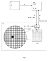
- Figure 1 shows a block schematic representing the system of the invention comprising a tester associated to a FPGA device connected to at least one chip of a wafer. Before personalization, the chip is set up in a test mode by secure data exchanges and verifications performed by the tester and the FPGA device.
- the system illustrated by figure 1 comprises a tester T associated to a FPGA device WB also called “waferbox" which configuration file is secured with known methods to prevent cloning.
- the test mode activation as well as the personalization process are preferably performed at wafer level i.e. the chips are arranged on a wafer used for their manufacturing.
- a hardware module HM preferably implemented on the wafer plays a role of interface between the FPGA device WB and the chips ICs on the wafer W and is in charge of verifying presence of the chip (s) ICs on the wafer W after initialization of the test mode. This verification prevents manipulations or attempt to modify personalization parameters when a chip is cut out of the wafer or integrated in a smart card in service in the field.
- the hardware module HM is destroyed at the end of personalization process during wafer cutting in order to separate all chips. Beside this physical security means, software and communication security means are also used to protect the sensitive personalization process. The combination of physical and software means prevents personalization by third parties owning only the necessary software programs without any link with a disposable physical hardware circuitry.
- the tester T is powered on as well as the FPGA device and the chip IC.
- the tester T reads and sends to the FPGA device WB a first secret code S1 which is retrieved from a permanent memory of the tester T.
- the FPGA device sends a command C to the chip IC which sends a signal s to the hardware module HM arranged on the wafer W.
- the hardware module HM returns a response r to the chip indicating its presence on the wafer i.e. not stand alone or integrated in a device connected to the FPGA device WB.
- the connection with the hardware module HM may be defective or the chip IC is detached from the wafer W.
- the tester T respectively the FPGA device WB in communication with the hardware module HM stops processing and an error message may be displayed.
- a status indicator ST (chip on the wafer /chip out of the wafer) may be reported to the FPGA device WB before continuation of the test mode sequence activation. This status indicator ST may be included in a response to the initialization command C.
- the chip IC After the successful communication with the hardware module HM, the chip IC generates a random number R and forwards it to the FPGA device WB.
- the random number R is preferably a true random i.e. produced with a hardware True Random Number Generator (TRNG) to improve statistical uniqueness of the result.
- TRNG hardware True Random Number Generator
- a first method is based on some physical phenomenon measurement (noise in semi-conductor elements for example) that is expected to be random and then compensates for possible biases in the measurement process.
- the second method uses computational algorithms that can produce long sequences of apparently random results, which are in fact completely determined by a shorter initial value, known as a seed or key.
- the latter type of generator is often called pseudo-random number generator.
- a "random number generator” based solely on deterministic computation cannot be regarded as a "true” random number generator, since its output is inherently predictable.
- Each data exchange between the FPGA device WB is statistically unique thanks to the true random number R used in the encryption /decryption algorithm E to calculate the cryptograms M1 and M2.
- the Boolean function F may be preferably a cryptographic one-way function such as a hash function of type SHA256 for example as described in document WO2010/130709A1 . Even the function F is known, it is quite impossible to recover the original value E -1 R, S1 (M1) from the resulting cryptogram M2.
- the FPGA device WB receives response message RES as OK or KO from the chip IC indicating that personalization steps can be executed or not.
- the first secret code S1 and the second secret code S2 constitute parts of a global secret code S.
- the first secret code S1 is stored in a permanent memory of the tester T and in a permanent memory of the chip IC and stored in a non permanent random access memory RAM of the FPGA device WB.
- the second secret code S2 is stored in a permanent memory of the FPGA device WB and stored in a non permanent random access memory RAM of the chip IC.
- the sharing of the secret code S by storing the secret codes S1 and S2 in the respective memories of the FPGA device and of the chip IC may be carried out at start of the tester T when connections of the system elements are initialized.
- the FPGA device WB is further configured to have access to encrypted non-volatile memory for loading application code in to the chip IC during the personalization phase.
- This memory may contain several versions of the application code so that the tester T respectively the FPGA device WB selects a predefined version of an application code stored in the memory of the chip (IC).
- the application code is sent by the FPGA device WB to the chip (IC) in a secure way by encryption using an algorithm depending on a true random number in a similar manner than in the process of test mode activation described above.
- the FPGA device WB is mechanically and electrically connected to the tester T in such a way to be physically inaccessible by users of the tester T during chip personalization phase. Furthermore the electronic modules composing the FPGA device WB are made tamper-proof or tamper-evident.
- the FPGA device WB transmits to the tester T information comprising its current state data and history data of the personalized chip IC for traceability purposes.
Landscapes
- Engineering & Computer Science (AREA)
- Computer Security & Cryptography (AREA)
- Theoretical Computer Science (AREA)
- Computer Hardware Design (AREA)
- General Engineering & Computer Science (AREA)
- Software Systems (AREA)
- Physics & Mathematics (AREA)
- General Physics & Mathematics (AREA)
- Computer Networks & Wireless Communication (AREA)
- Signal Processing (AREA)
- Microelectronics & Electronic Packaging (AREA)
- Mathematical Physics (AREA)
- Power Engineering (AREA)
- Semiconductor Integrated Circuits (AREA)
- Storage Device Security (AREA)
- Testing Or Measuring Of Semiconductors Or The Like (AREA)
Priority Applications (10)
| Application Number | Priority Date | Filing Date | Title |
|---|---|---|---|
| EP12188097.5A EP2720167A1 (fr) | 2012-10-11 | 2012-10-11 | Procédé et système de personnalisation de carte à puce de paiement |
| SG11201500972QA SG11201500972QA (en) | 2012-10-11 | 2013-10-08 | Method and system for smart card chip personalization |
| EP13773769.8A EP2907067B1 (fr) | 2012-10-11 | 2013-10-08 | Procédé et système de personnalisation de carte à puce de paiement |
| PCT/EP2013/070889 WO2014056876A1 (fr) | 2012-10-11 | 2013-10-08 | Procédé et système de personnalisation de puce de carte à puce |
| DK13773769.8T DK2907067T3 (en) | 2012-10-11 | 2013-10-08 | Smartcard chip personalization method and system |
| ES13773769.8T ES2619635T3 (es) | 2012-10-11 | 2013-10-08 | Método y sistema para personalización de chip de tarjeta inteligente |
| CN201380049538.5A CN104756123B (zh) | 2012-10-11 | 2013-10-08 | 用于智能卡芯片个性化的方法和系统 |
| PT137737698T PT2907067T (pt) | 2012-10-11 | 2013-10-08 | Método e sistema para personalização de chips para cartões inteligentes |
| US14/432,426 US9338004B2 (en) | 2012-10-11 | 2013-10-08 | Method and system for smart card chip personalization |
| US15/093,044 US9729322B2 (en) | 2012-10-11 | 2016-04-07 | Method and system for smart card chip personalization |
Applications Claiming Priority (1)
| Application Number | Priority Date | Filing Date | Title |
|---|---|---|---|
| EP12188097.5A EP2720167A1 (fr) | 2012-10-11 | 2012-10-11 | Procédé et système de personnalisation de carte à puce de paiement |
Publications (1)
| Publication Number | Publication Date |
|---|---|
| EP2720167A1 true EP2720167A1 (fr) | 2014-04-16 |
Family
ID=47010388
Family Applications (2)
| Application Number | Title | Priority Date | Filing Date |
|---|---|---|---|
| EP12188097.5A Withdrawn EP2720167A1 (fr) | 2012-10-11 | 2012-10-11 | Procédé et système de personnalisation de carte à puce de paiement |
| EP13773769.8A Active EP2907067B1 (fr) | 2012-10-11 | 2013-10-08 | Procédé et système de personnalisation de carte à puce de paiement |
Family Applications After (1)
| Application Number | Title | Priority Date | Filing Date |
|---|---|---|---|
| EP13773769.8A Active EP2907067B1 (fr) | 2012-10-11 | 2013-10-08 | Procédé et système de personnalisation de carte à puce de paiement |
Country Status (8)
| Country | Link |
|---|---|
| US (2) | US9338004B2 (fr) |
| EP (2) | EP2720167A1 (fr) |
| CN (1) | CN104756123B (fr) |
| DK (1) | DK2907067T3 (fr) |
| ES (1) | ES2619635T3 (fr) |
| PT (1) | PT2907067T (fr) |
| SG (1) | SG11201500972QA (fr) |
| WO (1) | WO2014056876A1 (fr) |
Cited By (3)
| Publication number | Priority date | Publication date | Assignee | Title |
|---|---|---|---|---|
| CN105045695A (zh) * | 2015-08-17 | 2015-11-11 | 大唐微电子技术有限公司 | 一种芯片进入测试模式的保护方法和系统 |
| CN108280372A (zh) * | 2018-02-23 | 2018-07-13 | 深圳国微技术有限公司 | 一种安全芯片 |
| CN110740306A (zh) * | 2019-10-24 | 2020-01-31 | 深圳市视特易智能科技有限公司 | 彩色相机白平衡统计校正模板及彩色白平衡统计校正方法 |
Families Citing this family (14)
| Publication number | Priority date | Publication date | Assignee | Title |
|---|---|---|---|---|
| US9900307B2 (en) * | 2014-02-27 | 2018-02-20 | Pinsheng Sun | Portable electronic card system and verifying method thereof |
| US9003109B1 (en) * | 2014-05-29 | 2015-04-07 | SanDisk Technologies, Inc. | System and method for distributed computing in non-volatile memory |
| EP3119031A1 (fr) * | 2015-07-16 | 2017-01-18 | ABB Schweiz AG | Schéma de chiffrement utilisant de multiples intervenants |
| CN106203066A (zh) * | 2016-08-03 | 2016-12-07 | 深圳中电长城信息安全系统有限公司 | 开机密码保护方法、终端及服务器 |
| EP3407181A1 (fr) * | 2017-05-23 | 2018-11-28 | Siemens Aktiengesellschaft | Procédé et dispositif de traitement assisté par ordinateur d'un profil binaire aléatoire |
| US20190197525A1 (en) * | 2017-12-21 | 2019-06-27 | Entrust Datacard Corporation | Secure end-to-end personalization of smart cards |
| CN109714163B (zh) * | 2019-01-30 | 2021-12-14 | 江永林 | 一种芯片序列号编码方法及系统、存储介质及终端 |
| SG11201908931TA (en) | 2019-03-29 | 2019-10-30 | Alibaba Group Holding Ltd | Cryptographic key management based on identity information |
| SG11201908930YA (en) | 2019-03-29 | 2019-10-30 | Alibaba Group Holding Ltd | Managing cryptographic keys based on identity information |
| AU2019204724C1 (en) * | 2019-03-29 | 2021-12-09 | Advanced New Technologies Co., Ltd. | Cryptography chip with identity verification |
| WO2019120323A2 (fr) | 2019-03-29 | 2019-06-27 | Alibaba Group Holding Limited | Exécution sécurisée d'opérations cryptographiques |
| CN111262697A (zh) * | 2020-01-16 | 2020-06-09 | 大唐微电子技术有限公司 | 一种芯片晶圆测试控制方法及装置、芯片 |
| CN111669865B (zh) * | 2020-07-03 | 2021-08-13 | 深圳爱克莱特科技股份有限公司 | 一种led智能控制系统硬件加密方法 |
| CN117056897B (zh) * | 2023-10-13 | 2023-12-26 | 沐曦集成电路(上海)有限公司 | 用于芯片验证的配置信息处理方法、电子设备和介质 |
Citations (4)
| Publication number | Priority date | Publication date | Assignee | Title |
|---|---|---|---|---|
| EP1441313A1 (fr) | 2003-01-24 | 2004-07-28 | France Telecom | Procédé cryptographique à clé publique pour la protection d' une puce électronique contre la fraude |
| WO2008057156A2 (fr) * | 2006-11-09 | 2008-05-15 | Broadon Communications Corp. | Procédé pour la programmation d'une mémoire non volatile sur puce dans un processeur sécurisé, et dispositif ainsi programmé |
| EP1983466A2 (fr) | 2007-04-17 | 2008-10-22 | Broadcom Corporation | Procédé et appareil d'authentification sécurisée pour système sur puce (SoC) |
| WO2010130709A1 (fr) | 2009-05-13 | 2010-11-18 | Nagravision S.A. | Procédé d'authentification d'accès à une puce sécurisée par un dispositif de test |
Family Cites Families (2)
| Publication number | Priority date | Publication date | Assignee | Title |
|---|---|---|---|---|
| CN101620656B (zh) * | 2009-07-29 | 2012-11-28 | 深圳国微技术有限公司 | 安全jtag电路及保护芯片内部信息安全的方法 |
| CN102332066B (zh) * | 2011-05-31 | 2014-09-24 | 贾松仁 | 跳码芯片识别码的认证管理系统及方法 |
-
2012
- 2012-10-11 EP EP12188097.5A patent/EP2720167A1/fr not_active Withdrawn
-
2013
- 2013-10-08 US US14/432,426 patent/US9338004B2/en not_active Expired - Fee Related
- 2013-10-08 WO PCT/EP2013/070889 patent/WO2014056876A1/fr active Application Filing
- 2013-10-08 CN CN201380049538.5A patent/CN104756123B/zh active Active
- 2013-10-08 DK DK13773769.8T patent/DK2907067T3/en active
- 2013-10-08 PT PT137737698T patent/PT2907067T/pt unknown
- 2013-10-08 SG SG11201500972QA patent/SG11201500972QA/en unknown
- 2013-10-08 ES ES13773769.8T patent/ES2619635T3/es active Active
- 2013-10-08 EP EP13773769.8A patent/EP2907067B1/fr active Active
-
2016
- 2016-04-07 US US15/093,044 patent/US9729322B2/en not_active Expired - Fee Related
Patent Citations (4)
| Publication number | Priority date | Publication date | Assignee | Title |
|---|---|---|---|---|
| EP1441313A1 (fr) | 2003-01-24 | 2004-07-28 | France Telecom | Procédé cryptographique à clé publique pour la protection d' une puce électronique contre la fraude |
| WO2008057156A2 (fr) * | 2006-11-09 | 2008-05-15 | Broadon Communications Corp. | Procédé pour la programmation d'une mémoire non volatile sur puce dans un processeur sécurisé, et dispositif ainsi programmé |
| EP1983466A2 (fr) | 2007-04-17 | 2008-10-22 | Broadcom Corporation | Procédé et appareil d'authentification sécurisée pour système sur puce (SoC) |
| WO2010130709A1 (fr) | 2009-05-13 | 2010-11-18 | Nagravision S.A. | Procédé d'authentification d'accès à une puce sécurisée par un dispositif de test |
Cited By (4)
| Publication number | Priority date | Publication date | Assignee | Title |
|---|---|---|---|---|
| CN105045695A (zh) * | 2015-08-17 | 2015-11-11 | 大唐微电子技术有限公司 | 一种芯片进入测试模式的保护方法和系统 |
| CN105045695B (zh) * | 2015-08-17 | 2018-08-10 | 大唐微电子技术有限公司 | 一种芯片进入测试模式的保护方法和系统 |
| CN108280372A (zh) * | 2018-02-23 | 2018-07-13 | 深圳国微技术有限公司 | 一种安全芯片 |
| CN110740306A (zh) * | 2019-10-24 | 2020-01-31 | 深圳市视特易智能科技有限公司 | 彩色相机白平衡统计校正模板及彩色白平衡统计校正方法 |
Also Published As
| Publication number | Publication date |
|---|---|
| CN104756123B (zh) | 2017-05-10 |
| WO2014056876A1 (fr) | 2014-04-17 |
| US20150270962A1 (en) | 2015-09-24 |
| DK2907067T3 (en) | 2017-05-01 |
| US9338004B2 (en) | 2016-05-10 |
| SG11201500972QA (en) | 2015-04-29 |
| CN104756123A (zh) | 2015-07-01 |
| US20160226662A1 (en) | 2016-08-04 |
| EP2907067A1 (fr) | 2015-08-19 |
| US9729322B2 (en) | 2017-08-08 |
| EP2907067B1 (fr) | 2017-01-11 |
| ES2619635T3 (es) | 2017-06-26 |
| PT2907067T (pt) | 2017-03-31 |
Similar Documents
| Publication | Publication Date | Title |
|---|---|---|
| US9729322B2 (en) | Method and system for smart card chip personalization | |
| KR101659110B1 (ko) | 테스트 디바이스에 의한 보안 칩으로의 액세스 인증 방법 | |
| EP1759338B1 (fr) | Systeme d'authentification à usage unique | |
| EP2506488B1 (fr) | Programmation de clé sur puce dynamique sécurisée | |
| CN106778205A (zh) | 运用物理不可克隆函数的无数据库验证 | |
| US20100250936A1 (en) | Integrated circuit, encryption communication apparatus, encryption communication system, information processing method and encryption communication method | |
| CN103415855A (zh) | 大容量存储设备存储器加密方法、系统及装置 | |
| CN103562922A (zh) | 在芯片制造期间建立唯一秘钥 | |
| JP2018500823A (ja) | 装置鍵保護 | |
| JP7087172B2 (ja) | Pqaロック解除 | |
| US20150012968A1 (en) | Information processing system | |
| EP2701101B1 (fr) | Dispositifs de traitement d'informations et procédés de traitement d'informations | |
| CN110046489B (zh) | 一种基于国产龙芯处理器的可信访问验证系统,计算机及可读存储介质 | |
| US11574079B2 (en) | Multi-stage provisioning of secret data | |
| US20110081016A1 (en) | Secure data communication using elliptic curve cryptology | |
| KR101350984B1 (ko) | 보안 토큰에 대한 발급자 인증 방법 및 그 장치 | |
| CN103178967A (zh) | 一种空白智能卡激活认证密钥方法及装置 |
Legal Events
| Date | Code | Title | Description |
|---|---|---|---|
| PUAI | Public reference made under article 153(3) epc to a published international application that has entered the european phase |
Free format text: ORIGINAL CODE: 0009012 |
|
| AK | Designated contracting states |
Kind code of ref document: A1 Designated state(s): AL AT BE BG CH CY CZ DE DK EE ES FI FR GB GR HR HU IE IS IT LI LT LU LV MC MK MT NL NO PL PT RO RS SE SI SK SM TR |
|
| AX | Request for extension of the european patent |
Extension state: BA ME |
|
| STAA | Information on the status of an ep patent application or granted ep patent |
Free format text: STATUS: THE APPLICATION IS DEEMED TO BE WITHDRAWN |
|
| 18D | Application deemed to be withdrawn |
Effective date: 20141017 |