EP2717548A1 - Portable electronic device, group of portable electronic devices, and method for manufacturing portable electronic device - Google Patents
Portable electronic device, group of portable electronic devices, and method for manufacturing portable electronic device Download PDFInfo
- Publication number
- EP2717548A1 EP2717548A1 EP12793060.0A EP12793060A EP2717548A1 EP 2717548 A1 EP2717548 A1 EP 2717548A1 EP 12793060 A EP12793060 A EP 12793060A EP 2717548 A1 EP2717548 A1 EP 2717548A1
- Authority
- EP
- European Patent Office
- Prior art keywords
- electronic device
- circuit board
- housing
- antenna
- board
- Prior art date
- Legal status (The legal status is an assumption and is not a legal conclusion. Google has not performed a legal analysis and makes no representation as to the accuracy of the status listed.)
- Granted
Links
Images






Classifications
-
- H—ELECTRICITY
- H04—ELECTRIC COMMUNICATION TECHNIQUE
- H04M—TELEPHONIC COMMUNICATION
- H04M1/00—Substation equipment, e.g. for use by subscribers
- H04M1/02—Constructional features of telephone sets
- H04M1/0202—Portable telephone sets, e.g. cordless phones, mobile phones or bar type handsets
- H04M1/026—Details of the structure or mounting of specific components
-
- G—PHYSICS
- G06—COMPUTING OR CALCULATING; COUNTING
- G06F—ELECTRIC DIGITAL DATA PROCESSING
- G06F1/00—Details not covered by groups G06F3/00 - G06F13/00 and G06F21/00
- G06F1/16—Constructional details or arrangements
- G06F1/1613—Constructional details or arrangements for portable computers
- G06F1/1633—Constructional details or arrangements of portable computers not specific to the type of enclosures covered by groups G06F1/1615 - G06F1/1626
- G06F1/1684—Constructional details or arrangements related to integrated I/O peripherals not covered by groups G06F1/1635 - G06F1/1675
- G06F1/1698—Constructional details or arrangements related to integrated I/O peripherals not covered by groups G06F1/1635 - G06F1/1675 the I/O peripheral being a sending/receiving arrangement to establish a cordless communication link, e.g. radio or infrared link, integrated cellular phone
-
- A—HUMAN NECESSITIES
- A63—SPORTS; GAMES; AMUSEMENTS
- A63F—CARD, BOARD, OR ROULETTE GAMES; INDOOR GAMES USING SMALL MOVING PLAYING BODIES; VIDEO GAMES; GAMES NOT OTHERWISE PROVIDED FOR
- A63F13/00—Video games, i.e. games using an electronically generated display having two or more dimensions
- A63F13/20—Input arrangements for video game devices
- A63F13/21—Input arrangements for video game devices characterised by their sensors, purposes or types
- A63F13/214—Input arrangements for video game devices characterised by their sensors, purposes or types for locating contacts on a surface, e.g. floor mats or touch pads
-
- A—HUMAN NECESSITIES
- A63—SPORTS; GAMES; AMUSEMENTS
- A63F—CARD, BOARD, OR ROULETTE GAMES; INDOOR GAMES USING SMALL MOVING PLAYING BODIES; VIDEO GAMES; GAMES NOT OTHERWISE PROVIDED FOR
- A63F13/00—Video games, i.e. games using an electronically generated display having two or more dimensions
- A63F13/20—Input arrangements for video game devices
- A63F13/21—Input arrangements for video game devices characterised by their sensors, purposes or types
- A63F13/214—Input arrangements for video game devices characterised by their sensors, purposes or types for locating contacts on a surface, e.g. floor mats or touch pads
- A63F13/2145—Input arrangements for video game devices characterised by their sensors, purposes or types for locating contacts on a surface, e.g. floor mats or touch pads the surface being also a display device, e.g. touch screens
-
- A—HUMAN NECESSITIES
- A63—SPORTS; GAMES; AMUSEMENTS
- A63F—CARD, BOARD, OR ROULETTE GAMES; INDOOR GAMES USING SMALL MOVING PLAYING BODIES; VIDEO GAMES; GAMES NOT OTHERWISE PROVIDED FOR
- A63F13/00—Video games, i.e. games using an electronically generated display having two or more dimensions
- A63F13/20—Input arrangements for video game devices
- A63F13/24—Constructional details thereof, e.g. game controllers with detachable joystick handles
-
- A—HUMAN NECESSITIES
- A63—SPORTS; GAMES; AMUSEMENTS
- A63F—CARD, BOARD, OR ROULETTE GAMES; INDOOR GAMES USING SMALL MOVING PLAYING BODIES; VIDEO GAMES; GAMES NOT OTHERWISE PROVIDED FOR
- A63F13/00—Video games, i.e. games using an electronically generated display having two or more dimensions
- A63F13/90—Constructional details or arrangements of video game devices not provided for in groups A63F13/20 or A63F13/25, e.g. housing, wiring, connections or cabinets
-
- A—HUMAN NECESSITIES
- A63—SPORTS; GAMES; AMUSEMENTS
- A63F—CARD, BOARD, OR ROULETTE GAMES; INDOOR GAMES USING SMALL MOVING PLAYING BODIES; VIDEO GAMES; GAMES NOT OTHERWISE PROVIDED FOR
- A63F13/00—Video games, i.e. games using an electronically generated display having two or more dimensions
- A63F13/90—Constructional details or arrangements of video game devices not provided for in groups A63F13/20 or A63F13/25, e.g. housing, wiring, connections or cabinets
- A63F13/92—Video game devices specially adapted to be hand-held while playing
-
- G—PHYSICS
- G06—COMPUTING OR CALCULATING; COUNTING
- G06F—ELECTRIC DIGITAL DATA PROCESSING
- G06F1/00—Details not covered by groups G06F3/00 - G06F13/00 and G06F21/00
- G06F1/16—Constructional details or arrangements
- G06F1/1613—Constructional details or arrangements for portable computers
- G06F1/1633—Constructional details or arrangements of portable computers not specific to the type of enclosures covered by groups G06F1/1615 - G06F1/1626
- G06F1/1656—Details related to functional adaptations of the enclosure, e.g. to provide protection against EMI, shock, water, or to host detachable peripherals like a mouse or removable expansions units like PCMCIA cards, or to provide access to internal components for maintenance or to removable storage supports like CDs or DVDs, or to mechanically mount accessories
- G06F1/1658—Details related to functional adaptations of the enclosure, e.g. to provide protection against EMI, shock, water, or to host detachable peripherals like a mouse or removable expansions units like PCMCIA cards, or to provide access to internal components for maintenance or to removable storage supports like CDs or DVDs, or to mechanically mount accessories related to the mounting of internal components, e.g. disc drive or any other functional module
-
- A—HUMAN NECESSITIES
- A63—SPORTS; GAMES; AMUSEMENTS
- A63F—CARD, BOARD, OR ROULETTE GAMES; INDOOR GAMES USING SMALL MOVING PLAYING BODIES; VIDEO GAMES; GAMES NOT OTHERWISE PROVIDED FOR
- A63F2300/00—Features of games using an electronically generated display having two or more dimensions, e.g. on a television screen, showing representations related to the game
- A63F2300/10—Features of games using an electronically generated display having two or more dimensions, e.g. on a television screen, showing representations related to the game characterized by input arrangements for converting player-generated signals into game device control signals
- A63F2300/1043—Features of games using an electronically generated display having two or more dimensions, e.g. on a television screen, showing representations related to the game characterized by input arrangements for converting player-generated signals into game device control signals being characterized by constructional details
-
- A—HUMAN NECESSITIES
- A63—SPORTS; GAMES; AMUSEMENTS
- A63F—CARD, BOARD, OR ROULETTE GAMES; INDOOR GAMES USING SMALL MOVING PLAYING BODIES; VIDEO GAMES; GAMES NOT OTHERWISE PROVIDED FOR
- A63F2300/00—Features of games using an electronically generated display having two or more dimensions, e.g. on a television screen, showing representations related to the game
- A63F2300/10—Features of games using an electronically generated display having two or more dimensions, e.g. on a television screen, showing representations related to the game characterized by input arrangements for converting player-generated signals into game device control signals
- A63F2300/1068—Features of games using an electronically generated display having two or more dimensions, e.g. on a television screen, showing representations related to the game characterized by input arrangements for converting player-generated signals into game device control signals being specially adapted to detect the point of contact of the player on a surface, e.g. floor mat, touch pad
-
- A—HUMAN NECESSITIES
- A63—SPORTS; GAMES; AMUSEMENTS
- A63F—CARD, BOARD, OR ROULETTE GAMES; INDOOR GAMES USING SMALL MOVING PLAYING BODIES; VIDEO GAMES; GAMES NOT OTHERWISE PROVIDED FOR
- A63F2300/00—Features of games using an electronically generated display having two or more dimensions, e.g. on a television screen, showing representations related to the game
- A63F2300/10—Features of games using an electronically generated display having two or more dimensions, e.g. on a television screen, showing representations related to the game characterized by input arrangements for converting player-generated signals into game device control signals
- A63F2300/1068—Features of games using an electronically generated display having two or more dimensions, e.g. on a television screen, showing representations related to the game characterized by input arrangements for converting player-generated signals into game device control signals being specially adapted to detect the point of contact of the player on a surface, e.g. floor mat, touch pad
- A63F2300/1075—Features of games using an electronically generated display having two or more dimensions, e.g. on a television screen, showing representations related to the game characterized by input arrangements for converting player-generated signals into game device control signals being specially adapted to detect the point of contact of the player on a surface, e.g. floor mat, touch pad using a touch screen
-
- A—HUMAN NECESSITIES
- A63—SPORTS; GAMES; AMUSEMENTS
- A63F—CARD, BOARD, OR ROULETTE GAMES; INDOOR GAMES USING SMALL MOVING PLAYING BODIES; VIDEO GAMES; GAMES NOT OTHERWISE PROVIDED FOR
- A63F2300/00—Features of games using an electronically generated display having two or more dimensions, e.g. on a television screen, showing representations related to the game
- A63F2300/20—Features of games using an electronically generated display having two or more dimensions, e.g. on a television screen, showing representations related to the game characterised by details of the game platform
- A63F2300/204—Features of games using an electronically generated display having two or more dimensions, e.g. on a television screen, showing representations related to the game characterised by details of the game platform the platform being a handheld device
-
- H—ELECTRICITY
- H04—ELECTRIC COMMUNICATION TECHNIQUE
- H04M—TELEPHONIC COMMUNICATION
- H04M2250/00—Details of telephonic subscriber devices
- H04M2250/22—Details of telephonic subscriber devices including a touch pad, a touch sensor or a touch detector
-
- H—ELECTRICITY
- H05—ELECTRIC TECHNIQUES NOT OTHERWISE PROVIDED FOR
- H05K—PRINTED CIRCUITS; CASINGS OR CONSTRUCTIONAL DETAILS OF ELECTRIC APPARATUS; MANUFACTURE OF ASSEMBLAGES OF ELECTRICAL COMPONENTS
- H05K1/00—Printed circuits
- H05K1/02—Details
- H05K1/14—Structural association of two or more printed circuits
-
- H—ELECTRICITY
- H05—ELECTRIC TECHNIQUES NOT OTHERWISE PROVIDED FOR
- H05K—PRINTED CIRCUITS; CASINGS OR CONSTRUCTIONAL DETAILS OF ELECTRIC APPARATUS; MANUFACTURE OF ASSEMBLAGES OF ELECTRICAL COMPONENTS
- H05K1/00—Printed circuits
- H05K1/18—Printed circuits structurally associated with non-printed electric components
Definitions
- FIG. 1 is a front view of a portable type electronic device 10 according to an embodiment of the present invention.
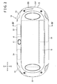
- FIG. 2 is a rear view of the electronic device 10.
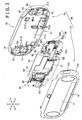
- FIG. 3 is an exploded perspective view of the electronic device 10.
- FIG. 4 is a sectional view of a housing, the section being taken along a line IV-IV shown in FIG. 2 .
- directions denoted by X1 and X2 in FIG. 1 are a left direction and a right direction, respectively, and directions denoted by Z1 and Z2 in FIG. 1 are an upward direction and a downward direction, respectively.
- directions denoted by Y1 and Y2 in FIG. 4 are a front direction and a rear direction, respectively.
- the display panel unit 2 in the present example has a touch panel 2b.
- the touch panel 2b is a position detecting device for detecting the position of a finger of a user when the user touches the front surface (surface of the front panel 22 in the present example) of the electronic device 10 with the finger.
- the touch panel 2b in the present example is a capacitive type panel.
- the touch panel 2b is not limited to this. Panels of other types such as a resistive film type, an electromagnetic induction type, and the like may be used as the touch panel 2b.
- the electronic device 10 in the present example is a device that functions as a game device and a moving image and audio reproducing device. As shown in FIG 1 , the electronic device 10 has a plurality of operating members operated by the user during game play or the like on the left and right of the display panel unit 2. In the present example, a plurality of operating buttons (four operating buttons in the present example) 5 are disposed on the right side of the display panel unit 2. The four buttons 5 are located at respective end portions of a cross. In addition, a cross key 6 is disposed on the left side of the display panel unit 2. Further, operating sticks 7 and 8 are disposed respectively on the right side and the left side of the display panel unit 2.
- the plurality of operating members 5, 6, 7, and 8 are disposed so as to project forward from openings 22a and 22b formed in the front panel 22.
- the front housing main body 21 has a plate-shaped frame portion 21c that is located on the inside of the peripheral wall portion 21b and which covers the front side of the circuit board 40.
- the frame portion 21c retains a base 5a that is disposed on the back surface side of the plurality of operating buttons 5 and which supports the operating buttons 5 in such a manner as to be movable forward and rearward and a base 6 that is disposed on the back surface side of the cross key 6 and which supports the end portions of the cross key 6 in such a manner as to be movable forward and rearward.
- the frame portion 21c retains cases 7c and 8c of supporting mechanisms that are located at base portions of the operating sticks 7 and 8 and which support the base portions of the operating sticks 7 and 8.
- FIG. 7 is a perspective view of the first antenna 31.
- the first antenna 31 has a base 31a formed by resin.
- the base 31a has a box shape opened to the front.
- the first antenna 31 has the film-shaped antenna main body 31b.
- the antenna main body 31b is laminated to the outer surface (rear surface) of the base 31a, and faces the rear.
- ribs 31c for securing the strength of the base 31a are formed on the inside of the base 31a.
- pawl-shaped engaging portions 31d are formed on the left and right of the base 31a. The engaging portions 31d catch on the wall portions defining the first housing space 23a. The first antenna 31 is thereby fixed to the back housing 23.
- the electronic device 10 includes the third antenna 33 and the fourth antenna 34.
- the third antenna 33 and the fourth antenna 34 are disposed on the opposite side from the first antenna 31 with the rear touch panel 4 interposed in between. According to this layout, a sufficient distance is secured from the first antenna 31 to the third antenna 33 and the fourth antenna 34. As a result, good reception sensitivity of these antennas is obtained easily.
- the battery 9 is disposed between the first antenna 31 and the third antenna 33 and the fourth antenna 34.
- the third antenna 33 and the fourth antenna 34 are disposed on the opposite sides from each other with the center C in the left-right direction of the display panel unit 2 interposed in between, and a camera unit 11 is disposed between the third antenna 33 and the fourth antenna 34. According to such a layout, a space between the third antenna 33 and the fourth antenna 34 can be used effectively while a sufficient distance is secured between the third antenna 33 and the fourth antenna 34.
- the antennas 32, 33, and 34 respectively have film-shaped antenna main bodies 32b, 33b, and 34b.
- the antenna main bodies 32b, 33b, and 34b are laminated to the outer surfaces (rear surfaces) of the bases 32a, 33a, and 34a, and face the rear.
- the back housing 23 in the present example has the curved outer peripheral portion 23f.
- the base 32a and the antenna main body 32b of the second antenna 32 are curved along the outer peripheral portion 23f. According to such a shape of the antenna main body 32b, as with the antenna main body 31b, the antenna main body 32b can have a width in the front-rear direction, and thus obtain good reception sensitivity.
- the base 33a and the antenna main body 33b of the third antenna 33 and the base 34a and the antenna main body 34b of the fourth antenna 34 are also curved along the outer peripheral portion 23f.
- the electronic device 10 includes the first antenna 31, the second antenna 32, and the third antenna 33.
- the communication module 50 is a module in charge of processing for communications, such for example as demodulation processing/modulation processing on signals received/to be transmitted by the antennas 31 to 33.
- the communication module 50 in the present example is disposed on the back surface side of the main board 41. As shown in FIG. 10 , the communication module 50 has a circuit board (hereinafter referred to as a module board) 51 smaller than the main board 41.
- the module board 51 is disposed in such an attitude as to face the main board 41.
- the connector 55 has an insertion slot 55a for receiving the upper edge of the module board 51.
- the insertion slot 55a is located so as to be separated from the surface of the main board 41.
- a left and a right base 59 projecting in a direction of thickness of the main board 41 are formed on the main board 41.
- a lower edge of the module board 51 is attached to the bases 59 by screws 59a.
- the communication module 50 is supported in a state of being separated from the main board 41 by such an attachment structure.
- the retaining portion 71 is located on the shield plate 53, and is thus located at a higher position than the connectors 51b and 51c.
- the position in the upward-downward direction and the left-right direction of the cable holder 70 is defined by the shield plate 53.
- a plurality of projections (four projections in the present example) 73 surrounding the outer periphery of the shield plate 53 as a whole are formed on the cable holder 70.
- the positions of the projections 73 correspond to four corner portions of the shield plate 53.
- Each of the projections 73 is bent so as to surround the outside of the corner portion of the shield plate 53.
- the shield plate 53 is disposed on the inside of the four projections 73.
- the cable 61 extends from the module board 51 to the opposite side from the above-described cables 62 and 63 (see FIG. 9 ).
- the cable holder 70 has a guide portion 76 in a lower portion of the cable holder 70, the guide portion 76 defining the position of the cable 61 in a region on the outside of an outer edge of the module board 51. That is, the guide portion 76 forms side walls of a passage F1 in which the cable 61 is disposed.
- the guide portion 76 forms the passage F1 extending in one of the left direction and the right direction.
- the passage F1 in the present example extends in the right direction while bending at a plurality of positions.
- a microprocessor (not shown) that controls the whole of the electronic device 10 and which performs image processing is mounted on the main board 41.
- a connector (not shown) into which a terminal of a cable for connecting an external device to the electronic device 10 is inserted is also attached to the main board 41.
- the main board 41 is located on the back surface side of the above-described display panel unit 2 (see FIG. 1 ).
- the electronic device 10 has flat metallic plates 81, 82, and 83.
- the metallic plates 81, 82, and 83 are for example members formed by press working from one metallic plate.
- the metallic plate 81 is attached to the surface of the main board 41 and the surface of the right sub-board 42.
- a ground pattern is formed on the surface of the main board 41 and on the surface of the right sub-board 42. These ground patterns are connected to each other by the metallic plate 81.
- the metallic plates 82 and 83 are attached to the surface of the main board 41 and the surface of the left sub-board 43.
- a ground pattern is also formed on the surface of the left sub-board 43.
- bosses 21d having screw holes formed therein into which screw holes the screws 81a, 81b, 82a, 82b, 83a, and 83b are screwed are formed on the frame portion 21c of the front housing 24 (see FIG. 3 ).
- the screws 81a and 81b press the metallic plate 81 and the boards 41 and 42 against the bosses 21d.
- the screws 82a, 82b, 83a, and 83b press the metallic plates 82 and 83 and the boards 41 and 43 against the bosses 21d.
- This structure can further increase the contact pressure between the metallic plates 81, 82, and 83 and the ground patterns of the boards 41, 42, and 43.
- the board 56a is disposed in such an attitude as to face the circuit board 40 (left sub-board 43 in the present example), and is connected to the circuit board 40 (main board 41 in the present example) through a flat cable.
- the receiving plate 56b functions as a mount for mounting the IC card, and is slidable to the outside of the electronic device 10 (in the left direction in the present example) with respect to the board 56a. The user places the IC card on the receiving plate 56b, and slides the receiving plate 56b to the board 56a.
- the communication module 50 has the module board 51 separate from the main board 41.
- the module board 51 is attached to the main board 41 by the screws 59a (see FIG. 10 ).
- a circuit pattern for functions common to the electronic device 10 and the electronic device 110 is formed on the main board 41 easily as compared with a structure in which the IC chips possessed by the communication module 50 is soldered directly to the main board 41.
- the rear touch panel 4 is offset upward with respect to the display panel 2a, and the first antenna 31 is located downward with respect to the rear touch panel 4. According to this layout, an antenna having a large width in the upward-downward direction can be used as the first antenna 31.
- the first antenna 31 is disposed so as to be offset downward from the rear touch panel 4, and the second antenna 32 is disposed so as to be offset in the right direction from the rear touch panel 4. According to this layout, the possibility of both of the first antenna 31 and the second antenna 32 being covered by the hands of the user can be reduced.
- the position of the battery 9 is offset in the left direction with respect to the center C in the left-right direction of the housing 20. According to this layout, when the user holds the electronic device 10 with one hand, the user often holds the left side part of the electronic device 10 in which the battery 9 is disposed. The second antenna 32 is not covered by the hand when the user holds the left side part of the electronic device 10. Thus, good reception sensitivity can be obtained.
- the third antenna 33 and the fourth antenna 34 are disposed on the opposite side from the first antenna 31 with the rear touch panel 4 interposed in between. According to this layout, the distance between these antennas can be increased. Thus, good reception sensitivity is obtained easily.
- the first antenna 31 may be disposed closer to the display panel 2a than to the rear touch panel 4, and disposed so as to be offset from the display panel 2a so that at least a part of the first antenna 31 does not overlap the display panel 2a in the front-rear direction.
- the size of the display panel 2a may be smaller than the size of the rear touch panel 4.
- the cable holder 70 has the two engaging portions 72 engaged with the outer edges of the module board 51. According to this structure, the cable holder 70 can be attached to the module board 51 easily.
- the ground pattern of the main board 41 and the ground pattern of the right sub-board 42 are connected to each other by the metallic plate 81, and the ground pattern of the main board 41 and the ground pattern of the left sub-board 43 are connected to each other by the metallic plates 82 and 83. According to this structure, ground impedance can be lowered while a plurality of circuit boards are used.
- the present invention is not limited to the electronic device 10 described above, but various changes may be made.
- the circuit board 40 includes the main board 41, the right sub-board 42, and the left sub-board 43.
- the circuit board 40 may be formed by the main board 41 and the right sub-board 42 or by the main board 41 and the left sub-board 43.
- the flat cables 84 and 85 include the bent lines 84a and 85a.
- the flat cables 84 and 85 do not necessarily need to include the bent lines 84a and 85a.
- the communication module 50 has the module board 51 separate from the circuit board 40. According to this structure, a circuit pattern for functions common to the electronic device 10 and the electronic device 110 is formed on the circuit board 40 easily as compared with a structure in which the IC chips possessed by the communication module 50 is soldered directly to the circuit board 40.
- the receiving device 56 has the circuit board 56a separate from the circuit board 40. According to this structure, a circuit pattern for functions common to the electronic device 10 and the electronic device 110 is formed on the circuit board 40 easily as compared with a structure in which an IC chip slot is soldered directly to the circuit board 40.
- the antennas 31 and 32 of the electronic device 10 include the bases 31a and 32a formed of resin.
- the back housing 123 of the electronic device 110 has the ribs 123a and 123b formed of resin as a structure for reinforcing the back housing 123. According to this structure, a difference between the weight of the electronic device 10 and the weight of the electronic device 110 can be reduced.
- a plurality of parts for the additional communicating function which parts are not included in the electronic device 110 are disposed between the back housing 23 and the circuit board 40 of the electronic device 10. Then, a housing common to the front housing 24 of the electronic device 110 is used as the front housing 24 of the electronic device 10. According to this manufacturing method, the front housing 24 is common in the electronic device 10 and the electronic device 110. Thus the manufacturing cost of these two electronic devices can be reduced.
- the electronic device group including the electronic device 10 and the electronic device 110 is susceptible of various changes.
- the electronic device 10 includes the antennas 31 and 32, the communication module 50, and the receiving device 56 as a plurality of parts not included in the electronic device 110.
- the plurality of parts are not limited to these parts. Another part may not be included in the electronic device 110.
Landscapes
- Engineering & Computer Science (AREA)
- Multimedia (AREA)
- Human Computer Interaction (AREA)
- Computer Hardware Design (AREA)
- General Engineering & Computer Science (AREA)
- Theoretical Computer Science (AREA)
- Physics & Mathematics (AREA)
- General Physics & Mathematics (AREA)
- Signal Processing (AREA)
- Telephone Set Structure (AREA)
- Support Of Aerials (AREA)
Abstract
Description
- The present invention relates to a portable type electronic device, a portable type electronic device group, and a method of manufacturing the portable type electronic device.
-
- (1) Conventionally, portable type electronic devices capable of wireless communication using a mobile telephone network and wireless communication using a wireless LAN have been used. Electronic devices of this type include an antenna (see for example
US 2007/0,202,956 A1 ). - (2) In addition, inside a portable type electronic device, an IC chip mounted on a circuit board and other electronic parts included in the electronic device may be connected to each other via a cable.
- (3) In addition, as disclosed in
US 2007/0,202,956 A1 , portable type electronic devices having a wireless communication function have been conventionally used. The frequencies of radio waves used in wireless communication have recently been increased. It is desired that electronic devices handling high-frequency signals have a large ground, and that the impedance thereof be low. A conventional portable type electronic device has one circuit board coinciding substantially in size with a housing, and a ground layer is formed in the circuit board. According to such a structure, a large and low-impedance ground can be obtained. - (4) Further, an electronic device of
US 2007/0,202,956 A1 has a display screen in a front surface, and has operating members that can be operated by a user on the left and right of the display screen. - This electronic device has a communicating function using a wireless LAN.
-
- (1) The applicant is considering a portable type electronic device having a display panel in a front surface and having a touch panel in a rear surface. A large distance between such panels and an antenna is desirable for reception sensitivity of the antenna. In a mode of the present invention, a portable type electronic device includes: a housing; a display panel disposed on a front surface side of the housing; a rear touch panel disposed on a back surface side of the housing; and an antenna housed in the housing. The antenna is disposed closer to the other panel from one panel of the display panel and the rear touch panel in a front-rear direction of the housing, and the antenna is located so as to be offset from the other panel in a direction perpendicular to the front-rear direction of the housing so that at least a part of the antenna does not overlap the other panel in the front-rear direction of the housing. According to this electronic device, both of an adverse effect from the display panel and an adverse effect from the rear touch panel on the reception sensitivity of the antenna can be reduced.
- (2) For the miniaturization of the electronic device, a cable need to be disposed while a space within the electronic device is used effectively. However, because the cable usually has a surplus length, the position of the cable is not easily fixed within the electronic device. Therefore, when the cable is disposed in a narrow space within the electronic device, the cable and other parts tend to interfere with each other. In a mode of the present invention, an electronic device includes: a circuit board; an electronic part disposed on the circuit board; a cable disposed so as to straddle the electronic part; and a cable holder attached to the circuit board, the cable holder including a retaining portion for retaining the cable, the retaining portion being located on an opposite side of the electronic part from the circuit board. According to this electronic device, interference with other parts provided to the electronic device can be prevented while a space over the electronic part is used.
- (3) When one circuit board coinciding in size with the housing in the electronic device is used, the following inconvenience may arise. For example, the number of layers possessed by a circuit board has recently been increasing with increase in multifunctionality of the electronic device. However, while a region in which a CPU and a GPU are mounted needs many layers, a relatively small number of layers may suffice for other regions. In addition, because an external force tends to act on a part of the circuit board, only that part may need to have a high strength. When the whole of one circuit board coinciding in size with the housing has multiple layers or a high-strength material is used for the whole of one circuit board in these cases, an inconvenience of an increase in cost and weight arises. In a mode of the present invention, a portable type electronic device includes: a first circuit board having a ground pattern on a surface; a second circuit board having a ground pattern on a surface, disposed so as to be adjacent to the first circuit board, and connected to the first circuit board through a cable including a signal line; and a metallic plate attached to the surface of the first circuit board and the surface of the second circuit board to electrically connect the ground patterns of the two boards to each other. According to this electronic device, ground impedance can be lowered while the plurality of circuit boards are used.
- (4) Recently, portable type electronic devices having not only a communicating function using a wireless LAN but also a communicating function using a mobile telephone network have spread. However, while there are users who need these two communicating functions, there are users who need only the wireless LAN communicating function and consider the communicating function using the mobile telephone network to be unnecessary. In order to meet such demands of the users, the applicant is considering two kinds of portable type electronic devices that have a difference only in communicating functions and to which the arrangement, external shapes, and the like of operating members are common. However, when there are many parts not common to the two kinds of electronic devices in a case where such portable type electronic devices are manufactured, manufacturing cost thereof is increased.
- (4-1) In a mode of the present invention, an electronic device includes: a circuit board; and a housing including a front housing covering a front side of the circuit board and provided with a display screen and an operating member and a back housing covering a back surface side of the circuit board. In addition, the electronic device includes: an antenna housed in the housing; a communication module housed in the housing and transmitting and receiving a signal through the antenna; and a receiving device housed in the housing, the receiving device receiving an IC card used for communication by the antenna and the communication module. The antenna, the communication module, and the receiving device are disposed between the back housing and the circuit board. According to this mode, the front housing can be made common in the portable type electronic device including the antenna, the communication module, and the receiving device and a portable type electronic device not including these parts, and thus manufacturing cost of these portable type electronic devices can be reduced.
- (4-2) A portable type electronic device group according to a mode of the present invention includes a first portable type electronic device including a circuit board, a front housing covering a front side of the circuit board and provided with a display screen and an operating member, and a back housing covering a back side of the circuit board. The electronic device group also includes a second portable type electronic device including a circuit board, a front housing covering a front side of the circuit board and provided with a display screen and an operating member, and a back housing covering a back side of the circuit board, the second portable type electronic device not having a part of functions provided to the first portable type electronic device. The first electronic device has a plurality of parts for the part of the functions, the plurality of parts not being included in the second electronic device, and the plurality of parts are disposed between the back housing and the circuit board in the first electronic device. A structure of the front housing of the first electronic device and a structure of the front housing of the second electronic device are common to each other. According to this mode, the structure of the front housing is common in the first electronic device and the second electronic device. Thus, the manufacturing cost of these two electronic devices can be reduced.
- (4-3) A manufacturing method according to a mode of the present invention is a method of manufacturing: a first portable type electronic device including a circuit board, a front housing covering a front side of the circuit board and provided with a display screen and an operating member, and a back housing covering a back side of the circuit board; and a second portable type electronic device including a circuit board, a front housing covering a front side of the circuit board and provided with a display screen and an operating member, and a back housing covering a back side of the circuit board, the second portable type electronic device not having a part of functions provided to the first electronic device. In this manufacturing method, a plurality of parts for the part of the functions, the plurality of parts not being included in the second electronic device, are disposed between the back housing and the circuit board in the first electronic device, and a housing common to the front housing of the second electronic device is used as the front housing of the first electronic device. According to this manufacturing method, the front housing is common in the first portable type electronic device and the second portable type electronic device. Thus, the manufacturing cost of these two electronic devices can be reduced.
-
- [
FIG. 1 ]
FIG. 1 is a front view of a portable type electronic device according to an embodiment of the present invention. - [
FIG. 2 ]
FIG. 2 is a rear view of the electronic device. - [
FIG. 3 ]
FIG. 3 is an exploded perspective view of the electronic device. - [
FIG. 4 ]
FIG. 4 is a sectional view of a housing, the section being taken along a line IV-IV shown inFIG. 2 . - [
FIG. 5 ]
FIG. 5 is a diagram showing the layout of antennas provided to the electronic device. - [
FIG. 6 ]
FIG. 6 is an exploded perspective view of a back housing and the antennas. - [
FIG. 7 ]
FIG. 7 is a perspective view of the first antenna shown inFIG. 5 . - [
FIG. 8 ]
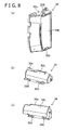
FIG. 8 is a perspective view of the second antenna, the third antenna, and the fourth antenna shown inFIG. 5 . - [
FIG. 9 ]
FIG. 9 is a rear view of a circuit board provided to the electronic device. - [
FIG. 10 ]
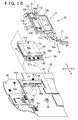
FIG. 10 is an exploded perspective view of a communication module and a cable holder provided to the circuit board shown inFIG. 9 . - [
FIG. 11 ]
FIG. 11 is a perspective view of the cable holder. - [
FIG. 12 ]
FIG. 12 is a rear view of the whole of the circuit board. - [
FIG. 13 ]
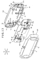
FIG. 13 is an exploded perspective view of another portable type electronic device than the electronic device shown inFIGS. 1 to 12 . The electronic device shown inFIG. 13 has common functions with the electronic device shown inFIGS. 1 to 12 other than a communicating function using a mobile telephone network among the functions possessed by the electronic device shown inFIGS. 1 to 12 . - [
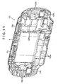
FIG. 14 ]
FIG. 14 is a perspective view of the inside of a back housing of the electronic device shown inFIG. 13 . - An embodiment of the present invention will hereinafter be described with reference to the drawings.
FIG. 1 is a front view of a portable typeelectronic device 10 according to an embodiment of the present invention.FIG. 2 is a rear view of theelectronic device 10.FIG. 3 is an exploded perspective view of theelectronic device 10.FIG. 4 is a sectional view of a housing, the section being taken along a line IV-IV shown inFIG. 2 . - Incidentally, the following description, directions denoted by X1 and X2 in
FIG. 1 are a left direction and a right direction, respectively, and directions denoted by Z1 and Z2 inFIG. 1 are an upward direction and a downward direction, respectively. In addition, directions denoted by Y1 and Y2 inFIG. 4 are a front direction and a rear direction, respectively. - The
electronic device 10 has ahousing 20 that houses acircuit board 40 and the like and which forms an external surface of theelectronic device 10. As shown inFIG. 3 , thehousing 20 in the present example is formed by afront housing 24 covering the front side of thecircuit board 40 and aback housing 23 that covers the back side of thecircuit board 40 and which is combined with thefront housing 24 in a front-rear direction. As shown inFIG. 4 , thefront housing 24 is formed by a front housingmain body 21 and afront panel 22 that is disposed on the front side of the front housingmain body 21 and which forms a front surface of theelectronic device 10. Thefront panel 22 is attached to the front housingmain body 21. The front housingmain body 21 has aperipheral wall portion 21b forming side surfaces, an upper surface, and a lower surface of theelectronic device 10. An outer peripheral portion of thefront panel 22 is attached to an edge of theperipheral wall portion 21b. Thefront panel 22 is formed of an optically transparent material (for example glass or resin such as an acrylic or the like). The front housingmain body 21 and theback housing 23 are also molded of a resin. - As shown in
FIG. 1 andFIG. 4 , theelectronic device 10 has adisplay panel unit 2 including adisplay panel 2a on the front surface side of thehousing 20, that is, on thefront panel 22. Various display panels such for example as a liquid crystal display panel, an organic EL panel, or a field emission display panel can be used as thedisplay panel 2a. - In addition, the
display panel unit 2 in the present example has atouch panel 2b. Thetouch panel 2b is a position detecting device for detecting the position of a finger of a user when the user touches the front surface (surface of thefront panel 22 in the present example) of theelectronic device 10 with the finger. Thetouch panel 2b in the present example is a capacitive type panel. Thetouch panel 2b is not limited to this. Panels of other types such as a resistive film type, an electromagnetic induction type, and the like may be used as thetouch panel 2b. - The
touch panel 2b is disposed between thedisplay panel 2a and thefront panel 22. Thedisplay panel unit 2 is disposed on the inside of thefront panel 22 in such an attitude as to face thefront panel 22. In the present example, as shown inFIG. 4 , thetouch panel 2b is laminated to thefront panel 22, and thedisplay panel 2a is laminated to thetouch panel 2b, so that these three panels are integral with each other. - The
touch panel 2b and thedisplay panel 2a have sizes corresponding to each other. That is, thetouch panel 2b and thedisplay panel 2a have widths approximately equal to each other in an upward-downward direction and a left-right direction. Incidentally, thetouch panel 2b does not necessarily need to be provided to theelectronic device 10. - The
electronic device 10 in the present example is a device that functions as a game device and a moving image and audio reproducing device. As shown inFIG 1 , theelectronic device 10 has a plurality of operating members operated by the user during game play or the like on the left and right of thedisplay panel unit 2. In the present example, a plurality of operating buttons (four operating buttons in the present example) 5 are disposed on the right side of thedisplay panel unit 2. The fourbuttons 5 are located at respective end portions of a cross. In addition, across key 6 is disposed on the left side of thedisplay panel unit 2. Further, operating sticks 7 and 8 are disposed respectively on the right side and the left side of thedisplay panel unit 2. The operating sticks 7 and 8 includeshaft portions electronic device 10 and disk-shapedoperating portions shaft portions shaft portions shaft portions shaft portions electronic device 10 hastop buttons electronic device 10. Thetop buttons FIG. 1 . - The plurality of
operating members openings front panel 22. As shown inFIG. 3 , the front housingmain body 21 has a plate-shapedframe portion 21c that is located on the inside of theperipheral wall portion 21b and which covers the front side of thecircuit board 40. Theframe portion 21c retains a base 5a that is disposed on the back surface side of the plurality ofoperating buttons 5 and which supports theoperating buttons 5 in such a manner as to be movable forward and rearward and abase 6 that is disposed on the back surface side of thecross key 6 and which supports the end portions of thecross key 6 in such a manner as to be movable forward and rearward. Further, theframe portion 21c retainscases - As shown in
FIG. 2 andFIG. 4 , theelectronic device 10 has arear touch panel 4 on the rear side of thehousing 20, that is, on theback housing 23. Therear touch panel 4 in the present example is a capacitive type panel. Therear touch panel 4 is not limited to this. Panels of a resistive film type, an electromagnetic induction type, and the like may be used as therear touch panel 4. The user can place a finger (for example a middle finger) on therear touch panel 4 and place a finger (for example an index finger) on thetop buttons operating buttons 5 and the operating stick 7) and the left side part (that is, a part provided with thecross key 6 and the operating stick 8) of theelectronic device 10. The surface of therear touch panel 4 is covered with aprotective panel 3 for protecting therear touch panel 4. Theprotective panel 3 is a panel of glass, resin (for example an acrylic), or the like. - As shown in
FIG. 4 , the size of therear touch panel 4 is smaller than the size of thedisplay panel unit 2. A width W1 in the upward-downward direction of therear touch panel 4 in the present example is smaller than a width W2 in the upward-downward direction of thedisplay panel unit 2, that is, a width in the upward-downward direction of thedisplay panel 2a and thetouch panel 2b. In addition, therear touch panel 4 is offset in one of the upward direction and the downward direction (upward direction in the present example) with respect to thedisplay panel unit 2. That is, a center line in the upward-downward direction of therear touch panel 4 is located above a center line C1 in the upward-downward direction of thedisplay panel unit 2. Such a layout of therear touch panel 4 facilitates the sliding of a finger of the user which finger is disposed on the top surface of theelectronic device 1 to therear touch panel 4, and is thus able to improve the operability of therear touch panel 4. Incidentally, in the present example, the positions of anupper edge 2d of thedisplay panel unit 2 and anupper edge 4a of therear touch panel 4 substantially coincide with each other in the upward-downward direction. Therear touch panel 4 has a width in the left-right direction substantially coinciding with that of thedisplay panel unit 2. In addition, thedisplay panel unit 2 and therear touch panel 4 are located in the center in the left-right direction of theelectronic device 10. Aplate 12 formed of a nonconductive material such as resin or the like is disposed on a side lower than thetouch panel 4. - The
electronic device 10 has a wireless communication function. As shown inFIG 2 ,antennas housing 20. In addition, theelectronic device 10 in the present example has a position detecting function using a GPS (Global Positioning System), and includes anantenna 34 as a GPS antenna.FIG. 5 is a diagram showing the layout of theantennas 31 to 34 provided to theelectronic device 10.FIG. 5 shows the layout of theantennas 31 to 34 when theelectronic device 10 is viewed from the front.FIG. 6 is an exploded perspective view of theantennas 31 to 34 and theback housing 23. - In the following description, the antennas indicated by
reference numerals first antenna 31 and thesecond antenna 32 are an antenna for performing communication using a mobile telephone network (for example a system referred to as a third-generation mobile communication system). Thethird antenna 33 is an antenna for performing communication using a wireless LAN. - As shown in
FIG. 4 , thefirst antenna 31 is disposed closer to therear touch panel 4 than to thedisplay panel 2a in the front-rear direction of the housing of theelectronic device 10. That is, thefirst antenna 31 is located on the side of therear touch panel 4 with respect to a vertical plane P1 passing through a center between thedisplay panel 2a and therear touch panel 4. As described above, theelectronic device 10 in the present example has thetouch panel 2b. Thefirst antenna 31 is disposed closer to therear touch panel 4 than to thedisplay panel 2a and thetouch panel 2b, so that a sufficient distance can be secured between thefirst antenna 31 and thedisplay panel unit 2. In the present example, thecircuit board 40 is disposed between thedisplay panel unit 2 and therear touch panel 4. Thefirst antenna 31 is located on the opposite side from thedisplay panel unit 2 with thecircuit board 40 interposed in between. - As shown in
FIG. 4 , thedisplay panel 2a and thetouch panel 2b in the present example are bonded to the inner surface of thefront panel 22, and no clearance is formed between thepanels front panel 22. Therefore, a distance from thefirst antenna 31 to thedisplay panel unit 2 can be increased as compared to a structure in which a clearance is provided between thepanels front panel 22. - As shown in
FIG. 2 andFIG. 5 , thefirst antenna 31 is disposed so as to be offset with respect to therear touch panel 4 in a direction perpendicular to the front-rear direction so that at least a part of thefirst antenna 31 does not overlap therear touch panel 4 in the front-rear direction. That is, at least a part of thefirst antenna 31 is located outwardly of the outer edge of therear touch panel 4. According to such a layout of thefirst antenna 31, distances from both of therear touch panel 4 and thedisplay panel unit 2 to thefirst antenna 31 can be maintained, and good reception sensitivity of thefirst antenna 31 can be obtained. - As described above, the
rear touch panel 4 has a smaller size than thedisplay panel unit 2. In the present example, as shown inFIG. 4 , the width W1 in the upward-downward direction of therear touch panel 4 is smaller than the width W2 in the upward-downward direction of thedisplay panel unit 2. Therefore, thedisplay panel unit 2 has aportion 2c that does not overlap therear touch panel 4 in the front-rear direction. Thus, thefirst antenna 31 can be disposed in the rear of thenon-overlapping portion 2c. As a result, it is possible to facilitate the layout of thefirst antenna 31 while securing a sufficient size of thedisplay panel 2a. - In the present example, as described above, the
rear touch panel 4 is offset upward with respect to the center C1 in the upward-downward direction of thedisplay panel unit 2. Meanwhile, as shown inFIG. 4 , thefirst antenna 31 is located so as to be offset downward from therear touch panel 4. That is, thefirst antenna 31 is located so as to be offset with respect to therear touch panel 4 in the opposite direction from the direction in which therear touch panel 4 is offset with respect to thedisplay panel unit 2. According to such a layout of therear touch panel 4 and thefirst antenna 31, it is possible to increase the width in the upward-downward direction of thefirst antenna 31 while suppressing an increase in the width in the upward-downward direction of theelectronic device 1. In the present example, thefirst antenna 31 is disposed along alower edge 23e of theback housing 23. In addition, thefirst antenna 31 has a film-shaped antennamain body 31b to be described later in the surface of thefirst antenna 31. The whole of the antennamain body 31b is located below therear touch panel 4. Incidentally, the position of an upper edge of thefirst antenna 31 substantially coincides, in the upward-downward direction, with the position of a lower edge of therear touch panel 4. - As described above, the
top buttons electronic device 10. There is a case where the user slides fingers placed on thetop buttons rear touch panel 4 with an intention of operating therear touch panel 4. Thefirst antenna 31 is disposed below therear touch panel 4. Therefore, even when the user slides the fingers in such a manner, thefirst antenna 31 is not covered by the fingers of the user. - As described above, the
electronic device 10 includes theoperating buttons 5 and theoperating stick 7 disposed on the right side of thedisplay panel unit 2 and thecross key 6 and theoperating stick 8 disposed on the left side of the display panel unit 2 (seeFIG. 1 ). As shown inFIG. 5 , the position of thefirst antenna 31 in the left-right direction is between thecross key 6 and theoperating stick 8 on the left side and theoperating buttons 5 and theoperating stick 7 on the right side. That is, thefirst antenna 31 is located more to the right than thecross key 6 and theoperating stick 8 on the left side, and is located more to the left than the operatingbuttons 5 and theoperating stick 7 on the right side. According to such a layout, thefirst antenna 31 can be prevented from being covered by the hands of the user when the user is operating theoperating members electronic device 10. - As shown in
FIG. 4 , therear touch panel 4 is attached to theback housing 23. Therear touch panel 4 in the present example is attached to the outer surface (rear surface) of theback housing 23. Meanwhile, thefirst antenna 31 is disposed on the inside of theback housing 23. Therefore, a small distance in the front-rear direction is provided between therear touch panel 4 and thefirst antenna 31. The reception sensitivity of thefirst antenna 31 can be improved also by this structure. Incidentally, in the present example, as described above, theplate 12 is disposed below therear touch panel 4. Thisplate 12 is also laminated to the outer surface of theback housing 23. Thefirst antenna 31 and theplate 12 are located on the opposite sides from each other with theback housing 23 interposed in between. - As shown in
FIG. 6 , afirst housing space 23a surrounded by a plurality of wall portions is formed on the inside of theback housing 23. Thefirst housing space 23a corresponds to the external shape of thefirst antenna 31. Thefirst antenna 31 is disposed in thefirst housing space 23a. Incidentally, inFIG. 6 , thefirst housing space 23a is hatched to make thefirst housing space 23a clear. -
FIG. 7 is a perspective view of thefirst antenna 31. As shown inFIG. 4 ,FIG. 6 , andFIG. 7 , thefirst antenna 31 has abase 31a formed by resin. Thebase 31a has a box shape opened to the front. In addition, thefirst antenna 31 has the film-shaped antennamain body 31b. The antennamain body 31b is laminated to the outer surface (rear surface) of thebase 31a, and faces the rear. As shown inFIG. 6 ,ribs 31c for securing the strength of thebase 31a are formed on the inside of thebase 31a. In addition, as shown inFIG. 7 , pawl-shapedengaging portions 31d are formed on the left and right of thebase 31a. The engagingportions 31d catch on the wall portions defining thefirst housing space 23a. Thefirst antenna 31 is thereby fixed to theback housing 23. - As shown in
FIG. 3 andFIG. 4 , in the present example, theback housing 23 has an outerperipheral portion 23f curved toward thefront panel 22. The outerperipheral portion 23f is formed on the entire perimeter of theback housing 23. A lower portion of thebase 31a and the antennamain body 31b are curved along the outerperipheral portion 23f. Such a shape of thefirst antenna 31 can bring the antennamain body 31b closer to the inner surface of the outerperipheral portion 23f. As a result, a sufficient distance between thedisplay panel unit 2 and thefirst antenna 31 is secured easily. Incidentally, because the antennamain body 31b has such a curved shape, the antennamain body 31b has a width W3 in the front-rear direction. Thefirst antenna 31 can obtain even better reception sensitivity due to such a shape of the antennamain body 31b. In addition, a clearance G in the upward-downward direction is provided between an upper edge of the antennamain body 31b and the lower edge of therear touch panel 4. - The
electronic device 10 has two antennas for a same communicating function. Specifically, as shown inFIG. 5 , theelectronic device 10 includes thesecond antenna 32 in addition to thefirst antenna 31. Both of thefirst antenna 31 and thesecond antenna 32 function as an antenna for communications using the mobile telephone network. - As shown in
FIG. 5 , thesecond antenna 32 is located so as to be offset from therear touch panel 4 and thedisplay panel unit 2 in one of the right direction or the left direction (right direction in the present example). In the present example, the whole of thesecond antenna 32 is located more to the right than therear touch panel 4 and thedisplay panel unit 2. On the other hand, as described above, thefirst antenna 31 is located below therear touch panel 4. According to such a layout of thefirst antenna 31 and thesecond antenna 32, when the user views a moving image on thedisplay panel 2a while holding the lower portion of theelectronic device 10 with a hand, thefirst antenna 31 is covered by the hand, but thesecond antenna 32 is not covered by the hand. Incidentally, as described above, the operatingbuttons display panel unit 2. Thesecond antenna 32 is located in the rear of theoperating buttons 5 and theoperating stick 7 on the right side. - As shown in
FIG. 5 , theelectronic device 10 has abattery 9 housed in thehousing 20. In the left-right direction, thebattery 9 is offset with respect to thedisplay panel unit 2 and therear touch panel 4 in the left direction. A center Cb in the left-right direction of thebattery 9 and thesecond antenna 32 are located on the opposite sides from each other with a center C in the left-right direction of thedisplay panel unit 2 and therear touch panel 4, that is, a center in the left-right direction of theelectronic device 10 interposed in between. Thebattery 9 is a particularly heavy part among the parts included in theelectronic device 10. Therefore, when the user holds theelectronic device 10 with one hand, the user often holds the left side part of theelectronic device 10 in which thebattery 9 is disposed. At this time, thesecond antenna 32 is not covered by the hand, so that good reception sensitivity is obtained easily. Incidentally, as shown inFIG. 5 , no antenna is disposed on the opposite side from thesecond antenna 32 with therear touch panel 4 and thedisplay panel unit 2 interposed in between. That is, no antenna is disposed in the rear of theoperating button 6 and theoperating stick 8 on the left side. - As shown in
FIG. 5 , as with thebattery 9, the above-describedfirst antenna 31 is offset in the left direction with respect to the center C of the left-right direction of thedisplay panel unit 2 and therear touch panel 4. Therefore, a sufficient distance is easily secured between thefirst antenna 31 and thesecond antenna 32, and thus good reception sensitivity is obtained easily. - As described above, the
electronic device 10 includes thethird antenna 33 and thefourth antenna 34. As shown inFIG. 4 andFIG. 5 , thethird antenna 33 and thefourth antenna 34 are disposed on the opposite side from thefirst antenna 31 with therear touch panel 4 interposed in between. According to this layout, a sufficient distance is secured from thefirst antenna 31 to thethird antenna 33 and thefourth antenna 34. As a result, good reception sensitivity of these antennas is obtained easily. In the present example, thebattery 9 is disposed between thefirst antenna 31 and thethird antenna 33 and thefourth antenna 34. - As shown in
FIG. 5 , thethird antenna 33 and thefourth antenna 34 are disposed on the opposite sides from each other with the center C in the left-right direction of thedisplay panel unit 2 interposed in between, and acamera unit 11 is disposed between thethird antenna 33 and thefourth antenna 34. According to such a layout, a space between thethird antenna 33 and thefourth antenna 34 can be used effectively while a sufficient distance is secured between thethird antenna 33 and thefourth antenna 34. - As described above, the
first antenna 31 is retained by theback housing 23. In addition, as shown inFIG. 6 , theother antennas 32 to 34 are also retained by theback housing 23. Theseantennas 31 to 34 are located outwardly of an outer peripheral edge of therear touch panel 4. In other words, theantennas 31 to 34 are retained by theback housing 23 so as to surround therear touch panel 4. In particular, in the present example, theantennas 31 to 34 are arranged along outer edges of theback housing 23. Specifically, as described above, thefirst antenna 31 is disposed along thelower edge 23e of theback housing 23. Thesecond antenna 32 is disposed along aright edge 23g of theback housing 23. Further, thethird antenna 33 and thefourth antenna 34 are located above therear touch panel 4, and are disposed along anupper edge 23k of theback housing 23. - As shown in
FIG. 6 , asecond housing space 23b defined by a plurality of wall portions is formed on the inside of theback housing 23. Thesecond housing space 23b corresponds to the shape of thesecond antenna 32. Thesecond antenna 32 is fitted in thesecond housing space 23b. Similarly, athird housing space 23c defined by a plurality of walls and afourth housing space 23d defined by a plurality of walls are formed on the inside of theback housing 23. Thethird housing space 23c and thefourth housing space 23d correspond respectively to the external shape of thethird antenna 33 and the external shape of thefourth antenna 34. Thethird antenna 33 and thefourth antenna 34 are fitted in thethird housing space 23c and thefourth housing space 23d, respectively. Incidentally, inFIG. 6 , thehousing spaces housing spaces -
FIG. 8 is a perspective view of theantennas FIG. 8(a) shows thesecond antenna 32.FIG. 8(b) shows thethird antenna 33.FIG. 8(c) shows thefourth antenna 34. As shown inFIG. 6 andFIG. 8 , theantennas bases bases bases engaging portions bases FIG. 8 ). The engagingportions housing spaces antennas back housing 23. - As shown in
FIG. 8 , theantennas main bodies main bodies bases back housing 23 in the present example has the curved outerperipheral portion 23f. Thebase 32a and the antennamain body 32b of thesecond antenna 32 are curved along the outerperipheral portion 23f. According to such a shape of the antennamain body 32b, as with the antennamain body 31b, the antennamain body 32b can have a width in the front-rear direction, and thus obtain good reception sensitivity. In addition, thebase 33a and the antennamain body 33b of thethird antenna 33 and thebase 34a and the antennamain body 34b of thefourth antenna 34 are also curved along the outerperipheral portion 23f. - As shown in
FIG. 1 , thecircuit board 40 is housed in thehousing 20 of theelectronic device 10. Thecircuit board 40 in the present example is formed by amain board 41, a right sub-board 42 disposed on the right side of themain board 41, and a left sub-board 43 disposed on the left side of themain board 41. As shown inFIG. 3 , theelectronic device 10 includes acommunication module 50 disposed on themain board 41.FIG. 9 is a rear view of thecommunication module 50 disposed on themain board 41, that is, a diagram facing thecommunication module 50 from theback housing 23.FIG. 10 is an exploded perspective view of themain board 41, thecommunication module 50, and acable holder 70 to be described later.FIG. 11 is a perspective view of thecable holder 70.FIG. 11 shows a bottom surface of thecable holder 70. - As described above, the
electronic device 10 includes thefirst antenna 31, thesecond antenna 32, and thethird antenna 33. Thecommunication module 50 is a module in charge of processing for communications, such for example as demodulation processing/modulation processing on signals received/to be transmitted by theantennas 31 to 33. - The
communication module 50 in the present example is disposed on the back surface side of themain board 41. As shown inFIG. 10 , thecommunication module 50 has a circuit board (hereinafter referred to as a module board) 51 smaller than themain board 41. Themodule board 51 is disposed in such an attitude as to face themain board 41. - The
main board 41 is mounted with a cardedge type connector 55 into which to insert an edge (anupper edge 51d in the present example) of themodule board 51. Themodule board 51 is connected to themain board 41 through theconnector 55. A signal processed by thecommunication module 50 is output to a microprocessor mounted on themain board 41 through theconnector 55. In addition, a signal input from the microprocessor to thecommunication module 50 through theconnector 55 is subjected to processing such as the above-described modulation and the like by thecommunication module 50, and thereafter output to theantennas cables - As shown in
FIG. 10 , a plurality of electronic parts such as anIC chip 52 and the like are mounted on one surface of the module board 51 (which surface is on the opposite side from themain board 41, and will hereinafter be referred to as a rear surface). TheIC chip 52 is covered with ashield plate 53 made of a metal. In addition, in the present example, themodule board 51 is supported in a state of being separated from the surface of themain board 41, and an IC chip is also mounted on a surface of themodule board 51 which surface is on the side of the main board 41 (which surface will hereinafter be referred to as a front surface). The IC chip on the side of themain board 41 is covered by ashield plate 54 made of a metal. Incidentally, a plurality ofIC chips 52 may be disposed on the rear surface of themodule board 51. Similarly, a plurality of IC chips may be disposed on the front surface of themodule board 51. - As shown in
FIG. 10 , theconnector 55 has aninsertion slot 55a for receiving the upper edge of themodule board 51. Theinsertion slot 55a is located so as to be separated from the surface of themain board 41. In addition, a left and aright base 59 projecting in a direction of thickness of themain board 41 are formed on themain board 41. A lower edge of themodule board 51 is attached to thebases 59 byscrews 59a. Thecommunication module 50 is supported in a state of being separated from themain board 41 by such an attachment structure. - As shown in
FIG. 9 , theelectronic device 10 has a plurality of cables (three cables in this figure) 61, 62, and 63 whose end portions are attached to themodule board 51. In the present example,connectors FIG. 10 ).Terminals cables connectors cables connectors connectors module board 51. - The
cables antennas cable 61 is attached to acoaxial connector 43a (seeFIG. 3 ) mounted on theleft sub-board 43, and thecable 61 is connected to thefirst antenna 31 through theleft sub-board 43. In addition, as shown inFIG. 9 andFIG. 10 , a terminal 62b formed at another end portion of thecable 62 is attached to acoaxial connector 42a mounted on theright sub-board 42. Thecable 62 is connected to thesecond antenna 32 through a circuit pattern formed on theright sub-board 42. Similarly, a terminal 63b formed at another end portion of thecable 63 is attached to acoaxial connector 41a mounted on themain board 41. Thecable 63 is connected to thethird antenna 33 through a circuit pattern formed on themain board 41. - As shown in
FIG. 9 andFIG. 10 , thecables module board 51 such as theIC chip 52 and the like. That is, thecables connectors IC chip 52 interposed in between. In the present example, thecables connectors cables module board 51 with respect to theIC chip 52. That is, thecables IC chip 52. In the example shown inFIG. 9 , in particular, thecable 63 is located directly above theIC chip 52. Theelectronic device 10 includes thecable holder 70 attached to themodule board 51. Thecable holder 70 retains thecables cables IC chip 52. Thecable holder 70 in the present example has a retainingportion 71 located on the opposite side of theIC chip 52 from themodule board 51. Thecables portion 71. As described above, the back surface side of thecircuit board 40 is covered by theback housing 23. According to this structure using thecable holder 70, thecables communication module 50 and theback housing 23, and a degree of freedom of layout of parts on themain board 41 and the right sub-board 42 which parts are disposed around thecommunication module 50 can be increased. In addition, because the positions of thecables portion 71, thecables back housing 23 and the like. - Incidentally, the
shield plate 53 is located between theIC chip 52 and the retainingportion 71, and thecables shield plate 53. Theshield plate 53 thereby prevents the heat of theIC chip 52 from being transmitted to thecables - As shown in
FIG. 10 , thecable holder 70 in the present example has amain body portion 77 including the retainingportion 71. Themain body portion 77 has an external shape of a size corresponding to the size of themodule board 51. Themodule board 51 has a rectangular shape, and themain body portion 77 also has a substantially rectangular shape. Themain body portion 77 has abar frame 77a extending in the upward-downward direction, that is, extending in a direction along thecables main body portion 77 has arectangular frame 77b that is located on the opposite side from thebar frame 77a with the retainingportion 71 interposed in between, and which has an opening formed on the inside. Most of theshield plate 53 is exposed from the opening on the inside of therectangular frame 77b. Such a structure of themain body portion 77 facilitates the emission of heat of theshield plate 53 to the outside through the inside of therectangular frame 77b. Incidentally, the width in the left-right direction of therectangular frame 77b is larger than a distance between thebar frame 77a and therectangular frame 77b, that is, the width in the left-right direction of the retainingportion 71. - As shown in
FIG. 10 , thecable holder 70 is a member formed integrally by resin. In the present example, thecable holder 70 further includesguide portions guide portions main body portion 77 are formed integrally by a resin such as plastic or the like. - As shown in
FIG. 10 , the retainingportion 71 in the present example hasarms arms bar frame 77a and one side of therectangular frame 77b in a direction along themodule board 51. As shown inFIG. 9 , thecable 62 is passed between thearms 71b and theshield plate 53. In addition, thecable 63 is passed between thearms 71c and theshield plate 53. Thereby, thecables shield plate 53, and thecables back housing 23. - As shown in
FIG. 10 , the retainingportion 71 in the present example further includes aplate portion 71a stretched between thebar frame 77a and one side of therectangular frame 77b. Theplate portion 71a is located between thecables shield plate 53. That is, thecables plate portion 71a. Theplate portion 71a regulates the movement of thecables shield plate 53, and thus prevents contact between thecables shield plate 53. - In the present example, the retaining
portion 71 has twoarms cables plate portion 71a is located between thearms arms plate portion 71a in the present example has a plate shape elongated in the upward-downward direction (that is, the extending direction of thecables 62 and 62). According to such a shape of theplate portion 71a, long ranges of thecables - As described above, the
arms 71b formed on thebar frame 77a and thearms 71c formed on therectangular frame 77b extend in opposite directions from each other in the direction along themodule board 51. End portions of thearms 71b and end portions of thearms 71c are free ends. Therefore, thecables arms shield plate 53 by simple work. - As described above, the
cables terminals cables connectors FIG. 9 , the retainingportion 71 is offset in the left direction with respect to theterminals cables cables terminals terminals connectors FIG. 9 andFIG. 10 ,stoppers cable holder 70 which end portions are close to theconnectors cable 62 extends upward through a space between thestopper 77c and an end portion of thebar frame 77a, and the rotation of thecable 62 in the right direction is regulated by thestopper 77c. In addition, thecable 63 extends upward through a space between thestopper 77c and thestopper 77d, and the rotation of thecable 63 in the right direction is regulated by thestopper 77d. - Incidentally, thus regulating the rotation of the
terminals cables terminals connectors portion 71 is located on theshield plate 53, and is thus located at a higher position than theconnectors terminals cables terminals portion 71. According to thestoppers cables portion 71. - As shown in
FIG. 10 andFIG. 11 , thecable holder 70 has a plurality of engaging portions (two engaging portions in the present example) 72 for fixing thecable holder 70 to themodule board 51. The engagingportions 72 are formed so as to catch on edges of themodule board 51. According to this structure, the work of attaching thecable holder 70 to themodule board 51 can be facilitated. - The
cable holder 70 in the present example has such a shape as to cover themodule board 51 and theshield plate 53. That is, the external shape of thecable holder 70 is substantially a rectangle, and the width in the left-right direction of thecable holder 70 corresponds to themodule board 51. The twoengaging portions 72 are located on the opposite sides from each other with themodule board 51 interposed in between, and each catch on outer edges (a right edge and a left edge in the present example) of themodule board 51. Thereby, thecable holder 70 can be attached to themodule board 51 stably, and the attachment work can be facilitated. Incidentally, the engagingportions 72 in the present example extend to themodule board 51, andpawls 72a that catch on the edges of themodule board 51 are formed at end portions of the engaging portions 72 (seeFIG. 11 ). - In addition, in the present example, the position in the upward-downward direction and the left-right direction of the
cable holder 70 is defined by theshield plate 53. Specifically, as shown inFIG. 11 , a plurality of projections (four projections in the present example) 73 surrounding the outer periphery of theshield plate 53 as a whole are formed on thecable holder 70. The positions of theprojections 73 correspond to four corner portions of theshield plate 53. Each of theprojections 73 is bent so as to surround the outside of the corner portion of theshield plate 53. Then, theshield plate 53 is disposed on the inside of the fourprojections 73. - The
cables module board 51. As shown inFIG. 9 andFIG. 10 , thecable holder 70 has theguide portion 74 located on the outside of the outer edge of themodule board 51. Theguide portion 74 defines the positions of thecables module board 51. Specifically, theguide portion 74 forms side walls of a passage F2 in which thecable 62 is disposed and side walls of a passage F3 in which thecable 63 is disposed. In the present example, thecables connector 55 upward, theconnector 55 being fitted with the upper edge of themodule board 51. Theguide portion 74 is formed in an upper part of thecable holder 70, and is located above theconnector 55. In addition, theguide portion 74 is disposed on the circuit board 40 (more specifically the main board 41). - As shown in
FIG. 9 , theguide portion 74 forms the passage F2 extending in a direction of being bent with respect to a direction (upward-downward direction in the present example) in which thecable 62 straddles theIC chip 52. Thecable 62 crosses the position of theconnector 55, and is thereafter bent by theguide portion 74 and extends to theconnector 42a. In addition, theguide portion 74 also forms the passage F3 extending in a direction of being bent with respect to a direction (upward-downward direction in the present example) in which thecable 63 straddles theIC chip 52. The passage F3 in the present example is a passage bent in the opposite direction from the passage F2. Thecable 63 crosses the position of theconnector 55, and is thereafter bent by theguide portion 74 and extends to theconnector 41a. According to such aguide portion 74 that bends thecables electronic device 10 while preventing interference between parts disposed above theconnector 55 and thecables - As shown in
FIG. 10 , theguide portion 74 hasupper wall portions cables FIG. 11 , theguide portion 74 has abottom wall portion 74c forming bottoms of the passages F2 and F3. According to this structure, thecables bottom wall portion 74c hasopenings upper wall portions - The
cable 61 extends from themodule board 51 to the opposite side from the above-describedcables 62 and 63 (seeFIG. 9 ). As shown inFIG. 9 andFIG. 10 , thecable holder 70 has aguide portion 76 in a lower portion of thecable holder 70, theguide portion 76 defining the position of thecable 61 in a region on the outside of an outer edge of themodule board 51. That is, theguide portion 76 forms side walls of a passage F1 in which thecable 61 is disposed. In the present example, theguide portion 76 forms the passage F1 extending in one of the left direction and the right direction. The passage F1 in the present example extends in the right direction while bending at a plurality of positions. This shape of theguide portion 76 makes it possible to dispose thecable 61 while using a narrow space between other parts mounted on themain board 41, and to prevent interference between these parts and thecable 61. Incidentally, theguide portion 76 is disposed on the circuit board 40 (more specifically the main board 41). - As shown in
FIG. 10 , as with theguide portion 74, theguide portion 76 hasupper wall portions 76a that partially cover the passage F1. Thereby, thecable 61 can be prevented from slipping out of the passage F1. In addition, as shown inFIG. 11 , theguide portion 76 has abottom wall portion 76c forming a bottom of the passage F1. Incidentally, thebottom wall portion 76c hasopenings upper wall portions 76a. In addition, aprojection 76f that is fitted in a hole formed in themain board 41 and which defines the position of thecable holder 70 and themain board 41 is formed at an end portion of theguide portion 76. - As described above, the
circuit board 40 is divided into three circuit boards, and is formed by themain board 41, theright sub-board 42, and theleft sub-board 43.FIG. 12 is a rear view of theboards - As shown in
FIG. 12 , the sub-boards 42 and 43 are each disposed so as to be adjacent to themain board 41. Specifically, theright sub-board 42 is disposed to the right of themain board 41, and theleft sub-board 43 is disposed to the left of themain board 41. These boards are disposed in substantially a same plane. These threeboards front housing 24. Theseboards cables - A microprocessor (not shown) that controls the whole of the
electronic device 10 and which performs image processing is mounted on themain board 41. In addition, a connector (not shown) into which a terminal of a cable for connecting an external device to theelectronic device 10 is inserted is also attached to themain board 41. Themain board 41 is located on the back surface side of the above-described display panel unit 2 (seeFIG. 1 ). - The
right sub-board 42 is located on the back surface side of theoperating buttons 5 and theoperating stick 7 described above (seeFIG. 1 ). Switches pressed by projectedportions 5d formed on the back surface of theoperating buttons 5 are mounted on the surface of the right sub-board 42 which surface is opposed to thefront panel 22. In addition, theleft sub-board 43 is located on the back surface side of thecross key 6 and theoperating stick 8 described above (seeFIG. 1 ). Switches pressed by projectedportions 6d formed on the back surface of thecross key 6 are mounted on the surface of the left sub-board 43 which surface is opposed to thefront panel 22. - The
main board 41 is a multilayer printed wiring board, and the number of layers of themain board 41 is larger than the number of layers of the right sub-board 42 and the number of layers of theleft sub-board 43. Therefore, the weight of theelectronic device 10 can be reduced as compared with a case where the whole of thecircuit board 40 is a printed wiring board having the same number of layers as themain board 41. Incidentally, the sub-boards 42 and 43 may also be a multilayer printed wiring board. - As shown in
FIG. 12 , theelectronic device 10 has flatmetallic plates metallic plates metallic plate 81 is attached to the surface of themain board 41 and the surface of theright sub-board 42. A ground pattern is formed on the surface of themain board 41 and on the surface of theright sub-board 42. These ground patterns are connected to each other by themetallic plate 81. Themetallic plates main board 41 and the surface of theleft sub-board 43. A ground pattern is also formed on the surface of theleft sub-board 43. The ground pattern of the left sub-board 43 and the ground pattern of themain board 41 are connected to each other by themetallic plates communication module 50 connected to theantennas main board 41. Ground impedance can be lowered by connecting the ground patterns of the threeboards metallic plates boards communication module 50 can be improved. Incidentally, on the surfaces of theboards metallic plates boards boards - The
metallic plate 81 is attached to themain board 41 and theright sub-board 42 byscrews 81b and 81a, respectively. In addition, themetallic plate 82 is attached to themain board 41 and theleft sub-board 43 byscrews metallic plate 82 is attached to themain board 41 by a plurality of screws (two screws in the present example) 82a, and is attached to theleft sub-board 43 by a plurality of screws (two screws in the present example) 82b. Further, themetallic plate 83 is attached to themain board 41 and theleft sub-board 43 byscrews screws metallic plates boards - In the present example,
bosses 21d having screw holes formed therein into which screw holes thescrews frame portion 21c of the front housing 24 (seeFIG. 3 ). Thescrews 81a and 81b press themetallic plate 81 and theboards bosses 21d. Similarly, thescrews metallic plates boards bosses 21d. This structure can further increase the contact pressure between themetallic plates boards metallic plates boards metallic plates circuit boards - Incidentally, as shown in
FIG. 12 ,holes metallic plate 81. Theboards holes frame portion 21c are fitted into these holes. The positions of themain board 41 and themetallic plate 81 with respect to thefront housing 24 are thereby defined. Similarly, holes 82c and 82d are formed in themetallic plate 82. Theboards holes frame portion 21c are fitted into these holes. Further, holes 83c and 83d are formed in themetallic plate 83. Projections formed on theframe portion 21c are fitted into these holes. - As shown in
FIG. 12 , an edge (right edge 41e in the present example) of themain board 41 is located along an edge (leftedge 42e in the present example) of theright sub-board 42. Themetallic plate 81 is disposed so as to straddle theseedges metallic plate 81 has a rectangular shape elongated in a direction (upward-downward direction in the present example) along theseedges metallic plate 81 in the upward-downward direction is larger than a width W5 of themetallic plate 81 in a direction perpendicular to theedges metallic plate 81, the impedance of themain board 41 and theright sub-board 42 is lowered easily. Incidentally, the width W5 of themetallic plate 81 in the present example is larger than a width W6 of aflat cable 84 to be described later. - As described above, the
communication module 50 electrically connected to themain board 41 through theconnector 55 is disposed on the main board 41 (seeFIG. 3 ). A part (part located on the main board 41) of themetallic plate 81 is located in a gap between thecommunication module 50 and themain board 41, and is covered by thecommunication module 50. That is, in the present example, themetallic plate 81 partly overlaps thecommunication module 50 in a direction of thickness of themain board 41. The part of themetallic plate 81 which part overlaps thecommunication module 50 is attached to themain board 41 by the above-described screw 81b. According to such a layout of themetallic plate 81, ground noise (potential variation) near thecommunication module 50 is suppressed easily. - As described above, the
electronic device 10 has thesecond antenna 32. Thesecond antenna 32 is disposed on the back surface side of theright sub-board 42, and is connected to thecommunication module 50 through a circuit pattern formed on theright sub-board 42. As shown inFIG. 12 , another part (part attached to the right sub-board 42) of themetallic plate 81 is located between thesecond antenna 32 and theright sub-board 42. That is, themetallic plate 81 partly overlaps thesecond antenna 32. According to this layout, ground noise (potential variation) near thesecond antenna 32 is suppressed easily. - The
main board 41 and theright sub-board 42 are further connected to each other by the flexibleflat cable 84. Thecable 84 is disposed so as to extend in the left-right direction. Both ends of thecable 84 are connected respectively to a connector on themain board 41 and a connector on theright sub-board 42. Thecable 84 includes signal lines. Signals are transmitted between themain board 41 and the right sub-board 42 through the signal lines. In the present example, as described above, theright sub-board 42 is located on the back surface side of theoperating buttons 5. Input signals of these operating buttons are input to the microprocessor on themain board 41 through thecable 84. In addition, as shown inFIG. 6 , theelectronic device 10 in the present example includes aspeaker 13R.Contacts 42c that come into contact with terminals of thespeaker 13R are formed on theright sub-board 42. An audio signal is input from themain board 41 to thespeaker 13R through thecable 84. - The
cable 84 has a ground line. The ground line in the present example includes abent line 84a bent at a midpoint of thecable 84. Thebent line 84a has a larger width than the other signal lines. Thebent line 84a is fixed to the ground pattern of themain board 41 by ascrew 84c. In addition, thebent line 84a has a reinforcing plate at an end portion thereof. The reinforcing plate is attached to themain board 41 by thescrew 84c. According to such abent line 84a, connection strength between the ground line of thecable 84 and the ground pattern of themain board 41 can be increased. As a result, the occurrence of noise for signals transmitted and received through the antennas, which noise is caused by signals flowing through thecable 84, can be suppressed. In addition, because thebent line 84a is provided to the ground line of thecable 84, the position of thebent line 84a can be adjusted as appropriate at a time of design of thecable 84, and a degree of freedom of the attachment position of the ground line can be increased. Incidentally, in the present example, thecable 84 is adjacent to themetallic plate 81, and thebent line 84a is also covered by thecommunication module 50 as with themetallic plate 81. - As shown in
FIG. 12 , themetallic plates main board 41 are located so as to be separated from each other in the upward-downward direction. In the present example, themetallic plate 82 is attached to a lowermost portion of the left sub-board 43 and a lowermost portion of themain board 41. In addition, themetallic plate 83 is attached to an uppermost portion of the left sub-board 43 and an uppermost portion of themain board 41. The ground impedance of themain board 41 and theleft sub-board 43 is lowered easily by thus greatly separating the positions of themetallic plates metallic plate 82 is a rectangular plate elongated in the left-right direction. Themetallic plate 83 is a plate having substantially the shape of an L. - As shown in
FIG. 12 , themain board 41 and theleft sub-board 43 are further connected to each other by the flexibleflat cable 85. Thecable 85 is disposed so as to extend in the left-right direction. Both ends of thecable 85 are connected respectively to a connector on themain board 41 and a connector on theleft sub-board 43. Thecable 85 includes signal lines. Signals are transmitted between themain board 41 and the left sub-board 43 through the signal lines. In the present example, theleft sub-board 43 is located on the back side of thecross key 6. Input signals of the cross key are input to the microprocessor on themain board 41 through thecable 85. In addition, as shown inFIG. 6 , theelectronic device 10 in the present example includes aspeaker 13L.Contacts 43c that come into contact with terminals of thespeaker 13L are formed on theleft sub-board 43. An audio signal is input from themain board 41 to thespeaker 13L through thecable 85. - The
cable 85 has a ground line. As shown inFIG. 12 , as in thecable 84, the ground line of thecable 85 includes abent line 85a bent at a midpoint of thecable 85 in a direction (upward in the present example) perpendicular to the extending direction of thecable 85. Thebent line 85a has a larger width than the other signal lines. Thebent line 85a is fixed to the ground pattern of themain board 41 by a screw 85c. According to such abent line 85a, connection strength between the ground line of thecable 85 and the ground of themain board 41 can be increased. The above-describedfirst antenna 31 is disposed in the lower left portion of theelectronic device 10, and is located close to thecable 85. Providing thebent line 85a thicker than the other signal lines to thecable 85 can suppress the occurrence of noise for signals transmitted and received through thefirst antenna 31, which noise is caused by signals flowing through thecable 85. In addition, because thebent line 85a is provided to the ground line of thecable 85, the position of thebent line 85a can be adjusted as appropriate at a time of design of thecable 85, and a degree of freedom of the attachment position of the ground line can be increased. - As described above, the
metallic plates FIG. 12 , thecable 85 is located between themetallic plates first antenna 31 is disposed so as to overlap themetallic plate 82 in the front-rear direction. Thefirst antenna 31 is located on the back surface side of themetallic plate 82. According to such a layout, the occurrence of noise for signals transmitted and received through thefirst antenna 31, which noise is caused by signals flowing through thecable 85, can be suppressed also by themetallic plate 82. - As described above, the
electronic device 10 has a communicating function using the mobile telephone network. In the following, description will be made of an electronic device group including an electronic device having a substantially similar structure to that of theelectronic device 10 but different from theelectronic device 10 in terms of whether or not the communicating function is provided and theelectronic device 10. -
FIG. 13 is an exploded perspective view of a portable typeelectronic device 110 forming the electronic device group together with theelectronic device 10.FIG. 14 is a perspective view facing the inside of aback housing 123 provided to theelectronic device 110. Theelectronic device 110 does not have the above-described communicating function using the mobile telephone network (which communicating function will hereinafter be referred to as an additional communicating function) among the functions of theelectronic device 10. Theelectronic device 110 has common functions other than the additional communicating function with theelectronic device 10. - As shown in
FIG. 13 , theelectronic device 110 includes acircuit board 40, theback housing 123, and afront housing 24. - As described above, the
electronic device 10 includes theantennas communication module 50 as parts for the additional communicating function. In addition, as shown inFIG. 3 , theelectronic device 10 includes a receivingdevice 56 as a part for the additional communicating function. The receivingdevice 56 receives an IC card (for example a USIM (Universal Subscriber Identity Module) card) used in communications by theantennas communication module 50. The IC card is assigned a unique identifying number. The number is stored in a memory circuit provided to the IC card. The receivingdevice 56 in the present example has a board 56a and a receivingplate 56b. The board 56a is disposed in such an attitude as to face the circuit board 40 (left sub-board 43 in the present example), and is connected to the circuit board 40 (main board 41 in the present example) through a flat cable. The receivingplate 56b functions as a mount for mounting the IC card, and is slidable to the outside of the electronic device 10 (in the left direction in the present example) with respect to the board 56a. The user places the IC card on the receivingplate 56b, and slides the receivingplate 56b to the board 56a. - As described above, the
housing 20 of theelectronic device 10 includes thefront housing 24 covering the front side of thecircuit board 40 and theback housing 23 covering the back side of thecircuit board 40. Theantennas communication module 50, and the receivingdevice 56 are each disposed between thecircuit board 40 and theback housing 23. Specifically, as shown inFIG. 3 , thecommunication module 50 and the receivingdevice 56 are attached to the back surface of thecircuit board 40. In the present example, thecommunication module 50 is attached to the back surface of themain board 41, and the receivingdevice 56 is attached to the back surface of theleft sub-board 43. Theantennas FIG. 6 ). - As shown in
FIG. 13 andFIG. 14 , theelectronic device 110 is not provided with theantennas communication module 50, and the receivingdevice 56 for the additional communicating function. The structure on the front side of thecircuit board 40 is common to theelectronic device 110 and theelectronic device 10. That is, thefront housing 24 provided to theelectronic device 110 is common to thefront housing 24 shown inFIG. 1 andFIG. 3 . Hence, as with thefront housing 24 of theelectronic device 10, thefront housing 24 provided to theelectronic device 110 is provided with adisplay panel unit 2 andoperating members front housings 24 provided to the twoelectronic devices front housings 24 have a same size and a same shape, and thefront housing 24 of one electronic device can also be used as thefront housing 24 of the other electronic device. Thus concentrating the parts for the additional communicating function on the back surface side of thecircuit board 40 in theelectronic device 10 can achieve the commonality of the structure on the front side of thecircuit board 40 between theelectronic device 110 and theelectronic device 10. According to suchelectronic devices circuit board 40. - Incidentally, as shown in
FIG. 13 , theelectronic device 110 is not provided with theconnector 55 connected to themodule board 51 of thecommunication module 50 either. In addition, as shown inFIG. 3 , theback housing 23 of theelectronic device 10 is provided with alid portion 23j. The position of thelid portion 23j corresponds to the receivingdevice 56 in the outer peripheral portion of theback housing 23. The user can open thelid portion 23j and slide the receivingplate 56b in the left direction. On the other hand, as shown inFIG. 13 , thelid portion 23j is not formed in theback housing 123 of theelectronic device 110. - As shown in
FIG. 6 , theback housing 23 of theelectronic device 10 has spaces formed therein to house theantennas communication module 50, and the receivingdevice 56. Specifically, as described above, thefirst housing space 23a for housing thefirst antenna 31 and thesecond housing space 23b for housing thesecond antenna 32 are formed in theback housing 23. Further, amodule housing space 23h for housing thecommunication module 50 and a receivingdevice housing space 23i for housing the receivingdevice 56 are formed in theback housing 23. On the other hand, as shown inFIG. 14 , theback housing 123 of theelectronic device 110 has a structure for reinforcing theback housing 123 at positions corresponding to thesehousing spaces back housing 123 has arib 123a and arib 123b at the position corresponding to thefirst housing space 23a and the position corresponding to thesecond housing space 23b, respectively. In addition, theback housing 123 has arib 123h and a rib 123i at the position corresponding to themodule housing space 23h and the position corresponding to the receivingdevice housing space 23i, respectively. Theribs back housing 123. - As described above, the
first antenna 31 and thesecond antenna 32 have thebases main bodies bases front housing 24. On the other hand, the above-describedribs back housing 123 molded of resin. Therefore, a difference in weight between theelectronic device 10 and theelectronic device 110 which difference results from the fact that theelectronic device 110 does not have theantennas - As shown in
FIG. 3 andFIG. 12 , thecommunication module 50 and the receivingdevice 56 in theelectronic device 10 are located on the opposite sides from each other with the center C in the left-right direction interposed in between. Therefore, a difference in weight balance in the left-right direction between theelectronic device 110, which does not include thecommunication module 50 and the receivingdevice 56, and theelectronic device 10 can be reduced. Incidentally, in the present example, thecommunication module 50 is located on the right side of the center C, and the receivingdevice 56 is located on the left side of the center C. - In the present example, the
communication module 50 has the IC chips mounted on both surfaces of themodule board 51 and theshield plates communication module 50 in the present example is provided with the above-describedcable holder 70. Meanwhile, the board 56a of the receivingdevice 56 is smaller than themodule board 51, and the receivingplate 56b is molded of resin. Thecommunication module 50 therefore has a larger weight than the receivingdevice 56. As shown inFIG. 12 , thecommunication module 50 is located closer to the center C in the left-right direction than the receivingdevice 56. That is, a distance from the center C to thecommunication module 50 is smaller than a distance from the center C to the receivingdevice 56. According to such a layout, the position of the center of gravity of thecommunication module 50 and the receivingdevice 56 is closer to the center C in the left-right direction than in a structure in which thecommunication module 50 and the receivingdevice 56 are disposed at equal distances from the center C. As a result, the difference in weight balance in the left-right direction between theelectronic device 110 and theelectronic device 10 can be reduced as compared with the case where thecommunication module 50 and the receivingdevice 56 are disposed at equal distances from the center C in theelectronic device 10. - As described above, the
battery 9 of theelectronic device 10 is offset in one of the left direction and the right direction in theback housing 23. In the present example, thebattery 9 is located so as to be offset in the left direction with respect to the center C (seeFIG. 5 ). As shown inFIG. 14 , theelectronic device 110 also has abattery 9 housed in theback housing 123. The position of thebattery 9 in theback housing 123 is the same as the position of thebattery 9 in theback housing 23. Thebattery 9 is offset in the left direction in theback housing 123. As with thebattery 9, thecommunication module 50 and the receivingdevice 56 in theelectronic device 10 are also offset in the left direction as a whole. In the present example, the receivingdevice 56 is disposed along a left edge of theback housing 123, and thecommunication module 50 is located so as to be separated from a right edge of theback housing 23 in the left direction. According to such a layout of thecommunication module 50 and the receivingdevice 56, a direction in which the center of gravity of theelectronic device 10 is offset from the center C is the same as a direction in which the center of gravity of theelectronic device 110 is offset from the center C. - As described above, the
communication module 50 has themodule board 51 separate from themain board 41. Themodule board 51 is attached to themain board 41 by thescrews 59a (seeFIG. 10 ). According to such a structure, a circuit pattern for functions common to theelectronic device 10 and theelectronic device 110 is formed on themain board 41 easily as compared with a structure in which the IC chips possessed by thecommunication module 50 is soldered directly to themain board 41. - In addition, as shown in
FIG. 3 , the receivingdevice 56 also has the board 56a separate from theleft sub-board 43. The board 56a is attached to theleft sub-board 43 by ascrew 56c. According to this structure, a circuit pattern for functions common to theelectronic device 10 and theelectronic device 110 is formed on the left sub-board 43 easily as compared with a structure in which an IC card slot and the like are soldered directly to theleft sub-board 43. - As shown in
FIG. 14 , theelectronic device 110 hasspeakers electronic device 110. Thespeakers back housing 123. As shown inFIG. 6 , theelectronic device 10 also has thespeakers electronic device 10. Thesespeakers right sub-board 42, respectively. In theelectronic device 10, thespeaker 13L on the left side is disposed in theback housing 23, while thespeaker 13R on the right side is retained by thesecond antenna 32. That is, a space for housing thespeaker 13R is formed in thebase 32a of thesecond antenna 32. According to such a structure, thespeaker 13R can be housed within theelectronic device 10 without theelectronic device 10 being made larger than theelectronic device 110. - As described above, in the
electronic device 10, thefirst antenna 31 is disposed closer to therear touch panel 4, of thedisplay panel 2a and therear touch panel 4, than to thedisplay panel 2a in the front-rear direction of thehousing 20. In addition, thefirst antenna 31 is located so as to be offset from therear touch panel 4 in a direction perpendicular to the front-rear direction of thehousing 20 so that at least a part of thefirst antenna 31 does not overlap therear touch panel 4 in the front-rear direction of thehousing 20. According to such a layout of thefirst antenna 31, both of an adverse effect from thedisplay panel 2a and an adverse effect from therear touch panel 4 on the reception sensitivity of thefirst antenna 31 can be reduced. - In addition, the
rear touch panel 4 has a smaller size than thedisplay panel 2a. According to this structure, thedisplay panel 2a has a part that does not overlap therear touch panel 4 in the front-rear direction. As a result, the layout of thefirst antenna 31 can be facilitated while a sufficient size of thedisplay panel 2a is secured. - In addition, the
rear touch panel 4 is offset upward with respect to thedisplay panel 2a, and thefirst antenna 31 is located downward with respect to therear touch panel 4. According to this layout, an antenna having a large width in the upward-downward direction can be used as thefirst antenna 31. - In addition, the
rear touch panel 4 is located on the outer surface of thehousing 20. According to this structure, an adverse effect from therear touch panel 4 on thefirst antenna 31 can be reduced. - In addition, the
first antenna 31 is located between the operatingmembers operating members rear touch panel 4. According to this layout, thefirst antenna 31 is not covered by the hands of the user while the user is operating theoperating members operating members - In addition, the
first antenna 31 is disposed so as to be offset downward from therear touch panel 4, and thesecond antenna 32 is disposed so as to be offset in the right direction from therear touch panel 4. According to this layout, the possibility of both of thefirst antenna 31 and thesecond antenna 32 being covered by the hands of the user can be reduced. - In addition, the position of the
battery 9 is offset in the left direction with respect to the center C in the left-right direction of thehousing 20. According to this layout, when the user holds theelectronic device 10 with one hand, the user often holds the left side part of theelectronic device 10 in which thebattery 9 is disposed. Thesecond antenna 32 is not covered by the hand when the user holds the left side part of theelectronic device 10. Thus, good reception sensitivity can be obtained. - In addition, the
third antenna 33 and thefourth antenna 34 are disposed on the opposite side from thefirst antenna 31 with therear touch panel 4 interposed in between. According to this layout, the distance between these antennas can be increased. Thus, good reception sensitivity is obtained easily. - It is to be noted that in regard to the layout of the antennas, the present invention is not limited to the
electronic device 10 described above, but is susceptible of various changes. - For example, the
first antenna 31 may be disposed closer to thedisplay panel 2a than to therear touch panel 4, and disposed so as to be offset from thedisplay panel 2a so that at least a part of thefirst antenna 31 does not overlap thedisplay panel 2a in the front-rear direction. In this case, the size of thedisplay panel 2a may be smaller than the size of therear touch panel 4. - In addition, the
rear touch panel 4 may be offset downward with respect to thedisplay panel 2a. In this case, thefirst antenna 31 may be disposed so as to be offset upward with respect to therear touch panel 4. In this case, thethird antenna 33 and thefourth antenna 34 may be disposed so as to be offset downward with respect to therear touch panel 4. - In addition, the
second antenna 32 may be disposed in the left direction of therear touch panel 4. In this case, thebattery 9 may be offset in the right direction with respect to the center C in the left-right direction of thehousing 20. - In the
electronic device 10, thecables IC chip 52. In the above example, theconnectors cables module board 51, and thecables connectors IC chip 52 interposed in between. In addition, theelectronic device 10 includes thecable holder 70. Thecable holder 70 has the retainingportion 71 that is located on the opposite side of theIC chip 52 from thecircuit board 51 and which retains thecables cables IC chip 52 is used, and interference between thecables electronic device 10 can be prevented. - In addition, the
cable holder 70 has the twoengaging portions 72 engaged with the outer edges of themodule board 51. According to this structure, thecable holder 70 can be attached to themodule board 51 easily. - In addition, the
cable holder 70 includes themain body portion 77 having such a shape as to cover themodule board 51 and having the retainingportion 71. An opening (opening on the inside of therectangular frame 77b in the above description) is formed in themain body portion 77. According to this structure, the heat of theIC chip 52 is emitted to the outside easily. - In addition, the
cables module board 51, and thecable holder 70 has theguide portion 74 that is located on the outside of the outer edge of themodule board 51 and which defines the positions of thecables circuit board 40. According to this structure, interference between electronic parts mounted on thecircuit board 40 and thecables - In addition, the
electronic device 10 includes the circuit board 40 (main board 41 in the present example) that is disposed on the opposite side from thecables module board 51 interposed in between and which is larger than themodule board 51. According to this structure, thecables IC chip 52. Thus, a degree of freedom of the layout of electronic parts on thecircuit board 40 can be increased. - In regard to the cable retaining structure, the present invention is not limited to the
electronic device 10 described above, but is susceptible of various changes. - For example, in the above description, the two
cables portion 71 of thecable holder 70. However, the number of cables retained by the retainingportion 71 may be one. - In addition, the
electronic device 10 described above is a portable type electronic device. However, the present invention may be applied to electronic devices that are not of a portable type. - In addition, the
cable holder 70 has theguide portions guide portions cable holder 70. - In the
electronic device 10, the ground pattern of themain board 41 and the ground pattern of theright sub-board 42 are connected to each other by themetallic plate 81, and the ground pattern of themain board 41 and the ground pattern of theleft sub-board 43 are connected to each other by themetallic plates - In addition, the
metallic plate 81 is attached to themain board 41 and theright sub-board 42 by thescrews 81a and 81b, and themetallic plates main board 41 and theleft sub-board 43 by thescrews metallic plates boards - In addition, the
main board 41 and the right sub-board 42 respectively include theedges metallic plate 81 in a direction along theedges metallic plate 81 in a direction perpendicular to theedges main board 41 and the right sub-board 42 can be further lowered. - In addition, the number of layers of the
main board 41 is larger than the number of layers of the right sub-board 42 and the number of layers of theleft sub-board 43. According to this structure, the cost of theelectronic device 10 can be reduced as compared with a structure in which the whole of thecircuit board 40 is formed with a number of layers which number is the same as the number of layers of themain board 41. - The
communication module 50 that faces themain board 41 and which is electrically connected to themain board 41 is disposed on themain board 41. A part of themetallic plate 81 is located in a gap between themain board 41 and thecommunication module 50, and is attached to themain board 41. According to such a layout of themetallic plate 81, ground noise (potential variation) near thecommunication module 50 is suppressed easily. - The
left sub-board 43 is located in the left direction with respect to themain board 41, and themetallic plates main board 41 are located so as to be separated from each other in the upward-downward direction. According to this structure, the impedance of themain board 41 and theleft sub-board 43 is lowered easily. - In addition, the
flat cable 85 that connects the left sub-board 43 and themain board 41 to each other is disposed between themetallic plates 82 and 38. According to this structure, the occurrence of noise caused by signals flowing through thecable 85 can be suppressed by themetallic plates - In addition, the
flat cables - According to this structure, ground potential variations in the
main board 41, theright sub-board 42, and theleft sub-board 43 are further suppressed easily. In addition, because flat cables are used as thecables - In regard to the connecting structures between the circuit boards, the present invention is not limited to the
electronic device 10 described above, but various changes may be made. - For example, in the above description, the
circuit board 40 includes themain board 41, theright sub-board 42, and theleft sub-board 43. However, thecircuit board 40 may be formed by themain board 41 and the right sub-board 42 or by themain board 41 and theleft sub-board 43. - In addition, in the above description, the
flat cables bent lines flat cables bent lines - As described above, in the
electronic device 10, the parts for the additional communicating function such as theantennas communication module 50, the ICcard receiving device 56, and the like are disposed between theback housing 23 and thecircuit board 40. According to this, thefront housing 24 can be made common in theelectronic device 110, which does not have the additional communicating function, and theelectronic device 10, and manufacturing cost thereof can be reduced. - In the
electronic device 10, thecommunication module 50 and the receivingdevice 56 are located on the opposite sides from each other with the center C in the left-right direction of theelectronic device 10 interposed in between. According to such a layout, a difference in weight balance in the left-right direction between theelectronic device 110, which does not include thecommunication module 50 and the receivingdevice 56, and theelectronic device 10 can be reduced. - In addition, the
communication module 50 has a larger weight than the receivingdevice 56, and is located closer to the center C in the left-right direction of theelectronic device 10 than the receivingdevice 56. According to this structure, the difference in weight balance in the left-right direction between theelectronic device 110, which does not include thecommunication module 50 and the receivingdevice 56, and theelectronic device 10 can be reduced. - In addition, in the
electronic device 10, thecommunication module 50 has themodule board 51 separate from thecircuit board 40. According to this structure, a circuit pattern for functions common to theelectronic device 10 and theelectronic device 110 is formed on thecircuit board 40 easily as compared with a structure in which the IC chips possessed by thecommunication module 50 is soldered directly to thecircuit board 40. - In the
electronic device 10, the receivingdevice 56 has the circuit board 56a separate from thecircuit board 40. According to this structure, a circuit pattern for functions common to theelectronic device 10 and theelectronic device 110 is formed on thecircuit board 40 easily as compared with a structure in which an IC chip slot is soldered directly to thecircuit board 40. - In the
electronic device 10, thespaces antennas communication module 50, and the receivingdevice 56, respectively, are formed in theback housing 23. According to this structure of theelectronic device 10, theribs back housing 123 can be formed in parts corresponding to thespaces electronic device 110 of the type not including theantennas communication module 50, and the receivingdevice 56. - In the
electronic device 10, the plurality of parts for the additional communicating function, which parts are not included in theelectronic device 110, are disposed between theback housing 23 and thecircuit board 40. In addition, thefront housing 24 of theelectronic device 10 and thefront housing 24 of theelectronic device 110 are common to each other. According to this structure, thefront housing 24 is common in theelectronic device 10 and theelectronic device 110. Thus, the manufacturing cost of these two electronic devices can be reduced. - In addition, the
back housing 23 of theelectronic device 10 has thespaces antennas communication module 50, and the receivingdevice 56. Theback housing 123 of theelectronic device 110 has a structure for reinforcing theback housing 123 in positions corresponding to thespaces electronic device 110, which does not include theantennas communication module 50, and the receivingdevice 56. - The
antennas electronic device 10 include thebases back housing 123 of theelectronic device 110 has theribs back housing 123. According to this structure, a difference between the weight of theelectronic device 10 and the weight of theelectronic device 110 can be reduced. - In addition, in a method of manufacturing the
electronic device 10 and theelectronic device 110, a plurality of parts for the additional communicating function which parts are not included in the electronic device 110 (that is, theantennas back housing 23 and thecircuit board 40 of theelectronic device 10. Then, a housing common to thefront housing 24 of theelectronic device 110 is used as thefront housing 24 of theelectronic device 10. According to this manufacturing method, thefront housing 24 is common in theelectronic device 10 and theelectronic device 110. Thus the manufacturing cost of these two electronic devices can be reduced. - The electronic device group including the
electronic device 10 and theelectronic device 110 is susceptible of various changes. - For example, in the above description, the
electronic device 10 includes theantennas communication module 50, and the receivingdevice 56 as a plurality of parts not included in theelectronic device 110. However, the plurality of parts are not limited to these parts. Another part may not be included in theelectronic device 110.
Claims (19)
- A portable type electronic device comprising:a housing;a display panel disposed on a front surface side of the housing;a rear touch panel disposed on a back surface side of the housing; and an antenna housed in the housing;the antenna being disposed closer to the other panel than to one panel of the display panel and the rear touch panel in a front-rear direction of the housing;the antenna being located so as to be offset from the other panel in a direction perpendicular to the front-rear direction of the housing so that at least a part of the antenna does not overlap the other panel in the front-rear direction of the housing.
- The portable type electronic device according to claim 1,
wherein the other panel has a smaller size than the one panel. - The portable type electronic device according to claim 1 or 2,
wherein the other panel has a smaller size than the one panel in width in an upward-downward direction,
the other panel is offset in one of an upward direction or a downward direction with respect to the one panel, and
the antenna is located in the other of the upward direction or the downward direction with respect to the other panel. - An electronic device comprising:a circuit board;an electronic part disposed on the circuit board;a cable straddling the electronic part; anda cable holder attached to the circuit board, the cable holder including a retaining portion configured to retain the cable, the retaining portion being located on an opposite side of the electronic part from the circuit board.
- The electronic device according to claim 4,
wherein a connector portion connected with one end portion of the cable is disposed on the circuit board, and
the cable extends to an opposite side from the connector portion with the electronic part interposed in between. - The electronic device according to claim 4 or 5,
wherein the cable holder has at least two engaging portions engaged with outer edges of the circuit board. - The electronic device according to any one of claims 4 to 6,
wherein the cable holder includes a main body portion having such a shape as to cover the circuit board and having the retaining portion, and
an opening is formed in the main body portion. - The electronic device according to any one of claims 4 to 7,
wherein the cable extends beyond an outer edge of the circuit board, and
the cable holder includes a guide portion located on an outside of the outer edge of the circuit board and defining a position of the cable. - A portable type electronic device comprising:a first circuit board having a ground pattern on a surface;a second circuit board having a ground pattern on a surface, disposed so as to be adjacent to the first circuit board, and connected to the first circuit board through a cable including a signal line; anda metallic plate attached to the surface of the first circuit board and the surface of the second circuit board to electrically connect the ground patterns of the two boards to each other.
- The portable type electronic device according to claim 9,
wherein the metallic plate is fixed to the first circuit board and the second circuit board by a screw or a bolt. - The portable type electronic device according to claim 9 or 10,
wherein the first circuit board and the second circuit board include respective edges located along each other, and
a width of the metallic plate in a direction along the edges is larger than a width of the metallic plate in a direction perpendicular to the edges. - The portable type electronic device according to any one of claims 9 to 11, further comprising:
an electronic part disposed so as to face the first circuit board and electrically connected to the first circuit board;
a part of the metallic plate being located in a gap between the first circuit board and the electronic part, and being attached to the first circuit board. - The portable type electronic device according to any one of claims 9 to 12,
wherein the second circuit board is located in a first direction with respect to the first circuit board,
the electronic device includes at least two metallic plates each functioning as the metallic plate, and
the at least two metallic plates are located so as to be separated from each other in a second direction orthogonal to the first direction. - The portable type electronic device according to claim 13,
wherein the cable is disposed between the at least two metallic plates. - A portable type electronic device comprising:a circuit board;a housing including a front housing covering a front side of the circuit board and provided with a display screen and an operating member, and a back housing covering a back surface side of the circuit board;an antenna housed in the housing;a communication module housed in the housing and transmitting and receiving a signal through the antenna; anda receiving device housed in the housing, the receiving device receiving an IC card used for communication by the antenna and the communication module;the antenna, the communication module, and the receiving device being disposed between the back housing and the circuit board.
- The portable type electronic device according to claim 15,
wherein the communication module and the receiving device are located on opposite sides from each other with a center in a left-right direction of the electronic device interposed in between. - The portable type electronic device according to claim 16,
wherein the communication module has a larger weight than the receiving device, and is located closer to the center in the left-right direction of the electronic device than the receiving device. - A portable type electronic device group comprising:a first portable type electronic device including a circuit board, a front housing covering a front side of the circuit board and provided with a display screen and an operating member, and a back housing covering a back side of the circuit board; anda second portable type electronic device including a circuit board, a front housing covering a front side of the circuit board and provided with a display screen and an operating member, and a back housing covering a back side of the circuit board, the second portable type electronic device not having a part of functions provided to the first electronic device;the first electronic device having a plurality of parts for the part of the functions, the plurality of parts not being included in the second electronic device,the plurality of parts are disposed between the back housing and the circuit board in the first electronic device;a structure of the front housing of the first electronic device and a structure of the front housing of the second electronic device being common to each other.
- The portable type electronic device group according to claim 18,
wherein the back housing of the first electronic device has a space for housing the plurality of parts, and
the back housing of the second electronic device has a structure for reinforcing the back housing at a position corresponding to the space.
Applications Claiming Priority (5)
| Application Number | Priority Date | Filing Date | Title |
|---|---|---|---|
| JP2011125869A JP2012252610A (en) | 2011-06-03 | 2011-06-03 | Portable electronic device, group of portable electronic devices, and method for manufacturing portable electronic device |
| JP2011125867A JP2012253250A (en) | 2011-06-03 | 2011-06-03 | Portable electronic device |
| JP2011125874A JP5779409B2 (en) | 2011-06-03 | 2011-06-03 | Electronics |
| JP2011125871A JP5731286B2 (en) | 2011-06-03 | 2011-06-03 | Portable electronic devices |
| PCT/JP2012/064242 WO2012165603A1 (en) | 2011-06-03 | 2012-05-31 | Portable electronic device, group of portable electronic devices, and method for manufacturing portable electronic device |
Publications (3)
| Publication Number | Publication Date |
|---|---|
| EP2717548A1 true EP2717548A1 (en) | 2014-04-09 |
| EP2717548A4 EP2717548A4 (en) | 2014-12-24 |
| EP2717548B1 EP2717548B1 (en) | 2019-03-13 |
Family
ID=47259454
Family Applications (1)
| Application Number | Title | Priority Date | Filing Date |
|---|---|---|---|
| EP12793060.0A Active EP2717548B1 (en) | 2011-06-03 | 2012-05-31 | Portable electronic device, group of portable electronic devices, and method for manufacturing portable electronic device |
Country Status (4)
| Country | Link |
|---|---|
| US (1) | US9354673B2 (en) |
| EP (1) | EP2717548B1 (en) |
| CN (1) | CN103563341B (en) |
| WO (1) | WO2012165603A1 (en) |
Families Citing this family (14)
| Publication number | Priority date | Publication date | Assignee | Title |
|---|---|---|---|---|
| GT201400009S (en) * | 2013-08-09 | 2015-02-12 | PORTABLE INFORMATION TERMINAL | |
| CA154923S (en) * | 2013-08-09 | 2014-11-27 | Sony Computer Entertainment Inc | Portable electronic multimedia device |
| JP6069237B2 (en) | 2014-02-26 | 2017-02-01 | 京セラ株式会社 | Electronics |
| CN104376788A (en) * | 2014-11-26 | 2015-02-25 | 深圳市华星光电技术有限公司 | Display iron frame and display module |
| US9942367B2 (en) | 2015-10-13 | 2018-04-10 | Samsung Electronics Co., Ltd. | Electronic device and method for controlling the electronic device thereof |
| US10431873B2 (en) * | 2016-06-20 | 2019-10-01 | Shure Acquisitions Holdings, Inc. | Diversity antenna for bodypack transmitter |
| JP6882904B2 (en) * | 2017-01-30 | 2021-06-02 | 株式会社デンソーテン | Image storage device |
| CN107577370B (en) * | 2017-08-31 | 2021-06-15 | 北京小米移动软件有限公司 | Touch devices and electronic equipment |
| JP6995682B2 (en) * | 2018-04-20 | 2022-01-17 | アイホン株式会社 | Intercom equipment |
| JP7307160B2 (en) * | 2019-05-23 | 2023-07-11 | 株式会社ソニー・インタラクティブエンタテインメント | Electronics |
| JP7203784B2 (en) | 2020-03-27 | 2023-01-13 | 株式会社ソニー・インタラクティブエンタテインメント | Electronic equipment and its outer panel |
| KR20240160234A (en) | 2020-03-27 | 2024-11-08 | 주식회사 소니 인터랙티브 엔터테인먼트 | Electronic instrument and exterior panel thereof |
| US11831090B2 (en) | 2020-06-16 | 2023-11-28 | Apple Inc. | Electronic devices with display-overlapping antennas |
| WO2025104911A1 (en) * | 2023-11-17 | 2025-05-22 | 任天堂株式会社 | Electronic device |
Family Cites Families (12)
| Publication number | Priority date | Publication date | Assignee | Title |
|---|---|---|---|---|
| JPH10308580A (en) * | 1997-05-07 | 1998-11-17 | Rohm Co Ltd | Jointing method of modular board |
| US6909424B2 (en) * | 1999-09-29 | 2005-06-21 | Gateway Inc. | Digital information appliance input device |
| JP2001168625A (en) * | 1999-12-08 | 2001-06-22 | Toshiba Corp | Wireless communication device and electronic equipment |
| JP2004297251A (en) | 2003-03-26 | 2004-10-21 | Fuji Photo Film Co Ltd | Mobile terminal |
| FI116333B (en) * | 2003-09-11 | 2005-10-31 | Lk Products Oy | A method for mounting a radiator in a radio apparatus and a radio apparatus |
| CN102176190A (en) | 2003-09-26 | 2011-09-07 | 索尼计算机娱乐公司 | Portable electronic device |
| JP4163723B2 (en) * | 2006-05-26 | 2008-10-08 | 株式会社東芝 | Personal computer |
| JP2008199230A (en) * | 2007-02-12 | 2008-08-28 | Nec Saitama Ltd | Cable hiding method, cable hiding structure, and electronic equipment with the structure |
| KR101375301B1 (en) * | 2007-11-26 | 2014-03-17 | 삼성전자주식회사 | A supporting plate and portable communication terminal having the same |
| KR200450989Y1 (en) * | 2008-07-25 | 2010-11-16 | 이노디지털 주식회사 | Flat panel mobile device with double-sided touch screen |
| JP4856206B2 (en) | 2009-03-30 | 2012-01-18 | 株式会社東芝 | Wireless device |
| JP5379176B2 (en) * | 2011-01-25 | 2013-12-25 | 株式会社ソニー・コンピュータエンタテインメント | Portable electronic devices |
-
2012
- 2012-05-31 WO PCT/JP2012/064242 patent/WO2012165603A1/en not_active Ceased
- 2012-05-31 CN CN201280025566.9A patent/CN103563341B/en active Active
- 2012-05-31 EP EP12793060.0A patent/EP2717548B1/en active Active
- 2012-05-31 US US14/117,515 patent/US9354673B2/en active Active
Also Published As
| Publication number | Publication date |
|---|---|
| US20150085435A1 (en) | 2015-03-26 |
| EP2717548B1 (en) | 2019-03-13 |
| WO2012165603A1 (en) | 2012-12-06 |
| US9354673B2 (en) | 2016-05-31 |
| EP2717548A4 (en) | 2014-12-24 |
| CN103563341A (en) | 2014-02-05 |
| CN103563341B (en) | 2017-07-07 |
Similar Documents
| Publication | Publication Date | Title |
|---|---|---|
| EP2717548B1 (en) | Portable electronic device, group of portable electronic devices, and method for manufacturing portable electronic device | |
| EP3683650B1 (en) | Display screen assembly and mobile terminal | |
| RU2654345C2 (en) | Antenna device for portable terminal | |
| EP2467905B1 (en) | Connectors with embedded antennas | |
| US7586753B2 (en) | Portable electronic device with single printed circuit board | |
| JP4469909B1 (en) | Electronics | |
| US10321616B2 (en) | Electronic apparatus | |
| JP2013038135A (en) | Electronic apparatus | |
| US20080119070A1 (en) | Electrical Connector | |
| JP5417488B2 (en) | Electronics | |
| JP2013258642A (en) | Television receiver and electronic apparatus | |
| JP5779409B2 (en) | Electronics | |
| JP2013037817A (en) | Electronic device | |
| US20040038563A1 (en) | [card connector carrier structure] | |
| JP5731286B2 (en) | Portable electronic devices | |
| JP2012253250A (en) | Portable electronic device | |
| JP2012252610A (en) | Portable electronic device, group of portable electronic devices, and method for manufacturing portable electronic device | |
| JP7307838B1 (en) | Electronics | |
| JP2007207847A (en) | Electronics | |
| JP2008244879A (en) | Portable wireless terminal | |
| JP5313767B2 (en) | Portable electronic devices | |
| JP2003288550A (en) | Electronics and card connectors | |
| KR101927137B1 (en) | Interface connector | |
| US20130335930A1 (en) | Electronic apparatus | |
| JP2013038134A (en) | Electronic apparatus |
Legal Events
| Date | Code | Title | Description |
|---|---|---|---|
| PUAI | Public reference made under article 153(3) epc to a published international application that has entered the european phase |
Free format text: ORIGINAL CODE: 0009012 |
|
| 17P | Request for examination filed |
Effective date: 20131116 |
|
| AK | Designated contracting states |
Kind code of ref document: A1 Designated state(s): AL AT BE BG CH CY CZ DE DK EE ES FI FR GB GR HR HU IE IS IT LI LT LU LV MC MK MT NL NO PL PT RO RS SE SI SK SM TR |
|
| DAX | Request for extension of the european patent (deleted) | ||
| A4 | Supplementary search report drawn up and despatched |
Effective date: 20141125 |
|
| RIC1 | Information provided on ipc code assigned before grant |
Ipc: H05K 7/00 20060101ALI20141119BHEP Ipc: H05K 1/14 20060101ALI20141119BHEP Ipc: H04M 1/02 20060101AFI20141119BHEP Ipc: H05K 5/02 20060101ALI20141119BHEP |
|
| RAP1 | Party data changed (applicant data changed or rights of an application transferred) |
Owner name: SONY INTERACTIVE ENTERTAINMENT INC. |
|
| RIN1 | Information on inventor provided before grant (corrected) |
Inventor name: SAKAKIBARA, KENJI Inventor name: TOGASAKI, YU Inventor name: MASUDA, HIROAKI Inventor name: ODAGIRI, KAZUYA Inventor name: MIYAZAWA, KIYOKAZU Inventor name: NAKAGAWA, KAZUTO |
|
| STAA | Information on the status of an ep patent application or granted ep patent |
Free format text: STATUS: EXAMINATION IS IN PROGRESS |
|
| RAP1 | Party data changed (applicant data changed or rights of an application transferred) |
Owner name: SONY INTERACTIVE ENTERTAINMENT INC. |
|
| 17Q | First examination report despatched |
Effective date: 20170704 |
|
| GRAP | Despatch of communication of intention to grant a patent |
Free format text: ORIGINAL CODE: EPIDOSNIGR1 |
|
| STAA | Information on the status of an ep patent application or granted ep patent |
Free format text: STATUS: GRANT OF PATENT IS INTENDED |
|
| INTG | Intention to grant announced |
Effective date: 20181001 |
|
| RIN1 | Information on inventor provided before grant (corrected) |
Inventor name: MIYAZAWA, KIYOKAZU Inventor name: MASUDA, HIROAKI Inventor name: NAKAGAWA, KAZUTO Inventor name: ODAGIRI, KAZUYA Inventor name: TOGASAKI, YU Inventor name: SAKAKIBARA, KENJI |
|
| GRAS | Grant fee paid |
Free format text: ORIGINAL CODE: EPIDOSNIGR3 |
|
| GRAA | (expected) grant |
Free format text: ORIGINAL CODE: 0009210 |
|
| STAA | Information on the status of an ep patent application or granted ep patent |
Free format text: STATUS: THE PATENT HAS BEEN GRANTED |
|
| AK | Designated contracting states |
Kind code of ref document: B1 Designated state(s): AL AT BE BG CH CY CZ DE DK EE ES FI FR GB GR HR HU IE IS IT LI LT LU LV MC MK MT NL NO PL PT RO RS SE SI SK SM TR |
|
| REG | Reference to a national code |
Ref country code: GB Ref legal event code: FG4D |
|
| REG | Reference to a national code |
Ref country code: CH Ref legal event code: EP Ref country code: AT Ref legal event code: REF Ref document number: 1109259 Country of ref document: AT Kind code of ref document: T Effective date: 20190315 |
|
| REG | Reference to a national code |
Ref country code: IE Ref legal event code: FG4D |
|
| REG | Reference to a national code |
Ref country code: DE Ref legal event code: R096 Ref document number: 602012057812 Country of ref document: DE |
|
| REG | Reference to a national code |
Ref country code: NL Ref legal event code: MP Effective date: 20190313 |
|
| REG | Reference to a national code |
Ref country code: LT Ref legal event code: MG4D |
|
| PG25 | Lapsed in a contracting state [announced via postgrant information from national office to epo] |
Ref country code: LT Free format text: LAPSE BECAUSE OF FAILURE TO SUBMIT A TRANSLATION OF THE DESCRIPTION OR TO PAY THE FEE WITHIN THE PRESCRIBED TIME-LIMIT Effective date: 20190313 Ref country code: SE Free format text: LAPSE BECAUSE OF FAILURE TO SUBMIT A TRANSLATION OF THE DESCRIPTION OR TO PAY THE FEE WITHIN THE PRESCRIBED TIME-LIMIT Effective date: 20190313 Ref country code: FI Free format text: LAPSE BECAUSE OF FAILURE TO SUBMIT A TRANSLATION OF THE DESCRIPTION OR TO PAY THE FEE WITHIN THE PRESCRIBED TIME-LIMIT Effective date: 20190313 Ref country code: NO Free format text: LAPSE BECAUSE OF FAILURE TO SUBMIT A TRANSLATION OF THE DESCRIPTION OR TO PAY THE FEE WITHIN THE PRESCRIBED TIME-LIMIT Effective date: 20190613 |
|
| PG25 | Lapsed in a contracting state [announced via postgrant information from national office to epo] |
Ref country code: HR Free format text: LAPSE BECAUSE OF FAILURE TO SUBMIT A TRANSLATION OF THE DESCRIPTION OR TO PAY THE FEE WITHIN THE PRESCRIBED TIME-LIMIT Effective date: 20190313 Ref country code: GR Free format text: LAPSE BECAUSE OF FAILURE TO SUBMIT A TRANSLATION OF THE DESCRIPTION OR TO PAY THE FEE WITHIN THE PRESCRIBED TIME-LIMIT Effective date: 20190614 Ref country code: LV Free format text: LAPSE BECAUSE OF FAILURE TO SUBMIT A TRANSLATION OF THE DESCRIPTION OR TO PAY THE FEE WITHIN THE PRESCRIBED TIME-LIMIT Effective date: 20190313 Ref country code: BG Free format text: LAPSE BECAUSE OF FAILURE TO SUBMIT A TRANSLATION OF THE DESCRIPTION OR TO PAY THE FEE WITHIN THE PRESCRIBED TIME-LIMIT Effective date: 20190613 Ref country code: RS Free format text: LAPSE BECAUSE OF FAILURE TO SUBMIT A TRANSLATION OF THE DESCRIPTION OR TO PAY THE FEE WITHIN THE PRESCRIBED TIME-LIMIT Effective date: 20190313 Ref country code: NL Free format text: LAPSE BECAUSE OF FAILURE TO SUBMIT A TRANSLATION OF THE DESCRIPTION OR TO PAY THE FEE WITHIN THE PRESCRIBED TIME-LIMIT Effective date: 20190313 |
|
| REG | Reference to a national code |
Ref country code: AT Ref legal event code: MK05 Ref document number: 1109259 Country of ref document: AT Kind code of ref document: T Effective date: 20190313 |
|
| PG25 | Lapsed in a contracting state [announced via postgrant information from national office to epo] |
Ref country code: SK Free format text: LAPSE BECAUSE OF FAILURE TO SUBMIT A TRANSLATION OF THE DESCRIPTION OR TO PAY THE FEE WITHIN THE PRESCRIBED TIME-LIMIT Effective date: 20190313 Ref country code: AL Free format text: LAPSE BECAUSE OF FAILURE TO SUBMIT A TRANSLATION OF THE DESCRIPTION OR TO PAY THE FEE WITHIN THE PRESCRIBED TIME-LIMIT Effective date: 20190313 Ref country code: PT Free format text: LAPSE BECAUSE OF FAILURE TO SUBMIT A TRANSLATION OF THE DESCRIPTION OR TO PAY THE FEE WITHIN THE PRESCRIBED TIME-LIMIT Effective date: 20190713 Ref country code: ES Free format text: LAPSE BECAUSE OF FAILURE TO SUBMIT A TRANSLATION OF THE DESCRIPTION OR TO PAY THE FEE WITHIN THE PRESCRIBED TIME-LIMIT Effective date: 20190313 Ref country code: RO Free format text: LAPSE BECAUSE OF FAILURE TO SUBMIT A TRANSLATION OF THE DESCRIPTION OR TO PAY THE FEE WITHIN THE PRESCRIBED TIME-LIMIT Effective date: 20190313 Ref country code: CZ Free format text: LAPSE BECAUSE OF FAILURE TO SUBMIT A TRANSLATION OF THE DESCRIPTION OR TO PAY THE FEE WITHIN THE PRESCRIBED TIME-LIMIT Effective date: 20190313 Ref country code: IT Free format text: LAPSE BECAUSE OF FAILURE TO SUBMIT A TRANSLATION OF THE DESCRIPTION OR TO PAY THE FEE WITHIN THE PRESCRIBED TIME-LIMIT Effective date: 20190313 Ref country code: EE Free format text: LAPSE BECAUSE OF FAILURE TO SUBMIT A TRANSLATION OF THE DESCRIPTION OR TO PAY THE FEE WITHIN THE PRESCRIBED TIME-LIMIT Effective date: 20190313 |
|
| PG25 | Lapsed in a contracting state [announced via postgrant information from national office to epo] |
Ref country code: SM Free format text: LAPSE BECAUSE OF FAILURE TO SUBMIT A TRANSLATION OF THE DESCRIPTION OR TO PAY THE FEE WITHIN THE PRESCRIBED TIME-LIMIT Effective date: 20190313 Ref country code: PL Free format text: LAPSE BECAUSE OF FAILURE TO SUBMIT A TRANSLATION OF THE DESCRIPTION OR TO PAY THE FEE WITHIN THE PRESCRIBED TIME-LIMIT Effective date: 20190313 |
|
| REG | Reference to a national code |
Ref country code: DE Ref legal event code: R097 Ref document number: 602012057812 Country of ref document: DE |
|
| REG | Reference to a national code |
Ref country code: CH Ref legal event code: PL |
|
| PG25 | Lapsed in a contracting state [announced via postgrant information from national office to epo] |
Ref country code: AT Free format text: LAPSE BECAUSE OF FAILURE TO SUBMIT A TRANSLATION OF THE DESCRIPTION OR TO PAY THE FEE WITHIN THE PRESCRIBED TIME-LIMIT Effective date: 20190313 Ref country code: IS Free format text: LAPSE BECAUSE OF FAILURE TO SUBMIT A TRANSLATION OF THE DESCRIPTION OR TO PAY THE FEE WITHIN THE PRESCRIBED TIME-LIMIT Effective date: 20190713 |
|
| PLBE | No opposition filed within time limit |
Free format text: ORIGINAL CODE: 0009261 |
|
| STAA | Information on the status of an ep patent application or granted ep patent |
Free format text: STATUS: NO OPPOSITION FILED WITHIN TIME LIMIT |
|
| PG25 | Lapsed in a contracting state [announced via postgrant information from national office to epo] |
Ref country code: DK Free format text: LAPSE BECAUSE OF FAILURE TO SUBMIT A TRANSLATION OF THE DESCRIPTION OR TO PAY THE FEE WITHIN THE PRESCRIBED TIME-LIMIT Effective date: 20190313 Ref country code: MC Free format text: LAPSE BECAUSE OF FAILURE TO SUBMIT A TRANSLATION OF THE DESCRIPTION OR TO PAY THE FEE WITHIN THE PRESCRIBED TIME-LIMIT Effective date: 20190313 Ref country code: LI Free format text: LAPSE BECAUSE OF NON-PAYMENT OF DUE FEES Effective date: 20190531 Ref country code: CH Free format text: LAPSE BECAUSE OF NON-PAYMENT OF DUE FEES Effective date: 20190531 |
|
| REG | Reference to a national code |
Ref country code: BE Ref legal event code: MM Effective date: 20190531 |
|
| 26N | No opposition filed |
Effective date: 20191216 |
|
| GBPC | Gb: european patent ceased through non-payment of renewal fee |
Effective date: 20190613 |
|
| PG25 | Lapsed in a contracting state [announced via postgrant information from national office to epo] |
Ref country code: SI Free format text: LAPSE BECAUSE OF FAILURE TO SUBMIT A TRANSLATION OF THE DESCRIPTION OR TO PAY THE FEE WITHIN THE PRESCRIBED TIME-LIMIT Effective date: 20190313 Ref country code: LU Free format text: LAPSE BECAUSE OF NON-PAYMENT OF DUE FEES Effective date: 20190531 |
|
| PG25 | Lapsed in a contracting state [announced via postgrant information from national office to epo] |
Ref country code: TR Free format text: LAPSE BECAUSE OF FAILURE TO SUBMIT A TRANSLATION OF THE DESCRIPTION OR TO PAY THE FEE WITHIN THE PRESCRIBED TIME-LIMIT Effective date: 20190313 |
|
| PG25 | Lapsed in a contracting state [announced via postgrant information from national office to epo] |
Ref country code: GB Free format text: LAPSE BECAUSE OF NON-PAYMENT OF DUE FEES Effective date: 20190613 Ref country code: IE Free format text: LAPSE BECAUSE OF NON-PAYMENT OF DUE FEES Effective date: 20190531 |
|
| PG25 | Lapsed in a contracting state [announced via postgrant information from national office to epo] |
Ref country code: BE Free format text: LAPSE BECAUSE OF NON-PAYMENT OF DUE FEES Effective date: 20190531 |
|
| PG25 | Lapsed in a contracting state [announced via postgrant information from national office to epo] |
Ref country code: FR Free format text: LAPSE BECAUSE OF NON-PAYMENT OF DUE FEES Effective date: 20190531 |
|
| PG25 | Lapsed in a contracting state [announced via postgrant information from national office to epo] |
Ref country code: CY Free format text: LAPSE BECAUSE OF FAILURE TO SUBMIT A TRANSLATION OF THE DESCRIPTION OR TO PAY THE FEE WITHIN THE PRESCRIBED TIME-LIMIT Effective date: 20190313 |
|
| PG25 | Lapsed in a contracting state [announced via postgrant information from national office to epo] |
Ref country code: MT Free format text: LAPSE BECAUSE OF FAILURE TO SUBMIT A TRANSLATION OF THE DESCRIPTION OR TO PAY THE FEE WITHIN THE PRESCRIBED TIME-LIMIT Effective date: 20190313 Ref country code: HU Free format text: LAPSE BECAUSE OF FAILURE TO SUBMIT A TRANSLATION OF THE DESCRIPTION OR TO PAY THE FEE WITHIN THE PRESCRIBED TIME-LIMIT; INVALID AB INITIO Effective date: 20120531 |
|
| PG25 | Lapsed in a contracting state [announced via postgrant information from national office to epo] |
Ref country code: MK Free format text: LAPSE BECAUSE OF FAILURE TO SUBMIT A TRANSLATION OF THE DESCRIPTION OR TO PAY THE FEE WITHIN THE PRESCRIBED TIME-LIMIT Effective date: 20190313 |
|
| P01 | Opt-out of the competence of the unified patent court (upc) registered |
Effective date: 20230519 |
|
| PGFP | Annual fee paid to national office [announced via postgrant information from national office to epo] |
Ref country code: DE Payment date: 20250423 Year of fee payment: 14 |