EP2715552B1 - Appareil de régulation de la puissance d'excitation, procédé de régulation de la puissance d'excitation et équipement terminal - Google Patents
Appareil de régulation de la puissance d'excitation, procédé de régulation de la puissance d'excitation et équipement terminal Download PDFInfo
- Publication number
- EP2715552B1 EP2715552B1 EP12730261.0A EP12730261A EP2715552B1 EP 2715552 B1 EP2715552 B1 EP 2715552B1 EP 12730261 A EP12730261 A EP 12730261A EP 2715552 B1 EP2715552 B1 EP 2715552B1
- Authority
- EP
- European Patent Office
- Prior art keywords
- peripheral device
- time interval
- signal
- driving strength
- unit
- Prior art date
- Legal status (The legal status is an assumption and is not a legal conclusion. Google has not performed a legal analysis and makes no representation as to the accuracy of the status listed.)
- Not-in-force
Links
Images


Classifications
-
- H—ELECTRICITY
- H04—ELECTRIC COMMUNICATION TECHNIQUE
- H04M—TELEPHONIC COMMUNICATION
- H04M19/00—Current supply arrangements for telephone systems
- H04M19/02—Current supply arrangements for telephone systems providing ringing current or supervisory tones, e.g. dialling tone or busy tone
- H04M19/04—Current supply arrangements for telephone systems providing ringing current or supervisory tones, e.g. dialling tone or busy tone the ringing-current being generated at the substations
-
- G—PHYSICS
- G06—COMPUTING OR CALCULATING; COUNTING
- G06F—ELECTRIC DIGITAL DATA PROCESSING
- G06F13/00—Interconnection of, or transfer of information or other signals between, memories, input/output devices or central processing units
- G06F13/38—Information transfer, e.g. on bus
- G06F13/40—Bus structure
- G06F13/4063—Device-to-bus coupling
- G06F13/4068—Electrical coupling
- G06F13/4086—Bus impedance matching, e.g. termination
Definitions
- the present invention relates to the field of electronics, and in particular to a driving strength control apparatus, driving strength control method and terminal equipment.
- terminal equipment is widely used.
- the terminal equipment is integrated with many peripheral devices which may be classified into internal peripheral devices and external peripheral devices.
- An internal peripheral devices may include an internal memory (such as an SDRAM, etc.), an I2C device (such as a camera, etc.), and a system clock, etc; and an external peripheral device may include a secure digital (SD) card, a subscriber identity module (SIM) card, and USB devices, etc.
- SD secure digital
- SIM subscriber identity module
- USB devices etc.
- the driving strength of an external peripheral device is the driving power for the external peripheral device.
- the driving strength of a peripheral device depends on the driving strength sent out by the controller and the load of the peripheral device, the load being affected by the internal resistance of the peripheral device and the distance between the peripheral device and the controller, etc.
- US 2006/181303 A1 is disclosing a programmable reference generator to generate a reference voltage used by one or a group of receivers to detect the data signals.
- the reference voltage is adjustable using coarse as well as fine digitally controlled voltage increments.
- Test signals are sent from the driver to the receiver and the reference voltage is varied over its adjustable range using the coarse and fine adjustment controls while circuitry determines a measure of the detection timing jitter on successive transitions of the test signal.
- the operational value of the reference voltage is set to the value where the detection timing jitter is determined to be a minimum.
- the embodiments of the present invention provide a driving strength control apparatus and method and terminal equipment, with the object of adjusting the driving strength of a peripheral device, so that the driving strengths received by the peripheral device are identical.
- a driving strength control apparatus comprising:
- control apparatus further comprises:
- the controlling unit is further used to notify the peripheral device, according to the time interval, to adjust the driving strength.
- controlling unit specifically comprises:
- control apparatus further comprises:
- the clock signal is a high-frequency clock signal
- the control apparatus further comprises:
- the clock processing unit is a phase-locked loop, and the frequency of the reference clock signal is 26 MHz, and the frequency of the high-frequency clock signal is 1 GHz.
- the interval measuring unit is a wide-band oscilloscope.
- a driving strength control method comprising:
- control method before receiving the test signal transmitted by the peripheral device, the control method further comprises:
- control method further comprises:
- the step of adjusting the driving strength received by the peripheral device according to the time interval comprises:
- control method after receiving the test signal transmitted by the peripheral device, the control method further comprises:
- control method further comprises:
- the frequency of the reference clock signal is 26 MHz, and the frequency of the high-frequency clock signal is 1 GHz.
- terminal equipment comprising the control apparatus as described above.
- An advantage of the present invention is that a time interval between a rising edge and a falling edge is obtained through a test signal that is provided to the peripheral device, and the driving strength received by the peripheral device is adjusted according to the time interval. In this way, the driving strengths received by the peripheral device may be made identical, preventing signal deviation and improving the quality of compatibility.
- portable radio communication apparatus includes portable radio communication apparatus.
- portable radio communication apparatus which hereinafter is referred to as a "mobile terminal”, “portable electronic device”, or “portable communication device”, comprises all apparatuses such as mobile telephones, pagers, communicators, electronic organizers, personal digital assistants (PDAs), smartphones, portable communication devices or the like.
- PDAs personal digital assistants
- embodiments of the invention are described primarily in the context of a portable electronic device in the form of a mobile telephone (also referred to as "mobile phone").
- a mobile telephone also referred to as "mobile phone”
- the invention is not limited to the context of a mobile telephone and may relate to any type of appropriate electronic apparatus having the function of photographing and sound recording.
- Fig. 1 is a schematic diagram showing the structure of the control apparatus of the embodiments of the present invention.
- the control apparatus includes a signal receiving unit 101, a signal sampling unit 102, an interval measuring unit 103, and a controlling unit 104.
- the signal receiving unit 101 receives a test signal for controlling a driving strength transmitted by a peripheral device; the signal sampling unit 102 samples the test signal received by the signal receiving unit 101 via a clock signal to obtain a plurality of rising edges and falling edges of the test signal; the interval measuring unit 103 measures the time interval between a rising edge and a falling edge, or between a rising edge and another rising edge, or between a falling edge and another falling edge; and the controlling unit 104 adjusts the driving strength received by the peripheral device according to the time interval.
- the peripheral device may include memory card, etc.
- the control apparatus 10 may be integrated within the terminal equipment (see Fig. 7 ).
- the peripheral device may be connected with the control apparatus through an interface module and use parallel transmission mode, for example, to transmit data using n number of data lines including Data 0,Data 1...Data n-1 (see Fig. 4 ).
- parallel transmission mode for example, to transmit data using n number of data lines including Data 0,Data 1...Data n-1 (see Fig. 4 ).
- the present invention is not limited thereto, particular mode of implementation may be determined as actually required.
- the peripheral device may first transmit a test signal to the control apparatus 10, the test signal being related to the load of the peripheral device.
- the control apparatus 10 may adjust the driving strength received by the peripheral device according to the result of processing of the test signal.
- control apparatus may first transmit a test command including a data sequence to the peripheral device, for example, transmitting on data line designated Data 0 ( Fig. 4 ).
- the data sequence may be, for example, 01010101, etc.
- the peripheral device may feed back a test signal according to the test command.
- the fed back test signal is related to the load of the peripheral device and thus, the driving strength sent out by a controller in the terminal equipment ( Fig. 7 ) may be adjusted through or by using the test signal, such that the driving strengths that are received by the peripheral device are consistent, e.g., are the same.
- the signal sampling unit 102 performs sampling via a clock signal to obtain a rising edge and a falling edge of the test signal, and a plurality of rising edges and falling edges may be obtained.
- the interval measuring unit 103 may measure the time interval between a rising edge and a falling edge of the test signal, or between a rising edge and another rising edge, or between a falling edge and another falling edge.
- Fig. 2 is a schematic diagram showing the rising edge and falling edge of a test signal of the embodiments of the present invention.
- the interval measuring unit 103 may measure the time interval t1 between a rising edge and a falling edge, may measure the time interval t2 between a rising edge and another rising edge, and may measure the time interval t3 between a falling edge and another falling edge.
- Fig. 2 is exemplary only, and the present invention is not limited thereto.
- the controlling unit 104 may include a comparing unit and an adjusting unit (not shown).
- the comparing unit is used to compare the time interval with a predetermined value, the predetermined value being predetermined according to the test signal or according to the data sequence in the test command.
- the adjusting unit is used to increase the driving strength received by the peripheral device if the time interval is less than the predetermined value, and decrease the driving strength received by the peripheral device if the time interval is greater than the predetermined value.
- controlling unit 104 may also notify the peripheral device to adjust the driving strength according to the comparison result of the time interval and the predetermined value. It notifies the peripheral device to increase the driving strength if the time interval is less than the predetermined value, and notifies the peripheral device to decrease the driving strength if the time interval is greater than the predetermined value.
- the rising edges and falling edges of the test signal may be obtained through sampling, for example, in a manner of the prior art, which shall not be described any further.
- the time interval between a rising edge and a falling edge, or between a rising edge and another rising edge, or between a falling edge and another falling edge is related to the load of the peripheral device.
- the predetermined value is related to the test signal or the test command.
- the driving strength received by the peripheral device may be adjusted through comparing the predetermined value with the time interval between a rising edge and a falling edge, or between a rising edge and another rising edge, or between a falling edge and another falling edge.
- the control apparatus first transmits a test command to the peripheral device, the data sequence in the test command is 01010101, and the transmission time interval between each bit of data is fixed to 1 second, thus, the predetermined value may be 0.01 second. If an SD memory card is connected to a mobile phone via a card reader and is relatively far away from the controller, the obtained time interval between a rising edge and a falling edge is 0.995 second.
- the control unit 104 would decrease the driving strength received by the SD memory card.
- the driving strength received by the peripheral device may be adjusted through adjusting the driving power sent to the peripheral device, such as changing the power parameter, etc. Or the peripheral device may be notified, then the peripheral device itself adjusts the driving strength.
- the time interval between a rising edge and a falling edge is obtained through or by using the test signal, and the driving strength received by the peripheral device may be adjusted according to the time interval.
- the driving strengths received by the peripheral device may be made identical, preventing signal deviation and improving the quality of compatibility.
- Fig. 3 is another schematic diagram showing the structure of the control apparatus 30 of the embodiments of the present invention.
- the control apparatus 30 includes a signal receiving unit 101, a signal sampling unit 102, an interval measuring unit 103 and a controlling unit 104 as described above, which shall not be described any further.
- control apparatus 30 may further include a command transmitting unit 301 to transmit a test command including a data sequence to the peripheral device.
- the signal receiving unit 101 may be used to receive a test signal transmitted by the peripheral device according to the test command.
- the controlling unit 104 may be used to notify the peripheral device, according to the time interval, to adjust the driving strength.
- control apparatus 30 may further include a signal processing unit 302.
- the signal processing unit 302 is connected to the signal receiving unit 101 and the signal sampling unit 102 to buffer and amplify the test signal received by the signal receiving unit 101.
- the test signal may be further processed, thereby improving the precision of signal processing.
- control apparatus 30 may further include a clock processing unit 303.
- the clock processing unit 303 is connected to the signal sampling unit 102 to generate a high-frequency clock signal through a reference clock signal, so that the signal sampling unit 102 performs sampling through the high-frequency clock signal.
- the clock processing unit 303 may be a phase-locked loop, and the frequency of the reference clock signal is 26 MHz, and the frequency of the high-frequency clock signal is 1 GHz.
- the clock signal may be upgraded as a high-frequency signal, thereby improving the sampling precision.
- the interval measuring unit 103 may be a wide-band oscilloscope.
- Fig. 4 is a schematic diagram of the control apparatus 30 embodiment of the present invention.
- the peripheral device as a memory 400
- the command transmitting unit 301 ( Fig. 3 ) and the signal receiving unit 101 ( Fig. 3 ) are implemented through a memory card interface
- the clock processing unit 303 ( Fig. 3 ) is a phase-locked loop.
- the time interval between a rising edge and a falling edge is obtained through or by using the test signal, and the driving strength received by the peripheral device may be adjusted according to the time interval.
- the driving strengths received by the peripheral device may be made identical, preventing signal deviation and improving the quality of compatibility.
- Fig. 5 is a flowchart of the control method of the embodiments of the present invention. As shown in Fig. 5 , the control method includes:
- control method may further comprise notifying, according to the time interval, the peripheral device to adjust the driving strength.
- Fig. 6 is another flowchart of the control method of the embodiments of the present invention. As shown in Fig. 6 , the control method includes:
- step 605 may specifically include: comparing the time interval with a predetermined value, the predetermined value being predetermined according to the data sequence in the test command; and increasing the driving strength received by the peripheral device if the time interval is less than the predetermined value, and decreasing the driving strength received by the peripheral device if the time interval is greater than the predetermined value.
- control method may further include buffering and amplifying the received test signal.
- control method may include generating a high-frequency clock signal through a reference clock signal; and in step 502 or 603, performing sampling on the received test signal through the high-frequency clock signal.
- the frequency of the reference clock signal may be 26 MHz, and the frequency of the high-frequency clock signal may be 1 GHz.
- the time interval between a rising edge and a falling edge is obtained through or by using the test signal, and the driving strength received by the peripheral device may be adjusted according to the time interval.
- the driving strengths received by the peripheral device may be made identical, preventing signal deviation and improving the quality of compatibility.
- the embodiments of the present invention further provide terminal equipment, including the above-described control apparatus.
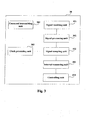
- Fig. 7 is a block diagram of the systematic structure of the terminal equipment 700 of the embodiments of the present invention, in which the above-described signal receiving unit 101, the signal sampling unit 102, the interval measuring unit 103, and the controlling unit 104 are included.
- This figure is exemplary, and other types of structures may also be used to supplement or replace such a structure, so as to realize telecommunications functions or other functions.
- the terminal equipment 700 may further include a central processing unit 100, a communication module 110, an input unit 120, an audio processor 130, a memory 140, a camera 150, a display 160, and a power supply 170.
- the receiving unit 101, the signal sampling unit 102, the interval measuring unit 103, and the controlling unit 104 may be connected directly, may be connected via the central processing unit 100, or may be integrated into the central processing unit 100.
- the central processing unit 100 receives input and controls every components and operations of the terminal equipment 700.
- the input unit 120 provides input to the central processing unit 100.
- the input unit 120 is, for example, a key or a touch input device.
- the camera 150 is used to take image data and provide the taken image data to the central processing unit 100, for use in a conventional manner, such as storage, and transmission, etc.
- the power supply 170 is used to supply electric power to the terminal equipment 700.
- the display 160 is used to display the display objects, such as images, and characters, etc.
- the display may be, for example, an LED display, but it is not limited thereto.
- the memory 140 is coupled to the central processing unit 100.
- the memory 140 may be a solid-state memory, such as a read-only memory (ROM), a random access memory (RAM), and a SIM card, etc. It may be such a memory that stores information when the power is interrupted, may be selectively erased and provided with more data. Examples of such a memory are sometimes referred to as an EPROM, etc.
- the memory 140 may also be certain other types of devices.
- the memory 140 includes a buffer memory 141 (sometimes referred to as a buffer).
- the memory 140 may include an application/function storing portion 142 used to store application programs and function programs, or to execute the operation flow of the terminal equipment 700 via the central processing unit 100.
- the memory 140 may further include a data storing portion 143 used to store data, such as a contact person, digital data, pictures, voices and/or any other data used by other electronic devices.
- a driver storing portion 144 of the memory 140 may include various types of drivers of electronic devices for the communication function and/or for executing other functions (such as application of message transmission, and application of directory, etc.) of the electronic devices.
- the communication module 110 is a transmitter/receiver 110 transmitting and receiving signals via an antenna 111.
- the communication module (transmitter/receiver) 110 is coupled to the central processing unit 100 to provide input signals and receive output signals, this being similar to the case in a conventional mobile phone.
- a plurality of communication modules 110 may be provided in the same electronic device for various communication technologies, such a cellular network module, a Bluetooth module, and/or wireless local network module, etc.
- the communication module (transmitter/receiver) 110 is also coupled to a loudspeaker 131 and a microphone 132 via the audio processor 130, for providing audio output via the loudspeaker 131 and receiving the audio input from the microphone 132, thereby achieving common telecommunications functions.
- the audio processor 130 may include any appropriate buffers, decoders, and amplifiers, etc.
- the audio processor 130 is further coupled to the central processing unit 100, thereby enabling the recording of voices in this device via the microphone 132 and playing the voices stored in this device via the loudspeaker 131.
- each of the parts of the present invention may be implemented by hardware, software, firmware, or a combination thereof.
- multiple steps or methods may be realized by software or firmware that is stored in the memory and executed by an appropriate instruction executing system.
- a discrete logic circuit having a logic gate circuit for realizing logic functions of data signals
- application-specific integrated circuit having an appropriate combined logic gate circuit
- PGA programmable gate array
- FPGA field programmable gate array
- logic and/or steps shown in the flowcharts or described in other manners here may be, for example, understood as a sequencing list of executable instructions for realizing logic functions, which may be implemented in any computer readable medium, for use by an instruction executing system, device or apparatus (such as a system including a computer, a system including a processor, or other systems capable of extracting instructions from an instruction executing system, device or apparatus and executing the instructions), or for use in combination with the instruction executing system, device or apparatus.
Landscapes
- Engineering & Computer Science (AREA)
- General Engineering & Computer Science (AREA)
- Theoretical Computer Science (AREA)
- Signal Processing (AREA)
- Computer Hardware Design (AREA)
- Physics & Mathematics (AREA)
- General Physics & Mathematics (AREA)
- Mobile Radio Communication Systems (AREA)
- Telephone Function (AREA)
Claims (16)
- Appareil de régulation de force d'excitation, comprenant :une unité de réception de signal pour recevoir un signal d'essai pour réguler une force d'excitation transmise par un dispositif périphérique ;caractérisé en ce que l'appareil comprend en outre :une unité d'échantillonnage de signal pour échantillonner le signal d'essai via un signal d'horloge pour obtenir une pluralité de fronts montants et de fronts descendants du signal d'essai ;une unité de mesure d'intervalle pour mesurer l'intervalle de temps entre un front montant et un front descendant, ou entre un front montant et un autre front montant, ou entre un front descendant et un autre front descendant ; etune unité de régulation pour ajuster la force d'excitation imposée au dispositif périphérique selon l'intervalle de temps.
- Appareil de régulation selon la revendication 1, dans lequel l'appareil de régulation comprend en outre :une unité de transmission d'instruction pour transmettre au dispositif périphérique une instruction de test comportant une séquence de données ; etl'unité de réception de signal est en outre utilisée pour recevoir un signal d'essai transmis par le dispositif périphérique selon l'instruction de test.
- Appareil de régulation selon l'une des revendications 1 et 2, dans lequel l'unité de régulation est en outre utilisée pour demander au dispositif périphérique, selon l'intervalle de temps, d'ajuster la force d'excitation.
- Appareil de régulation selon l'une quelconque des revendications 1 à 3, dans lequel l'unité de régulation comprend :une unité de comparaison pour comparer l'intervalle de temps à une valeur prédéterminée, la valeur prédéterminée étant prédéterminée selon la séquence de données dans l'instruction de test ; etune unité d'ajustement pour augmenter la force d'excitation imposée au dispositif périphérique si l'intervalle de temps est inférieur à la valeur prédéterminée, et pour diminuer la force d'excitation imposée au dispositif périphérique si l'intervalle de temps est supérieur à la valeur prédéterminée.
- Appareil de régulation selon l'une quelconque des revendications 1 à 4, dans lequel l'appareil de régulation comprend en outre :une unité de traitement de signal reliée à l'unité de réception de signal pour mettre en mémoire tampon et amplifier le signal d'essai.
- Appareil de régulation selon la revendication 1 ou 2, dans lequel le signal d'horloge est un signal d'horloge de haute fréquence, et l'appareil de régulation comprend en outre :une unité de traitement d'horloge reliée à l'unité d'échantillonnage de signal pour générer le signal d'horloge de haute fréquence par un signal d'horloge de référence, de sorte que l'unité d'échantillonnage de signal effectue un échantillonnage par le signal d'horloge de haute fréquence.
- Appareil de régulation selon la revendication 6, dans lequel l'unité de traitement d'horloge est une boucle à verrouillage de phase, et la fréquence du signal d'horloge de référence est de 26 MHz, et la fréquence du signal d'horloge de haute fréquence est de 1 GHz.
- Appareil de régulation selon l'une quelconque des revendications 1 à 7, dans lequel l'unité de mesure d'intervalle est un oscilloscope à bande large.
- Procédé de régulation de force d'excitation, comprenant le fait :de recevoir un signal d'essai pour réguler une force d'excitation transmise par un dispositif périphérique ;d'échantillonner le signal d'essai reçu via un signal d'horloge pour obtenir une pluralité de fronts montants et de fronts descendants du signal d'essai ;de mesurer l'intervalle de temps entre un front montant et un front descendant, ou entre un front montant et un autre front montant, ou entre un front descendant et un autre front descendant ; etd'ajuster la force d'excitation imposée au dispositif périphérique selon l'intervalle de temps.
- Procédé de régulation selon la revendication 9, dans lequel avant de recevoir le signal d'essai transmis par le dispositif périphérique, le procédé de régulation comprend en outre le fait :de transmettre au dispositif périphérique une instruction de test comportant une séquence de données ; etde recevoir un signal d'essai transmis par le dispositif périphérique selon l'instruction de test.
- Procédé de régulation selon l'une des revendications 9 et 10, dans lequel, après la mesure de l'intervalle de temps, le procédé de régulation comprend en outre le fait :de demander au dispositif périphérique, selon l'intervalle de temps, d'ajuster la force d'excitation.
- Procédé de régulation selon l'une quelconque des revendications 9 à 11, dans lequel l'étape d'ajustement de la force d'excitation imposée au dispositif périphérique selon l'intervalle de temps comprend le fait :de comparer l'intervalle de temps à une valeur prédéterminée, la valeur prédéterminée étant prédéterminée selon la séquence de données dans l'instruction de test ; etd'augmenter la force d'excitation imposée au dispositif périphérique si l'intervalle de temps est inférieur à la valeur prédéterminée, et de diminuer la force d'excitation imposée au dispositif périphérique si l'intervalle de temps est supérieur à la valeur prédéterminée.
- Procédé de régulation selon l'une quelconque des revendications 9 à 12, dans lequel après réception du signal d'essai transmis par le dispositif périphérique, le procédé de régulation comprend en outre le fait :de mettre en mémoire tampon et d'amplifier le signal d'essai.
- Procédé de régulation selon l'une quelconque des revendications 9 à 13, dans lequel le procédé de régulation comprend en outre le fait :de générer un signal d'horloge de haute fréquence par un signal d'horloge de référence ; etd'effectuer un échantillonnage sur le signal d'essai reçu par le signal d'horloge de haute fréquence.
- Procédé de régulation selon la revendication 14, dans lequel la fréquence du signal d'horloge de référence est de 26 MHz, et la fréquence du signal d'horloge de haute fréquence est de 1 GHz.
- Équipement terminal, comprenant l'appareil de régulation tel que revendiqué dans l'une quelconque des revendications 1 à 8.
Applications Claiming Priority (3)
| Application Number | Priority Date | Filing Date | Title |
|---|---|---|---|
| CN201110142269.XA CN102810003B (zh) | 2011-05-30 | 2011-05-30 | 驱动强度的控制装置、方法及终端设备 |
| US13/483,163 US8954013B2 (en) | 2011-05-30 | 2012-05-30 | Driving strength control apparatus, driving strength control method and terminal equipment |
| PCT/IB2012/001050 WO2012164376A1 (fr) | 2011-05-30 | 2012-05-30 | Appareil de régulation de la puissance d'excitation, procédé de régulation de la puissance d'excitation et équipement terminal |
Publications (2)
| Publication Number | Publication Date |
|---|---|
| EP2715552A1 EP2715552A1 (fr) | 2014-04-09 |
| EP2715552B1 true EP2715552B1 (fr) | 2015-06-24 |
Family
ID=47233717
Family Applications (1)
| Application Number | Title | Priority Date | Filing Date |
|---|---|---|---|
| EP12730261.0A Not-in-force EP2715552B1 (fr) | 2011-05-30 | 2012-05-30 | Appareil de régulation de la puissance d'excitation, procédé de régulation de la puissance d'excitation et équipement terminal |
Country Status (4)
| Country | Link |
|---|---|
| US (1) | US8954013B2 (fr) |
| EP (1) | EP2715552B1 (fr) |
| CN (1) | CN102810003B (fr) |
| WO (1) | WO2012164376A1 (fr) |
Cited By (1)
| Publication number | Priority date | Publication date | Assignee | Title |
|---|---|---|---|---|
| CN110736489A (zh) * | 2018-07-18 | 2020-01-31 | 大陆汽车电子(连云港)有限公司 | 传感器性能测试方法及系统 |
Families Citing this family (2)
| Publication number | Priority date | Publication date | Assignee | Title |
|---|---|---|---|---|
| DE102011084143B4 (de) * | 2011-10-07 | 2024-07-04 | Rohde & Schwarz GmbH & Co. Kommanditgesellschaft | Messsoftware unterstütztes Messsystem und Messverfahren |
| KR102557374B1 (ko) * | 2018-09-30 | 2023-07-20 | 광동 오포 모바일 텔레커뮤니케이션즈 코포레이션 리미티드 | 어댑터의 시간 매개 변수의 테스트 방법 및 시스템, 컴퓨터 저장 매체 |
Citations (1)
| Publication number | Priority date | Publication date | Assignee | Title |
|---|---|---|---|---|
| US20050285648A1 (en) * | 2004-06-29 | 2005-12-29 | Intel Corporation | Closed-loop independent DLL-controlled rise/fall time control circuit |
Family Cites Families (6)
| Publication number | Priority date | Publication date | Assignee | Title |
|---|---|---|---|---|
| US6229845B1 (en) * | 1999-02-25 | 2001-05-08 | Qlogic Corporation | Bus driver with data dependent drive strength control logic |
| US6750689B2 (en) * | 2001-03-29 | 2004-06-15 | Intel Corporation | Method and apparatus for correcting a clock duty cycle in a clock distribution network |
| US7437137B2 (en) * | 2003-02-14 | 2008-10-14 | Alan Fiedler | Mixer system |
| TWI221295B (en) * | 2003-11-06 | 2004-09-21 | Via Tech Inc | Circuit for calibrating output driving of dram and method thereof |
| US7230449B2 (en) * | 2005-02-11 | 2007-06-12 | International Business Machines Corporation | Data receiver with a programmable reference voltage to optimize timing jitter |
| US8233336B2 (en) * | 2009-09-25 | 2012-07-31 | Infineon Technologies Ag | Memory controller comprising adjustable transmitter impedance |
-
2011
- 2011-05-30 CN CN201110142269.XA patent/CN102810003B/zh not_active Expired - Fee Related
-
2012
- 2012-05-30 US US13/483,163 patent/US8954013B2/en not_active Expired - Fee Related
- 2012-05-30 EP EP12730261.0A patent/EP2715552B1/fr not_active Not-in-force
- 2012-05-30 WO PCT/IB2012/001050 patent/WO2012164376A1/fr not_active Ceased
Patent Citations (1)
| Publication number | Priority date | Publication date | Assignee | Title |
|---|---|---|---|---|
| US20050285648A1 (en) * | 2004-06-29 | 2005-12-29 | Intel Corporation | Closed-loop independent DLL-controlled rise/fall time control circuit |
Cited By (1)
| Publication number | Priority date | Publication date | Assignee | Title |
|---|---|---|---|---|
| CN110736489A (zh) * | 2018-07-18 | 2020-01-31 | 大陆汽车电子(连云港)有限公司 | 传感器性能测试方法及系统 |
Also Published As
| Publication number | Publication date |
|---|---|
| US8954013B2 (en) | 2015-02-10 |
| US20120306544A1 (en) | 2012-12-06 |
| CN102810003B (zh) | 2015-02-18 |
| EP2715552A1 (fr) | 2014-04-09 |
| CN102810003A (zh) | 2012-12-05 |
| WO2012164376A1 (fr) | 2012-12-06 |
Similar Documents
| Publication | Publication Date | Title |
|---|---|---|
| US9224365B2 (en) | Method and apparatus for reducing interference and mobile terminal | |
| US11121684B2 (en) | Method and apparatus for digital envelope tracking with dynamically changing voltage levels for power amplifier | |
| CN100468978C (zh) | 维持接收机操作的系统和方法 | |
| US20240107388A1 (en) | Timing advance in layer 1/layer 2 intercell mobility | |
| CN115175291B (zh) | 功率控制参数指示方法、终端及网络侧设备 | |
| US11792706B2 (en) | Uplink transmission for dual active protocol stack handover | |
| CN107809263B (zh) | 近场通信装置 | |
| CN108964800B (zh) | 移动终端的天线性能检测方法及系统 | |
| EP2713317A1 (fr) | Carte mémoire flash apte à envoyer des données par l'intermédiaire de réseaux sans fil | |
| EP2715552B1 (fr) | Appareil de régulation de la puissance d'excitation, procédé de régulation de la puissance d'excitation et équipement terminal | |
| US8787512B1 (en) | Synchronization of time accurate strobe (TAS) messages | |
| US11917562B2 (en) | Vehicle-to-everything synchronization method and device | |
| CN108770055A (zh) | 发射功率调整方法、装置及电子装置 | |
| US20160322994A1 (en) | Mobile wireless communications device providing enhanced interference mitigation from wireline transmitter and related methods | |
| CN105518936B (zh) | 基于可变电容的天线调节方法及相关装置 | |
| CN106375031A (zh) | 射频通道的检测方法及移动终端 | |
| US20240406774A1 (en) | Method and apparatus for receiving measurement gap configuration information, method and apparatus for sending measurement gap configuration information, and medium | |
| US20150254858A1 (en) | Auto leveling image capture of a hand-held device | |
| EP4338497B1 (fr) | Compensation de retard de propagation pour synchronisation | |
| US20250097839A1 (en) | Measurement relaxtion method, device apparatus, storage medium and apparatus | |
| US20240179720A1 (en) | Method and apparatus for sending downlink transmission, method and apparatus for receiving downlink transmission, and device and storage medium | |
| US12034663B2 (en) | AP-SRS triggering offset enhancement for further enhanced MIMO | |
| CN115643633B (zh) | 一种定时提前量的调整方法、装置、电子设备及存储介质 | |
| US20260113767A1 (en) | Capability indication method and apparatus, capability determination method and apparatus, and communication apparatus and storage medium | |
| CN112825538B (zh) | 一种应用启动方法、装置、终端设备及存储介质 |
Legal Events
| Date | Code | Title | Description |
|---|---|---|---|
| PUAI | Public reference made under article 153(3) epc to a published international application that has entered the european phase |
Free format text: ORIGINAL CODE: 0009012 |
|
| 17P | Request for examination filed |
Effective date: 20131024 |
|
| AK | Designated contracting states |
Kind code of ref document: A1 Designated state(s): AL AT BE BG CH CY CZ DE DK EE ES FI FR GB GR HR HU IE IS IT LI LT LU LV MC MK MT NL NO PL PT RO RS SE SI SK SM TR |
|
| DAX | Request for extension of the european patent (deleted) | ||
| GRAP | Despatch of communication of intention to grant a patent |
Free format text: ORIGINAL CODE: EPIDOSNIGR1 |
|
| INTG | Intention to grant announced |
Effective date: 20150202 |
|
| GRAS | Grant fee paid |
Free format text: ORIGINAL CODE: EPIDOSNIGR3 |
|
| GRAA | (expected) grant |
Free format text: ORIGINAL CODE: 0009210 |
|
| AK | Designated contracting states |
Kind code of ref document: B1 Designated state(s): AL AT BE BG CH CY CZ DE DK EE ES FI FR GB GR HR HU IE IS IT LI LT LU LV MC MK MT NL NO PL PT RO RS SE SI SK SM TR |
|
| REG | Reference to a national code |
Ref country code: GB Ref legal event code: FG4D |
|
| REG | Reference to a national code |
Ref country code: CH Ref legal event code: EP |
|
| REG | Reference to a national code |
Ref country code: AT Ref legal event code: REF Ref document number: 733193 Country of ref document: AT Kind code of ref document: T Effective date: 20150715 |
|
| REG | Reference to a national code |
Ref country code: IE Ref legal event code: FG4D |
|
| REG | Reference to a national code |
Ref country code: DE Ref legal event code: R096 Ref document number: 602012008248 Country of ref document: DE |
|
| REG | Reference to a national code |
Ref country code: NL Ref legal event code: FP |
|
| PG25 | Lapsed in a contracting state [announced via postgrant information from national office to epo] |
Ref country code: HR Free format text: LAPSE BECAUSE OF FAILURE TO SUBMIT A TRANSLATION OF THE DESCRIPTION OR TO PAY THE FEE WITHIN THE PRESCRIBED TIME-LIMIT Effective date: 20150624 Ref country code: NO Free format text: LAPSE BECAUSE OF FAILURE TO SUBMIT A TRANSLATION OF THE DESCRIPTION OR TO PAY THE FEE WITHIN THE PRESCRIBED TIME-LIMIT Effective date: 20150924 Ref country code: FI Free format text: LAPSE BECAUSE OF FAILURE TO SUBMIT A TRANSLATION OF THE DESCRIPTION OR TO PAY THE FEE WITHIN THE PRESCRIBED TIME-LIMIT Effective date: 20150624 Ref country code: LT Free format text: LAPSE BECAUSE OF FAILURE TO SUBMIT A TRANSLATION OF THE DESCRIPTION OR TO PAY THE FEE WITHIN THE PRESCRIBED TIME-LIMIT Effective date: 20150624 |
|
| REG | Reference to a national code |
Ref country code: AT Ref legal event code: MK05 Ref document number: 733193 Country of ref document: AT Kind code of ref document: T Effective date: 20150624 |
|
| REG | Reference to a national code |
Ref country code: LT Ref legal event code: MG4D |
|
| PG25 | Lapsed in a contracting state [announced via postgrant information from national office to epo] |
Ref country code: LV Free format text: LAPSE BECAUSE OF FAILURE TO SUBMIT A TRANSLATION OF THE DESCRIPTION OR TO PAY THE FEE WITHIN THE PRESCRIBED TIME-LIMIT Effective date: 20150624 Ref country code: BG Free format text: LAPSE BECAUSE OF FAILURE TO SUBMIT A TRANSLATION OF THE DESCRIPTION OR TO PAY THE FEE WITHIN THE PRESCRIBED TIME-LIMIT Effective date: 20150924 Ref country code: GR Free format text: LAPSE BECAUSE OF FAILURE TO SUBMIT A TRANSLATION OF THE DESCRIPTION OR TO PAY THE FEE WITHIN THE PRESCRIBED TIME-LIMIT Effective date: 20150925 Ref country code: RS Free format text: LAPSE BECAUSE OF FAILURE TO SUBMIT A TRANSLATION OF THE DESCRIPTION OR TO PAY THE FEE WITHIN THE PRESCRIBED TIME-LIMIT Effective date: 20150624 |
|
| PG25 | Lapsed in a contracting state [announced via postgrant information from national office to epo] |
Ref country code: EE Free format text: LAPSE BECAUSE OF FAILURE TO SUBMIT A TRANSLATION OF THE DESCRIPTION OR TO PAY THE FEE WITHIN THE PRESCRIBED TIME-LIMIT Effective date: 20150624 |
|
| PG25 | Lapsed in a contracting state [announced via postgrant information from national office to epo] |
Ref country code: AT Free format text: LAPSE BECAUSE OF FAILURE TO SUBMIT A TRANSLATION OF THE DESCRIPTION OR TO PAY THE FEE WITHIN THE PRESCRIBED TIME-LIMIT Effective date: 20150624 Ref country code: PL Free format text: LAPSE BECAUSE OF FAILURE TO SUBMIT A TRANSLATION OF THE DESCRIPTION OR TO PAY THE FEE WITHIN THE PRESCRIBED TIME-LIMIT Effective date: 20150624 Ref country code: CZ Free format text: LAPSE BECAUSE OF FAILURE TO SUBMIT A TRANSLATION OF THE DESCRIPTION OR TO PAY THE FEE WITHIN THE PRESCRIBED TIME-LIMIT Effective date: 20150624 Ref country code: ES Free format text: LAPSE BECAUSE OF FAILURE TO SUBMIT A TRANSLATION OF THE DESCRIPTION OR TO PAY THE FEE WITHIN THE PRESCRIBED TIME-LIMIT Effective date: 20150624 Ref country code: IS Free format text: LAPSE BECAUSE OF FAILURE TO SUBMIT A TRANSLATION OF THE DESCRIPTION OR TO PAY THE FEE WITHIN THE PRESCRIBED TIME-LIMIT Effective date: 20151024 Ref country code: PT Free format text: LAPSE BECAUSE OF FAILURE TO SUBMIT A TRANSLATION OF THE DESCRIPTION OR TO PAY THE FEE WITHIN THE PRESCRIBED TIME-LIMIT Effective date: 20151026 Ref country code: RO Free format text: LAPSE BECAUSE OF NON-PAYMENT OF DUE FEES Effective date: 20150624 Ref country code: SK Free format text: LAPSE BECAUSE OF FAILURE TO SUBMIT A TRANSLATION OF THE DESCRIPTION OR TO PAY THE FEE WITHIN THE PRESCRIBED TIME-LIMIT Effective date: 20150624 |
|
| REG | Reference to a national code |
Ref country code: DE Ref legal event code: R097 Ref document number: 602012008248 Country of ref document: DE |
|
| PG25 | Lapsed in a contracting state [announced via postgrant information from national office to epo] |
Ref country code: IT Free format text: LAPSE BECAUSE OF FAILURE TO SUBMIT A TRANSLATION OF THE DESCRIPTION OR TO PAY THE FEE WITHIN THE PRESCRIBED TIME-LIMIT Effective date: 20150624 Ref country code: DK Free format text: LAPSE BECAUSE OF FAILURE TO SUBMIT A TRANSLATION OF THE DESCRIPTION OR TO PAY THE FEE WITHIN THE PRESCRIBED TIME-LIMIT Effective date: 20150624 |
|
| PLBE | No opposition filed within time limit |
Free format text: ORIGINAL CODE: 0009261 |
|
| STAA | Information on the status of an ep patent application or granted ep patent |
Free format text: STATUS: NO OPPOSITION FILED WITHIN TIME LIMIT |
|
| 26N | No opposition filed |
Effective date: 20160329 |
|
| PGFP | Annual fee paid to national office [announced via postgrant information from national office to epo] |
Ref country code: NL Payment date: 20160510 Year of fee payment: 5 |
|
| PGFP | Annual fee paid to national office [announced via postgrant information from national office to epo] |
Ref country code: DE Payment date: 20160524 Year of fee payment: 5 |
|
| PG25 | Lapsed in a contracting state [announced via postgrant information from national office to epo] |
Ref country code: SI Free format text: LAPSE BECAUSE OF FAILURE TO SUBMIT A TRANSLATION OF THE DESCRIPTION OR TO PAY THE FEE WITHIN THE PRESCRIBED TIME-LIMIT Effective date: 20150624 Ref country code: BE Free format text: LAPSE BECAUSE OF NON-PAYMENT OF DUE FEES Effective date: 20160531 |
|
| PG25 | Lapsed in a contracting state [announced via postgrant information from national office to epo] |
Ref country code: BE Free format text: LAPSE BECAUSE OF FAILURE TO SUBMIT A TRANSLATION OF THE DESCRIPTION OR TO PAY THE FEE WITHIN THE PRESCRIBED TIME-LIMIT Effective date: 20150624 Ref country code: LU Free format text: LAPSE BECAUSE OF FAILURE TO SUBMIT A TRANSLATION OF THE DESCRIPTION OR TO PAY THE FEE WITHIN THE PRESCRIBED TIME-LIMIT Effective date: 20160530 |
|
| REG | Reference to a national code |
Ref country code: CH Ref legal event code: PL |
|
| GBPC | Gb: european patent ceased through non-payment of renewal fee |
Effective date: 20160530 |
|
| PG25 | Lapsed in a contracting state [announced via postgrant information from national office to epo] |
Ref country code: CH Free format text: LAPSE BECAUSE OF NON-PAYMENT OF DUE FEES Effective date: 20160531 Ref country code: LI Free format text: LAPSE BECAUSE OF NON-PAYMENT OF DUE FEES Effective date: 20160531 |
|
| REG | Reference to a national code |
Ref country code: IE Ref legal event code: MM4A |
|
| REG | Reference to a national code |
Ref country code: FR Ref legal event code: ST Effective date: 20170131 |
|
| PG25 | Lapsed in a contracting state [announced via postgrant information from national office to epo] |
Ref country code: FR Free format text: LAPSE BECAUSE OF NON-PAYMENT OF DUE FEES Effective date: 20160531 |
|
| PG25 | Lapsed in a contracting state [announced via postgrant information from national office to epo] |
Ref country code: GB Free format text: LAPSE BECAUSE OF NON-PAYMENT OF DUE FEES Effective date: 20160530 Ref country code: IE Free format text: LAPSE BECAUSE OF NON-PAYMENT OF DUE FEES Effective date: 20160530 |
|
| PG25 | Lapsed in a contracting state [announced via postgrant information from national office to epo] |
Ref country code: SE Free format text: LAPSE BECAUSE OF FAILURE TO SUBMIT A TRANSLATION OF THE DESCRIPTION OR TO PAY THE FEE WITHIN THE PRESCRIBED TIME-LIMIT Effective date: 20150624 |
|
| REG | Reference to a national code |
Ref country code: DE Ref legal event code: R119 Ref document number: 602012008248 Country of ref document: DE |
|
| REG | Reference to a national code |
Ref country code: NL Ref legal event code: MM Effective date: 20170601 |
|
| PG25 | Lapsed in a contracting state [announced via postgrant information from national office to epo] |
Ref country code: NL Free format text: LAPSE BECAUSE OF NON-PAYMENT OF DUE FEES Effective date: 20170601 |
|
| PG25 | Lapsed in a contracting state [announced via postgrant information from national office to epo] |
Ref country code: DE Free format text: LAPSE BECAUSE OF NON-PAYMENT OF DUE FEES Effective date: 20171201 |
|
| PG25 | Lapsed in a contracting state [announced via postgrant information from national office to epo] |
Ref country code: HU Free format text: LAPSE BECAUSE OF FAILURE TO SUBMIT A TRANSLATION OF THE DESCRIPTION OR TO PAY THE FEE WITHIN THE PRESCRIBED TIME-LIMIT; INVALID AB INITIO Effective date: 20120530 Ref country code: SM Free format text: LAPSE BECAUSE OF FAILURE TO SUBMIT A TRANSLATION OF THE DESCRIPTION OR TO PAY THE FEE WITHIN THE PRESCRIBED TIME-LIMIT Effective date: 20150624 Ref country code: CY Free format text: LAPSE BECAUSE OF FAILURE TO SUBMIT A TRANSLATION OF THE DESCRIPTION OR TO PAY THE FEE WITHIN THE PRESCRIBED TIME-LIMIT Effective date: 20150624 |
|
| PG25 | Lapsed in a contracting state [announced via postgrant information from national office to epo] |
Ref country code: TR Free format text: LAPSE BECAUSE OF FAILURE TO SUBMIT A TRANSLATION OF THE DESCRIPTION OR TO PAY THE FEE WITHIN THE PRESCRIBED TIME-LIMIT Effective date: 20150624 Ref country code: MT Free format text: LAPSE BECAUSE OF NON-PAYMENT OF DUE FEES Effective date: 20160531 Ref country code: MC Free format text: LAPSE BECAUSE OF FAILURE TO SUBMIT A TRANSLATION OF THE DESCRIPTION OR TO PAY THE FEE WITHIN THE PRESCRIBED TIME-LIMIT Effective date: 20150624 Ref country code: MK Free format text: LAPSE BECAUSE OF FAILURE TO SUBMIT A TRANSLATION OF THE DESCRIPTION OR TO PAY THE FEE WITHIN THE PRESCRIBED TIME-LIMIT Effective date: 20150624 |
|
| PG25 | Lapsed in a contracting state [announced via postgrant information from national office to epo] |
Ref country code: AL Free format text: LAPSE BECAUSE OF FAILURE TO SUBMIT A TRANSLATION OF THE DESCRIPTION OR TO PAY THE FEE WITHIN THE PRESCRIBED TIME-LIMIT Effective date: 20150624 |