EP2715384B1 - Method for operating a hall sensor assembly, and hall sensor assembly - Google Patents
Method for operating a hall sensor assembly, and hall sensor assembly Download PDFInfo
- Publication number
- EP2715384B1 EP2715384B1 EP12728424.8A EP12728424A EP2715384B1 EP 2715384 B1 EP2715384 B1 EP 2715384B1 EP 12728424 A EP12728424 A EP 12728424A EP 2715384 B1 EP2715384 B1 EP 2715384B1
- Authority
- EP
- European Patent Office
- Prior art keywords
- value
- hall sensor
- signal
- input signal
- values
- Prior art date
- Legal status (The legal status is an assumption and is not a legal conclusion. Google has not performed a legal analysis and makes no representation as to the accuracy of the status listed.)
- Active
Links
Images


Classifications
-
- G—PHYSICS
- G01—MEASURING; TESTING
- G01R—MEASURING ELECTRIC VARIABLES; MEASURING MAGNETIC VARIABLES
- G01R33/00—Arrangements or instruments for measuring magnetic variables
- G01R33/02—Measuring direction or magnitude of magnetic fields or magnetic flux
- G01R33/06—Measuring direction or magnitude of magnetic fields or magnetic flux using galvano-magnetic devices
- G01R33/07—Hall effect devices
- G01R33/072—Constructional adaptation of the sensor to specific applications
-
- G—PHYSICS
- G01—MEASURING; TESTING
- G01R—MEASURING ELECTRIC VARIABLES; MEASURING MAGNETIC VARIABLES
- G01R33/00—Arrangements or instruments for measuring magnetic variables
- G01R33/0023—Electronic aspects, e.g. circuits for stimulation, evaluation, control; Treating the measured signals; calibration
- G01R33/0029—Treating the measured signals, e.g. removing offset or noise
-
- G—PHYSICS
- G01—MEASURING; TESTING
- G01R—MEASURING ELECTRIC VARIABLES; MEASURING MAGNETIC VARIABLES
- G01R33/00—Arrangements or instruments for measuring magnetic variables
- G01R33/0023—Electronic aspects, e.g. circuits for stimulation, evaluation, control; Treating the measured signals; calibration
- G01R33/0035—Calibration of single magnetic sensors, e.g. integrated calibration
-
- G—PHYSICS
- G01—MEASURING; TESTING
- G01R—MEASURING ELECTRIC VARIABLES; MEASURING MAGNETIC VARIABLES
- G01R33/00—Arrangements or instruments for measuring magnetic variables
- G01R33/02—Measuring direction or magnitude of magnetic fields or magnetic flux
- G01R33/06—Measuring direction or magnitude of magnetic fields or magnetic flux using galvano-magnetic devices
- G01R33/07—Hall effect devices
- G01R33/072—Constructional adaptation of the sensor to specific applications
- G01R33/075—Hall devices configured for spinning current measurements
Definitions
- the present invention relates to a method for operating a Hall sensor arrangement and a Hall sensor arrangement.
- Hall sensor arrangements are used to determine a magnetic field.
- Hall sensors usually show an offset voltage, that is a non-zero output voltage between two contacts of the Hall sensor, provided that a current flows between two other contacts of the Hall sensor, even if the Hall sensor is not in a magnetic field.
- the sensor element comprises a measuring element with four contact terminals, a switching device and a control device.
- a tax will be between a first and a second contact terminal in a first measurement phase with a first polarity and in a second measurement phase applied with a polarity opposite to the first polarity.
- the object of the present invention is to provide a method for operating a Hall sensor arrangement and a Hall sensor arrangement with which a residual offset value can be determined during operation.
- a method for operating a Hall sensor arrangement comprises setting at least two values, which are different in magnitude, of an input signal of a Hall sensor of the Hall sensor arrangement. Furthermore, the associated values of an output signal of the Hall sensor are determined. In addition, a residual offset value of the output signal is determined as a function of the values of the output signal which were determined at the at least two values of the input signal.
- the offset component of the output signal and the magnetic field-dependent useful component of the output signal depend in different ways on the height of the input signal of the Hall sensor. Therefore, advantageously by applying the Hall sensor with two different in height values of the input signal, the residual offset value of the output signal can be determined.
- a calibration of the Hall sensor arrangement by means of determining the residual offset value in Operation possible.
- the calibration can also be carried out with an applied external magnetic field of unknown magnetic field strength.
- the output signal is provided only after complete cycling through the phases of a cycle of the current spinning technique.
- the value of the input signal is constant during the phases of the cycle of the current spinning technique.
- the values of the output signal associated with the at least two values of the input signal are each provided by means of a separate cycle of the current spinning technique.
- the at least two values of the output signal are thus determined at the at least two values of the input signal by means of at least two cycles of the current spinning technique.
- the current spinning technique can be referred to as current-rotation technology, current-rotation method or method of rotating operating currents.
- the offset in the values of the output signal is already reduced by the current spinning technique before the residual offset value is determined by the evaluation of the at least two values of the output signal and a magnetic field signal is generated by the Hall sensor arrangement which has no offset influence or an offset influence has significantly reduced offset influence. Consequently, advantageously, the magnetic field signal indicates the magnetic field strength with high accuracy.
- the input signal can be realized as current or voltage.
- the residual offset value is calculated in dependence on the at least two values of the input signal and the values of the output signal determined at the at least two values of the input signal.
- the residual offset value is calculated as a function of the values of the output signal determined at the at least two values of the input signal and a scaling factor between two values of the set of the at least two values of the input signal.
- the scaling factor and a value from the set of at least two values of the input signal may be used in determining the remainder offset value.
- the scaling factor is used in determining the residual offset value.
- the calculation does not include any value of the input signal.
- the at least two values of the input signal are predetermined values.
- the calculation of the residual offset value in the Hall sensor arrangement can advantageously be simplified in such a way that the values of the input signal are combined with other parameters in equations and are no longer explicitly stated.
- the residual offset value may be a residual offset voltage or an offset factor.
- a calibration phase is connected between a first and a second operating phase.
- the residual offset value is determined.
- the value of the magnetic field is determined as a function of the residual offset value.
- the Hall sensor arrangement is operated in a first calibration phase, then in the first operating phase, then again in a second calibration phase and then again in the second operating phase. Since the Hall sensor arrangement can advantageously be calibrated during operation, calibration and operating phases can alternate several times. Thus, the influence of changes in the offset value, which are produced by aging, temperature changes or mechanical stress, for example in soldering processes, can be reduced.
- the calibration phase is triggered when a trigger signal is supplied to the Hall sensor assembly.
- a clock signal is generated which starts a calibration phase at predetermined time intervals.
- the clock signal has a constant frequency.
- the calibration phase is triggered when a temperature change of the Hall sensor arrangement is greater than a predetermined limit value.
- the Hall sensor arrangement has a temperature sensor which provides a temperature signal with which the temperature change is determined.
- the Hall sensor arrangement can be integrated in a system.
- a system may be, for example, a motor vehicle, a machine tool, an ammeter, a compass or a robot.
- the calibration phase is triggered while the system is in an idle state.
- the disturbances are kept low in a resting state of the system, so that a particularly high accuracy in the determination of the residual offset value is achieved.
- the residual offset value is a residual offset voltage.
- VOFF is the value of the residual offset voltage
- k is the value of an offset factor
- I is the value of the input signal
- n is the value of an exponent.
- the residual offset value is an offset factor.
- V is the value of the output signal
- B is the value of the magnetic field
- S is the value of a sensitivity
- I is the value of the input signal
- VOFF is the value of the residual offset voltage.
- the value of the sensitivity is predetermined.
- a coil is arranged in such a way to the Hall sensor, that the magnetic field of the coil influences the magnetic field detected by the Hall sensor, and the value of the sensitivity is determined at the at least two values of the input signal by means of the coil.
- the Hall sensor arrangement is suitable or designed for carrying out the method for operating the Hall sensor arrangement.
- a Hall sensor arrangement comprises a Hall sensor, a signal source and a determination unit.
- the signal source is coupled to an input of the Hall sensor.
- the determination unit is coupled to an output of the Hall sensor.
- the signal source is set up to provide at least two absolute values of an input signal of the Hall sensor.
- the determination unit is set up to determine a residual offset value of an output signal of the Hall sensor as a function of the values of the output signal which are determined at the at least two values of the input signal.
- the residual offset value can be determined by means of two different values of the input signal.
- the Hall sensor comprises a Hall element and an input circuit having an input of the Hall sensor with the Hall element connects. Furthermore, the Hall sensor comprises an output circuit and an evaluation circuit which connect the Hall element to an output of the Hall sensor. The output circuit and the evaluation circuit are connected in series with each other. An output signal provided by the evaluation circuit is provided only after completely passing through the phases of a cycle of the current spinning technique. The input circuit, the output circuit and the evaluation circuit are used to carry out the current spinning technique.
- At least one value of the input signal is at least 1.5 times the smallest value of the input signal. There is thus at least a difference of 50% between two values of the input signal, so that the values of the input signal and thus the values of the output signal differ significantly. This facilitates numerical stable calculation of the residual offset value.
- the Hall sensor arrangement may comprise a semiconductor body.
- the semiconductor body may comprise a silicon substrate.
- the Hall sensor, the signal source and the detection unit are arranged on a first main surface of the semiconductor body.
- the Hall sensor assembly includes a coil.
- the coil may be arranged on the first main surface of the semiconductor body.
- the coil can be a Hall sensor be arranged so that the coil generates a magnetic field which is detected by the Hall sensor.
- the Hall sensor detects the sum of the external magnetic field and the magnetic field generated by the coil.
- FIG. 1A shows an exemplary embodiment of a Hall sensor assembly.
- the Hall sensor arrangement 10 comprises a Hall sensor 11, a signal source 12 and a determination unit 13.
- the signal source 12 is connected at an output to an input of the Hall sensor 11.
- An output of the Hall sensor 11 is coupled to a signal input of the determination unit 13.
- a control output of the determination unit 13 in turn is connected to an input of the signal source 12.
- the Hall sensor 11 comprises a Hall element 14, an input circuit 15 and an output circuit 16.
- the input circuit 15 connects the input of the Hall sensor 11 with the Hall element 14.
- the Hall element 14 is connected via the output circuit 16 to the output of the Hall sensor 11.
- An evaluation circuit 17 is arranged between the output of the output circuit 16 and the output of the Hall sensor 11. Between the output of the output circuit 16 and the evaluation circuit 17, an amplifier 18 is arranged.
- the determination unit 13 has a control circuit 19, a memory 20 and a calculation unit 21.
- the memory 20 is connected to the signal input of the determination unit 13. Furthermore, the memory 20 is coupled to the calculation unit 21 and the control circuit 19. Likewise, the calculation unit 21 is connected to the control circuit 19.
- the control circuit 19 is connected to the control output of the determination unit 13.
- the determination unit 13 has a further memory 22 and a subtracter 23. An input of the subtractor 23 is connected to the signal input of the determination unit 13. Another input of the subtracter 23 is via the further memory 22 is coupled to an output of the calculation unit 21.
- the determination unit 13 comprises a comparator 24, which is connected on the input side to the memory 20 and the control circuit 19.
- the determination unit 13 has a trigger input 25.
- the determination unit 13 is implemented as a digital signal processor. Alternatively, the determination unit 13 is implemented as a microcontroller or microprocessor.
- the signal source 12 outputs an input signal I to the Hall sensor 11.
- the input signal I is realized as a current.
- the signal source 12 is designed as a bias circuit.
- the Hall sensor 11 provides an output signal V at its output.
- the output signal V is in the form of a voltage.
- the input circuit 15, the Hall element 14 and the output circuit 16 convert the input signal I into a sensor signal VS.
- the input circuit 15, the Hall element 14 and the output circuit 16 together form a chopped sensor element.
- the sensor signal VS is converted by the amplifier 18 into an amplified sensor signal AV.
- the evaluation circuit 17 generates from the amplified sensor signal AV, the output signal V of the Hall sensor 11.
- the evaluation circuit 17 is implemented as a de-chop circuit.
- the evaluation circuit 17 may include a switch, an inverter, a comparator or an analog-to-digital converter.
- the output signal V is fed to the signal input of the determination unit 13.
- the output signal V is supplied to the memory 20 and the subtracter 23.
- the subtracter 23 outputs a magnetic field signal SB on the output side.
- the subtractor 23 is implemented as a digital subtractor.
- a trigger signal STR at the trigger input 25 triggers a calibration according to one of the methods described below.
- the input circuit 15 and the output circuit 16 have switches. Thus, according to the current spinning technique, the terminals of the Hall element 14 are periodically switched.
- the sensor signal VS and the amplified sensor signal AV thus depend on the position of the switches in the input and output circuits 15, 16.
- the evaluation circuit 17 is designed to generate the output signal V from the sensor signal VS or the amplified sensor signal AV.
- the output signal V is thus provided after carrying out the current spinning technique.
- the output signal V is generated by the evaluation circuit 17 from the values of the sensor signal VS or the amplified sensor signal AV generated during a period of one cycle of the current spinning technique.
- the output signal V thus has only a small offset signal component, which is also referred to as the residual offset signal component.
- the determination unit 13 is implemented such that it determines a residual offset value in the form of a residual offset voltage VOFF and stores it in the further memory 22.
- the subtracter 23 thus subtracts the residual offset voltage VOFF from the output signal V, so that the magnetic field signal SB has a significantly reduced residual offset component.
- the magnetic field signal SB emitted by the subtracter 23 is thus approximately offset-free.
- the magnetic field signal SB is directly proportional to the magnetic field B.
- VOFF is the value of the residual offset voltage
- k is the value of an offset factor
- I is the value of the input signal
- n is the value of an exponent.
- the offset factor k is a unit-based number.
- the offset factor k has the unit volt / ampere n .
- the Hall sensor 11 has an analog-to-digital converter which is arranged between the evaluation circuit 17 and the output of the Hall sensor 11.
- the output signal V is thus present as a digital signal.
- the output signal V is designed as a current.
- the input signal I is realized as a voltage.
- the output signal V may be a voltage or a current.
- the Hall sensor arrangement 10 comprises further Hall elements.
- the further Hall elements can form a Hall sensor array together with the Hall element 14.
- the different Hall elements can be connected in parallel and / or in series with one another.
- the determination unit 13 may be designed to determine an angle information from the signal of a plurality of Hall sensors.
- the determination unit 13 can be designed to determine the angle information from the signal of a plurality of Hall sensors in accordance with the method of the coordinate rotation digital computer, abbreviated CORDIC method.
- the determination unit 13 can use alternative algorithms, such as the calculation by means of a table, English lookup table, for determining the angle information from the signal of several Hall sensors.
- FIG. 1B shows an exemplary measurement at a Hall sensor 11.
- the output signal V, the residual offset voltage VOFF and the magnetic field signal SB are indicated.
- Figure 1C shows the in FIG. 1B specified values of the residual offset voltage VOFF in an enlarged view.
- the residual offset voltage VOFF is plotted against the input signal I.
- the solid line was calculated from the measured values according to the least squares principle.
- the residual offset value VOFF is proportional to I 3.2238 .
- the non-linear dependence of the residual offset voltage VOFF on the input signal I is used to extract the residual offset voltage VOFF from at least two measurements taken at two different values of the input signal I.
- V ⁇ 2 B ⁇ S I ⁇ 2 ⁇ I ⁇ 2 + VOFF ⁇ 2 .
- VOFF ⁇ 2 k ⁇ I ⁇ 2 n .
- V1 and V2 are a first and a second value of the output signal
- B the value of a magnetic field
- S (I1) and S (I2) the first and the second value of a sensitivity
- I1 and 12 of the first and the second value of the input signal and VOFF1 and VOFF2 are the first and the second value of the residual offset voltage, respectively.
- the absolute value of the first value I1 of the input signal I and the absolute value of the second value 12 of the input signal I are different.
- the absolute value of the first value I1 of the input signal I is smaller than the absolute value of the second value 12 of the input signal I.
- the predetermined value Iv of the input signal I may be equal to the first value I1 or the second value 12 or a value of the input signal I lying between the first value I1 and the second value 12.
- vv B ⁇ S iv ⁇ iv + VOFFv .
- VOFFv k ⁇ iv n .
- the predetermined value Iv of the input signal I may be outside the range limited by the first value I1 and the second value 12.
- the measurement duration can be the period of a cycle of the current spinning technique.
- the ratio of the measurement duration at the first value 12 to the measurement duration at the second value I1 can be greater than the ratio I1 / I2, provided I1> I2.
- the ratio of the measurement duration at the first value 12 to the measurement duration at the second value I1 can be smaller than the ratio I1 / I2, provided I1 ⁇ I2. Thus, the influence of the noise is reduced.
- the current dependence of the sensitivity S is neglected. Furthermore, a given value is used for the exponent n.
- VOFF ⁇ 1 k ⁇ I ⁇ 1 n .
- VOFF ⁇ 2 k ⁇ I ⁇ 2 n .
- VOFFv k ⁇ iv n .
- At least one of the values I1, 12, Iv of the input signal I, the offset voltage VOFF and / or the offset factor k are stored in the further memory 22.
- not only the offset factor k, but also the value of the exponent n are determined.
- the first and second values V1, V2 of the output signal V at the first and second values I1, 12 of the input signal I and additionally a third value V3 of the output signal V at a third value 13 of the input signal I are measured.
- the first, the second and the third value I1, 12, 13 of the input signal I have different amounts.
- the determination of the quantities k, n and VOFF takes place by means of an iterative calculation method.
- VOFF ⁇ 3 k ⁇ I ⁇ 3 n . I ⁇ 1 ⁇ I ⁇ 2 ⁇ I ⁇ 3
- the control circuit 19 sets the signal source 12 by means of the control signal SI such that the first value I1 of the input signal I is provided to the Hall sensor 11. The first value V1 of the output signal V of the Hall sensor 11 is then stored in the determination unit 13 in the memory 20. Furthermore, the control circuit 19 provides the second value 12 of the input signal I by means of the control signal SI, and the second value V2 of the output signal V is stored in the determination unit 13 in the memory 20. Furthermore, the signal source 12 is adjusted by control circuit 19 by means of the control signal SI such that the third value 13 of the input signal I is output to the Hall sensor 11, which in turn provides the third value V3 of the output signal V. The third value V3 of the output signal V is stored in the memory 20.
- the determination unit 13 calculates the value of the exponent n and the value of the offset factor k. Furthermore, the determination unit 13 calculates the value of the residual offset voltage VOFF, for example, at the first, second or third value I1, 12, 13 of the input signal I or a further predetermined value Iv of the input signal I and from this the value of the magnetic field signal SB or the value of the product the value of the magnetic field B and the value of the sensitivity S.
- the first and second embodiments of the method are based on the assumption that the value of the magnetic field B changes only very slightly during the duration of the calibration phase.
- the residual offset voltage VOFF is further reduced by a factor of 0.5 to 0.01 compared to the value of the residual offset voltage VOFF, which has already been reduced by application of the current spinning technique.
- the effort for carrying out the first and the second embodiment the method kept low; For example, no coil is needed.
- the shortest measuring duration is set and for the largest value of the three values I1, 12, 13 of the input signal I the shortest measuring duration.
- a measurement duration between the shortest and the longest measurement duration is set.
- the calibration is performed and then verified.
- the first value I1 of the input signal I is first generated during the calibration phase, the first value V1 of the output signal V is stored, and then the second value 12 of the input signal I is generated.
- the measurement is repeated with the first value I1 of the input signal I and the associated newly determined value V1 'of the output signal V is compared with the first value V1 of the output signal V determined during the calibration phase. The comparison is carried out by the comparator 24 in the determination unit 13. If the two values V1 and V1 'match, it can be assumed that the strength of the magnetic field B has not changed significantly during the calibration phase and the values determined for the offset factor k and the exponent n are used in the subsequent operating phase can.
- further measurements are carried out as control measurements.
- systematic errors due to unfavorable frequency components can be detected.
- At least one value of the input signal I is greater than 1 mA. In an alternative embodiment At least one value of the input signal I is greater than 2 mA.
- FIG. 1D shows an example of measurement results obtained with the first embodiment of the method.
- 19 different Hall sensors were measured.
- the value of the input signal I was 2.25 mA.
- a residual offset voltage VOFF calculated according to the first embodiment of the method a measured residual offset voltage VOFFC and a remaining residual offset voltage VOFFR are indicated.
- the values VOFFC were measured without an external applied field except for the earth magnetic field, whereby the earth magnetic field was not shielded during the measurement.
- the values VOFF of the calculated residual offset voltages were extracted from measurement data determined with an applied external magnetic field of 1.6 mT by the method given above.
- the value VOFFR is the difference between the measured values VOFFC of the residual offset voltage and the calculated values VOFF of the residual offset voltage and corresponds to the strength of the earth's magnetic field in the measuring chamber.
- FIG. 1D thus shows that an offset calibration with an applied external magnetic field, here of 1.6 mT, is possible.
- FIG. 2A shows a further exemplary embodiment of the Hall sensor assembly.
- the Hall sensor assembly 10 according to FIG. 2A is a further education of in Figure 1A shown Hall sensor arrangement.
- the Hall sensor assembly 10 includes a coil 30 which is coupled to the Hall sensor 11.
- the coil 30 is arranged on the Hall element 14.
- the coil 30 is arranged in such a way that the magnetic field generated by the coil 30 contributes to the magnetic field measured by the Hall element 14.
- the Hall sensor assembly 10 includes a power generator 31, whose output is connected to the coil 30. Another control output of the determination unit 13 is connected to the power generator 31.
- the control circuit 19 is connected on the output side to the current generator 31.
- the current generator 31 provides a coil current IC which is supplied to the coil 30.
- the magnetic field generated by the coil 30 is proportional to the value of the coil current IC.
- the determination unit 13 generates a further control signal SIC, which is supplied to the current generator 31 and controls the value of the coil current IC.
- FIG. 2B shows a further exemplary embodiment of the Hall sensor assembly, which is a development of in Figures 1A and 2A shown Hall sensor arrangements is.
- the signal source 12 comprises a current source 32 whose output is connected to the Hall sensor 11.
- the current source 32 is realized controlled.
- the signal source 12 to a digital-to-analog converter 33.
- the current source 32 forms a current output of the digital-to-analog converter 33.
- the current generator 31 is also realized as a current source.
- the power source of the power generator 31 is implemented under control.
- the current source of the current generator 31 represents a further output of the digital-to-analog converter 33.
- the digital-to-analog converter 33 is thus realized as a two-channel digital-to-analog converter.
- the evaluation circuit 17 comprises a low-pass filter. Further, the Hall sensor 11 comprises an analog-to-digital converter 34, which is arranged between the evaluation circuit 17 and the output of the Hall sensor 11. The analog-to-digital converter 34 is connected on the output side to the signal input of the determination unit 13. Furthermore, the Hall sensor arrangement 10 a reference source 35. The reference source 35 is connected to a reference input of the analog-to-digital converter 34.
- the memory 20 and the further memory 22 form in FIG. 2B a shared memory block. The memory 20 and the further memory 22 have memory cells for storing a coil factor CS, various predetermined values I1, 12, 13, Iv of the input signal I and / or different predetermined values of the coil current IC.
- the control circuit 19 has its output connected to the input circuit 15, the output circuit 16, the amplifier 18 and the analog-to-digital converter 34.
- the control circuit 19 thus controls the position of the switches of the input and output circuits 15, 16 for performing the current spinning technique.
- the amplifier 18 is adjusted.
- the amplifier 18 is realized as a chopping amplifier.
- the control circuit 19 controls the analog-to-digital converter 34. It is thereby achieved that a measured value is provided as the output signal V of the determination unit 13 only after a complete cycle has been carried out according to the spinning technique.
- the reference circuit 15 provides a reference signal VREF, which is supplied to the analog-to-digital converter 34.
- the dependence of the sensitivity S (I) on the input signal I is taken into account.
- the dependence of the sensitivity S (I) on the input signal I is determined by means of the coil 30.
- V i + IC is the value of the output signal at a positive coil current and the i-th direction
- V i -IC the value of the output signal at a negative coil current and the ith direction
- IC the value of the coil current and CS the value of the coil factor the coil 30 is.
- the determination of the sensitivity S (I) can be carried out in the presence of an external magnetic field.
- the value of the output signal V is determined to be a value 0 of the coil current IC, at a positive value and at a negative value of the coil current IC.
- the absolute values of the positive and negative values of the coil current IC are identical. Since the determination unit 13 now takes into account the current dependence of the sensitivity S (I), an accurate value of the magnetic field signal SB is determined.
- the sensitivity S (I) and the output signal V at the first and second values I1, 12 of the input signal I are determined by means of the coil 30 during the calibration phase.
- a given value for the exponent n is used.
- the first or the second value I1, 12 of the input signal is used.
- the signal source 12 outputs the first value I1 of the input signal I.
- VOFF ⁇ 2 k ⁇ I ⁇ 2 n .
- the corresponding values V1, V2, V3 of the output signal V are determined in the calibration phase at least for the first, second and third values I1, 12, 13 of the input signal I and also at the first, second and third values I1, 12, 13 of the input signal I, the three values S (I1), S (I2), S (I3) of the sensitivity S (I) are determined by means of the coil 30.
- the value of the exponent n and then the value of the offset factor k determine.
- the already stated iterative calculation method is used.
- a S I ⁇ 3 ⁇ I ⁇ 3 ⁇ V ⁇ 2 ⁇ S I ⁇ 3 ⁇ I ⁇ 3 - V ⁇ 3 ⁇ S I ⁇ 2 ⁇ I ⁇ 2 .
- b S I ⁇ 3 ⁇ I ⁇ 3 ⁇ V ⁇ 3 ⁇ S I ⁇ 1 ⁇ I ⁇ 1 - V ⁇ 1 ⁇ S I ⁇ 3 ⁇ I ⁇ 3 .
- c S I ⁇ 3 ⁇ V ⁇ 1 ⁇ S I ⁇ 2 ⁇ I ⁇ 2 - V ⁇ 2 ⁇ S I ⁇ 1 ⁇ I ⁇ 1 .
- the N values I1, 12, 13, ..., IN the N values V (I1), V (I2), V (I3), ..., V (IN) of the output signal V are determined.
- the first value VOFF1 of the residual offset voltage from the first and the second value V1, V2 of the output signal V the second value VOFF2 the residual offset voltage from the second and the third Value V2, V3 of the output signal V and the N-1te value VOFF_N-1 of the offset voltage from the N-1ten and the Nth value V of the output voltage V determined.
- the first value n1 of the exponent n is calculated.
- the extraction of the first value VOFF1 to the N-1th value VOFF_N-1 of the residual offset voltage VOFF is repeated.
- the iterative calculations continue.
- Figure 2C shows exemplary measurement results that were determined with the third embodiment of the method.
- a value n 3.0 was assumed for the exponent n.
- the value of the input signal I was 2.25 mA.
- FIG. 2D shows an example of measurement results obtained with the fourth embodiment of the method.
- the determined value of the exponent n is different in the various examples of the Hall sensor assemblies 10 and is in a range of 2.88 to 3.17.
- Figures 2C and 2D For each of the 19 examples of the Hall sensor arrangement, the associated values of the residual offset voltage VOFF calculated according to the method described above, the measured residual offset voltage VOFFC, and the remaining residual offset voltage VOFFR are indicated. As already at FIG. 1D 1, the values VOFFC were measured when only the earth's magnetic field influenced the Hall sensor 11.
- the values VOFF of the calculated residual offset voltages were extracted with the third and fourth embodiments of the method from measurement data at an external magnetic field of 1.6 mT.
- the value VOFFR is the difference between the measured values VOFFC and the calculated values VOFF and corresponds to the strength of the earth's magnetic field in the measuring chamber.
- a particularly high accuracy in the determination of the magnetic field B is achieved by means of the third and the fourth embodiment of the method.
- FIG. 3A shows a further exemplary embodiment of the Hall sensor assembly.
- the Hall sensor assembly 10 according to FIG. 3A is a further education in the Figures 1A . 2A and 2B shown embodiments.
- the determination unit 13 has a status signal output 40. At the status signal output 40, the determination unit 13 outputs a status signal STS.
- the status signal STS has a first value during the operating phase and a second value during the calibration phase of the Hall sensor arrangement 10. The status signal STS can thus be used to indicate whether the iterative calibration is complete in the calibration phase.
- the output signal V which can be tapped off at the output of the Hall sensor 11 already corresponds to the magnetic field signal SB.
- the output signal V is fed to the control circuit 19 of the determination unit 13.
- the output signal V is already free from the residual offset value VOFF as soon as the status signal STS indicates that the calibration phase has been successfully completed.
- the subtracter 23 can thus in the embodiment according to FIG. 3A omitted.
- FIG. 3B shows a further exemplary embodiment of the Hall sensor assembly, a further development of the in the Figures 1A . 2A . 2 B and 3A shown embodiments.
- the memory 20 has memory cells for storing the sensitivity S and the coil factor CS.
- the calculation unit 21 determines the value of the exponent n, the offset factor k and the value of the coil current IC.
- the coil current IC thus has no predetermined value.
- the coil current IC has a variable value.
- the coil current IC is provided by means of the digital-to-analog converter 33 and the current generator 31.
- the amplifier 18, the evaluation circuit 17 and the analog-to-digital converter 34 may together be referred to as a channel.
- the evaluation circuit 17 is used for Offsetreduzi für, which is achieved due to the current spinning technique.
- the calculation circuit 21 calculates the value of the exponent n and the value of the offset factor k to determine the value of the coil current IC.
- the output signal V obtained is free from the residual offset voltage VOFF after the calibration phase.
- the calibration phase can also be referred to as the start phase.
- the residual offset voltage VOFF is compensated by means of a magnetic field, which is generated by means of the coil 30.
- the value of the coil current IC depends on the value of the input signal I of the Hall sensor 11 and is determined by means of an iterative method during the calibration phase. While in the first four embodiments of the method the residual offset voltage VOFF is subtracted from the measured value of the output signal V, in the fifth embodiment of the method the magnetic field of the coil 30 compensates for the residual offset voltage VOFF and the output signal V is directly proportional to the magnetic field B.
- the output signal V at the first, second and third values I1, 12, 13 of the input signal I is measured.
- a quasi-permanent recalibration is performed.
- the Hall sensor 11 is calibrated and then determined in the operating phase of the output signal V exclusively at a value, that is about the first, second or third value I1, 12, 13 of the input signal I.
- a recalibration can be triggered according to one of the methods described above.
- the Hall sensor 11 is subjected to three different values I1, 12, 13 of the input signal I.
- the input signal I is realized as current flowing through the Hall element 14.
- a residual offset voltage VOFF is regulated back, in that the coil current IC flows through the coil 30.
- the output signal V increases linearly with the input signal I.
- the value of the exponent n and the value of the offset factor k can be calculated analytically by the determination unit 13.
- the method begins with a value zero of the coil current IC at a first operating point and determines the necessary values of the coil current IC for the second and third operating point such that a linear relationship between the output signal V and the input signal I is achieved.
- the input signal I assumes the first value I1, in the second operating point the input signal I the second value 12 and in the third operating point of the input signal I the third value 13.
- the value of the exponent n and the value of the offset factor k are calculated from the value of the coil current IC and serve as parameters for the calculation of the coil current IC at the first operating point in the next iteration run. Consequently, the value of the exponent n and the value of the offset factor k are determined in an iterative manner.
- VOFF k ⁇ I ⁇ 2 n .
- V ⁇ 2 ⁇ ⁇ 2 ⁇ V ⁇ 1 .
- V ⁇ 3 ⁇ ⁇ 3 ⁇ V ⁇ 1 .
- I ⁇ 2 ⁇ ⁇ 2 ⁇ I ⁇ 1 .
- I ⁇ 3 ⁇ ⁇ 3 ⁇ I ⁇ 1 .
- I ⁇ 2 ⁇ ⁇ 2 ⁇ I ⁇ 1 .
- I ⁇ 3 ⁇ ⁇ 3 ⁇ I ⁇ 1 .
- IC ⁇ 2 ⁇ ⁇ 2 ⁇ I ⁇ 1 .
- CS is the coil factor
- S the sensitivity
- V1 the value of the output signal V at the first value I1 of the input signal I
- V2 the second value of the output signal V at the second value 12 of the input signal I
- V3 the third value of the output signal V at the third value 13 of the input signal I
- IC1 is the first value of the coil current
- IC2 is the second value of the coil current
- IC3 is the third value of the coil current.
- the above loop is run through several times until a convergence criterion is met.
- FIG. 3C shows exemplary results achieved with the fifth embodiment of the method. It is the Output voltage V applied over the input signal I.
- the uppermost curve shows the output signal V without compensation, that is at a value zero of the coil current IC.
- the magnetic field signal SB is given, which corresponds to an ideal signal.
- the value of the magnetic field signal SB depends linearly on the value of the input signal I.
- the output signal V at the sixth iteration step is already very close to the ideal signal.
- the value of the magnetic field was about 50 ⁇ T. The calculations were done with test data.
- Figure 3D shows another exemplary embodiment of the Hall sensor assembly 10, which is a development of the Hall sensor arrangements shown in Figures 1A, 2A, 2B, 3A and 3B.
- the compensation unit 37 comprises a compensation current source 38.
- the compensation current source 38 is connected to the output of the output circuit 16.
- the Hall sensor 11 has a zero point detector 41.
- the zero point detector 41 is arranged between the evaluation circuit 17 and the output of the Hall sensor 11.
- the zero point detector 41 is connected on the output side to the input of the determination unit 13.
- the zero point detector 41 comprises a comparator.
- the evaluation circuit 17 is realized as a low-pass filter.
- the amplifier 18 is designed as an auto-amplifier.
- the output signal V of the Hall sensor 11 thus has the logical values zero and one.
- the magnetic field signal SB is provided by the calculation unit 21.
- a compensation current IK flows through the compensation current source 38.
- the Compensation unit 37 eliminates a part of the offset. The range for the values of the coil current IC can be made small, in that the offset is reduced by means of the compensation unit 37.
- a sixth embodiment of the method is described with the aid of in Figure 3D realized Hall sensor assembly 10 realized.
- the magnetic field B can be determined by the coil current IC flowing through the coil 30.
- the Hall sensor assembly 10 may be used as an electronic compass.
- the sixth embodiment of the method is particularly suitable for the determination of small values of the magnetic field B.
- the value of the exponent n and the value of the offset factor k are extracted as indicated above.
- a first operating point is set.
- the third value 13 of the input signal is output from the signal source 12 and fed to the Hall sensor 11.
- the value of the coil current IC is now adjusted so that the third value V3 of the output signal V reaches zero. From the value of the coil current IC now the proportion is subtracted, which is required to compensate for the offset. The remaining value of the coil current IC is thus proportional to the value of the magnetic field B. From this, the value of the magnetic field B can be calculated.
- the amplifier 18 has a steep translation characteristic. A small change of the sensor signal VS at the input of the amplifier 18 leads to a large change of the amplified sensor signal AV.
- the calculation unit 21 calculates the value of the exponent n and the value of the offset factor k, the value of the offset voltage VOFF or the value of the coil current IC, which corresponds to the offset voltage VOFF. Further, the calculation circuit 21 sets the zero point condition by setting the appropriate value of the coil current IC.
- the value IB is proportional to the value of the magnetic field B.
- the measurement of the magnetic field then depends on the sensitivity S, the coil factor CS and the value of the coil current IC.
- the value of the sensitivity S and the coil factor CS can be determined during a production test.
- the values may be used as predetermined parameters during the entire life of the Hall sensor assembly 11.
- the coil current IC advantageously has a better dynamic range than the channel, since the channel has to cope with the task that the offset voltage of the Hall element 14 is greater than the output signal V due to a small value of the magnetic field B.
- a coil current IC is fed to the coil 30.
- the coil current IC is adjusted so that the zero point condition is reached by the Hall sensor 11. That is, the output signal V is approximately zero.
- the value of the coil current IC depends on the magnetic field B and on the residual offset, which was calculated in a previous iteration step.
- the magnetic field-dependent signal IB can be calculated by subtracting the remaining offset from the value of the coil current IC.
- the channel is reduced to a zero point detector.
- the amplifier 18 in the channel has a high linearity of the gain characteristic.
- the measurement accuracy depends primarily on the digital-to-analog converter 33, so that high accuracy can be achieved with little effort.
- the calibration can be performed with an applied external magnetic field of unknown magnetic field strength.
- the output signal V is provided after performing the current spinning technique.
- the residual offset value is thus already low. Therefore, only low values for the coil current IC are necessary. It is sufficient to design the coil 30 for low currents.
- the Hall sensor 11 comprises in addition to those in Figure 3D components shown an analog-to-digital converter.
- the analog-digital converter is arranged parallel to the zero-point detector 41.
- a reference voltage source can be dispensed with, since the analog-to-digital converter is used exclusively to determine the value of the exponent n and the value of the offset factor k. In this case, a relative accuracy is sufficient.
- the coil 30 is coupled to the Hall sensor 11 via a current path.
- the coil current IC can additionally be used as input signal I for the Hall element 14.
- the coil current IC can flow as an input signal I through the Hall sensor 11.
- the coil current IC flows through both the coil 30 as well as through the Hall element 14. Thus, a power consumption is reduced with advantage.
- the Hall sensor assembly 10 includes a temperature sensor.
- the temperature of the Hall sensor assembly 10 is measured by means of the temperature sensor.
- the temperature coefficient of the sensitivity S is stored in the memory 20. Thus, a temperature compensation can be performed.
- the Hall sensor 11, the Hall element 14 and another Hall element can be connected to each other according to the principle of "offset reduction by pairing together".
- the zero point detector 41 is designed as a window comparator.
- the window comparator indicates as an output signal V whether the signal at the input of the zero point detector 41 is less than a lower threshold, between the lower threshold and an upper threshold, or greater than the upper threshold.
- the lower threshold value has a negative value and the upper threshold value a positive value.
- the upper and lower thresholds are close to 0 volts.
- the compensation unit 37 can be omitted.
- the output of the output circuit 16 is then connected directly to the input of the amplifier 18.
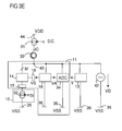
- FIG. 3E shows a further exemplary embodiment of the Hall sensor assembly 10, which is a development of the Hall sensor arrangements shown in Figures 1A, 2A, 2B, 3A, 3B and 3D is.
- the Hall sensor arrangement 10 has a voltage source 42, which is connected to the supply terminals of the Hall sensor 11 and the detection unit 13.
- the voltage source 42 is realized as a constant voltage source.
- the voltage source 42 is connected via the Hall sensor 11 and the signal source 12 to a reference potential terminal 36.
- the signal source 12, the Hall element 14 and the input circuit 15 are arranged between an output of the voltage source 42 and the reference potential terminal 36.
- the Hall element 14 is connected via the output circuit 16, the amplifier 18 and the analog-to-digital converter 34 to the signal input of the detection unit 13.
- the voltage source 42 provides a supply voltage VD on the output side.
- the supply voltage VD is supplied to the Hall sensor 11 and the detection unit 13 to the power supply.
- a reference potential VSS can be tapped.
- At the supply voltage terminal 44 is another supply voltage VDD.
- the coil current IC provided by the current generator 31 flows from the supply voltage terminal 44 via the node 43 to the Hall sensor 11 and thus to the Hall element 14.
- the voltage source 42 serves as a load balance.
- the coil current IC flow partially or completely through the Hall element 14.
- the efficiency of the Hall sensor assembly 10 is increased.
- the Hall sensor 11 comprises a first number M Hall elements. This is by the number M of lines between the node 43 and the Hall element 14 in FIG. 3E indicated.
- FIG. 4A shows an exemplary embodiment of details of a Hall sensor assembly 10, which is a development of the Hall sensor arrangements shown in the above figures.
- the signal source 12 comprises the current source 32 and a further current source 50.
- the current source 32 and the further current source 50 are connected in parallel.
- An output of the current source 32 and an output of the further current source 50 are connected to the output of the signal source 12.
- the Hall element 14 has a first, second, third and fourth connection 51 to 54.
- the Hall element 14 is realized symmetrically.
- the first terminal 51 faces the third terminal 53. Accordingly, the second terminal is opposite to the fourth terminal 55.
- the input circuit 15 comprises a first and a second multiplexer 55, 56.
- the output circuit 16 comprises a third and a fourth multiplexer 57, 58.
- the first, second, third and fourth multiplexers 55 to 58 each have four inputs connected to the first, second, third and fourth terminals 51 to 54 of the Hall element 14 are coupled.
- An output of the first multiplexer 55 is connected to the reference potential terminal 36.
- An output of the second multiplexer 56 is connected to the output of the signal source 12 via the input of the Hall sensor 11.
- An output of the third multiplexer 57 and an output of the fourth multiplexer 58 are coupled to the amplifier 18.
- the amplifier 18 has a first and a second input 59, 60.
- the first input 59 is connected to the output of the third multiplexer 57 and the second input 60 is connected to the output of the fourth multiplexer 58.
- the current source 32 and the further current source 50 are each implemented as constant current sources.
- the current source 32 and the further current source 50 are each separately switched on and off.
- the current source 32 outputs a first current value IP1, which corresponds to the first value I1 of the input signal I.
- the further current source 50 outputs a second current value IP2.
- the sum of the first and the second current value IP1, IP2 corresponds to the second value 12 of the input signal I.
- the current source 32 and the further current source 50 are thus switched on.
- the signal source 12 generates the first and second values I1, 12 of the input signal I according to the first embodiment of the method.
- the detection unit 13 provides four multiplexer control signals S1 to S4 to be supplied to the first, second, third and fourth multiplexers 55 to 58.
- the Current Spinning technique also called Current Spinning method or current rotation method implemented.
- One cycle of the current spinning technique has at least two phases.
- Two opposite terminals of the Hall element 14 are coupled via the first and the second multiplexer 55, 56 to the reference potential terminal 36 and to the output of the signal source 12, respectively. Accordingly, the two further terminals of the Hall element 14 via the third and the fourth multiplexer 57, 58 are coupled to the first and the second input 59, 60 of the amplifier 18.
- the Hall element 14 is sensitive to a magnetic field perpendicular to the surface.
- the output signal V of the Hall sensor 11 is only after complete passage through the phases of a cycle of the current Spinning technique provided. During the phases of a cycle of the current spinning technique, the value of the input signal I is constant. To determine the output signal V at the first value I1 of the input signal I, all phases of the cycle are run according to the current spinning technique. Accordingly, in order to determine the output signal V at the second and / or the third value 12, 13 of the input signal I, the phases of a cycle of the current spinning technique are likewise completely traversed.
- a cycle may have four phases.
- the current spinning technique it is achieved that the current flow in the Hall element 14 assumes four different directions.
- the amount of the sensor signal VS is equal without any offset in all four phases of the current spinning technique.
- each of the four terminals 51 to 54 of the Hall element 14 is thus connected in phase with the output of the signal source 12, the reference potential terminal 36, the first input 59 and the second input 60 of the amplifier 18.
- the sensor signal VS is implemented as a differential signal.
- the sensor signal VS can be tapped between two terminals of the Hall element 14.
- the sensor signal VS is supplied to the first and the second input 59, 60 of the amplifier 18.
- the amplifier 18 converts the sensor signal VS into an amplified sensor signal AV.
- the amplified sensor signal AV is related to the reference potential VSS at the reference potential terminal 36.
- one of the six above-described embodiments of the method according to the proposed principle is performed in addition to the current spinning technique.
- the combination of the current spinning technique and one of the explained six embodiments of the method causes a high accuracy of the magnetic field determination.
- the second current value IP2 corresponds to the second value 12 of the input signal.
- the current source 32 and the further current source 50 are thus switched on individually.
- the current source 32 and the further current source 50 are switched on simultaneously.
- the sum of the first and the second current value IP1, IP2 corresponds to the third value 13 of the input signal I.
- the three different values I1, 12, 13 of the input signal I can be efficiently generated with two current sources 32, 50.
- the signal source 12 comprises an additional current source whose output is connected to the output of the signal source 12.
- one cycle of the current spinning technique comprises exactly two phases. In this case, in a first phase, the first terminal 51 of the Hall element 14 is coupled to the reference potential terminal 36 and the third terminal 53 of the Hall element 14 to the output of the signal source 12 via the first and the second multiplexer 55, 56. In the second phase, the first terminal 51 is coupled to the output of the signal source 12 and the third terminal 53 is coupled to the reference potential terminal 36.
- the second and the fourth connection 52, 54 of the Hall element 14 are alternately coupled to the first and the second input 59, 60 of the amplifier 36 via the third and the fourth multiplexer 57, 58 in the first and the second phase. In the two phases of the cycle thus becomes the direction of the current flowing through the Hall element 14 is rotated by 180 degrees.
- the Hall element 14 comprises further terminals, which are coupled to the signal source 12 and the amplifier 18 by means of the four multiplexers 55 to 58.
- a cycle for operating such a Hall element 14 may have more than four phases.
- FIG. 4B shows another exemplary embodiment of a detail of the Hall sensor 11.
- the Hall sensor 11 includes the Hall element 14 and another Hall element 61.
- the Hall element 14 and the further Hall element 61 are connected according to the principle of geometric spinning.
- the Hall element 14 and the further Hall element 61 are fixedly connected as Hall element pair and can be used instead of the Hall element 14 in one of the above-described Hall sensor arrangements.
- the Hall element 14 and the further Hall element 61 are both coupled to the output of the signal source 12 and the amplifier 18.
- the direction of the current flow through the Hall element 14 has an angle to the direction of the current flow through the further Hall element 61. Preferably, the angle is 45 ° or 90 °.
- the outputs of the Hall element 14 and the further Hall element 61 are connected in parallel.
- the Hall element pair comprising the Hall element 14 and the further Hall element 61, has four terminals 62 to 65.
- a first terminal 62 is connected to the output of the signal source 12, a second terminal 63 to the reference potential terminal 36, a third terminal 64 to the first input 59 of the amplifier 18 and a fourth terminal 65 to the second input 60 of the amplifier 18 is connected.
- the Hall element 14 and the further Hall element 61 have a parallel circuit with respect to the input signals I and the sensor signals VS.
- the first and third terminals 51, 53 of the Hall element 14 are permanently connected to a first and a third terminal 51 ', 53' of the further Hall element 61.
- the second and the fourth connection 52, 54 of the Hall element 14 are permanently connected to a second or a fourth connection 52 ', 54' of the further Hall element 61. Consequently, the input signal terminals 51, 53, 51 ', 53' of the two Hall elements 14, 61 are connected in parallel. Further, the output signal terminals 52, 54, 52 ', 54' of the two Hall elements 14, 61 are connected in parallel.
- the input signal I can be designed as current or voltage.
- the input circuit 15 and the output circuit 16 couples the Hall element pair with the signal source 12 and the amplifier 18.
- the four terminals 62 to 65 of the Hall element pair via the first, second, third and fourth multiplexer 57 to 58 the output of the signal source 12, the reference potential terminal 36 and the first and the second input 59, 60 of the amplifier 18 according to the two or four phases of the current spinning technique connected.
- At least one additional Hall element may be connected to the Hall element 14 and the further Hall element 61 according to the principle of geometric spinning.
- the Hall sensor 11 four Hall elements 14, 61, which together are connected.
Landscapes
- Physics & Mathematics (AREA)
- Condensed Matter Physics & Semiconductors (AREA)
- General Physics & Mathematics (AREA)
- Measuring Magnetic Variables (AREA)
- Hall/Mr Elements (AREA)
- Transmission And Conversion Of Sensor Element Output (AREA)
Description
Die vorliegende Erfindung betrifft ein Verfahren zum Betreiben einer Hallsensoranordnung und eine Hallsensoranordnung.The present invention relates to a method for operating a Hall sensor arrangement and a Hall sensor arrangement.
Hallsensoranordnungen dienen zum Bestimmen eines Magnetfeldes. Hallsensoren zeigen üblicherweise eine Offsetspannung, das heißt eine von Null verschiedene Ausgangsspannung zwischen zwei Kontakten des Hallsensors, sofern ein Strom zwischen zwei weiteren Kontakten des Hallsensors fließt, auch wenn sich der Hallsensor in keinem Magnetfeld befindet.Hall sensor arrangements are used to determine a magnetic field. Hall sensors usually show an offset voltage, that is a non-zero output voltage between two contacts of the Hall sensor, provided that a current flows between two other contacts of the Hall sensor, even if the Hall sensor is not in a magnetic field.
Dokument
Im Dokument "
Dokument
Dokument
Aufgabe der vorliegenden Erfindung ist es, ein Verfahren zum Betreiben einer Hallsensoranordnung und eine Hallsensoranordnung bereitzustellen, mit der ein Rest-Offsetwert im Betrieb ermittelt werden kann.The object of the present invention is to provide a method for operating a Hall sensor arrangement and a Hall sensor arrangement with which a residual offset value can be determined during operation.
Die Aufgabe wird mit dem Verfahren gemäß Patentanspruch 1 und dem Gegenstand des Patentanspruchs 14 gelöst. Weiterbildungen und Ausgestaltungen sind jeweils Gegenstand der abhängigen Ansprüche.The object is achieved by the method according to claim 1 and the subject of
In einer Ausführungsform umfasst ein Verfahren zum Betreiben einer Hallsensoranordnung das Einstellen mindestens zweier betragsmäßig unterschiedlicher Werte eines Eingangssignals eines Hallsensors der Hallsensoranordnung. Weiter werden die dazugehörenden Werte eines Ausgangssignals des Hallsensors bestimmt. Darüber hinaus wird ein Rest-Offsetwert des Ausgangssignals in Abhängigkeit von den Werten des Ausgangsignals ermittelt, die bei den mindestens zwei Werten des Eingangssignals bestimmt wurden.In one embodiment, a method for operating a Hall sensor arrangement comprises setting at least two values, which are different in magnitude, of an input signal of a Hall sensor of the Hall sensor arrangement. Furthermore, the associated values of an output signal of the Hall sensor are determined. In addition, a residual offset value of the output signal is determined as a function of the values of the output signal which were determined at the at least two values of the input signal.
Der Offsetanteil des Ausgangssignals und der magnetfeldabhängige Nutzanteil des Ausgangssignals hängen in unterschiedlicher Weise von der Höhe des Eingangssignals des Hallsensors ab. Daher kann vorteilhafterweise durch Beaufschlagen des Hallsensors mit zwei in der Höhe unterschiedlichen Werten des Eingangssignals der Rest-Offsetwert des Ausgangssignals bestimmt werden. Mit Vorteil ist eine Kalibrierung der Hallsensoranordnung mittels Bestimmen des Rest-Offsetwerts im Betrieb möglich. Vorteilhafterweise kann die Kalibrierung auch bei einem angelegten externen magnetischen Feld mit unbekannter Magnetfeldstärke durchgeführt werden.The offset component of the output signal and the magnetic field-dependent useful component of the output signal depend in different ways on the height of the input signal of the Hall sensor. Therefore, advantageously by applying the Hall sensor with two different in height values of the input signal, the residual offset value of the output signal can be determined. Advantageously, a calibration of the Hall sensor arrangement by means of determining the residual offset value in Operation possible. Advantageously, the calibration can also be carried out with an applied external magnetic field of unknown magnetic field strength.
In einer Ausführungsform wird das Ausgangssignal erst nach vollständigem Durchlaufen der Phasen eines Zyklusses der Current Spinning-Technik bereitgestellt. Dabei ist der Wert des Eingangssignals während der Phasen des Zyklusses der Current Spinning-Technik konstant. Die zu den mindestens zwei Werten des Eingangssignals dazugehörenden Werte des Ausgangssignals werden jeweils mittels eines eigenen Zykluses der Current Spinning-Technik bereitgestellt. Die mindestens zwei Werte des Ausgangssignals werden somit bei den mindestens zwei Werten des Eingangssignals mittels mindestens zwei Zyklen der Current Spinning-Technik bestimmt. Die Current Spinning Technik kann als Strom-Dreh-Technik, Strom-Dreh-Verfahren oder Verfahren der rotierenden Betriebsströme bezeichnet werden. Mit Vorteil wird durch die Current Spinning-Technik der Offset in den Werten des Ausgangssignals bereits reduziert, ehe durch die Auswertung der mindestens zwei Werte des Ausgangssignals der Rest-Offsetwert ermittelt und von der Hallsensoranordnung ein Magnetfeldsignal generiert wird, das keinen Offset-Einfluss oder einen deutlich reduzierten Offset-Einfluss aufweist. Folglich gibt vorteilhafterweise das Magnetfeldsignal die Magnetfeldstärke mit hoher Genauigkeit an.In one embodiment, the output signal is provided only after complete cycling through the phases of a cycle of the current spinning technique. The value of the input signal is constant during the phases of the cycle of the current spinning technique. The values of the output signal associated with the at least two values of the input signal are each provided by means of a separate cycle of the current spinning technique. The at least two values of the output signal are thus determined at the at least two values of the input signal by means of at least two cycles of the current spinning technique. The current spinning technique can be referred to as current-rotation technology, current-rotation method or method of rotating operating currents. Advantageously, the offset in the values of the output signal is already reduced by the current spinning technique before the residual offset value is determined by the evaluation of the at least two values of the output signal and a magnetic field signal is generated by the Hall sensor arrangement which has no offset influence or an offset influence has significantly reduced offset influence. Consequently, advantageously, the magnetic field signal indicates the magnetic field strength with high accuracy.
Das Eingangssignal kann als Strom oder Spannung realisiert sein.The input signal can be realized as current or voltage.
In einer Ausführungsform wird der Rest-Offsetwert in Abhängigkeit von den mindestens zwei Werten des Eingangssignals und den Werten des Ausgangssignals, die bei den mindestens zwei Werten des Eingangssignals bestimmt wurden, berechnet.In one embodiment, the residual offset value is calculated in dependence on the at least two values of the input signal and the values of the output signal determined at the at least two values of the input signal.
Somit gehen nicht nur die Werte des Ausgangssignals, sondern auch die Werte des Eingangssignals in die Berechnung ein.Thus, not only the values of the output signal but also the values of the input signal are included in the calculation.
In einer alternativen Ausführungsform wird der Rest-Offsetwert in Abhängigkeit von den Werten des Ausgangssignals, die bei den mindestens zwei Werten des Eingangssignals bestimmt wurden, und von einem Skalierungsfaktor zwischen zwei Werten aus der Menge der mindestens zwei Werte des Eingangssignals berechnet. Es kann beispielsweise der Skalierungsfaktor und ein Wert aus der Menge der mindestens zwei Werte des Eingangssignals bei der Ermittlung des Rest-Offsetwerts verwendet werden.In an alternative embodiment, the residual offset value is calculated as a function of the values of the output signal determined at the at least two values of the input signal and a scaling factor between two values of the set of the at least two values of the input signal. For example, the scaling factor and a value from the set of at least two values of the input signal may be used in determining the remainder offset value.
Alternativ wird bei der Ermittlung des Rest-Offsetwerts der Skalierungsfaktor verwendet. In die Berechnung geht kein Wert des Eingangssignals ein.Alternatively, the scaling factor is used in determining the residual offset value. The calculation does not include any value of the input signal.
In einer Ausführungsform sind die mindestens zwei Werte des Eingangssignals vorgegebene Werte. Auf Basis der vorgegebenen Werte des Eingangssignals kann mit Vorteil die Berechnung des Rest-Offsetwerts in der Hallsensoranordnung derart vereinfacht sein, dass die Werte des Eingangssignals mit anderen Parametern in Gleichungen zusammengefasst sind und nicht mehr explizit angegeben werden.In one embodiment, the at least two values of the input signal are predetermined values. On the basis of the predetermined values of the input signal, the calculation of the residual offset value in the Hall sensor arrangement can advantageously be simplified in such a way that the values of the input signal are combined with other parameters in equations and are no longer explicitly stated.
Der Rest-Offsetwert kann eine Rest-Offsetspannung oder ein Offsetfaktor sein.The residual offset value may be a residual offset voltage or an offset factor.
In einer Ausführungsform ist eine Kalibrierphase zwischen einer ersten und einer zweiten Betriebsphase geschaltet. In der Kalibrierphase wird der Rest-Offsetwert ermittelt. Hingegen wird in der ersten und in der zweiten Betriebsphase der Wert des Magnetfelds in Abhängigkeit vom Rest-Offsetwert bestimmt.In one embodiment, a calibration phase is connected between a first and a second operating phase. In the calibration phase, the residual offset value is determined. On the other hand, in the first and in the second phase of operation, the value of the magnetic field is determined as a function of the residual offset value.
In einer Ausführungsform wird die Hallsensoranordnung in einer ersten Kalibrierphase, anschließend in der ersten Betriebsphase, wiederum anschließend in einer zweiten Kalibrierphase und wiederum anschließend in der zweiten Betriebsphase betrieben. Da mit Vorteil die Hallsensoranordnung im Betrieb kalibrierbar ist, können sich Kalibrier- und Betriebsphasen mehrfach abwechseln. Somit kann der Einfluss von Änderungen des Offsetwerts, die durch Alterung, Temperaturänderungen oder mechanischen Stress etwa bei Lötprozessen erzeugt werden, verringert werden.In one embodiment, the Hall sensor arrangement is operated in a first calibration phase, then in the first operating phase, then again in a second calibration phase and then again in the second operating phase. Since the Hall sensor arrangement can advantageously be calibrated during operation, calibration and operating phases can alternate several times. Thus, the influence of changes in the offset value, which are produced by aging, temperature changes or mechanical stress, for example in soldering processes, can be reduced.
In einer Ausführungsform wird die Kalibrierphase dann getriggert, wenn ein Triggersignal der Hallsensoranordnung zugeleitet wird.In one embodiment, the calibration phase is triggered when a trigger signal is supplied to the Hall sensor assembly.
In einer alternativen Ausführungsform wird ein Taktsignal generiert, das eine Kalibrierphase in vorgegebenen Zeitabständen startet. Das Taktsignal hat insbesondere eine konstante Frequenz.In an alternative embodiment, a clock signal is generated which starts a calibration phase at predetermined time intervals. In particular, the clock signal has a constant frequency.
In einer alternativen Ausführungsform wird die Kalibrierphase dann getriggert, wenn eine Temperaturänderung der Hallsensoranordnung größer als ein vorgegebener Grenzwert ist. Dazu weist die Hallsensoranordnung einen Temperatursensor auf, welcher ein Temperatursignal bereitstellt, mit dem die Temperaturänderung bestimmt wird.In an alternative embodiment, the calibration phase is triggered when a temperature change of the Hall sensor arrangement is greater than a predetermined limit value. For this purpose, the Hall sensor arrangement has a temperature sensor which provides a temperature signal with which the temperature change is determined.
Die Hallsensoranordnung kann in einem System integriert sein. Ein derartiges System kann etwa ein Kraftfahrzeug, eine Werkzeugmaschine, ein Strommessgerät, ein Kompass oder ein Roboter sein.The Hall sensor arrangement can be integrated in a system. Such a system may be, for example, a motor vehicle, a machine tool, an ammeter, a compass or a robot.
In einer Ausführungsform wird die Kalibrierphase getriggert, während sich das System in einem Ruhezustand befindet. Mit Vorteil sind in einem Ruhezustand des Systems die Störungen gering gehalten, so dass eine besonders hohe Genauigkeit bei der Bestimmung des Rest-Offsetwerts erzielt wird.In one embodiment, the calibration phase is triggered while the system is in an idle state. Advantageously, the disturbances are kept low in a resting state of the system, so that a particularly high accuracy in the determination of the residual offset value is achieved.
In einer Ausführungsform ist der Rest-Offsetwert eine Rest-Offsetspannung. Die Rest-Offsetspannung kann gemäß folgender Gleichung berechnet werden: ![]()
wobei VOFF der Wert der Rest-Offsetspannung, k der Wert eines Offsetfaktors, I der Wert des Eingangssignals und n der Wert eines Exponenten ist.In one embodiment, the residual offset value is a residual offset voltage. The residual offset voltage can be calculated according to the following equation: ![]()
where VOFF is the value of the residual offset voltage, k is the value of an offset factor, I is the value of the input signal, and n is the value of an exponent.
In einer Ausführungsform ist der Rest-Offsetwert ein Offsetfaktor. Der Offsetfaktor kann gemäß folgender Gleichung berechnet werden: ![]()
wobei VOFF der Wert der Rest-Offsetspannung, k der Wert des Offsetfaktors, I der Wert des Eingangssignals und n der Wert des Exponenten ist.In one embodiment, the residual offset value is an offset factor. The offset factor can be calculated according to the following equation: ![]()
where VOFF is the value of the residual offset voltage, k is the value of the offset factor, I is the value of the input signal, and n is the value of the exponent.
In einer Ausführungsform wird der Wert des Magnetfelds gemäß folgender Gleichung ermittelt: ![]()
![]()
In einer Ausführungsform ist der Wert der Empfindlichkeit vorgegeben.In one embodiment, the value of the sensitivity is predetermined.
In einer alternativen Ausführungsform ist eine Spule derart zum Hallsensor angeordnet, dass das Magnetfeld der Spule das vom Hallsensor detektierte Magnetfeld beeinflusst, und wird der Wert der Empfindlichkeit bei den mindestens zwei Werten des Eingangssignals mittels der Spule ermittelt.In an alternative embodiment, a coil is arranged in such a way to the Hall sensor, that the magnetic field of the coil influences the magnetic field detected by the Hall sensor, and the value of the sensitivity is determined at the at least two values of the input signal by means of the coil.
In einer Ausführungsform ist die Hallsensoranordnung zur Durchführung des Verfahrens zum Betreiben der Hallsensoranordnung geeignet oder ausgelegt.In one embodiment, the Hall sensor arrangement is suitable or designed for carrying out the method for operating the Hall sensor arrangement.
In einer Ausführungsform umfasst eine Hallsensoranordnung einen Hallsensor, eine Signalquelle und eine Ermittlungseinheit. Die Signalquelle ist mit einem Eingang des Hallsensors gekoppelt. Die Ermittlungseinheit ist mit einem Ausgang des Hallsensors gekoppelt. Die Signalquelle ist eingerichtet, mindestens zwei betragsmäßig unterschiedliche Werte eines Eingangssignals des Hallsensors bereitzustellen. Weiter ist die Ermittlungseinheit eingerichtet, einen Rest-Offsetwert eines Ausgangssignals des Hallsensors in Abhängigkeit von den Werten des Ausgangssignals, die bei den mindestens zwei Werten des Eingangssignals bestimmt werden, zu ermitteln.
Mit Vorteil ist mittels zweier unterschiedlicher Werte des Eingangssignals der Rest-Offsetwert bestimmbar.In one embodiment, a Hall sensor arrangement comprises a Hall sensor, a signal source and a determination unit. The signal source is coupled to an input of the Hall sensor. The determination unit is coupled to an output of the Hall sensor. The signal source is set up to provide at least two absolute values of an input signal of the Hall sensor. Furthermore, the determination unit is set up to determine a residual offset value of an output signal of the Hall sensor as a function of the values of the output signal which are determined at the at least two values of the input signal.
Advantageously, the residual offset value can be determined by means of two different values of the input signal.
In einer Ausführungsform umfasst der Hallsensor ein Hallelement und eine Eingangsschaltung, die einen Eingang des Hallsensors mit dem Hallelement verbindet. Weiter umfasst der Hallsensor eine Ausgangsschaltung und eine Auswerteschaltung, die das Hallelement mit einem Ausgang des Hallsensors verbinden. Die Ausgangsschaltung und die Auswerteschaltung sind seriell zueinander geschaltet. Ein von der Auswerteschaltung bereitgestelltes Ausgangssignal wird erst nach vollständigem Durchlaufen der Phasen eines Zyklusses der Current Spinning-Technik bereitgestellt. Die Eingangsschaltung, die Ausgangsschaltung und die Auswerteschaltung dienen der Durchführung der Current Spinning-Technik.In an embodiment, the Hall sensor comprises a Hall element and an input circuit having an input of the Hall sensor with the Hall element connects. Furthermore, the Hall sensor comprises an output circuit and an evaluation circuit which connect the Hall element to an output of the Hall sensor. The output circuit and the evaluation circuit are connected in series with each other. An output signal provided by the evaluation circuit is provided only after completely passing through the phases of a cycle of the current spinning technique. The input circuit, the output circuit and the evaluation circuit are used to carry out the current spinning technique.
In einer Weiterbildung beträgt mindestens ein Wert des Eingangssignals mindestens das 1,5-fache des kleinsten Werts des Eingangssignals. Zwischen zwei Werten des Eingangssignals ist somit mindestens ein Unterschied von 50 %, so dass sich die Werte des Eingangssignals und damit die Werte des Ausgangssignals deutlich unterscheiden. Dies erleichtert eine numerische stabile Berechnung des Rest-Offsetwerts.In a further development, at least one value of the input signal is at least 1.5 times the smallest value of the input signal. There is thus at least a difference of 50% between two values of the input signal, so that the values of the input signal and thus the values of the output signal differ significantly. This facilitates numerical stable calculation of the residual offset value.
Die Hallsensoranordnung kann einen Halbleiterkörper umfassen. Der Halbleiterkörper kann ein Siliziumsubstrat aufweisen. Bevorzugt sind der Hallsensor, die Signalquelle und die Ermittlungseinheit auf einer ersten Hauptfläche des Halbleiterkörpers angeordnet.The Hall sensor arrangement may comprise a semiconductor body. The semiconductor body may comprise a silicon substrate. Preferably, the Hall sensor, the signal source and the detection unit are arranged on a first main surface of the semiconductor body.
In einer Ausführungsform umfasst die Hallsensoranordnung eine Spule. Die Spule kann auf der ersten Hauptfläche des Halbleiterkörpers angeordnet sein. Die Spule kann derart zum Hallsensor angeordnet sein, dass die Spule ein Magnetfeld erzeugt, das vom Hallsensor detektiert wird. Dabei detektiert der Hallsensor die Summe aus dem externen Magnetfeld und dem von der Spule erzeugten Magnetfeld.In one embodiment, the Hall sensor assembly includes a coil. The coil may be arranged on the first main surface of the semiconductor body. The coil can be a Hall sensor be arranged so that the coil generates a magnetic field which is detected by the Hall sensor. The Hall sensor detects the sum of the external magnetic field and the magnetic field generated by the coil.
Die Erfindung wird im Folgenden an mehreren Ausführungsbeispielen anhand der Figuren näher erläutert. Funktions- beziehungsweise wirkungsgleiche Komponenten oder Funktionseinheiten tragen gleiche Bezugszeichen. Insoweit sich Komponenten oder Funktionseinheiten in ihrer Funktion entsprechen, wird deren Beschreibung nicht in jeder der folgenden Figuren wiederholt. Es zeigen:
- Figuren 1A bis 1D
- eine beispielhafte Ausführungsform einer Hallsensoranordnung, die zur Durchführung einer ersten und einer zweiten Ausführungsform des Verfahrens zum Betreiben einer Hallsensoranordnung geeignet ist, und beispielhafte Messergebnisse,
- Figuren 2A bis 2D
- weitere beispielhafte Ausführungsformen der Hallsensoranordnung, die zur Durchführung einer dritten und einer vierten Ausführungsform des Verfahrens zum Betreiben der Hallsensoranordnung eingerichtet sind, und dazugehörende Messergebnisse,
- Figuren 3A bis 3E
- weitere beispielhafte Ausführungsformen der Hallsensoranordnung, die zur Durchführung eines fünften und eines sechsten Verfahrens zum Betreiben der Hallsensoranordnung eingerichtet sind, und dazugehörige Messergebnisse sowie
- Figuren 4A und 4B
- beispielhafte Ausführungsformen von Details der Hallsensoranordnung.
- Figures 1A to 1D
- 1 an exemplary embodiment of a Hall sensor arrangement that is suitable for carrying out a first and a second embodiment of the method for operating a Hall sensor arrangement, and exemplary measurement results,
- FIGS. 2A to 2D
- Further exemplary embodiments of the Hall sensor arrangement, which are set up for carrying out a third and a fourth embodiment of the method for operating the Hall sensor arrangement, and associated measurement results,
- FIGS. 3A to 3E
- Further exemplary embodiments of the Hall sensor assembly, which are adapted to carry out a fifth and a sixth method for operating the Hall sensor assembly, and associated measurement results and
- FIGS. 4A and 4B
- exemplary embodiments of details of the Hall sensor assembly.
Die Ermittlungseinheit 13 weist eine Steuerschaltung 19, einen Speicher 20 und eine Berechnungseinheit 21 auf. Der Speicher 20 ist mit dem Signaleingang der Ermittlungseinheit 13 verbunden. Weiter ist der Speicher 20 mit der Berechnungseinheit 21 sowie der Steuerschaltung 19 gekoppelt. Ebenso ist die Berechnungseinheit 21 mit der Steuerschaltung 19 verbunden. Die Steuerschaltung 19 ist mit dem Steuerausgang der Ermittlungseinheit 13 verbunden. Zusätzlich weist die Ermittlungseinheit 13 einen weiteren Speicher 22 und einen Subtrahierer 23 auf. Ein Eingang des Subtrahierers 23 ist mit dem Signaleingang der Ermittlungseinheit 13 verbunden. Ein weiterer Eingang des Subtrahierers 23 ist über den weiteren Speicher 22 mit einem Ausgang der Berechnungseinheit 21 gekoppelt. Ferner umfasst die Ermittlungseinheit 13 einen Vergleicher 24, der eingangsseitig mit dem Speicher 20 sowie der Steuerschaltung 19 verbunden ist. Die Ermittlungseinheit 13 weist einen Triggereingang 25 auf. Die Ermittlungseinheit 13 ist als Digital-Signalprozessor realisiert. Alternativ ist die Ermittlungseinheit 13 als Mikrocontroller oder Mikroprozessor implementiert.The
Die Signalquelle 12 gibt ein Eingangssignal I an den Hallsensor 11 ab. Das Eingangssignal I ist als Strom realisiert.The
Die Signalquelle 12 ist als Bias-Schaltkreis ausgebildet. Der Hallsensor 11 stellt ein Ausgangssignal V an seinem Ausgang bereit. Das Ausgangssignal V liegt in der Form einer Spannung vor. Die Eingangsschaltung 15, das Hallelement 14 und die Ausgangsschaltung 16 wandeln das Eingangssignal I in ein Sensorsignal VS um. Die Eingangsschaltung 15, das Hallelement 14 und die Ausgangsschaltung 16 bilden zusammen ein gechopptes Sensorelement. Das Sensorsignal VS wird vom Verstärker 18 in ein verstärktes Sensorsignal AV umgewandelt. Die Auswerteschaltung 17 generiert aus dem verstärkten Sensorsignal AV das Ausgangssignal V des Hallsensors 11. Die Auswerteschaltung 17 ist als De-Chop Schaltung realisiert. Die Auswerteschaltung 17 kann einen Schalter, einen Inverter, einen Komparator oder einen Analog-Digital-Wandler umfassen. Das Ausgangssignal V wird dem Signaleingang der Ermittlungseinheit 13 zugeleitet. Somit wird das Ausgangssignal V dem Speicher 20 und dem Subtrahierer 23 zugeführt. Der Subtrahierer 23 gibt ausgangseitig ein Magnetfeldsignal SB ab. Der Subtrahierer 23 ist als Digitalsubtrahierer realisiert. Ein Triggersignal STR am Triggereingang 25 löst eine Kalibrierung gemäß einem der nachstehend beschriebenen Verfahren aus.The
Die Eingangsschaltung 15 und die Ausgangsschaltung 16 weisen Schalter auf. Damit werden entsprechend der Current Spinning-Technik die Anschlüsse des Hallelements 14 periodisch umgeschaltet. Das Sensorsignal VS und das verstärkte Sensorsignal AV hängen somit von der Stellung der Schalter in der Eingangs- und der Ausgangsschaltung 15, 16 ab. Die Auswerteschaltung 17 ist ausgelegt, aus dem Sensorsignal VS beziehungsweise dem verstärkten Sensorsignal AV das Ausgangssignal V zu generieren. Das Ausgangssignal V wird somit nach Durchführung der Current Spinning-Technik bereitgestellt. Das Ausgangssignal V wird von der Auswerteschaltung 17 aus den während einer Periode eines Zyklus der Current Spinning-Technik generierten Werten des Sensorsignals VS beziehungsweise des verstärkten Sensorsignals AV erzeugt. Das Ausgangssignal V weist somit nur mehr einen geringen Offset-Signalanteil auf, der auch als Rest-Offsetsignalanteil bezeichnet wird. Die Ermittlungseinheit 13 ist derart implementiert, dass sie einen Rest-Offsetwert in Form einer Rest-Offsetspannung VOFF bestimmt und im weiteren Speicher 22 abspeichert. Der Subtrahierer 23 zieht somit vom Ausgangssignal V die Rest-Offsetspannung VOFF ab, so dass das Magnetfeldsignal SB einen deutlich verringerten verbleibenden Rest-Offsetanteil aufweist. Das vom Subtrahierer 23 abgegebene Magnetfeldsignal SB ist somit näherungsweise offsetfrei. Der Subtrahierer 23 zieht zur Ermittlung des Magnetfeldsignals SB von allen folgenden Werten des Ausgangssignals V den Wert der Rest-Offsetspannung VOFF gemäß folgender Gleichung ab: ![]()
![]()
Das Magnetfeldsignal SB ist direkt proportional zum Magnetfeld B. Die Stromabhängigkeit der Rest-Offsetspannung VOFF wird gemäß folgender Gleichung berechnet: ![]()
wobei VOFF der Wert der Rest-Offsetspannung, k der Wert eines Offsetfaktors, I der Wert des Eingangssignals und n der Wert eines Exponenten ist. Der Offsetfaktor k ist eine einheitenbehaftete Zahl. Der Offsetfaktor k hat die Einheit Volt / Amperen.The magnetic field signal SB is directly proportional to the magnetic field B. The current dependence of the residual offset voltage VOFF is calculated according to the following equation: ![]()
where VOFF is the value of the residual offset voltage, k is the value of an offset factor, I is the value of the input signal, and n is the value of an exponent. The offset factor k is a unit-based number. The offset factor k has the unit volt / ampere n .
In einer alternativen, nicht gezeigten Ausführungsform weist der Hallsensor 11 einen Analog-Digital-Wandler auf, der zwischen der Auswerteschaltung 17 und dem Ausgang des Hallsensors 11 angeordnet ist. Das Ausgangssignal V liegt somit als Digitalsignal vor.In an alternative, not shown embodiment, the
In einer alternativen Ausführungsform ist das Ausgangssignal V als Strom ausgebildet.In an alternative embodiment, the output signal V is designed as a current.
In einer alternativen Ausführungsform ist das Eingangssignal I als Spannung realisiert. Das Ausgangssignal V kann eine Spannung oder ein Strom sein.In an alternative embodiment, the input signal I is realized as a voltage. The output signal V may be a voltage or a current.
Somit sind vier verschiedene Betriebsarten des Hallsensors möglich. 1. Strom als Eingangssignal I - Spannung als Ausgangssignal V. 2. Spannung als Eingangssignal I - Spannung als Ausgangssignal V. 3. Strom als Eingangssignal I und Strom als Ausgangssignal V und 4. Spannung als Eingangssignal I und Strom als Ausgangssignal V. Auch wenn bei den oben und weiter unten angegebenen Formeln von einem Strom als Eingangssignal I und einer Spannung als Ausgangssignal V ausgegangen wird, sind die angegebenen Verfahren unter Verwendung angepasster Gleichungen auch für die drei weiteren Betriebsarten des Hallsensors 11 verwendbar.Thus, four different modes of the Hall sensor are possible. 1. Current as input signal I - Voltage as output signal V. 2. Voltage as input signal I - Voltage as output signal V. 3. Current as input signal I and current as output signal V and 4. Voltage as input signal I and current as output signal V. Even if in the formulas given above and below, a current as an input signal I and a voltage as an output signal V are assumed, the specified methods can also be used for the three further operating modes of the
In einer alternativen Ausführungsform umfasst die Hallsensoranordnung 10 weitere Hallelemente. Die weiteren Hallelemente können zusammen mit dem Hallelement 14 ein Hallsensorarray bilden. Die verschiedenen Hallelemente können parallel und/oder seriell zueinander geschaltet sein. Die Ermittlungseinheit 13 kann dazu ausgelegt sein, aus dem Signal mehrerer Hallsensoren eine Winkelinformation zu ermitteln. Die Ermittlungseinheit 13 kann dazu ausgelegt sein, gemäß dem Verfahren des coordinate rotation digital computers, abgekürzt CORDIC-Verfahren, aus dem Signal mehrerer Hallsensoren die Winkelinformation zu ermitteln. Die Ermittlungseinheit 13 kann alternative Algorithmen wie etwa die Berechnung mittels einer Tabelle, englisch lookup table, zur Ermittlung der Winkelinformation aus dem Signal mehrerer Hallsensoren verwenden.In an alternative embodiment, the
Laut Publikation "
Die nichtlineare Abhängigkeit der Rest-Offsetspannung VOFF vom Eingangssignal I wird verwendet, um die Rest-Offsetspannung VOFF aus mindestens zwei Messungen, die bei zwei verschiedenen Werten des Eingangssignals I vorgenommen werden, zu extrahieren. Das Ausgangssignal V des Hallsensors 11 kann gemäß folgender Gleichung beim einem ersten Wert I1 und einem zweiten Wert 12 des Eingangssignals I berechnet werden: ![]()
![]()
![]()
![]()
wobei V1 und V2 ein erster beziehungsweise ein zweiter Wert des Ausgangssignals, B der Wert eines Magnetfeld, S(I1) und S(I2) der erste beziehungsweise der zweite Wert einer Empfindlichkeit, I1 und 12 der erste beziehungsweise der zweite Wert des Eingangssignals und VOFF1 sowie VOFF2 der erste beziehungsweise der zweite Wert der Rest-Offsetspannung sind. Der Absolutwert des ersten Werts I1 des Eingangssignals I und der Absolutwert des zweiten Werts 12 des Eingangssignals I sind verschieden. Der Absolutwert des ersten Werts I1 des Eingangssignals I ist kleiner als der Absolutwert des zweiten Werts 12 des Eingangssignals I. Der Wert der Empfindlichkeit S hängt vom Wert des Eingangssignals I ab und wird daher als Funktion S(I) mit dem Parameter I in Klammern angegeben. Der Wert des Offsetfaktors k kann gemäß folgender Gleichung aus den obigen Gleichungen bestimmt werden: 
![]()
![]()
![]()
![]()
where V1 and V2 are a first and a second value of the output signal, B the value of a magnetic field, S (I1) and S (I2) the first and the second value of a sensitivity, I1 and 12 of the first and the second value of the input signal and VOFF1 and VOFF2 are the first and the second value of the residual offset voltage, respectively. The absolute value of the first value I1 of the input signal I and the absolute value of the
Bei einem vorgegebenen Wert Iv des Eingangssignals I lässt sich somit der dazugehörige Wert der Rest-Offsetspannung VOFFv und der Wert des Magnetfelds B berechnen. Der vorgegebene Wert Iv des Eingangssignals I kann gleich dem ersten Wert I1 oder dem zweiten Wert 12 oder ein zwischen dem ersten Wert I1 und dem zweiten Wert 12 liegender Wert des Eingangssignals I sein. Somit gilt: ![]()
![]()
![]()
![]()
![]()
![]()
![]()
![]()
Alternativ kann der vorgegebene Wert Iv des Eingangssignals I außerhalb des vom ersten Wert I1 und vom zweiten Wert 12 begrenzten Bereichs sein.Alternatively, the predetermined value Iv of the input signal I may be outside the range limited by the first value I1 and the
Beim niedrigeren Wert von den beiden Werten I1, 12 des Eingangssignals I wird eine längere Messdauer als beim höheren Wert von den beiden Werten I1, 12 des Eingangssignals I eingestellt. Die Messdauer kann die Periode eines Zyklusses der Current Spinning-Technik sein. Damit kann die Messdauer die Summe der Dauer der Phasen der Current Spinning-Technik sein. Gilt beispielsweise I1 = 2 * 12, so kann die gesamte Messdauer neun Minuten, die Messdauer beim ersten Wert I1 eine Minute und die Messdauer beim zweiten Wert 12 acht Minuten betragen. Ist die gesamte Messdauer 360 µs, so kann die Messdauer beim ersten Wert I1 40 µs und die Messdauer beim zweiten Wert 12 320 µs sein. Das Verhältnis der Messdauer beim ersten Wert 12 zur Messdauer beim zweiten Wert I1 kann größer als das Verhältnis I1/I2 sein, sofern I1>I2 gilt. Das Verhältnis der Messdauer beim ersten Wert 12 zur Messdauer beim zweiten Wert I1 kann kleiner als das Verhältnis I1/I2 sein, sofern I1<I2 gilt. Somit wird der Einfluss des Rauschens reduziert.At the lower value of the two values I1, 12 of the input signal I, a longer measurement duration than the higher value of the two values I1, 12 of the input signal I is set. The measurement duration can be the period of a cycle of the current spinning technique. Thus, the measurement duration can be the sum of the duration of the phases of the current spinning technique. If, for example, I1 = 2 * 12, the entire measurement duration can be nine minutes, the measurement duration at the first value I1 one minute and the measurement duration at the
In einer ersten Ausführungsform des Verfahrens wird die Stromabhängigkeit der Empfindlichkeit S vernachlässigt. Weiter wird ein vorgegebener Wert für den Exponent n verwendet. Somit können die obigen Gleichungen vereinfacht und der Offsetfaktor k, die Werte der Rest-Offsetspannung VOFF, das Magnetfeldsignal SB und das Produkt aus dem Wert des Magnetfelds B und dem Wert der Empfindlichkeit S gemäß folgenden Gleichungen berechnet werden: 
![]()
![]()
![]()
![]()
![]()
![]()
![]()
![]()
![]()
![]()
Mindestens einer der Werte I1, 12, Iv des Eingangsignals I, der Offsetspannung VOFF und/oder der Offsetfaktor k werden im weiteren Speicher 22 gespeichert.At least one of the values I1, 12, Iv of the input signal I, the offset voltage VOFF and / or the offset factor k are stored in the
In einer zweiten Ausführungsform des Verfahrens werden nicht nur der Offsetfaktor k, sondern ebenfalls der Wert des Exponenten n ermittelt. Dazu werden wie oben angegeben der erste und der zweite Wert V1, V2 des Ausgangssignals V beim ersten und beim zweiten Wert I1, 12 des Eingangssignals I und zusätzlich ein dritter Wert V3 des Ausgangssignals V bei einem dritten Wert 13 des Eingangssignals I gemessen. Der erste, der zweite und der dritte Wert I1, 12, 13 des Eingangssignals I weisen unterschiedliche Beträge auf. Die Bestimmung der Größen k, n und VOFF geschieht mittels eines iterativen Berechnungsverfahren. Der dritte Wert V3 des Ausgangssignals V folgt folgender Gleichung: ![]()
![]()
![]()
![]()
![]()
![]()
Aus den obigen Gleichungen für den ersten, zweiten und dritten Wert V1, V2, V3 des Ausgangssignals V ergeben sich folgende Gleichungen: ![]()
![]()
![]()
![]()
![]()
![]()
![]()
![]()
Diese Gleichungen werden numerisch von der Ermittlungseinheit 13 gelöst und so der Wert des Exponenten n und anschließend der Wert des Offset-Faktors k ermittelt.These equations are solved numerically by the
Die Steuerschaltung 19 stellt mittels des Steuersignals SI die Signalquelle 12 so ein, dass der erste Wert I1 des Eingangssignals I dem Hallsensor 11 bereitgestellt wird. Der erste Wert V1 des Ausgangssignals V des Hallsensors 11 wird dann in der Ermittlungseinheit 13 im Speicher 20 abgespeichert. Weiter stellt die Steuerschaltung 19 mittels des Steuersignals SI den zweiten Wert 12 des Eingangssignals I bereit und wird der zweite Wert V2 des Ausgangssignals V in der Ermittlungseinheit 13 im Speicher 20 abgelegt. Ferner wird von Steuerschaltung 19 mittels des Steuersignals SI die Signalquelle 12 derart eingestellt, dass der dritte Wert 13 des Eingangssignals I an den Hallsensor 11 abgegeben wird, der wiederum den dritten Wert V3 des Ausgangssignals V bereitstellt. Der dritte Wert V3 des Ausgangssignals V wird im Speicher 20 abgelegt. Aus den vorgegebenen drei Werten I1, 12, 13 des Eingangssignals I und den gemessenen drei Werten V1, V2, V3 des Ausgangssignals V berechnet die Ermittlungseinheit 13 den Wert des Exponenten n und den Wert des Offsetfaktors k. Weiter berechnet die Ermittlungseinheit 13 den Wert der Rest-Offsetspannung VOFF beispielsweise beim ersten, zweiten oder dritten Wert I1, 12, 13 des Eingangssignals I oder einem weiteren vorgegebenen Wert Iv des Eingangssignals I und daraus den Wert des Magnetfeldsignals SB oder den Wert des Produktes aus dem Wert des Magnetfelds B und dem Wert der Empfindlichkeit S.The
Die erste und die zweite Ausführungsform des Verfahrens beruhen auf der Annahme, dass sich der Wert des Magnetfelds B nur sehr geringfügig während der Dauer der Kalibrierphase ändert. Mit Vorteil wird die Rest-Offsetspannung VOFF um den Faktor 0,5 bis 0,01 gegenüber dem Wert der Rest-Offsetspannung VOFF, der bereits durch Anwendung der Current Spinning-Technik reduziert ist, weiter verringert. Mit Vorteil ist der Aufwand für die Durchführung der ersten und der zweiten Ausführungsform des Verfahrens gering gehalten; so wird beispielsweise keine Spule benötigt.The first and second embodiments of the method are based on the assumption that the value of the magnetic field B changes only very slightly during the duration of the calibration phase. Advantageously, the residual offset voltage VOFF is further reduced by a factor of 0.5 to 0.01 compared to the value of the residual offset voltage VOFF, which has already been reduced by application of the current spinning technique. Advantageously, the effort for carrying out the first and the second embodiment the method kept low; For example, no coil is needed.
Beim niedrigsten Wert von den drei Werten I1, 12, 13 des Eingangssignals I wird die längste Messdauer und beim größten Wert von den drei Werten I1, 12, 13 des Eingangssignals I die kürzeste Messdauer eingestellt. Beim mittleren Wert der drei Werte I1, 12, 13 wird eine Messdauer zwischen der kürzesten und der längsten Messdauer eingestellt.At the lowest value of the three values I1, 12, 13 of the input signal I, the shortest measuring duration is set and for the largest value of the three values I1, 12, 13 of the input signal I the shortest measuring duration. At the mean value of the three values I1, 12, 13, a measurement duration between the shortest and the longest measurement duration is set.
In einer alternativen Ausführungsform wird die Kalibrierung durchgeführt und anschließend verifiziert. Dazu werden während der Kalibrierphase zuerst der erste Wert I1 des Eingangssignals I erzeugt, der erste Wert V1 des Ausgangssignals V abgespeichert und anschließend der zweite Wert 12 des Eingangssignals I erzeugt. Zur Verifikation wird die Messung mit dem ersten Wert I1 des Eingangssignals I wiederholt und der dazugehörende neu bestimmte Wert V1' des Ausgangssignals V mit dem während der Kalibrierphase bestimmten ersten Wert V1 des Ausgangssignals V verglichen. Den Vergleich führt der Komparator 24 in der Ermittlungseinheit 13 durch. Stimmen die beiden Werte V1 und V1' überein, so kann angenommen werden, dass sich die Stärke des Magnetfelds B während der Kalibrierphase nicht deutlich verändert hat und die ermittelten Werte für den Offset-Faktor k und den Exponenten n in der darauf folgenden Betriebsphase verwendet werden können. Optional werden weitere Messungen als Kontrollmessungen durchgeführt. Mit Vorteil können so systematische Fehler aufgrund ungünstiger Frequenzkomponenten erkannt werden.In an alternative embodiment, the calibration is performed and then verified. For this purpose, the first value I1 of the input signal I is first generated during the calibration phase, the first value V1 of the output signal V is stored, and then the
In einer Ausführungsform ist mindestens ein Wert des Eingangssignals I größer als 1 mA. In einer alternativen Ausführungsform ist mindestens ein Wert des Eingangssignals I größer als 2 mA.In one embodiment, at least one value of the input signal I is greater than 1 mA. In an alternative embodiment At least one value of the input signal I is greater than 2 mA.
Der Stromgenerator 31 stellt einen Spulenstrom IC bereit, der der Spule 30 zugeleitet wird. Das von der Spule 30 erzeugte Magnetfeld ist proportional zum Wert des Spulenstroms IC. Die Ermittlungseinheit 13 erzeugt ein weiteres Steuersignal SIC, das dem Stromgenerator 31 zugeleitet wird und den Wert des Spulenstroms IC steuert.The
Die Auswerteschaltung 17 umfasst ein Tiefpassfilter. Weiter umfasst der Hallsensor 11 einen Analog-Digital-Wandler 34, der zwischen der Auswerteschaltung 17 und dem Ausgang des Hallsensors 11 angeordnet ist. Der Analog-Digital-Wandler 34 ist ausgangsseitig mit dem Signaleingang der Ermittlungseinheit 13 verbunden. Ferner weist die Hallsensoranordnung 10 eine Referenzquelle 35 auf. Die Referenzquelle 35 ist mit einem Referenzeingang des Analog-Digital-Wandlers 34 verbunden. Der Speicher 20 und der weitere Speicher 22 bilden in
Die Steuerschaltung 19 ist ausgangsseitig mit der Eingangsschaltung 15, der Ausgangsschaltung 16, dem Verstärker 18 und dem Analog-Digital-Wandler 34 verbunden. Die Steuerschaltung 19 steuert somit die Stellung der Schalter der Eingangs- und der Ausgangsschaltung 15, 16 zur Durchführung der Current Spinning-Technik. Entsprechend der Signale an die Schalter der Eingangs- und der Ausgangsschaltung 15, 16 wird der Verstärker 18 eingestellt. Der Verstärker 18 ist als Chopping Amplifier realisiert. Weiter steuert die Steuerschaltung 19 den Analog-Digital-Wandler 34. Dadurch wird erreicht, dass erst nach Durchführung eines kompletten Zyklus gemäß der Spinning-Technik ein Messwert als Ausgangssignal V der Ermittlungseinheit 13 bereitgestellt wird. Die Referenzschaltung 15 stellt ein Referenzsignal VREF bereit, welches dem Analog-Digital-Wandler 34 zugeleitet wird.The
In einer dritten Ausführungsform des Verfahrens wird die Abhängigkeit der Empfindlichkeit S(I) vom Eingangssignal I berücksichtigt. Die Abhängigkeit der Empfindlichkeit S(I) vom Eingangssignal I wird mittels der Spule 30 bestimmt. Die Spule 30 ist über dem Hallsensor 11 angeordnet. Aus der Änderung des Ausgangssignals V in Abhängigkeit vom Spulenstrom IC kann die Empfindlichkeit S(I) bei einem vorgegebenen Wert I des Eingangssignals gemäß folgender Gleichung ermittelt werden, wobei i die Werte eins bis vier annimmt, welche die vier verwendeten Richtungen des Stroms im Hallelement 14 gemäß der Current Spinning-Technik bezeichnen: 
wobei Vi +IC der Wert des Ausgangssignals bei einem positiven Spulenstrom und der i-ten Richtung, Vi -IC der Wert des Ausgangssignals bei einem negativen Spulenstrom und der i-ten Richtung, IC der Wert des Spulenstroms und CS der Wert des Spulenfaktors der Spule 30 ist. Die Ermittlung der Empfindlichkeit S(I) kann bei vorhandenem externem Magnetfeld durchgeführt werden. Bei jedem Wert I1, 12 des Eingangssignals I wird der Wert des Ausgangssignals V mit einem Wert 0 des Spulenstroms IC, bei einem positiven Wert sowie bei einem negativen Wert des Spulenstroms IC bestimmt. Die Absolutwerte des positiven und des negativen Werts des Spulenstroms IC sind identisch. Da die Ermittlungseinheit 13 nunmehr die Stromabhängigkeit der Empfindlichkeit S(I) berücksichtigt, wird ein genauer Wert des Magnetfeldsignals SB ermittelt.In a third embodiment of the method, the dependence of the sensitivity S (I) on the input signal I is taken into account. The dependence of the sensitivity S (I) on the input signal I is determined by means of the
where V i + IC is the value of the output signal at a positive coil current and the i-th direction, V i -IC the value of the output signal at a negative coil current and the ith direction, IC the value of the coil current and CS the value of the coil factor the
Gemäß der dritten Ausführungsform des Verfahrens wird während der Kalibrierphase die Empfindlichkeit S(I) sowie das Ausgangssignal V bei dem ersten und dem zweiten Wert I1, 12 des Eingangssignals I mit Hilfe der Spule 30 bestimmt. Ein vorgegebener Wert für den Exponenten n wird verwendet. Somit kann mit der bereits oben beschriebenen Gleichung der Wert des Offsetfaktors k in der Berechnungseinheit 21 bestimmt werden: 
Für die Messung während der Betriebsphase wird der erste oder der zweite Wert I1, 12 des Eingangssignals eingesetzt. Somit gibt beispielsweise die Signalquelle 12 den ersten Wert I1 des Eingangssignals I ab. Mit dem vorgegebenen Wert für den Exponenten n, dem ermittelten Wert des Offsetfaktors k sowie dem ermittelten Wert S(I1) oder S(I2) für die Empfindlichkeit S(I) beim ersten oder zweiten Wert I1, 12 des Eingangssignals I können anschließend in der Betriebsphase kontinuierlich die zeitabhängigen Werte des Magnetfeld B oder des Magnetfeldsignals SB mit folgenden Gleichungen bestimmt werden: ![]()
![]()

![]()
![]()
![]()
![]()
![]()
![]()
Gemäß einer vierten Ausführungsform des Verfahrens werden in der Kalibrierphase mindestens für den ersten, zweiten und dritten Wert I1, 12, 13 des Eingangssignals I die entsprechenden Werte V1, V2, V3 des Ausgangssignals V bestimmt und ebenfalls beim ersten, zweiten und dritten Wert I1, 12, 13 des Eingangssignals I die drei Werte S(I1), S(I2), S(I3) der Empfindlichkeit S(I) mittels der Spule 30 ermittelt. Somit lässt sich aus nachfolgend angegebenen Gleichungen zuerst der Wert des Exponenten n und anschließend der Wert des Offset-faktors k bestimmen. Für die Berechnung wird das bereits angegebene iterative Berechnungsverfahren verwendet. ![]()
![]()
![]()
![]()

![]()
![]()
![]()
![]()
Drei oder mehr Werte des Eingangssignals I und die dazugehörenden Werte des Ausgangssignals V werden generiert.Three or more values of the input signal I and the associated values of the output signal V are generated.
Beispielsweise werden für die N Werte I1, 12, 13, ..., IN die N Werte V(I1), V(I2), V(I3), ..., V(IN) des Ausgangssignals V ermittelt. Zur iterativen Berechnung wird ausgehend von einem Startwert n-Start des Exponenten n der erste Wert VOFF1 der Rest-Offsetspannung aus dem ersten und dem zweiten Wert V1, V2 des Ausgangssignals V, der zweite Wert VOFF2 der Rest-Offsetspannung aus dem zweiten und dem dritten Wert V2, V3 des Ausgangssignals V sowie der N-1te Wert VOFF_N-1 der Offsetspannung aus dem N-1ten und dem Nten Wert V der Ausgangsspannung V ermittelt. Gemäß der Methode der kleinsten Fehlerquadrate wird der erste Wert n1 des Exponenten n wird berechnet. Mit dem so bestimmten ersten Wert n1 des Exponenten n wird die Extraktion des ersten Werts VOFF1 bis zum N-1ten Werts VOFF_N-1 der Rest-Offsetspannung VOFF wiederholt. Die iterativen Berechnungen werden weiter fortgesetzt. Das iterative Verfahren konvergiert mit Vorteil sehr schnell. Beispielsweise wird selbst von einem ungünstigen Ausgangswert wie n = 1,1 das Ergebnis n = 3,0 in zwei bis vier Iterationszyklen erreicht.For example, for the N values I1, 12, 13, ..., IN the N values V (I1), V (I2), V (I3), ..., V (IN) of the output signal V are determined. For iterative calculation, starting from a start value n-start of the exponent n, the first value VOFF1 of the residual offset voltage from the first and the second value V1, V2 of the output signal V, the second value VOFF2 the residual offset voltage from the second and the third Value V2, V3 of the output signal V and the N-1te value VOFF_N-1 of the offset voltage from the N-1ten and the Nth value V of the output voltage V determined. According to the method of least squares, the first value n1 of the exponent n is calculated. With the thus-determined first value n1 of the exponent n, the extraction of the first value VOFF1 to the N-1th value VOFF_N-1 of the residual offset voltage VOFF is repeated. The iterative calculations continue. The iterative method advantageously converges very quickly. For example, even from an unfavorable initial value as n = 1.1 reaches the result n = 3.0 in two to four iteration cycles.
Gemäß einer fünften Ausführungsform des Verfahrens ist das erhaltene Ausgangssignal V frei von der Rest-Offsetspannung VOFF nach der Kalibrierphase. Die Kalibrierphase kann auch als Startphase bezeichnet sein. Dazu wird die Rest-Offsetspannung VOFF mittels eines Magnetfelds kompensiert, welches mittels der Spule 30 erzeugt wird. Der Wert des Spulenstroms IC hängt vom Wert des Eingangssignals I des Hallsensors 11 ab und wird mittels einer iterativen Methode während der Kalibrierphase bestimmt. Während in den ersten vier Ausführungsformen des Verfahrens vom gemessenen Wert des Ausgangssignals V die Rest-Offsetspannung VOFF abgezogen wird, kompensiert in der fünften Ausführungsform des Verfahrens das Magnetfeld der Spule 30 die Rest-Offsetspannung VOFF und ist das Ausgangssignal V direkt proportional zum Magnetfeld B.According to a fifth embodiment of the method, the output signal V obtained is free from the residual offset voltage VOFF after the calibration phase. The calibration phase can also be referred to as the start phase. For this purpose, the residual offset voltage VOFF is compensated by means of a magnetic field, which is generated by means of the
Für jede Bestimmung des Magnetfelds B wird das Ausgangssignal V beim ersten, zweiten und dritten Wert I1, 12, 13 des Eingangssignals I gemessen. Somit wird eine quasi andauernde Rekalibrierung durchgeführt. Alternativ wird in der Kalibrierphase der Hallsensor 11 kalibriert und anschließend in der Betriebsphase des Ausgangssignal V ausschließlich bei einem Wert, also etwa dem ersten, zweiten oder dritten Wert I1, 12, 13 des Eingangssignals I bestimmt. Eine Rekalibrierung kann gemäß einem der oben beschriebenen Verfahren ausgelöst werden.For each determination of the magnetic field B, the output signal V at the first, second and third values I1, 12, 13 of the input signal I is measured. Thus, a quasi-permanent recalibration is performed. Alternatively, in the calibration phase, the
Gemäß der fünften Ausführungsform des Verfahrens wird der Hallsensor 11 mit drei unterschiedlichen Werten I1, 12, 13 des Eingangssignals I beaufschlagt. Das Eingangssignal I ist als durch das Hallelement 14 fließender Strom realisiert. Bei allen drei Werten I1, 12, 13 des Eingangssignals I wird eine Rest-Offsetspannung VOFF zurückgeregelt, dadurch dass der Spulenstrom IC durch die Spule 30 fließt. Wenn die Rest-Offsetspannung VOFF exakt durch das Magnetfeld der Spule 30 kompensiert ist, steigt das Ausgangssignal V linear mit dem Eingangssignal I an. Für diese Bedingung können der Wert des Exponenten n und der Wert des Offsetfaktors k analytisch von der Ermittlungseinheit 13 berechnet werden. Das Verfahren beginnt mit einem Wert Null des Spulenstroms IC in einem ersten Arbeitspunkt und ermittelt die nötige Werte des Spulenstroms IC für den zweiten und dritten Arbeitspunkt derart, dass eine lineare Beziehung zwischen dem Ausgangssignal V und dem Eingangssignal I erreicht wird. Im ersten Arbeitspunkt nimmt das Eingangssignal I den ersten Wert I1, im zweiten Arbeitspunkt das Eingangssignal I den zweiten Wert 12 und im dritten Arbeitspunkt des Eingangssignal I den dritten Wert 13 an. Aus dem Wert des Spulenstroms IC werden der Wert des Exponenten n und der Wert des Offsetfaktors k berechnet und dienen als Parameter für die Berechnung des Spulenstroms IC im ersten Arbeitspunkt im nächsten Iterationsdurchlauf. Folglich werden der Wert des Exponenten n und der Wert des Offsetfaktors k in iterativer Weise ermittelt.According to the fifth embodiment of the method, the
Wenn die Rest-Offsetspannung VOFF durch das Magnetfeld der Spule 30 kompensiert ist, sind folgende Gleichungen erfüllt: 
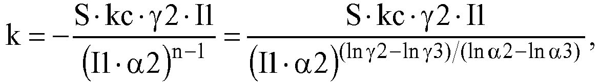
![]()
![]()
![]()
![]()
![]()
![]()
![]()
![]()
![]()
![]()
![]()
![]()
![]()
![]()
Die Bedingung für den Offset 0 ist somit: ![]()

![]()
Dabei ist CS der Spulenfaktor, S die Empfindlichkeit, V1 der Wert des Ausgangssignals V beim ersten Wert I1 des Eingangssignals I, V2 der zweite Wert des Ausgangssignals V beim zweiten Wert 12 des Eingangssignals I, V3 der dritte Wert des Ausgangssignals V beim dritten Wert 13 des Eingangssignals I, IC1 der erste Wert des Spulenstroms, IC2 der zweite Wert des Spulenstroms und IC3 der dritte Wert des Spulenstroms.Where CS is the coil factor, S the sensitivity, V1 the value of the output signal V at the first value I1 of the input signal I, V2 the second value of the output signal V at the
Die iterative Regelschleife weist folgende Elemente auf:
- Der Wert des Spulenstroms IC wird auf einen Startwert Null eingestellt, so dass gilt:

- Die Abarbeitung der Schleife fängt mit folgendem Schleifenanfang an:
- Einstellen des ersten Arbeitspunktes mittels Einstellen des ersten Wertes I1 des Eingangssignals I Speichern des ersten Werts V1 des Ausgangssignals V
- Einstellen des zweiten Arbeitspunktes mittels Einstellen des zweiten
Werts 12 des Eingangssignals I. Der zweiteWert 12 des Eingangssignals I ist dabei um den Faktor α2 größer als der erste Wert I1 des Eingangssignals, so dass gilt:
- Der zweite Wert IC2 des Spulenstroms IC wird nun so eingestellt, dass der zweite Wert V2 des Ausgangssignals V folgende Beziehung erfüllt:

- Dabei wird der Faktor γ2 ermittelt:

- Einstellen des dritten Arbeitspunktes mittels Einstellen des dritten
Werts 13 des Eingangssignals I. Der dritteWert 13 des Eingangssignals I ist dabei um den Faktor α3 größer als der erste Wert I1 des Eingangssignals I, so dass gilt:
- Der dritte Wert IC3 des Spulenstroms IC wird nun so eingestellt, dass der dritte Wert V3 des Ausgangssignals V folgende Beziehung erfüllt:

- Dabei wird der Faktor γ3 ermittelt:

- α2 und α3 sind dabei vorgegebene Werte. Die Werte für γ2 und γ3 werden wie oben angegeben ermittelt. Aus den Werten für α2, α3, γ2 und γ3 kann der Wert des Exponenten n und darauf der Wert des Offsetfaktors k gemäß folgenden Gleichungen errechnet werden:


- Der erste Wert des Spulenstroms IC1 kann nun aus folgender Gleichung berechnet und eingestellt werden. Mit dem Wert IC1 für den Spulenstrom wird die Rest-Offsetspannung VOFF kompensiert.

- Hier wird die Schleife beendet.
- The value of the coil current IC is set to a starting value zero, so that the following applies:
- The execution of the loop begins with the following loop start:
- Setting the first operating point by means of setting the first value I1 of the input signal I. Storing the first value V1 of the output signal V
- Setting the second operating point by means of setting the
second value 12 of the input signal I. Thesecond value 12 of the input signal I is greater than the first value I1 of the input signal by the factor α2, so that the following applies: - The second value IC2 of the coil current IC is now adjusted so that the second value V2 of the output signal V satisfies the following relationship:
- The factor γ2 is determined:
- Setting the third operating point by means of setting the
third value 13 of the input signal I. Thethird value 13 of the input signal I is greater than the first value I1 of the input signal I by the factor α3, so that the following applies: - The third value IC3 of the coil current IC is now set so that the third value V3 of the output signal V satisfies the following relationship:
- The factor γ3 is determined:
- α2 and α3 are given values. The values for γ2 and γ3 are determined as indicated above. From the values for α2, α3, γ2 and γ3, the value of the exponent n and then the value of the offset factor k can be calculated according to the following equations:
- The first value of the coil current IC1 can now be calculated and set from the following equation. With the value IC1 for the coil current, the residual offset voltage VOFF is compensated.
- Here the loop is ended.
Obige Schleife wird mehrfach durchlaufen, bis ein Konvergenzkriterium erfüllt ist.The above loop is run through several times until a convergence criterion is met.
Das Ausgangssignal V des Hallsensors 11 weist somit die logischen Werte Null und Eins auf. Das Magnetfeldsignal SB wird von der Berechnungseinheit 21 bereitgestellt. Ein Kompensationsstrom IK fließt durch die Kompensationsstromquelle 38. Die Kompensationseinheit 37 beseitigt einen Teil des Offsets. Der Bereich für die Werte des Spulenstroms IC kann klein gehalten werden, dadurch dass der Offset mittels der Kompensationseinheit 37 reduziert ist.The output signal V of the
Eine sechste Ausführungsform des Verfahrens wird mit Hilfe der in
Für die sechste Ausführungsform des Verfahrens werden der Wert des Exponenten n und der Wert des Offsetfaktors k wie oben angegeben extrahiert. Ein erster Arbeitspunkt wird eingestellt. Beispielsweise wird der dritte Wert 13 des Eingangssignals von der Signalquelle 12 abgegeben und dem Hallsensor 11 zugeleitet. Der Wert des Spulenstroms IC wird nun so eingestellt, dass der dritte Wert V3 des Ausgangssignals V Null erreicht. Vom Wert des Spulenstroms IC wird nun der Anteil abgezogen, der zur Kompensation des Offsets erforderlich ist. Der übrige Wert des Spulenstroms IC ist somit proportional zum Wert des Magnetfelds B. Daraus lässt sich der Wert des Magnetfelds B berechnen.For the sixth embodiment of the method, the value of the exponent n and the value of the offset factor k are extracted as indicated above. A first operating point is set. For example, the
Der Verstärker 18 weist eine steile Übersetzungskennlinie auf. Eine kleine Änderung des Sensorsignals VS am Eingang des Verstärkers 18 führt zu einer großen Änderung des verstärkten Sensorsignals AV. Die Berechnungseinheit 21 berechnet den Wert des Exponenten n und den Wert des Offsetfaktors k, den Wert der Offsetspannung VOFF oder den Wert des Spulenstroms IC, welcher zur Offsetspannung VOFF korrespondiert. Weiter stellt die Berechnungsschaltung 21 die Nullpunktbedingung durch Einstellen des geeigneten Werts des Spulenstroms IC ein.The
Der Wert des Spulenstroms IC setzt sich gemäß folgender Gleichung aus dem Wert IB, der linear vom Wert des Eingangssignals I abhängt, und dem Wert ICOFF, welcher zur Kompensation der Offsetspannung dient, zusammen: ![]()
![]()
Der Wert IB ist proportional zum Wert des Magnetfelds B. Die Messung des Magnetfelds hängt dann von der Empfindlichkeit S, dem Spulenfaktor CS und dem Wert des Spulenstroms IC ab. Der Wert der Empfindlichkeit S und des Spulenfaktors CS können während eines Produktionstests bestimmt werden. Die Werte können als vorgegebene Parameter während der gesamten Lebensdauer der Hallsensoranordnung 11 verwendet werden. Der Spulenstrom IC weist mit Vorteil einen besseren dynamischen Bereich als der Kanal auf, da der Kanal die Aufgabenstellung zu bewältigen hat, dass die Offsetspannung des Hallelements 14 größer als das Ausgangssignals V aufgrund eines kleinen Wertes des Magnetfelds B ist.The value IB is proportional to the value of the magnetic field B. The measurement of the magnetic field then depends on the sensitivity S, the coil factor CS and the value of the coil current IC. The value of the sensitivity S and the coil factor CS can be determined during a production test. The values may be used as predetermined parameters during the entire life of the
Gemäß dem Verfahren wird bei verschiedenen Werten I1, 12, 13 des Eingangssignals I ein Spulenstrom IC der Spule 30 zugeleitet. Der Spulenstrom IC wird so eingestellt, dass die Nullpunktbedingung vom Hallsensor 11 erreicht wird. Das heißt, dass das Ausgangssignal V näherungsweise Null ist. Der Wert des Spulenstrom IC hängt vom Magnetfeld B und vom restlichen Offset ab, welcher in einem vorangegangenen Iterationsschritt berechnet wurde. Das magnetfeldabhängige Signal IB kann durch Subtraktion des restlichen Offsets vom Wert des Spulenstroms IC berechnet werden. Mit Vorteil ist der Kanal auf einen Nullpunktdetektor reduziert. Vorteilhafterweise ist es nicht notwendig, dass der Verstärker 18 im Kanal eine hohe Linearität der Verstärkungskennlinie aufweist. Mit Vorteil hängt die Messgenauigkeit vor allem vom Digital-Analog-Wandler 33 ab, so dass mit geringem Aufwand eine hohe Genauigkeit erreicht werden kann. Mit Vorteil kann die Kalibration bei einem angelegten externen Magnetfeld mit unbekannter Magnetfeldstärke durchgeführt werden.According to the method, at different values I1, 12, 13 of the input signal I, a coil current IC is fed to the
In einer bevorzugten Ausführungsform wird das Ausgangssignal V nach Durchführung der Current Spinning-Technik bereitgestellt. Der Rest-Offsetwert ist somit bereits gering. Daher sind nur niedrige Werte für den Spulenstrom IC notwendig. Es ist ausreichend, die Spule 30 für geringe Ströme auszulegen.In a preferred embodiment, the output signal V is provided after performing the current spinning technique. The residual offset value is thus already low. Therefore, only low values for the coil current IC are necessary. It is sufficient to design the
In einer Ausführungsform umfasst der Hallsensor 11 zusätzlich zu den in
In einer alternativen, nicht gezeigten Ausführungsform ist die Spule 30 mit dem Hallsensor 11 über einen Strompfad gekoppelt. Dabei kann der Spulenstrom IC zusätzlich auch als Eingangssignal I für das Hallelement 14 eingesetzt werden. Somit kann der Spulenstrom IC als Eingangssignal I durch den Hallsensor 11 fließen. Der Spulenstrom IC fließt sowohl durch die Spule 30 als auch durch das Hallelement 14. Somit wird mit Vorteil ein Stromverbrauch reduziert.In an alternative, not shown embodiment, the
In einer alternativen, nicht gezeigten Ausführungsform umfasst die Hallsensoranordnung 10 einen Temperatursensor. Die Temperatur der Hallsensoranordnung 10 wird mittels des Temperatursensors gemessen. Zur Korrektur ist der Temperaturkoeffizient der Empfindlichkeit S im Speicher 20 gespeichert. Somit kann eine Temperaturkompensation durchgeführt werden.In an alternative, not shown embodiment, the
In einer alternativen, nicht gezeigten Ausführungsform weist der Hallsensor 11 das Hallelement 14 sowie ein weiteres Hallelement auf. Das Hallelement 14 und das weitere Hallelement können gemäß dem Prinzip "Offsetreduktion durch paarweise Zusammenschalten" miteinander verbunden sein.In an alternative, not shown embodiment, the
In einer alternativen Ausführungsform ist der Nullpunktdetektor 41 als Fensterkomparator ausgebildet. Der Fensterkomparator gibt als Ausgangssignal V an, ob das Signal am Eingang des Nullpunktdetektors 41 kleiner als ein unterer Schwellwert, zwischen dem unteren Schwellwert und einem oberen Schwellwert oder größer als der obere Schwellwert ist. Der untere Schwellwert hat einen negativen und der obere Schwellwert einen positiven Wert. Der obere und der untere Schwellwert sind nahe bei 0 Volt.In an alternative embodiment, the zero
Optional kann die Kompensationseinheit 37 weggelassen werden. Der Ausgang der Ausgangsschaltung 16 ist dann direkt an den Eingang des Verstärkers 18 angeschlossen.Optionally, the
Die Spannungsquelle 42 stellt ausgangsseitig eine Versorgungsspannung VD bereit. Die Versorgungsspannung VD wird dem Hallsensor 11 und der Ermittlungseinheit 13 zu deren Spannungsversorgung zugeleitet. Am Bezugspotentialanschluss 36 ist ein Bezugspotential VSS abgreifbar. Am Versorgungsspannungsanschluss 44 liegt eine weitere Versorgungsspannung VDD an. Der vom Stromgenerator 31 bereitgestellte Spulenstrom IC fließt vom Versorgungsspannungsanschluss 44 über den Knoten 43 zum Hallsensor 11 und damit zum Hallelement 14. Die Spannungsquelle 42 dient dabei als Lastausgleich. Mit Vorteil kann somit der Spulenstrom IC teilweise oder vollständig durch das Hallelement 14 fließen. Damit ist der Wirkungsgrad der Hallsensoranordnung 10 erhöht.The
In einer Ausführungsform umfasst der Hallsensor 11 eine erste Anzahl M Hallelemente. Dies ist durch die Anzahl M von Leitungen zwischen dem Knoten 43 und dem Hallelement 14 in
Das Hallelement 14 weist einen ersten, zweiten, dritten und vierten Anschluss 51 bis 54 auf. Das Hallelement 14 ist symmetrisch realisiert. Der erste Anschluss 51 liegt dem dritten Anschluss 53 gegenüber. Entsprechend liegt der zweite Anschluss dem vierten Anschluss 55 gegenüber. Die Eingangsschaltung 15 umfasst einen ersten und einen zweiten Multiplexer 55, 56. Ebenso umfasst die Ausgangsschaltung 16 einen dritten und einen vierten Multiplexer 57, 58. Der erste, zweite, dritte und vierte Multiplexer 55 bis 58 weisen jeweils vier Eingänge auf, die mit dem ersten, zweiten, dritten und vierten Anschluss 51 bis 54 des Hallelements 14 gekoppelt sind. Ein Ausgang des ersten Multiplexers 55 ist an den Bezugspotentialanschluss 36 angeschlossen. Ein Ausgang des zweiten Multiplexers 56 ist über den Eingang des Hallsensors 11 an den Ausgang der Signalquelle 12 angeschlossen. Ein Ausgang des dritten Multiplexers 57 und ein Ausgang des vierten Multiplexers 58 sind mit dem Verstärker 18 gekoppelt. Der Verstärker 18 weist einen ersten und einen zweiten Eingang 59, 60 auf. Der erste Eingang 59 ist an den Ausgang des dritten Multiplexers 57 und der zweite Eingang 60 ist an den Ausgang des vierten Multiplexers 58 angeschlossen.The
Die Stromquelle 32 und die weitere Stromquelle 50 sind jeweils als Konstantstromquellen implementiert. Die Stromquelle 32 und die weitere Stromquelle 50 sind jeweils getrennt einschaltbar und ausschaltbar. Die Stromquelle 32 gibt einen ersten Stromwert IP1 ab, der dem ersten Wert I1 des Eingangssignals I entspricht. Zur Erzeugung des ersten Werts I1 des Eingangssignals I wird somit die Stromquelle 32 eingeschaltet. Die weitere Stromquelle 50 gibt einen zweiten Stromwert IP2 ab. Die Summe aus dem ersten und dem zweiten Stromwert IP1, IP2 entspricht dabei dem zweiten Wert 12 des Eingangssignals I. Zur Erzeugung des zweiten Werts 12 des Eingangssignals I werden somit die Stromquelle 32 und die weitere Stromquelle 50 eingeschaltet. Damit erzeugt die Signalquelle 12 den ersten und den zweiten Wert I1, 12 des Eingangssignals I gemäß der ersten Ausführungsform des Verfahrens.The
Die nicht gezeigte Ermittlungseinheit 13 stellt vier Multiplexersteuersignale S1 bis S4 bereit, die dem ersten, zweiten, dritten und vierten Multiplexer 55 bis 58 zugeleitet werden. Mittels der vier Multiplexer 55 bis 58 wird die Current Spinning-Technik, auch Current Spinning-Verfahren oder Strom-Drehverfahren genannt, implementiert. Ein Zyklus der Current Spinning-Technik weist mindestens zwei Phasen auf. Zwei gegenüberliegende Anschlüsse des Hallelements 14 werden über den ersten und den zweiten Multiplexer 55, 56 mit dem Bezugspotentialanschluss 36 beziehungsweise mit dem Ausgang der Signalquelle 12 gekoppelt. Entsprechend werden die beiden weiteren Anschlüsse des Hallelements 14 über den dritten und den vierten Multiplexer 57, 58 mit dem ersten und dem zweiten Eingang 59, 60 des Verstärkers 18 gekoppelt. Das Hallelement 14 ist für ein Magnetfeld senkrecht zur Oberfläche empfindlich. Das Ausgangssignal V des Hallsensors 11 wird erst nach vollständigem Durchlaufen der Phasen eines Zyklusses der Current Spinning-Technik bereitgestellt. Während der Phasen eines Zykluses der Current Spinning-Technik ist der Wert des Eingangssignals I konstant. Zur Bestimmung des Ausgangssignals V beim ersten Wert I1 des Eingangssignals I werden alle Phasen des Zyklusses gemäß der Current Spinning-Technik durchlaufen. Entsprechend werden für die Ermittlung des Ausgangssignals V bei dem zweiten und/oder dem dritten Wert 12, 13 des Eingangssignals I ebenfalls jeweils die Phasen eines Zyklusses der Current Spinning-Technik vollständig durchlaufen.The
Ein Zyklus kann beispielsweise vier Phasen aufweisen. Mittels der Current Spinning-Technik wird erzielt, dass der Stromfluss im Hallelement 14 vier unterschiedliche Richtungen annimmt. Der Betrag des Sensorsignals VS ist ohne vorhandenem Offset in allen vier Phasen der Current Spinning-Technik gleich. In den vier Phasen eines Zyklusses ist somit jeder der vier Anschlüsse 51 bis 54 des Hallelements 14 phasenweise einmal mit dem Ausgang der Signalquelle 12, dem Bezugspotentialanschluss 36, dem ersten Eingang 59 und dem zweiten Eingang 60 des Verstärkers 18 verbunden.For example, a cycle may have four phases. By means of the current spinning technique it is achieved that the current flow in the
Das Sensorsignal VS ist als differentielles Signal realisiert. Das Sensorsignal VS kann zwischen zwei Anschlüssen des Hallelements 14 abgegriffen werden. Das Sensorsignal VS wird dem ersten und dem zweiten Eingang 59, 60 des Verstärkers 18 zugeführt. Der Verstärker 18 wandelt das Sensorsignal VS in ein verstärktes Sensorsignal AV um. Das verstärkte Sensorsignal AV ist auf das Bezugspotential VSS am Bezugspotentialanschluss 36 bezogen. Bevorzugt wird eine der sechs oben geschilderten Ausführungsformen des Verfahrens nach dem vorgeschlagenen Prinzip zusätzlich zur Current Spinning-Technik durchgeführt. Die Kombination der Current Spinning-Technik und einer der erläuterten sechs Ausführungsformen des Verfahrens bewirkt eine hohe Genauigkeit der Magnetfeldbestimmung. In einer alternativen Ausführungsform entspricht der zweite Stromwert IP2 dem zweiten Wert 12 des Eingangssignals. Zur Erzeugung des ersten und des zweiten Werts I1, 12 des Eingangssignals I werden somit die Stromquelle 32 und die weitere Stromquelle 50 einzeln eingeschaltet.The sensor signal VS is implemented as a differential signal. The sensor signal VS can be tapped between two terminals of the
In einer Weiterbildung der alternativen Ausführungsform werden die Stromquelle 32 und die weitere Stromquelle 50 gleichzeitig eingeschaltet. Die Summe aus dem ersten und dem zweiten Stromwert IP1, IP2 entspricht dabei dem dritten Wert 13 des Eingangssignals I. Somit können effizient mit zwei Stromquellen 32, 50 die drei verschiedenen Werte I1, 12, 13 des Eingangssignals I generiert werden.In a further development of the alternative embodiment, the
In einer alternativen, nicht gezeigten Ausführungsform umfasst die Signalquelle 12 eine zusätzliche Stromquelle, deren Ausgang mit dem Ausgang der Signalquelle 12 verbunden ist. In einer alternativen Ausführungsform umfasst ein Zyklus der Current Spinning-Technik genau zwei Phasen. Dabei ist in einer ersten Phase der erste Anschluss 51 des Hallelements 14 mit dem Bezugspotentialanschluss 36 und der dritte Anschluss 53 des Hallelements 14 mit dem Ausgang der Signalquelle 12 über den ersten beziehungsweise den zweiten Multiplexer 55, 56 gekoppelt. In der zweiten Phase ist der erste Anschluss 51 mit dem Ausgang der Signalquelle 12 und der dritte Anschluss 53 mit dem Bezugspotentialanschluss 36 gekoppelt. Der zweite und der vierte Anschluss 52, 54 des Hallelements 14 sind über den dritten und den vierten Multiplexer 57, 58 in der ersten und der zweiten Phase abwechselnd mit dem ersten beziehungsweise dem zweiten Eingang 59, 60 des Verstärkers 36 gekoppelt. In den zwei Phasen des Zyklusses wird somit die Richtung des durch das Hallelement 14 fließenden Stroms um 180 Winkelgrad gedreht.In an alternative, not shown embodiment, the
In einer alternativen, nicht gezeigten Ausführungsform umfasst das Hallelement 14 weitere Anschlüsse, die mittels der vier Multiplexer 55 bis 58 mit der Signalquelle 12 und dem Verstärker 18 gekoppelt sind. Ein Zyklus zum Betreiben eines derartigen Hallelements 14 kann dabei mehr als vier Phasen aufweisen.In an alternative, not shown embodiment, the
In einer alternativen, nicht gezeigten Ausführungsform koppelt die Eingangsschaltung 15 beziehungsweise die Ausgangsschaltung 16 das Hallelementpaar mit der Signalquelle 12 beziehungsweise dem Verstärker 18. Dabei werden die vier Anschlüsse 62 bis 65 des Hallelementpaars über den ersten, zweiten, dritten und vierten Multiplexer 57 bis 58 mit dem Ausgang der Signalquelle 12, dem Bezugspotentialanschluss 36 sowie dem ersten und dem zweiten Eingang 59, 60 des Verstärkers 18 entsprechend den zwei oder vier Phasen der Current Spinning-Technik verbunden.In an alternative, not shown embodiment, the
Optional kann mindestens ein zusätzliches Hallelement mit dem Hallelement 14 und dem weiteren Hallelement 61 gemäß dem Prinzip des geometrischen Spinning verbunden sein.Optionally, at least one additional Hall element may be connected to the
In einer alternativen, nicht gezeigten Ausführungsform weist der Hallsensor 11 vier Hallelemente 14, 61 auf, die miteinander verbunden sind. Dabei können Stromrichtungen durch die vier Hallelemente die Winkel 0°, 45°, 90° und 135° oder alternativ 0°, 90°, 180° und 270° gegenüber einer Gerade in einer ersten Hauptfläche eines Halbleiterkörpers, auf dem der Hallsensor 11 angeordnet ist, aufweisen.In an alternative, not shown embodiment, the
- 1010
- HallsensoranordnungHall sensor arrangement
- 1111
- HallsensorHall sensor
- 1212
- Signalquellesource
- 1313
- Ermittlungseinheitdetermining unit
- 1414
- HallelementHall element
- 1515
- Eingangsschaltunginput circuit
- 1616
- Ausgangsschaltungoutput circuit
- 1717
- Auswerteschaltungevaluation
- 1818
- Verstärkeramplifier
- 1919
- Steuerschaltungcontrol circuit
- 2020
- SpeicherStorage
- 2121
- Berechnungseinheitcalculation unit
- 2222
- weiterer Speicherfurther memory
- 2323
- Subtrahierersubtractor
- 2424
- Vergleichercomparator
- 2525
- Triggereingangtrigger input
- 3030
- SpuleKitchen sink
- 3131
- Stromgeneratorpower generator
- 3232
- Stromquellepower source
- 3333
- Digital-Analog-WandlerDigital to analog converter
- 3434
- Analog-Digital-WandlerAnalog to digital converter
- 3535
- Referenzquellereference source
- 3636
- BezugspotentialanschlussReference potential terminal
- 3737
- Kompensationseinheitcompensation unit
- 3838
- KompensationsstromquelleCompensation current source
- 4040
- StatussignalausgangStatus Signal Output
- 4141
- NullpunktdetektorZero detector
- 4242
- Spannungsquellevoltage source
- 4343
- Knotennode
- 4444
- VersorgungsspannungsanschlussSupply voltage connection
- 5050
- weitere Stromquelleadditional power source
- 51, 52, 53, 5451, 52, 53, 54
- Anschlussconnection
- 51', 52', 53', 54'51 ', 52', 53 ', 54'
- Anschlussconnection
- 5555
- erster Multiplexerfirst multiplexer
- 5656
- zweiter Multiplexersecond multiplexer
- 5757
- dritter Multiplexerthird multiplexer
- 5858
- vierter Multiplexerfourth multiplexer
- 5959
- erster Eingangfirst entrance
- 6060
- zweiter Eingangsecond entrance
- AVAV
- verstärktes Sensorsignalamplified sensor signal
- BB
- Magnetfeldmagnetic field
- CSCS
- Spulenfaktorcoils factor
- II
- Eingangssignalinput
- ICIC
- Spulenstromcoil current
- IKIK
- Kompensationsstromcompensating current
- IP1IP1
- erster Stromwertfirst current value
- IP2IP2
- zweiter Stromwertsecond current value
- kk
- Offsetfaktoroffset factor
- nn
- Exponentexponent
- SBSB
- Magnetfeldsignalmagnetic field signal
- SISI
- Steuersignalcontrol signal
- SICSIC
- weiteres Steuersignalanother control signal
- STRSTR
- Triggersignaltrigger signal
- STSSTS
- Statussignalstatus signal
- S1, S2, S3, S4S1, S2, S3, S4
- Multiplexersteuersignalemultiplexer
- VV
- Ausgangssignaloutput
- VDVD
- Versorgungsspannungsupply voltage
- VDDVDD
- weitere Versorgungsspannungfurther supply voltage
- VOFFVOFF
- Rest-OffsetspannungResidual offset voltage
- VOFFCVOFFC
- gemessene Offsetspannungmeasured offset voltage
- VOFFRVOFFR
- restliche Offsetspannungresidual offset voltage
- VREFVREF
- Referenzsignalreference signal
- VSVS
- Sensorsignalsensor signal
- α2, α3α2, α3
- Skalierungsfaktorscaling factor
Claims (15)
- A method of operating a Hall sensor assembly, comprising:- setting at least two values (I1, 12), having different absolute magnitudes, of an input signal (I) of a Hall sensor (11) of the Hall sensor assembly (10) and determining the associated values (V1, V2) of an output signal (V) of the Hall sensor (11), the output signal (V) being made available not until having completely run through the phases of a cycle of the Current Spinning Technology and the value of the input signal (I) being constant during the phases of the cycle of the Current Spinning Technology, and- determining a residual offset value (k, VOFF) of the output signal (V) as a function of the values (V1, V2) of the output signal (V), which have been determined with the at least two values (I1, 12) of the input signal (I).
- The method according to claim 1,
in which the input signal (I) is realized as a current or a voltage. - The method according to claim 1 or 2,
in which the at least two values (I1, 12) of the input signal (I) or a scaling factor (α2, α3) between two values of the set of the at least two values (I1, 12) of the input signal (I) are taken into consideration in the determination of the residual offset value (k, VOFF). - The method according to any of the claims 1 to 3,
in which the Hall sensor assembly (10) is calibrated in use, a calibration phase in which the residual offset value (k, VOFF) is determined being interposed between two operation phases in which the value of a magnetic field (B) is determined as a function of the residual offset value (k, VOFF). - The method according to any of the claims 1 to 4,
in which the Hall sensor assembly (10) is calibrated in the presence of an external magnetic field (B) having an unknown magnetic field strength. - The method according to any of the claims 1 to 5,
in which the residual offset value is an offset factor (k) or a residual offset voltage (VOFF), the offset factor (k) and the residual offset voltage (VOFF) being calculated according to the following equation:
wherein VOFF is the value of the residual offset voltage, k is the value of the offset factor, I is the value of the input signal and n is the value of an exponent. - The method according to claim 6,
in which the value of the exponent (n) is predefined. - The method according to claim 6,
in which the value of the exponent (n) is determined by means of setting at least three values (I1, 12), having different absolute magnitudes, of the input signal (I) and determining the associated values (V1, V2, V3) of the output signal (V) of the Hall sensor (11). - The method according to any of the claims 1 to 8,
in which the value of a magnetic field (B) is determined according to the following equation:
wherein V is the value of the output signal, B is the value of the magnetic field, S is the value of a sensitivity, I is the value of the input signal and VOFF is the value of a residual offset voltage. - The method according to claim 9,
in which the value of the sensitivity (S) is predefined or in which a coil (30) is arranged with respect to the Hall sensor (11) in such a way that the magnetic field of the coil (30) has an influence on the magnetic field detected by the Hall sensor (11), and the value of the sensitivity (S) is determined with the at least two values (I1, 12) of the input signal (I) by means of the coil (30). - The method according to any of the claims 1 to 10,
in which a coil (30) is arranged with respect to the Hall sensor (11) in such a way that the magnetic field of the coil (30) has an influence on the magnetic field (B) detected by the Hall sensor (11), and the value of a coil current (IC) is set in an operation phase as a function of the residual offset value (k, VOFF). - The method according to any of the claims 1 to 10,
in which a coil (30) is arranged with respect to the Hall sensor (11) in such a way that the magnetic field of the coil (30) has an influence on the magnetic field (B) detected by the Hall sensor (11), and the value of a coil current (IC) is set in an operation phase in such a way that the output signal (V) approaches zero value. - The method according to claim 12,
in which the coil (30) is coupled to the Hall sensor (11) in such a way that the coil current (IC) flows through the Hall sensor (11) as an input signal (I). - A Hall sensor assembly, comprising:- a Hall sensor (11), comprising- a Hall element (14),- an input circuit (15) connecting an input of the Hall sensor (11) to the Hall element (14),- an output circuit (16) and an evaluation circuit (17) which connect the Hall element (14) to an output of the Hall sensor (11), an output signal (V) provided by the evaluation circuit (17) being made available not until having completely run through the phases of a cycle of the Current Spinning Technology,- a signal source (12) which is coupled to the input of the Hall sensor (11), and- a determination unit (13) which is coupled to the output of the Hall sensor (11),
characterized in that- the signal source (12) is arranged for providing at least two values (I1, 12), having different absolute magnitudes, of an input signal (I) of the Hall sensor (11), with the value of the input signal (I) being constant during the phases of the cycle of the Current Spinning Technology, and- the determination unit (13) is arranged for determining a residual offset value (k, VOFF) of an output signal (V) of the Hall sensor (11) as a function of the values (V1, V2) of the output signal (V), which are determined with the at least two values (I1, 12) of the input signal (I). - The Hall sensor assembly according to claim 14, comprising a coil (30) which is firmly connected to the Hall sensor (11) and arranged with respect to the Hall sensor (11) in such a manner that the magnetic field (B) which can be detected by the Hall sensor (11) can be influenced by the magnetic field of the coil (30).
Applications Claiming Priority (2)
| Application Number | Priority Date | Filing Date | Title |
|---|---|---|---|
| DE102011102483A DE102011102483A1 (en) | 2011-05-24 | 2011-05-24 | Method for operating a Hall sensor arrangement and Hall sensor arrangement |
| PCT/EP2012/059728 WO2012160143A2 (en) | 2011-05-24 | 2012-05-24 | Method for operating a hall sensor assembly, and hall sensor assembly |
Publications (2)
| Publication Number | Publication Date |
|---|---|
| EP2715384A2 EP2715384A2 (en) | 2014-04-09 |
| EP2715384B1 true EP2715384B1 (en) | 2015-07-15 |
Family
ID=46320900
Family Applications (1)
| Application Number | Title | Priority Date | Filing Date |
|---|---|---|---|
| EP12728424.8A Active EP2715384B1 (en) | 2011-05-24 | 2012-05-24 | Method for operating a hall sensor assembly, and hall sensor assembly |
Country Status (4)
| Country | Link |
|---|---|
| US (1) | US9551765B2 (en) |
| EP (1) | EP2715384B1 (en) |
| DE (1) | DE102011102483A1 (en) |
| WO (1) | WO2012160143A2 (en) |
Families Citing this family (45)
| Publication number | Priority date | Publication date | Assignee | Title |
|---|---|---|---|---|
| US9823090B2 (en) | 2014-10-31 | 2017-11-21 | Allegro Microsystems, Llc | Magnetic field sensor for sensing a movement of a target object |
| US9817078B2 (en) | 2012-05-10 | 2017-11-14 | Allegro Microsystems Llc | Methods and apparatus for magnetic sensor having integrated coil |
| GB201217293D0 (en) * | 2012-09-27 | 2012-11-14 | Texas Instruments Deutschland | Improvements on or relating to sensing arrangements |
| US10725100B2 (en) | 2013-03-15 | 2020-07-28 | Allegro Microsystems, Llc | Methods and apparatus for magnetic sensor having an externally accessible coil |
| US10495699B2 (en) * | 2013-07-19 | 2019-12-03 | Allegro Microsystems, Llc | Methods and apparatus for magnetic sensor having an integrated coil or magnet to detect a non-ferromagnetic target |
| US10145908B2 (en) | 2013-07-19 | 2018-12-04 | Allegro Microsystems, Llc | Method and apparatus for magnetic sensor producing a changing magnetic field |
| US9810519B2 (en) | 2013-07-19 | 2017-11-07 | Allegro Microsystems, Llc | Arrangements for magnetic field sensors that act as tooth detectors |
| US9389295B2 (en) * | 2013-09-10 | 2016-07-12 | Fisher Controls International Llc | Hall effect sensor system with diagnostic capabilities |
| GB201319627D0 (en) * | 2013-11-06 | 2013-12-18 | Melexis Technologies Nv | Hall sensor readout system with offset determination using the hall element itself |
| US9720054B2 (en) | 2014-10-31 | 2017-08-01 | Allegro Microsystems, Llc | Magnetic field sensor and electronic circuit that pass amplifier current through a magnetoresistance element |
| US9823092B2 (en) | 2014-10-31 | 2017-11-21 | Allegro Microsystems, Llc | Magnetic field sensor providing a movement detector |
| US9719806B2 (en) | 2014-10-31 | 2017-08-01 | Allegro Microsystems, Llc | Magnetic field sensor for sensing a movement of a ferromagnetic target object |
| US10712403B2 (en) | 2014-10-31 | 2020-07-14 | Allegro Microsystems, Llc | Magnetic field sensor and electronic circuit that pass amplifier current through a magnetoresistance element |
| US10126348B2 (en) * | 2015-04-29 | 2018-11-13 | ZTZ Service International, Inc. | Combined on-line bushing monitoring and geo-magnetic induced current monitoring system |
| US11402440B2 (en) * | 2015-07-17 | 2022-08-02 | Allegro Microsystems, Llc | Methods and apparatus for trimming a magnetic field sensor |
| US10260905B2 (en) | 2016-06-08 | 2019-04-16 | Allegro Microsystems, Llc | Arrangements for magnetic field sensors to cancel offset variations |
| US10012518B2 (en) | 2016-06-08 | 2018-07-03 | Allegro Microsystems, Llc | Magnetic field sensor for sensing a proximity of an object |
| US10041810B2 (en) | 2016-06-08 | 2018-08-07 | Allegro Microsystems, Llc | Arrangements for magnetic field sensors that act as movement detectors |
| DE102016225305B4 (en) * | 2016-12-16 | 2019-07-11 | Fraunhofer-Gesellschaft zur Förderung der angewandten Forschung e.V. | Method for offset compensation of a sensor signal of a Hall sensor and sensor arrangement |
| US10310028B2 (en) | 2017-05-26 | 2019-06-04 | Allegro Microsystems, Llc | Coil actuated pressure sensor |
| US10996289B2 (en) | 2017-05-26 | 2021-05-04 | Allegro Microsystems, Llc | Coil actuated position sensor with reflected magnetic field |
| US10641842B2 (en) | 2017-05-26 | 2020-05-05 | Allegro Microsystems, Llc | Targets for coil actuated position sensors |
| US11428755B2 (en) | 2017-05-26 | 2022-08-30 | Allegro Microsystems, Llc | Coil actuated sensor with sensitivity detection |
| US10837943B2 (en) | 2017-05-26 | 2020-11-17 | Allegro Microsystems, Llc | Magnetic field sensor with error calculation |
| US10324141B2 (en) | 2017-05-26 | 2019-06-18 | Allegro Microsystems, Llc | Packages for coil actuated position sensors |
| JP6620796B2 (en) * | 2017-07-28 | 2019-12-18 | Tdk株式会社 | Offset estimation apparatus and method, magnetic sensor correction apparatus, and current sensor |
| JP2019062450A (en) * | 2017-09-27 | 2019-04-18 | 日本電産株式会社 | Arithmetic circuit, control circuit and display unit posture detection system |
| EP3467443B1 (en) | 2017-10-05 | 2021-08-18 | ams AG | Position sensor and method for position sensing and diagnostic |
| US10866117B2 (en) | 2018-03-01 | 2020-12-15 | Allegro Microsystems, Llc | Magnetic field influence during rotation movement of magnetic target |
| US11255700B2 (en) | 2018-08-06 | 2022-02-22 | Allegro Microsystems, Llc | Magnetic field sensor |
| DE102018128469B4 (en) * | 2018-11-14 | 2020-11-12 | Senis Ag | Magnetic field sensor with low noise and high bandwidth |
| US10732164B2 (en) | 2018-12-12 | 2020-08-04 | ZTZ Service International, Inc. | System and method for headspace monitoring in transformers |
| US10823586B2 (en) | 2018-12-26 | 2020-11-03 | Allegro Microsystems, Llc | Magnetic field sensor having unequally spaced magnetic field sensing elements |
| US11061084B2 (en) | 2019-03-07 | 2021-07-13 | Allegro Microsystems, Llc | Coil actuated pressure sensor and deflectable substrate |
| US10955306B2 (en) | 2019-04-22 | 2021-03-23 | Allegro Microsystems, Llc | Coil actuated pressure sensor and deformable substrate |
| US11061100B2 (en) * | 2019-06-12 | 2021-07-13 | Texas Instruments Incorporated | System for continuous calibration of hall sensors |
| US11867773B2 (en) | 2019-06-18 | 2024-01-09 | Texas Instruments Incorporated | Switched capacitor integrator circuit with reference, offset cancellation and differential to single-ended conversion |
| US11237020B2 (en) | 2019-11-14 | 2022-02-01 | Allegro Microsystems, Llc | Magnetic field sensor having two rows of magnetic field sensing elements for measuring an angle of rotation of a magnet |
| US11280637B2 (en) | 2019-11-14 | 2022-03-22 | Allegro Microsystems, Llc | High performance magnetic angle sensor |
| US11262422B2 (en) | 2020-05-08 | 2022-03-01 | Allegro Microsystems, Llc | Stray-field-immune coil-activated position sensor |
| RU2762021C1 (en) * | 2021-02-16 | 2021-12-14 | Открытое акционерное общество "Севернефтегазпром" | Hall sensor diagnostic system and method for its application |
| US11493361B2 (en) | 2021-02-26 | 2022-11-08 | Allegro Microsystems, Llc | Stray field immune coil-activated sensor |
| US11578997B1 (en) | 2021-08-24 | 2023-02-14 | Allegro Microsystems, Llc | Angle sensor using eddy currents |
| CN114383495B (en) * | 2021-11-15 | 2023-11-03 | 北京诺多科技发展有限公司 | double-Hall yaw angle measurement method |
| US20230236267A1 (en) * | 2022-01-27 | 2023-07-27 | Nxp Usa, Inc. | Sensor calibration circuit |
Family Cites Families (13)
| Publication number | Priority date | Publication date | Assignee | Title |
|---|---|---|---|---|
| DE4302342A1 (en) * | 1992-01-28 | 1993-07-29 | El Mos Elektronik In Mos Techn | Offset compensated measurement of magnetic field with Hall element - involves chip-internal electronic compensation with two measurement phases between which measurement and supply connections are interchanged |
| DE4431703C2 (en) | 1994-09-06 | 1997-01-30 | Itt Ind Gmbh Deutsche | Magnetic field sensor with Hall element |
| JP3835486B2 (en) * | 1996-09-09 | 2006-10-18 | アーエムエス インターナショナル アーゲー | Method for reducing the offset voltage of a hall device |
| US6064202A (en) | 1997-09-09 | 2000-05-16 | Physical Electronics Laboratory | Spinning current method of reducing the offset voltage of a hall device |
| DE19910411C2 (en) * | 1999-03-10 | 2001-08-30 | Daimler Chrysler Ag | Method and device for offset-compensated magnetic field measurement using a Hall sensor |
| DE19943128A1 (en) | 1999-09-09 | 2001-04-12 | Fraunhofer Ges Forschung | Hall sensor arrangement for offset-compensated magnetic field measurement |
| JP4601892B2 (en) | 2002-07-04 | 2010-12-22 | ラムバス・インコーポレーテッド | Semiconductor device and bump manufacturing method of semiconductor chip |
| DE10313642A1 (en) * | 2003-03-26 | 2004-10-14 | Micronas Gmbh | Hall sensor with reduced offset |
| NL1025089C2 (en) * | 2003-12-19 | 2005-06-21 | Xensor Integration B V | Magnetic field sensor, carrier of such a magnetic field sensor and a compass, provided with such a magnetic field sensor. |
| DE102004021863A1 (en) | 2004-05-04 | 2005-12-01 | Infineon Technologies Ag | Sensor element for providing a sensor signal and method for operating a sensor element |
| GB0620307D0 (en) * | 2006-10-16 | 2006-11-22 | Ami Semiconductor Belgium Bvba | Auto-calibration of magnetic sensor |
| DE102007044471A1 (en) * | 2007-09-18 | 2009-04-02 | Fraunhofer-Gesellschaft zur Förderung der angewandten Forschung e.V. | Method for sectionally determining a parameter-dependent correction value approximation course and sensor arrangement |
| US8154281B2 (en) * | 2008-04-17 | 2012-04-10 | Infineon Technologies Ag | Sensor system wherein spinning phases of the spinning current hall sensor are lengthened in residual offset adjustment |
-
2011
- 2011-05-24 DE DE102011102483A patent/DE102011102483A1/en not_active Withdrawn
-
2012
- 2012-05-24 WO PCT/EP2012/059728 patent/WO2012160143A2/en active Application Filing
- 2012-05-24 US US14/119,183 patent/US9551765B2/en active Active
- 2012-05-24 EP EP12728424.8A patent/EP2715384B1/en active Active
Also Published As
| Publication number | Publication date |
|---|---|
| US9551765B2 (en) | 2017-01-24 |
| US20140163911A1 (en) | 2014-06-12 |
| DE102011102483A1 (en) | 2012-11-29 |
| WO2012160143A3 (en) | 2013-03-28 |
| EP2715384A2 (en) | 2014-04-09 |
| WO2012160143A2 (en) | 2012-11-29 |
Similar Documents
| Publication | Publication Date | Title |
|---|---|---|
| EP2715384B1 (en) | Method for operating a hall sensor assembly, and hall sensor assembly | |
| DE112012005548B4 (en) | Output value correction method for a physical quantity sensor device, output correction method for a physical quantity sensor, physical quantity sensor device and output value correction device for a physical quantity sensor | |
| EP2567223B1 (en) | Apparatus for measuring the electrical conductivity of a liquid medium | |
| DE102017212837B4 (en) | Circuits and methods for extracting an average load current in switching DC-DC converters | |
| DE10131229B4 (en) | A physical size sensing sensor | |
| DE102005045635B4 (en) | Arrangement and method for providing a temperature-dependent signal | |
| DE102014107504B4 (en) | INPUT LEVEL FOR TEMPERATURE MEASURING SYSTEM | |
| DE102007047887A1 (en) | Capacity detection device | |
| DE102014107499A1 (en) | Calibrated temperature measuring system | |
| EP1636599A1 (en) | Potentiostatic circuit arrangement on a biosensor for digitisation of the measured current | |
| EP1616174B1 (en) | Method for operating a gas sensor | |
| DE102010028718A1 (en) | Detection of a dielectric object | |
| EP2666023A1 (en) | Current measuring device | |
| DE10204652B4 (en) | Circuit arrangement, electrochemical sensor, sensor arrangement and method for processing a current signal provided via a sensor electrode | |
| DE102015002123B4 (en) | Magnetic field detection device | |
| DE3642771A1 (en) | METHOD AND DEVICE FOR MEASURING THE MEASURING SIZE OF A MEASURING OBJECT | |
| EP1599737A1 (en) | Method and circuit arrangement for determining an electric measurement value for a resistance element, preferably for determining an electric current that flows through said resistance element | |
| EP1512021B1 (en) | Circuit configuration and method for compensating for the changes in a transfer ratio of a magnetic field sensor arrangement | |
| EP2233890A2 (en) | Capacitive sensor and method for capacitive recording the distance of an object | |
| DE102006014042A1 (en) | An analog-to-digital conversion device and detection device having the same | |
| DE19947301C1 (en) | Current sensor calibration device for vehicles has controller connected via data lines to sensors, switch for second voltage source, second source itself and switch for constant current sink | |
| EP2174146B1 (en) | Arrangement and method for measuring a current flowing in an electrical conductor | |
| DE102011103790A1 (en) | Self-correcting electronic sensor | |
| EP1744153B1 (en) | Signal transmission device for a measuring probe and method for doing the same. | |
| WO2016005015A1 (en) | Controller and method for minimizing scale factor errors of a rotation rate sensor |
Legal Events
| Date | Code | Title | Description |
|---|---|---|---|
| PUAI | Public reference made under article 153(3) epc to a published international application that has entered the european phase |
Free format text: ORIGINAL CODE: 0009012 |
|
| 17P | Request for examination filed |
Effective date: 20131022 |
|
| AK | Designated contracting states |
Kind code of ref document: A2 Designated state(s): AL AT BE BG CH CY CZ DE DK EE ES FI FR GB GR HR HU IE IS IT LI LT LU LV MC MK MT NL NO PL PT RO RS SE SI SK SM TR |
|
| DAX | Request for extension of the european patent (deleted) | ||
| GRAP | Despatch of communication of intention to grant a patent |
Free format text: ORIGINAL CODE: EPIDOSNIGR1 |
|
| INTG | Intention to grant announced |
Effective date: 20150213 |
|
| GRAS | Grant fee paid |
Free format text: ORIGINAL CODE: EPIDOSNIGR3 |
|
| GRAA | (expected) grant |
Free format text: ORIGINAL CODE: 0009210 |
|
| AK | Designated contracting states |
Kind code of ref document: B1 Designated state(s): AL AT BE BG CH CY CZ DE DK EE ES FI FR GB GR HR HU IE IS IT LI LT LU LV MC MK MT NL NO PL PT RO RS SE SI SK SM TR |
|
| REG | Reference to a national code |
Ref country code: CH Ref legal event code: EP Ref country code: GB Ref legal event code: FG4D Free format text: NOT ENGLISH |
|
| REG | Reference to a national code |
Ref country code: IE Ref legal event code: FG4D Free format text: LANGUAGE OF EP DOCUMENT: GERMAN |
|
| REG | Reference to a national code |
Ref country code: AT Ref legal event code: REF Ref document number: 737072 Country of ref document: AT Kind code of ref document: T Effective date: 20150815 |
|
| REG | Reference to a national code |
Ref country code: DE Ref legal event code: R096 Ref document number: 502012003815 Country of ref document: DE |
|
| REG | Reference to a national code |
Ref country code: NL Ref legal event code: MP Effective date: 20150715 |
|
| REG | Reference to a national code |
Ref country code: LT Ref legal event code: MG4D |
|
| PG25 | Lapsed in a contracting state [announced via postgrant information from national office to epo] |
Ref country code: NO Free format text: LAPSE BECAUSE OF FAILURE TO SUBMIT A TRANSLATION OF THE DESCRIPTION OR TO PAY THE FEE WITHIN THE PRESCRIBED TIME-LIMIT Effective date: 20151015 Ref country code: GR Free format text: LAPSE BECAUSE OF FAILURE TO SUBMIT A TRANSLATION OF THE DESCRIPTION OR TO PAY THE FEE WITHIN THE PRESCRIBED TIME-LIMIT Effective date: 20151016 Ref country code: LT Free format text: LAPSE BECAUSE OF FAILURE TO SUBMIT A TRANSLATION OF THE DESCRIPTION OR TO PAY THE FEE WITHIN THE PRESCRIBED TIME-LIMIT Effective date: 20150715 Ref country code: FI Free format text: LAPSE BECAUSE OF FAILURE TO SUBMIT A TRANSLATION OF THE DESCRIPTION OR TO PAY THE FEE WITHIN THE PRESCRIBED TIME-LIMIT Effective date: 20150715 Ref country code: LV Free format text: LAPSE BECAUSE OF FAILURE TO SUBMIT A TRANSLATION OF THE DESCRIPTION OR TO PAY THE FEE WITHIN THE PRESCRIBED TIME-LIMIT Effective date: 20150715 |
|
| PG25 | Lapsed in a contracting state [announced via postgrant information from national office to epo] |
Ref country code: PL Free format text: LAPSE BECAUSE OF FAILURE TO SUBMIT A TRANSLATION OF THE DESCRIPTION OR TO PAY THE FEE WITHIN THE PRESCRIBED TIME-LIMIT Effective date: 20150715 Ref country code: ES Free format text: LAPSE BECAUSE OF FAILURE TO SUBMIT A TRANSLATION OF THE DESCRIPTION OR TO PAY THE FEE WITHIN THE PRESCRIBED TIME-LIMIT Effective date: 20150715 Ref country code: RS Free format text: LAPSE BECAUSE OF FAILURE TO SUBMIT A TRANSLATION OF THE DESCRIPTION OR TO PAY THE FEE WITHIN THE PRESCRIBED TIME-LIMIT Effective date: 20150715 Ref country code: HR Free format text: LAPSE BECAUSE OF FAILURE TO SUBMIT A TRANSLATION OF THE DESCRIPTION OR TO PAY THE FEE WITHIN THE PRESCRIBED TIME-LIMIT Effective date: 20150715 Ref country code: PT Free format text: LAPSE BECAUSE OF FAILURE TO SUBMIT A TRANSLATION OF THE DESCRIPTION OR TO PAY THE FEE WITHIN THE PRESCRIBED TIME-LIMIT Effective date: 20151116 Ref country code: SE Free format text: LAPSE BECAUSE OF FAILURE TO SUBMIT A TRANSLATION OF THE DESCRIPTION OR TO PAY THE FEE WITHIN THE PRESCRIBED TIME-LIMIT Effective date: 20150715 |
|
| REG | Reference to a national code |
Ref country code: DE Ref legal event code: R097 Ref document number: 502012003815 Country of ref document: DE |
|
| PG25 | Lapsed in a contracting state [announced via postgrant information from national office to epo] |
Ref country code: CZ Free format text: LAPSE BECAUSE OF FAILURE TO SUBMIT A TRANSLATION OF THE DESCRIPTION OR TO PAY THE FEE WITHIN THE PRESCRIBED TIME-LIMIT Effective date: 20150715 Ref country code: DK Free format text: LAPSE BECAUSE OF FAILURE TO SUBMIT A TRANSLATION OF THE DESCRIPTION OR TO PAY THE FEE WITHIN THE PRESCRIBED TIME-LIMIT Effective date: 20150715 Ref country code: SK Free format text: LAPSE BECAUSE OF FAILURE TO SUBMIT A TRANSLATION OF THE DESCRIPTION OR TO PAY THE FEE WITHIN THE PRESCRIBED TIME-LIMIT Effective date: 20150715 Ref country code: EE Free format text: LAPSE BECAUSE OF FAILURE TO SUBMIT A TRANSLATION OF THE DESCRIPTION OR TO PAY THE FEE WITHIN THE PRESCRIBED TIME-LIMIT Effective date: 20150715 Ref country code: IT Free format text: LAPSE BECAUSE OF FAILURE TO SUBMIT A TRANSLATION OF THE DESCRIPTION OR TO PAY THE FEE WITHIN THE PRESCRIBED TIME-LIMIT Effective date: 20150715 |
|
| PLBE | No opposition filed within time limit |
Free format text: ORIGINAL CODE: 0009261 |
|
| STAA | Information on the status of an ep patent application or granted ep patent |
Free format text: STATUS: NO OPPOSITION FILED WITHIN TIME LIMIT |
|
| PG25 | Lapsed in a contracting state [announced via postgrant information from national office to epo] |
Ref country code: RO Free format text: LAPSE BECAUSE OF FAILURE TO SUBMIT A TRANSLATION OF THE DESCRIPTION OR TO PAY THE FEE WITHIN THE PRESCRIBED TIME-LIMIT Effective date: 20150715 |
|
| 26N | No opposition filed |
Effective date: 20160418 |
|
| PG25 | Lapsed in a contracting state [announced via postgrant information from national office to epo] |
Ref country code: IS Free format text: LAPSE BECAUSE OF FAILURE TO SUBMIT A TRANSLATION OF THE DESCRIPTION OR TO PAY THE FEE WITHIN THE PRESCRIBED TIME-LIMIT Effective date: 20150715 |
|
| PG25 | Lapsed in a contracting state [announced via postgrant information from national office to epo] |
Ref country code: SI Free format text: LAPSE BECAUSE OF FAILURE TO SUBMIT A TRANSLATION OF THE DESCRIPTION OR TO PAY THE FEE WITHIN THE PRESCRIBED TIME-LIMIT Effective date: 20150715 Ref country code: BE Free format text: LAPSE BECAUSE OF NON-PAYMENT OF DUE FEES Effective date: 20160531 |
|
| PG25 | Lapsed in a contracting state [announced via postgrant information from national office to epo] |
Ref country code: LU Free format text: LAPSE BECAUSE OF FAILURE TO SUBMIT A TRANSLATION OF THE DESCRIPTION OR TO PAY THE FEE WITHIN THE PRESCRIBED TIME-LIMIT Effective date: 20160524 |
|
| REG | Reference to a national code |
Ref country code: CH Ref legal event code: PL |
|
| GBPC | Gb: european patent ceased through non-payment of renewal fee |
Effective date: 20160524 |
|
| PG25 | Lapsed in a contracting state [announced via postgrant information from national office to epo] |
Ref country code: LI Free format text: LAPSE BECAUSE OF NON-PAYMENT OF DUE FEES Effective date: 20160531 Ref country code: CH Free format text: LAPSE BECAUSE OF NON-PAYMENT OF DUE FEES Effective date: 20160531 |
|
| REG | Reference to a national code |
Ref country code: IE Ref legal event code: MM4A |
|
| REG | Reference to a national code |
Ref country code: FR Ref legal event code: ST Effective date: 20170131 |
|
| PG25 | Lapsed in a contracting state [announced via postgrant information from national office to epo] |
Ref country code: FR Free format text: LAPSE BECAUSE OF NON-PAYMENT OF DUE FEES Effective date: 20160531 |
|
| PG25 | Lapsed in a contracting state [announced via postgrant information from national office to epo] |
Ref country code: IE Free format text: LAPSE BECAUSE OF NON-PAYMENT OF DUE FEES Effective date: 20160524 Ref country code: GB Free format text: LAPSE BECAUSE OF NON-PAYMENT OF DUE FEES Effective date: 20160524 |
|
| PG25 | Lapsed in a contracting state [announced via postgrant information from national office to epo] |
Ref country code: NL Free format text: LAPSE BECAUSE OF FAILURE TO SUBMIT A TRANSLATION OF THE DESCRIPTION OR TO PAY THE FEE WITHIN THE PRESCRIBED TIME-LIMIT Effective date: 20150715 |
|
| PG25 | Lapsed in a contracting state [announced via postgrant information from national office to epo] |
Ref country code: CY Free format text: LAPSE BECAUSE OF FAILURE TO SUBMIT A TRANSLATION OF THE DESCRIPTION OR TO PAY THE FEE WITHIN THE PRESCRIBED TIME-LIMIT Effective date: 20150715 Ref country code: HU Free format text: LAPSE BECAUSE OF FAILURE TO SUBMIT A TRANSLATION OF THE DESCRIPTION OR TO PAY THE FEE WITHIN THE PRESCRIBED TIME-LIMIT; INVALID AB INITIO Effective date: 20120524 Ref country code: SM Free format text: LAPSE BECAUSE OF FAILURE TO SUBMIT A TRANSLATION OF THE DESCRIPTION OR TO PAY THE FEE WITHIN THE PRESCRIBED TIME-LIMIT Effective date: 20150715 |
|
| PG25 | Lapsed in a contracting state [announced via postgrant information from national office to epo] |
Ref country code: TR Free format text: LAPSE BECAUSE OF FAILURE TO SUBMIT A TRANSLATION OF THE DESCRIPTION OR TO PAY THE FEE WITHIN THE PRESCRIBED TIME-LIMIT Effective date: 20150715 Ref country code: MT Free format text: LAPSE BECAUSE OF FAILURE TO SUBMIT A TRANSLATION OF THE DESCRIPTION OR TO PAY THE FEE WITHIN THE PRESCRIBED TIME-LIMIT Effective date: 20150715 Ref country code: MC Free format text: LAPSE BECAUSE OF FAILURE TO SUBMIT A TRANSLATION OF THE DESCRIPTION OR TO PAY THE FEE WITHIN THE PRESCRIBED TIME-LIMIT Effective date: 20150715 Ref country code: MK Free format text: LAPSE BECAUSE OF FAILURE TO SUBMIT A TRANSLATION OF THE DESCRIPTION OR TO PAY THE FEE WITHIN THE PRESCRIBED TIME-LIMIT Effective date: 20150715 |
|
| REG | Reference to a national code |
Ref country code: AT Ref legal event code: MM01 Ref document number: 737072 Country of ref document: AT Kind code of ref document: T Effective date: 20170524 |
|
| PG25 | Lapsed in a contracting state [announced via postgrant information from national office to epo] |
Ref country code: BG Free format text: LAPSE BECAUSE OF FAILURE TO SUBMIT A TRANSLATION OF THE DESCRIPTION OR TO PAY THE FEE WITHIN THE PRESCRIBED TIME-LIMIT Effective date: 20150715 |
|
| PG25 | Lapsed in a contracting state [announced via postgrant information from national office to epo] |
Ref country code: AT Free format text: LAPSE BECAUSE OF NON-PAYMENT OF DUE FEES Effective date: 20170524 |
|
| PG25 | Lapsed in a contracting state [announced via postgrant information from national office to epo] |
Ref country code: AL Free format text: LAPSE BECAUSE OF FAILURE TO SUBMIT A TRANSLATION OF THE DESCRIPTION OR TO PAY THE FEE WITHIN THE PRESCRIBED TIME-LIMIT Effective date: 20150715 |
|
| PGFP | Annual fee paid to national office [announced via postgrant information from national office to epo] |
Ref country code: DE Payment date: 20230519 Year of fee payment: 12 |
|
| P01 | Opt-out of the competence of the unified patent court (upc) registered |
Effective date: 20230822 |