EP2233890A2 - Capacitive sensor and method for capacitive recording the distance of an object - Google Patents
Capacitive sensor and method for capacitive recording the distance of an object Download PDFInfo
- Publication number
- EP2233890A2 EP2233890A2 EP10405024A EP10405024A EP2233890A2 EP 2233890 A2 EP2233890 A2 EP 2233890A2 EP 10405024 A EP10405024 A EP 10405024A EP 10405024 A EP10405024 A EP 10405024A EP 2233890 A2 EP2233890 A2 EP 2233890A2
- Authority
- EP
- European Patent Office
- Prior art keywords
- operational amplifier
- capacitor
- measuring
- capacitance
- inverting
- Prior art date
- Legal status (The legal status is an assumption and is not a legal conclusion. Google has not performed a legal analysis and makes no representation as to the accuracy of the status listed.)
- Withdrawn
Links
Images


Classifications
-
- G—PHYSICS
- G01—MEASURING; TESTING
- G01D—MEASURING NOT SPECIALLY ADAPTED FOR A SPECIFIC VARIABLE; ARRANGEMENTS FOR MEASURING TWO OR MORE VARIABLES NOT COVERED IN A SINGLE OTHER SUBCLASS; TARIFF METERING APPARATUS; MEASURING OR TESTING NOT OTHERWISE PROVIDED FOR
- G01D5/00—Mechanical means for transferring the output of a sensing member; Means for converting the output of a sensing member to another variable where the form or nature of the sensing member does not constrain the means for converting; Transducers not specially adapted for a specific variable
- G01D5/12—Mechanical means for transferring the output of a sensing member; Means for converting the output of a sensing member to another variable where the form or nature of the sensing member does not constrain the means for converting; Transducers not specially adapted for a specific variable using electric or magnetic means
- G01D5/14—Mechanical means for transferring the output of a sensing member; Means for converting the output of a sensing member to another variable where the form or nature of the sensing member does not constrain the means for converting; Transducers not specially adapted for a specific variable using electric or magnetic means influencing the magnitude of a current or voltage
- G01D5/24—Mechanical means for transferring the output of a sensing member; Means for converting the output of a sensing member to another variable where the form or nature of the sensing member does not constrain the means for converting; Transducers not specially adapted for a specific variable using electric or magnetic means influencing the magnitude of a current or voltage by varying capacitance
Definitions
- the invention relates to a capacitive sensor and a method for capacitive detection of an object distance according to the features of patent claims 1 and 8.
- Capacitive proximity switches are widely used in process and automation technology for detecting electrically conductive or non-conductive objects, for example for detecting moving machine parts or filling levels in containers.
- this measuring capacity is part of an oscillator, eg an RC oscillator.
- the oscillation condition of this oscillator is only fulfilled if the value of the measuring capacity exceeds a minimum value due to external influences (approximation of the measuring object).
- the switching state of the sensor output depends on the oscillation amplitude of the oscillator. As soon as this oscillation amplitude exceeds a predetermined or predefinable value, the switching state of the sensor output changes.
- a switching distance can eg by means of a Potentiometer as adjusting the resonant frequency of the oscillator or alternatively the reference voltage for the comparison of the oscillation amplitude can be changed.
- the oscillation amplitude could also be detected and processed further by means of analog or digital signal processing.
- this requires relatively complex electronic circuits with a correspondingly high space requirement.
- reaction time for oscillatory solutions is relatively long. This is especially true if in addition analog-to-digital converters are used to digitize analog measurement signals for further processing.
- a capacitance measuring circuit in which a measuring capacity is detected with the inclusion of a sigma-delta converter.
- the measuring capacitance is clocked via a switch with a reference voltage source and then connected to a passive network, in each case a charge transfer to the passive network takes place. As soon as the charge exceeds a threshold, it is reduced by a predetermined amount and the process is repeated.
- a digital signal in the form of a bit stream is generated as a function of the measuring capacity and the passive network. This bitstream is converted by a filter to a desired output.
- parasitic capacitances and common-mode voltages can lead to errors in the measurement result.
- different operating voltages can cause measurement errors.
- An object of the present invention is to provide a capacitive sensor and a method for easily and accurately detecting a measuring capacity.
- the inventive capacitive sensor comprises an integrated electronic circuit with a delta-sigma converter in fully differential design.
- the electronic circuit is preferably formed on a single chip as an application-specific integrated electronic circuit, called ASIC for short.
- the outputs of the operational amplifier are connected to a system clock-triggered triggering device for generating a bitstream, this bitstream having a mean value reciprocal to the measuring capacitance.
- a measuring capacitor whose measuring capacity is variable by external influences, and a reference capacitor with a fixed reference capacitance are connected to input interfaces or inputs of the integrated circuit.
- the measuring capacitor and / or the reference capacitor could also be integrated into the electronic circuit.
- Both the measuring capacitor and the reference capacitor each one of the electrodes is connected to the ground potential or to a fixed reference potential.
- the respective other electrodes can be connected via a switching device to the non-inverting and the inverting input of the operational amplifier.
- the switching device is controlled by an electronic control unit and includes Switching elements or switches, which are closed and opened depending on the initial state of the triggering device.
- the control electronics are preferably partially or fully integrated in the electronic circuit, which also includes the delta-sigma converter.
- the electronic circuit comprises further input interfaces for compensation capacitances, which correspond to the parasitic capacitances of the reference capacitor and of the measuring capacitor. These input interfaces are also connectable via the switching device with the inverting and the non-inverting input of the operational amplifier.
- the four inputs are connected in a four-phase operation in an order prescribed for each of these inputs respectively with the inverting and the non-inverting input of the operational amplifier and with two different fixed potentials (ground potential and operating voltage potential).
- the phase change is triggered by the system clock.
- the inverting input and the non-inverting input of the operational amplifier are alternately connected during each two of the four phases with the common-mode potential of the operational amplifier.
- the voltage difference between the two outputs of the operational amplifier are respectively incremented or decremented by specific voltage values with each pass of a four-phase cycle, depending on the output state of the trigger device .
- These voltage values are only dependent on the measuring capacitance, the reference capacitance, the integration capacitances and the operating voltage, but not on the common-mode voltage and parasitic capacitances. Faults or errors of the measurement result due to circuit-related parasitic capacitances and due to the common-mode voltage of the operational amplifier are thus eliminated in the inventive capacitive sensor.
- the two integration capacities are specified with identical value. In this case, the average voltage at the output of the electronic circuit adjusts itself to a mean voltage value which is inversely proportional to the measuring capacity.
- FIG. 1 shows a simplified first circuit arrangement for detecting the measuring capacitance C S of a measuring capacitor 1.
- the measuring capacitor 1 and a reference capacitor 3 with a reference capacitance C R are connected via a switching device to the inverting and the non-inverting input of a fully differential operational amplifier 7.
- the switching device comprises a plurality of switching elements or electronic switches 5, which are framed by a thin dotted line 5a.
- a first integration capacitor 9 is arranged with a first integration capacitance C I01 .
- a second integration capacitor 11 having a second integration capacitance C I23 is arranged in a feedback branch between the positive output and the inverting input of the operational amplifier 7.
- the inverting and the non-inverting input of the operational amplifier 7 are connected to the common-mode potential.
- the outputs of the operational amplifier 7 are connected to the inputs of a triggered by a system clock (clock) trigger device 15.
- the switch 13 and the switch 5 are controlled by a (not shown) control electronics.
- the control electronics can be arranged partially or completely together with the circuit arrangement on a common chip. Alternatively, the control electronics can also be designed as a separate part and connected to the integrated circuit on a chip.
- the control electronics can also be designed to perform other tasks, eg for providing a stabilized voltage V DD , for generating the system clock and / or for further processing of the signals at the output of the trigger device 15 (point " D ").
- Two switches 5 framed by a bold broken line 5b are controllable by the control electronics as a function of the initial state of the triggering device 15.
- These switches 5 are designed to interrupt the connection between the measuring capacitor 1 and the inverting or the non-inverting input of the operational amplifier 7 and to close again. They are closed when the signal level V DD (also referred to as "V H " or “H”) is at point D; they are open when the signal level at point D is "V L " or "L".
- V DD also referred to as "V H " or "H”
- V L the signal level at point D is "V L " or "L”.
- the connections to the Reference capacitor 3 is interrupted in an analogous manner and closed again.
- the other two switches 5 in FIG. 1 are switched by the control electronics in the system clock.
- the inputs of the circuit arrangement, to which the measuring capacitor 1 and the reference capacitor 3 are connected connected in a four-phase cycle with the inverting and the non-inverting input of the operational amplifier 7 and with V L and V H.
- the sequence of the individual connections corresponds to that of FIG. 2 illustrated extended embodiment.
- the circuit arrangement comprises a first compensation input, which is designed analogously to the sensor input and likewise has an at least approximately equal parasitic capacitance C PS .
- no measuring capacitor 1 is connected to the first compensation input.
- the first compensation input is analogous to the measuring input via switch 5 of the switching device 5a connectable to the inputs of the operational amplifier 7 and to V L and V H , the connections to the operational amplifier 7 being interruptible by the control electronics as a function of the initial state of the trigger device 15.
- the circuit arrangement comprises a second compensation input, which is designed analogously to the reference input and likewise has an at least approximately equal parasitic capacitance C PR .
- no reference capacitor 3 is connected to the second compensation input.
- FIG. 3 shows a diagram in which the timing of the system clock (Clock) and the dependent phase clocks ⁇ 0 , ⁇ 1 , ⁇ 2 , ⁇ 3 , ⁇ 2 + ⁇ 3 and ⁇ 0 + ⁇ 1 are shown.
- I + non-inverting input of the operational amplifier 7
- I- inverting input of the operational amplifier 7
- V L reference potential (ground)
- D can have the values 0 or 1, depending on whether the output of the triggering device is 15 V L or V H and, correspondingly, the switches 5 framed by the line 5b are opened or closed.
- FIGS. 4 to 7 Simplify the configurations during the individual clock phases for a simplified circuit without parasitic capacitances, as in FIG. 1 is shown. For better clarity, the triggering device 15 is not shown in each case.
- V C S ( ⁇ ) at the measurement capacitor 1, V C R ( ⁇ ) are set forth for the individual phases at the reference capacitor 3, V C I 01 ( ⁇ ) at the first integration capacity 9, V c I 23 ( ⁇ ) at the second integration capacitance and V out ( ⁇ ) between the outputs of the operational amplifier 7.
- the time scale (2 ⁇ s / unit) is the same for all curves K1 to K4.
- the voltage scales at curves K2, K3 and K4 are given in V / unit or mV / unit.
- the values of the measuring capacity CS are 1.12pF at FIG. 8 ; 560fF at FIG. 9 ; 280fF at FIG. 10 and 140fF at FIG. 11 ,
- the output signal (D) of the triggering device 15 consists of square-wave signals, each during four System clocks (clock) or during a 4-phase cycle have the potential V H and follow one another at a time interval which is inversely proportional to the measuring capacitance C S.
- this signal can be output as a pulse-width-modulated distance signal.
- the signal can also be further processed digitally, wherein the time intervals of successive pulses are evaluated.
- the transfer function or the characteristic of the sensor can be specified individually.
- the capacitive sensor can be generated from the output signal of the trigger device 15, for example by a downstream filter in a simple manner, an at least approximately - linearized function of the sensor to be detected object distance or the reciprocal of the measuring capacitance C s represents.
- the values of the integration capacitances C I01 and C I23 and the reference capacitance C R can be determined depending on the desired measuring range and / or the required resolution or accuracy of the sensor.
- each of the integration capacitances C I01 and C I23 can be varied, for example, by the control electronics, in that two or more capacitors are connected in parallel by electronic switches and together Integrating capacity C I01 or C I23 form.
- the value of the externally connected to the chip reference capacitance C R can be changed and adapted to the respective requirements.
- capacitive analog distance sensors it is also possible to design proximity switches or any other sensors in which a capacitance must be detected in the manner according to the invention.
- the output of the sensor behaves at least approximately proportional to the distance of the target, and the sensitivity and accuracy of the sensor are maintained up to greater distances.
- the measuring range is not limited primarily by the sensitivity decreasing with increasing distance (change of the output variable per millimeter change in distance), but by the signal-to-noise ratio, which deteriorates with increasing distance. Since no ideal plate capacitors are used in practice, field distortions at the edge of the electrodes can cause slight deviations of the output characteristic, which indicates the dependence of the measured quantity 1 / C on the target distance.
- the pulse density of the output signal i.e., the number of pulses per unit of time
- increases with increasing distance which at larger distances can result in a larger measurement bandwidth and thus a shorter sensor response time.
Abstract
Description
Gegenstand der Erfindung ist ein kapazitiver Sensor und ein Verfahren zur kapazitiven Erfassung eines Objektabstandes gemäss den Merkmalen der Patentansprüche 1 und 8.The invention relates to a capacitive sensor and a method for capacitive detection of an object distance according to the features of
Kapazitive Näherungsschalter werden in der Prozess- und Automatisierungstechnik verbreitet zum Erfassen von elektrisch leitenden oder nicht leitenden Objekten eingesetzt, z.B. zum Erfassen von sich bewegenden Maschinenteilen oder Füllständen in Behältern. Beim Annähern des zu erfassenden Objekts an den Sensor ändert sich der Wert einer Messkapazität des Sensors. In der Regel ist diese Messkapazität Bestandteil eines Oszillators, z.B. eines RC-Oszillators. Die Schwingungsbedingung dieses Oszillators ist nur dann erfüllt, wenn der Wert der Messkapazität aufgrund äusserer Einflüsse (Annäherung des Messobjektes) einen Minimalwert überschreitet. Der Schaltzustand des Sensorausgangs ist abhängig von der Schwingungsamplitude des Oszillators. Sobald diese Schwingungsamplitude einen vorgegebenen oder vorgebbaren Wert überschreitet, ändert sich der Schaltzustand des Sensorausgangs. Zum Einstellen bzw. Vorgeben eines Schaltabstandes kann z.B. mittels eines Potentiometers als Einstellmittel die Resonanzfrequenz des Oszillators oder alternativ die Referenzspannung für den Vergleich der Schwingungsamplitude verändert werden.Capacitive proximity switches are widely used in process and automation technology for detecting electrically conductive or non-conductive objects, for example for detecting moving machine parts or filling levels in containers. When approaching the object to be detected to the sensor, the value of a measuring capacity of the sensor changes. As a rule, this measuring capacity is part of an oscillator, eg an RC oscillator. The oscillation condition of this oscillator is only fulfilled if the value of the measuring capacity exceeds a minimum value due to external influences (approximation of the measuring object). The switching state of the sensor output depends on the oscillation amplitude of the oscillator. As soon as this oscillation amplitude exceeds a predetermined or predefinable value, the switching state of the sensor output changes. To set or specify a switching distance can eg by means of a Potentiometer as adjusting the resonant frequency of the oscillator or alternatively the reference voltage for the comparison of the oscillation amplitude can be changed.
Grundsätzlich könnte auch die Schwingungsamplitude erfasst und mittels analoger oder digitaler Signalverarbeitung weiter bearbeitet werden. Dies erfordert aber relativ aufwändige elektronische Schaltungen mit entsprechend hohem Platzbedarf.In principle, the oscillation amplitude could also be detected and processed further by means of analog or digital signal processing. However, this requires relatively complex electronic circuits with a correspondingly high space requirement.
Die Messkapazität und damit auch die Schwingungsamplitude nehmen mit zunehmendem Objektabstand stark ab, wobei die Beziehung zwischen Objektabstand und Schwingungsamplitude nicht linear ist. Entsprechend sind Auflösung und Genauigkeit des Sensors mit zunehmendem Objektabstand geringer.The measuring capacity and thus also the oscillation amplitude decrease sharply with increasing object distance, wherein the relationship between object distance and oscillation amplitude is not linear. Accordingly, the resolution and accuracy of the sensor are lower with increasing object distance.
Im Weiteren ist die Reaktionszeit bei oszillatorischen Lösungen relativ lange. Dies trifft insbesondere dann zu, wenn zusätzlich Analog-Digital-Wandler verwendet werden, um analoge Messsignale für die weitere Verarbeitung zu digitalisieren.Furthermore, the reaction time for oscillatory solutions is relatively long. This is especially true if in addition analog-to-digital converters are used to digitize analog measurement signals for further processing.
Aus der
Aus der
Bei derartigen Messanordnungen können parasitäre Kapazitäten und Common-Mode-Spannungen zu Fehlern beim Messresultat führen. Zudem können unterschiedliche Betriebsspannungen Messfehler verursachen.In such measuring arrangements, parasitic capacitances and common-mode voltages can lead to errors in the measurement result. In addition, different operating voltages can cause measurement errors.
Eine Aufgabe der vorliegenden Erfindung ist es, einen kapazitiven Sensor und ein Verfahren zum einfachen und präzisen Erfassen einer Messkapazität zu schaffen.An object of the present invention is to provide a capacitive sensor and a method for easily and accurately detecting a measuring capacity.
Diese Aufgabe wird gelöst durch einen kapazitiven Sensor und durch ein Verfahren zum Erfassen einer kapazitiven Messgrösse gemäss den Merkmalen der Patentansprüche 1 und 8.This object is achieved by a capacitive sensor and by a method for detecting a capacitive measured variable according to the features of
Der erfindungsgemässe kapazitive Sensor umfasst eine integrierte elektronische Schaltung mit einem Delta-Sigma-Wandler in volldifferenzieller Ausführung. Die elektronische Schaltung ist vorzugsweise auf einem einzigen Chip als anwendungsspezifische integrierte elektronische Schaltung, kurz ASIC genannt, ausgebildet. Die Ausgänge des Operationsverstärkers sind mit einer von einem Systemtakt getriggerten Triggervorrichtung zum Erzeugen eines Bitstreams verbunden, wobei dieser Bitstream einen zur Messkapazität reziproken Mittelwert aufweist. In zwei Rückkopplungszweigen des Operationsverstärkers ist je eine Integrationskapazität angeordnet. Ein Messkondensator, dessen Messkapazität durch äussere Einflüsse veränderlich ist, und ein Referenzkondensator mit einer festen Referenzkapazität sind mit Eingangs-Schnittstellen bzw. Eingängen der integrierten Schaltung verbunden. Bei alternativen Ausgestaltungen könnten der Messkondensator und/oder der Referenzkondensator auch mit in die elektronische Schaltung integriert sein. Sowohl beim Messkondensator als auch beim Referenzkondensator ist je eine der Elektroden mit dem Massepotential bzw. mit einem festen Bezugspotential verbunden. Die jeweils anderen Elektroden sind über eine Schaltvorrichtung mit dem nicht-invertierenden und dem invertierenden Eingang des Operationsverstärkers verbindbar. Die Schaltvorrichtung wird von einer Steuerelektronik kontrolliert und umfasst Schaltelemente bzw. Schalter, welche in Abhängigkeit des Ausgangszustandes der Triggervorrichtung geschlossen und geöffnet werden. Die Steuerelektronik ist vorzugsweise teilweise oder vollständig in die elektronische Schaltung integriert, welche auch den Delta-Sigma-Wandler umfasst. In Analogie zu den Eingangsschnittstellen für den Messkondensator und den Referenzkondensator umfasst die elektronische Schaltung weitere Eingangsschnittstellen für Kompensationskapazitäten, welche den parasitären Kapazitäten des Referenzkondensators und des Messkondensators entsprechen. Diese Eingangsschnittstellen sind ebenfalls über die Schaltvorrichtung mit dem invertierenden und dem nicht-invertierenden Eingang des Operationsverstärkers verbindbar.The inventive capacitive sensor comprises an integrated electronic circuit with a delta-sigma converter in fully differential design. The electronic circuit is preferably formed on a single chip as an application-specific integrated electronic circuit, called ASIC for short. The outputs of the operational amplifier are connected to a system clock-triggered triggering device for generating a bitstream, this bitstream having a mean value reciprocal to the measuring capacitance. In two feedback branches of the operational amplifier each have an integration capacity is arranged. A measuring capacitor, whose measuring capacity is variable by external influences, and a reference capacitor with a fixed reference capacitance are connected to input interfaces or inputs of the integrated circuit. In alternative embodiments, the measuring capacitor and / or the reference capacitor could also be integrated into the electronic circuit. Both the measuring capacitor and the reference capacitor each one of the electrodes is connected to the ground potential or to a fixed reference potential. The respective other electrodes can be connected via a switching device to the non-inverting and the inverting input of the operational amplifier. The switching device is controlled by an electronic control unit and includes Switching elements or switches, which are closed and opened depending on the initial state of the triggering device. The control electronics are preferably partially or fully integrated in the electronic circuit, which also includes the delta-sigma converter. In analogy to the input interfaces for the measuring capacitor and the reference capacitor, the electronic circuit comprises further input interfaces for compensation capacitances, which correspond to the parasitic capacitances of the reference capacitor and of the measuring capacitor. These input interfaces are also connectable via the switching device with the inverting and the non-inverting input of the operational amplifier.
Die vier Eingänge werden in einem Vier-Phasen-Betrieb in einer für jeden dieser Eingänge vorgeschriebenen Reihenfolge jeweils mit dem invertierenden und dem nicht-invertierenden Eingang des Operationsverstärkers sowie mit zwei unterschiedlichen, fest vorgegebenen Potentialen (Massepotential und Betriebsspannungspotential) verbunden. Der Phasenwechsel wird jeweils durch den Systemtakt getriggert. Der invertierende Eingang und der nicht-invertierende Eingang des Operationsverstärkers werden alternierend während jeweils zwei der vier Phasen mit dem Common-Mode-Potential des Operationsverstärkers verbunden.The four inputs are connected in a four-phase operation in an order prescribed for each of these inputs respectively with the inverting and the non-inverting input of the operational amplifier and with two different fixed potentials (ground potential and operating voltage potential). The phase change is triggered by the system clock. The inverting input and the non-inverting input of the operational amplifier are alternately connected during each two of the four phases with the common-mode potential of the operational amplifier.
Dadurch und durch geeignete Verbindungskonfigurationen bei den vier Eingängen während der einzelnen Phasen wird erreicht, dass die Spannungsdifferenz zwischen den beiden Ausgängen des Operationsverstärkers mit jedem Durchlauf eines Vier-Phasen-Zyklus jeweils - abhängig vom Ausgangszustand der Triggervorrichtung - um bestimmte Spannungswerte inkrementiert bzw. dekrementiert werden. Diese Spannungswerte sind nur von der Messkapazität, der Referenzkapazität, den Integrationskapazitäten und von der Betriebsspannung abhängig, nicht jedoch von der Common-Mode-Spannung und von Parasitärkapazitäten. Störungen bzw. Fehler des Messresultats aufgrund von schaltungstechnisch bedingten parasitären Kapazitäten und aufgrund der Common-Mode-Spannung des Operationsverstärkers werden beim erfindungsgemässen kapazitiven Sensor somit eliminiert. Die beiden Integrationskapazitäten werden mit identischem Wert vorgegeben. In diesem Fall ist die mittlere Spannung am Ausgang der elektronischen Schaltung stellt sich ein mittlerer Spannungswert ein, der antiproportional zur Messkapazität ist.Thereby, and by suitable connection configurations at the four inputs during the individual phases, it is achieved that the voltage difference between the two outputs of the operational amplifier are respectively incremented or decremented by specific voltage values with each pass of a four-phase cycle, depending on the output state of the trigger device , These voltage values are only dependent on the measuring capacitance, the reference capacitance, the integration capacitances and the operating voltage, but not on the common-mode voltage and parasitic capacitances. Faults or errors of the measurement result due to circuit-related parasitic capacitances and due to the common-mode voltage of the operational amplifier are thus eliminated in the inventive capacitive sensor. The two integration capacities are specified with identical value. In this case, the average voltage at the output of the electronic circuit adjusts itself to a mean voltage value which is inversely proportional to the measuring capacity.
Anhand einiger Figuren wird die Erfindung im Folgenden näher beschrieben. Dabei zeigen
Figur 1- eine vereinfachte erste Schaltungsanordnung zur Erfassung einer Messkapazität,
Figur 2- eine weitere Schaltungsanordnung zur Erfassung einer Messkapazität mit Mitteln zum Unterdrücken von Parasitärkapazitäten,
Figur 3- eine Darstellung von Taktsignalen bei einer Schaltungsanordnung gemäss
Figur 2 Figur 4- eine vereinfachte Darstellung der Schaltungsanordnung aus
Figur 2 Figur 5- eine vereinfachte Darstellung der Schaltungsanordnung aus
Figur 2 - Figur 6
- eine vereinfachte Darstellung der Schaltungsanordnung aus
Figur 2 Figur 7- eine vereinfachte Darstellung der Schaltungsanordnung aus
Figur 2 - Figur 8
- ein Diagramm mit Spannungsverläufen bei einer Schaltungsanordnung gemäss
Figur 2 Figur 9- ein Diagramm gemäss
Figur 8 , jedoch für einen zweiten Wert der Messkapazität, Figur 10- ein Diagramm gemäss
Figur 8 , jedoch für einen dritten Wert der Messkapazität, Figur 11- ein Diagramm gemäss
Figur 8 , jedoch für einen vierten Wert der Messkapazität.
- FIG. 1
- a simplified first circuit arrangement for detecting a measuring capacity,
- FIG. 2
- a further circuit arrangement for detecting a measuring capacity with means for suppressing parasitic capacitances,
- FIG. 3
- a representation of clock signals in a circuit according to
FIG. 2 . - FIG. 4
- a simplified representation of the circuit arrangement
FIG. 2 during the first of four cycle phases, - FIG. 5
- a simplified representation of the circuit arrangement
FIG. 2 during the second of four cycle phases, - FIG. 6
- a simplified representation of the circuit arrangement
FIG. 2 during the third of four cycle phases, - FIG. 7
- a simplified representation of the circuit arrangement
FIG. 2 during the last of four cycle phases, - FIG. 8
- a diagram with voltage curves in a circuit arrangement according to
FIG. 2 for a first value of the measuring capacity, - FIG. 9
- a diagram according to
FIG. 8 but for a second value of the measuring capacity, - FIG. 10
- a diagram according to
FIG. 8 but for a third value of the measuring capacity, - FIG. 11
- a diagram according to
FIG. 8 , but for a fourth value of the measuring capacity.
Die Ausgänge des Operationsverstärkers 7 sind mit den Eingängen einer von einem Systemtakt (Clock) triggerbaren Triggervorrichtung 15 verbunden.
The outputs of the
Der Umschalter 13 und die Schalter 5 werden von einer (nicht dargestellten) Steuerelektronik kontrolliert. Die Steuerelektronik kann teilweise oder vollständig zusammen mit der Schaltungsanordnung auf einem gemeinsamen Chip angeordnet sein. Alternativ kann die Steuerelektronik auch als separater Teil ausgebildet und mit der auf einem Chip integrierten Schaltungsanordnung verbunden sein. Nebst der Ansteuerung der Schalter 5 und des Umschalters 13 kann die Steuerelektronik auch zur Ausführung weiterer Aufgaben ausgebildet sein, z.B. zum Bereitstellen einer stabilisierten Spannung VDD, zum Generieren des Systemtakts und/oder zur weiteren Verarbeitung der Signale am Ausgang der Triggervorrichtung 15 (Punkt "D").
Zwei durch eine fette unterbrochene Linie 5b umrahmte Schalter 5 sind von der Steuerelektronik in Abhängigkeit des Ausgangszustandes der Triggervorrichtung 15 steuerbar. Diese Schalter 5 sind dazu ausgebildet, die Verbindung zwischen dem Messkondensator 1 und dem invertierenden bzw. dem nicht-invertierenden Eingang des Operationsverstärkers 7 zu unterbrechen und wieder zu schliessen. Sie sind geschlossen, wenn am Punkt D der Signalpegel VDD (wird auch als "VH" oder "H" bezeichnet) ist; sie sind geöffnet, wenn der Signalpegel am Punkt D den Wert "VL" bzw. "L" hat. Bei einer alternativen Ausgestaltung (nicht dargestellt) könnten anstelle der Verbindungen zum Messkondensator 1 auch die Verbindungen zum Referenzkondensator 3 in analoger Weise unterbrochen und wieder geschlossen werden.The
Two
Die beiden anderen Schalter 5 in
Bei der Schaltungsanordnung gemäss
Zusätzlich zum Referenzeingang, der mit einer Parasitärkapazität CPR behaftet ist, umfasst die Schaltungsanordnung einen zweiten Kompensationseingang, der analog zum Referenzeingang ausgebildet und ebenfalls mit einer zumindest annähernd gleichen Parasitärkapazität CPR, behaftet ist. Im Unterschied zum Referenzeingang ist kein Referenzkondensator 3 an den zweiten Kompensationseingang angeschlossen.In addition to the reference input, which is associated with a parasitic capacitance C PR , the circuit arrangement comprises a second compensation input, which is designed analogously to the reference input and likewise has an at least approximately equal parasitic capacitance C PR . In contrast to the reference input, no
Während der Phase Φ0 ist der Integrator mit der ersten Integrationskapazität CI01 aktiv. Dabei werden
- CS + CPS
- auf VL geladen,
- CR + CPR
- auf CI01 umgeladen,
- CPS'
- auf VH bzw. VDD geladen,
- CPR'
- auf CI 01 umgeladen.
- C S + C PS
- loaded on V L ,
- C R + C PR
- reloaded to C I01 ,
- C PS '
- loaded on V H or V DD ,
- C PR '
- reloaded to C I 01.
Während der Phase Φ1 ist der Integrator mit der ersten Integrationskapazität CI01 aktiv. Dabei werden
- CS + CPS
- auf CI01 umgeladen, falls D = H
- CR + CPR
- auf VL geladen,
- CPS'
- auf CI01 umgeladen, falls D = H
- CPR'
- auf VDD geladen.
- C S + C PS
- reloaded to C I01 if D = H
- C R + C PR
- loaded on V L ,
- C PS '
- reloaded to C I01 if D = H
- C PR '
- loaded on V DD .
Während der Phase Φ2 ist der Integrator mit der zweiten Integrationskapazität CI23 aktiv. Dabei werden
- CS + CPS
- auf VDD geladen
- CR + CPR
- auf CI23 umgeladen
- CPS'
- auf VL geladen
- CPR'
- auf CI23 umgeladen
- C S + C PS
- loaded on V DD
- C R + C PR
- reloaded to C I23
- C PS '
- loaded on V L
- C PR '
- reloaded to C I23
Während der Phase Φ3 ist der Integrator mit der zweiten Integrationskapazität CI23 aktiv. Dabei werden
- CS + CPS
- auf CI23 umgeladen, falls D = H
- CR + CPR
- auf VDD geladen,
- CPS'
- auf CI23 umgeladen, falls D = H
- CPR'
- auf VL geladen.
- C S + C PS
- reloaded to C I23 if D = H
- C R + C PR
- loaded on V DD ,
- C PS '
- reloaded to C I23 if D = H
- C PR '
- loaded on V L.
Da die Parasitärkapazitäten CPR und CPR' bzw. CPS und CPS' zumindest annähernd gleich gross sind, neutralisieren sich die Anteile dieser Parasitärkapazitäten bei den Integrationsschritten in jeder der vier Phasen. Als Resultat eines solchen Vier-Phasen-Zyklus ändert sich die Spannung zwischen dem positiven und dem negativen Ausgang des Operationsverstärkers 7 wie folgt: 
Dabei kann D die Werte 0 oder 1 haben, je nachdem, ob der Ausgang der Triggervorrichtung 15 VL oder VH ist und entsprechend die von der Linie 5b umrahmten Schalter 5 geöffnet oder geschlossen sind.In this case, D can have the
Die
Für die einzelnen Phasen sind nachfolgend die Spannungen V CS (Φ) am Messkondensator 1, V CR (Φ) am Referenzkondensator 3, V C
![]()
![]()
![]()
![]()


![]()
![]()
![]()
![]()


![]()
![]()
![]()
![]()
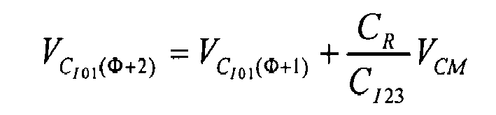


![]()
![]()
![]()
![]()


Da die Integrationskapazitäten CI01 und CI23 zumindest annähernd gleich gross sind (CI01 = CI01 = CI01), ist die Spannung VOUT(n) zwischen den Ausgängen des Operationsverstärkers 7 nach dem n-ten 4-Phasen-Zyklus 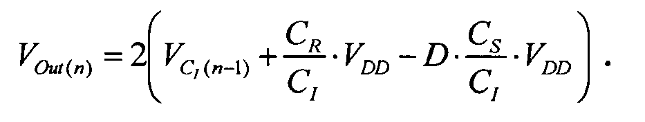
Die Spannungsänderung ΔVOUT am Ausgang des Operationsverstärkers 7 nach einem 4-Phasen-Zyklus ist somit im Falle von D = 0 proportional zum Verhältnis aus Referenzkapazität CR und Integrationskapazität CI und im Falle von D = 1 proportional zum Verhältnis aus der Differenz zwischen Referenzkapazität CR und Messkapazität CS und der Integrationskapazität CI: 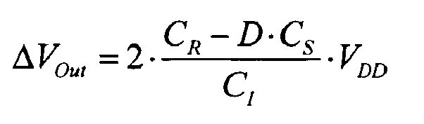
Parasitärkapazitäten und Common-Mode-Spannungen des Operationsverstärkers 7 haben keinen Einfluss auf die Ausgangsspannungen des Operationsverstärkers 7. Die vom Bitstream am Ausgang der Triggervorrichtung 15 erzeugbare mittlere Ausgangsspannung beträgt 
und ist somit umgekehrt proportional zur Messkapazität CS.Parasitic capacitances and common-mode voltages of the
and is thus inversely proportional to the measurement capacity C S.
Die
- K1: Ausgangszustand D (L oder H) der Triggervorrichtung 15,
- K2: Spannung am invertierenden Eingang des
Operationsverstärkers 7, - K3: Spannung am nicht-invertierenden Eingang des
Operationsverstärkers 7 - K4: Differentielle Integratorausgangsspannung
- K1: initial state D (L or H) of the
trigger device 15, - K2: voltage at the inverting input of the
operational amplifier 7, - K3: voltage at the non-inverting input of the
operational amplifier 7 - K4: Differential integrator output voltage
Die Zeitskala (2µs/Einheit) ist bei allen Kurven K1 bis K4 dieselbe. Die Spannungsskalen bei den Kurven K2, K3 und K4 sind in V/Einheit oder mV/Einheit angegeben. Die Werte der Messkapazität CS betragen 1.12pF bei
Das Ausgangssignal (D) der Triggervorrichtung 15 besteht aus Rechtecksignalen, die während jeweils vier Systemtakten (Clock) bzw. während eines 4-Phasen-Zyklus das Potential VH aufweisen und in einem zeitlichen Abstand aufeinander folgen, der umgekehrt proportional zur Messkapazität CS ist. Dieses Signal kann z.B. bei einem kapazitiven Distanzsensor als pulsbreiten-moduliertes Abstandsignal ausgegeben werden. Alternativ kann das Signal auch digital weiter verarbeitet werden, wobei die zeitlichen Abstände aufeinander folgender Pulse ausgewertet werden. Die Übertragungsfunktion bzw. die Kennlinie des Sensors kann dabei individuell vorgegeben werden. Bei einer weiteren alternativen Ausgestaltung des kapazitiven Sensors kann aus dem Ausgangssignal der Triggervorrichtung 15 z.B. durch ein nachgeschaltetes Filter auf einfache Weise ein analoges Ausgangssignal erzeugt werden, welches eine -zumindest näherungsweise - linearisierte Funktion eines vom Sensor zu erfassenden Objektabstandes oder des Kehrwertes der Messkapazität CS darstellt.
Die Werte der Integrationskapazitäten CI01 und CI23 und der Referenzkapazität CR können je nach gewünschtem Messbereich und/oder erforderlicher Auflösung oder Genauigkeit des Sensors festgelegt werden. Insbesondere kann vorgesehen sein, dass der Wert jeder der Integrationskapazitäten CI01 und CI23 z.B. durch die Steuerelektronik veränderbar ist, indem jeweils zwei oder mehrere Kondensatoren durch elektronische Schalter parallel geschaltet werden und gemeinsam die Integrationskapazität CI01 bzw. CI23 bilden. In analoger Weise kann auch der Wert der extern an den Chip angeschlossenen Referenzkapazität CR verändert und an die jeweiligen Erfordernisse angepasst werden. Selbstverständlich können nebst kapazitiven analogen Distanzsensoren auch Näherungsschalter oder beliebige andere Sensoren, bei denen eine Kapazität erfasst werden muss, in der erfindungsgemässen Weise ausgebildet werden. Dadurch, dass die elektronische Schaltung mit dem Delta-Sigma-Wandler monolithisch bzw. auf nur einem Chip integriert ist, kann sichergestellt werden, dass die beiden Integrationskapazitäten CI01 und CI23 und die Parasitärkapazitäten CPR und CPR' bzw. CPS und CPS' der Eingänge nahezu identisch sind.The time scale (2μs / unit) is the same for all curves K1 to K4. The voltage scales at curves K2, K3 and K4 are given in V / unit or mV / unit. The values of the measuring capacity CS are 1.12pF at
The output signal (D) of the triggering
The values of the integration capacitances C I01 and C I23 and the reference capacitance C R can be determined depending on the desired measuring range and / or the required resolution or accuracy of the sensor. In particular, it can be provided that the value of each of the integration capacitances C I01 and C I23 can be varied, for example, by the control electronics, in that two or more capacitors are connected in parallel by electronic switches and together Integrating capacity C I01 or C I23 form. In an analogous manner, the value of the externally connected to the chip reference capacitance C R can be changed and adapted to the respective requirements. Of course, in addition to capacitive analog distance sensors, it is also possible to design proximity switches or any other sensors in which a capacitance must be detected in the manner according to the invention. Due to the fact that the electronic circuit with the delta-sigma converter is monolithically or integrated on only one chip, it can be ensured that the two integration capacities C I01 and C I23 and the parasitic capacitances CPR and CPR 'or CPS and CPS' of the Inputs are almost identical.
Herkömmliche kapazitive Distanzsensoren messen die Kapazität zwischen der Sensorelektrode und dem Target (d.h. dem Objekt, dessen Abstand zum Sensor gemessen werden soll). Weil sich die gemessene Kapazität umgekehrt proportional zum Abstand zwischen Sensorelektrode und Target verhält, sinkt die Messempfindlichkeit bzw. der Quotient "relative Ausgangsgrössenänderung dividiert durch zugehörige relative Wegänderung" mit zunehmender Distanz. Die Messgenauigkeit wird somit bei derartigen herkömmlichen Sensoren mit zunehmender Distanz schlechter. Dies gilt auch bei bekannten kapazitiven Sigma-Delta-Sensoren.Conventional capacitive distance sensors measure the capacitance between the sensor electrode and the target (ie, the object whose distance to the sensor is to be measured). Because the measured capacitance behaves inversely proportional to the distance between the sensor electrode and the target, the measurement sensitivity or the quotient "relative output variable change divided by relative displacement change" decreases with increasing distance. The measurement accuracy is thus worse in such conventional sensors with increasing distance. This also applies to known capacitive sigma-delta sensors.
Mit dem neuen Verfahren wird dieses Problem dadurch gelöst, dass nicht die Kapazität C, sondern eine dazu reziproke Grösse 1/C gemessen wird. Dadurch verhält sich die Ausgangsgrösse des Sensors zumindest näherungsweise proportional zur Distanz des Targets, und die Empfindlichkeit und Genauigkeit des Sensors bleiben bis zu grösseren Distanzen erhalten. Beim erfindungsgemässen Sensor ist der Messbereich nicht primär durch die mit zunehmender Distanz abnehmende Empfindlichkeit (Änderung der Ausgangsgrösse pro Millimeter Distanzänderung), sondern durch den Signal-zu-Rauschabstand limitiert, der sich mit grösser werdendem Abstand verschlechtert. Da in der Praxis keine idealen Plattenkondensatoren verwendet werden, können Feldverzerrungen am Rand der Elektroden leichte Abweichungen der Ausgangskennlinie bewirken, welche die Abhängigkeit der Messgrösse 1/C von der Targetdistanz angibt. Diese Abweichungen sind jedoch im Vergleich zum Genauigkeitsgewinn von untergeordneter Bedeutung. Im Weiteren wird darauf hingewiesen, dass die Impulsdichte des Ausgangssignals (d.h. die Anzahl der Impulse pro Zeiteinheit) mit zunehmendem Abstand steigt, was bei grösseren Distanzen eine grössere Messbandbreite und somit eine kürzere Reaktionszeit des Sensors bewirken kann.With the new method, this problem is solved by not measuring the capacitance C, but a
Claims (10)
dadurch gekennzeichnet,
dass der Operationsverstärker (7) einen volldifferentiellen Aufbau aufweist, wobei in einem Rückkopplungszweig zwischen dem negativen Ausgang und dem nicht-invertierenden Eingang des Operationsverstärkers (7) ein Integrationskondensator mit einer ersten Integrationskapazität CI01 und in einem Rückkopplungszweig zwischen dem positiven Ausgang und dem invertierenden Eingang des Operationsverstärkers (7) ein Integrationskondensator mit einer zweiten Integrationskapazität CI23 angeordnet sind,
dass der Messkondensator (1) und der Referenzkondensator (3) je mit einer ersten Elektrode mit einem vorgegebenen Bezugsspannungspotential verbunden sind, und dass die jeweils anderen bzw. zweiten Elektroden des Messkondensators (1) und des Referenzkondensators (3) über eine Schaltelemente bzw. Schalter (5) umfassende Schaltvorrichtung mit dem nicht-invertierenden und mit dem invertierenden Eingang des Operationsverstärkers (7) verbindbar sind.Capacitive sensor comprising a measuring capacitor (1) having a measuring capacitance C S which can be influenced by external factors, a reference capacitor (3) having a reference capacitance C R , an operational amplifier (7) and a triggering device (15) connected to the output side of the operational amplifier (7). .
characterized,
that the operational amplifier (7) has a fully differential construction, wherein in a feedback branch between the negative output and the non-inverting input of the operational amplifier (7) an integration capacitor having a first integration capacitance C I01 and in a feedback branch between the positive output and the inverting input the operational amplifier (7) an integration capacitor having a second integration capacity C I23 are arranged,
that the measuring capacitor (1) and the reference capacitor (3) are each connected to a first electrode with a predetermined reference voltage potential, and that the respective other or second electrode of the measuring capacitor (1) and of the reference capacitor (3) via a switching element or switch (5) comprehensive switching device with the non-inverting and connectable to the inverting input of the operational amplifier (7).
Applications Claiming Priority (1)
| Application Number | Priority Date | Filing Date | Title |
|---|---|---|---|
| CH00203/09A CH700376A2 (en) | 2009-02-11 | 2009-02-11 | Capacitive sensor and method for capacitive sensing an object distance. |
Publications (2)
| Publication Number | Publication Date |
|---|---|
| EP2233890A2 true EP2233890A2 (en) | 2010-09-29 |
| EP2233890A3 EP2233890A3 (en) | 2014-12-24 |
Family
ID=42460475
Family Applications (1)
| Application Number | Title | Priority Date | Filing Date |
|---|---|---|---|
| EP10405024.0A Withdrawn EP2233890A3 (en) | 2009-02-11 | 2010-02-10 | Capacitive sensor and method for capacitive recording the distance of an object |
Country Status (2)
| Country | Link |
|---|---|
| EP (1) | EP2233890A3 (en) |
| CH (1) | CH700376A2 (en) |
Cited By (2)
| Publication number | Priority date | Publication date | Assignee | Title |
|---|---|---|---|---|
| EP3415872A1 (en) * | 2017-05-19 | 2018-12-19 | Simmonds Precision Products, Inc. | High accuracy, low power signal conditioner |
| CN114915290A (en) * | 2022-04-25 | 2022-08-16 | 西安航天民芯科技有限公司 | Parasitic capacitance balancing circuit and method for unipolar plate capacitance direct conversion sensor |
Families Citing this family (3)
| Publication number | Priority date | Publication date | Assignee | Title |
|---|---|---|---|---|
| DE102013201704A1 (en) * | 2013-02-01 | 2014-08-07 | Di-Soric Gmbh & Co. Kg | Capacitive sensor arrangement and capacitive measuring method with compensation of parasitic capacitances |
| EP3663779B1 (en) * | 2018-12-05 | 2021-10-06 | Nxp B.V. | Apparatus and method for measuring a capacitance, and a fingerprint sensor utilizing the same |
| CN112484810A (en) * | 2020-12-02 | 2021-03-12 | 上海钛米机器人股份有限公司 | Solution detection device and method |
Citations (2)
| Publication number | Priority date | Publication date | Assignee | Title |
|---|---|---|---|---|
| WO2006125639A1 (en) | 2005-05-25 | 2006-11-30 | Fraunhofer-Gesellschaft zur Förderung der angewandten Forschung e.V. | Capacity measuring circuit |
| WO2006132960A1 (en) | 2005-06-03 | 2006-12-14 | Synaptics Incorporated | Methods and systems for detecting a capacitance using sigma-delta measurement techniques |
Family Cites Families (5)
| Publication number | Priority date | Publication date | Assignee | Title |
|---|---|---|---|---|
| ITTO20010699A1 (en) * | 2001-07-17 | 2003-01-17 | St Microelectronics Srl | METHOD AND CIRCUIT FOR DETECTION OF MOVEMENTS THROUGH MICRO-ELECTRO-MECHANICAL SENSORS WITH COMPENSATION OF PARASITE CAPACITY AND MOVEMENT |
| WO2006098976A2 (en) * | 2005-03-09 | 2006-09-21 | Analog Devices, Inc | One terminal capacitor interface circuit |
| DE102005028507B3 (en) * | 2005-06-17 | 2006-11-30 | Texas Instruments Deutschland Gmbh | Method for capacitance-voltage conversion and capacitance-voltage converter |
| EP1790988B1 (en) * | 2005-11-29 | 2017-01-18 | STMicroelectronics Srl | Detection circuit using a differential capacitive sensor with input-common-mode control in a sense interface |
| EP1811309B1 (en) * | 2006-01-20 | 2009-10-07 | STMicroelectronics S.r.l. | Free fall detector device and free fall detection method |
-
2009
- 2009-02-11 CH CH00203/09A patent/CH700376A2/en not_active Application Discontinuation
-
2010
- 2010-02-10 EP EP10405024.0A patent/EP2233890A3/en not_active Withdrawn
Patent Citations (2)
| Publication number | Priority date | Publication date | Assignee | Title |
|---|---|---|---|---|
| WO2006125639A1 (en) | 2005-05-25 | 2006-11-30 | Fraunhofer-Gesellschaft zur Förderung der angewandten Forschung e.V. | Capacity measuring circuit |
| WO2006132960A1 (en) | 2005-06-03 | 2006-12-14 | Synaptics Incorporated | Methods and systems for detecting a capacitance using sigma-delta measurement techniques |
Cited By (3)
| Publication number | Priority date | Publication date | Assignee | Title |
|---|---|---|---|---|
| EP3415872A1 (en) * | 2017-05-19 | 2018-12-19 | Simmonds Precision Products, Inc. | High accuracy, low power signal conditioner |
| US10641620B2 (en) | 2017-05-19 | 2020-05-05 | Simmonds Precision Products, Inc. | High accuracy, low power signal conditioner |
| CN114915290A (en) * | 2022-04-25 | 2022-08-16 | 西安航天民芯科技有限公司 | Parasitic capacitance balancing circuit and method for unipolar plate capacitance direct conversion sensor |
Also Published As
| Publication number | Publication date |
|---|---|
| EP2233890A3 (en) | 2014-12-24 |
| CH700376A2 (en) | 2010-08-13 |
Similar Documents
| Publication | Publication Date | Title |
|---|---|---|
| EP2715384B1 (en) | Method for operating a hall sensor assembly, and hall sensor assembly | |
| EP1500940B1 (en) | Method for evaluating a capacitor | |
| DE19739532C2 (en) | Capacitance sensor interface circuit | |
| DE2842028C3 (en) | Device for measuring the capacitance of a capacitor | |
| EP1419365B1 (en) | Device and method for reading out a differential capacitor comprising a first and second partial capacitor | |
| DE102006051365B4 (en) | Measuring amplification device and method | |
| DE102010039272B3 (en) | Capacitance measuring circuit, sensor system and method for measuring a capacitance using a sinusoidal voltage signal | |
| EP0503272B1 (en) | Circuit arrangement for measuring the capacitance ratio of two capacitors | |
| WO2015185401A1 (en) | Method and device for monitoring the filling level of a medium in a container | |
| WO2011063536A1 (en) | Digital charge amplifier and method for converting charge signals into digital signals | |
| EP0445267B1 (en) | Device for processing sensor signals | |
| CH665027A5 (en) | METHOD FOR MEASURING AND DIGITIZING A RESISTANCE AND CIRCUIT FOR CARRYING OUT THE METHOD. | |
| EP2233890A2 (en) | Capacitive sensor and method for capacitive recording the distance of an object | |
| EP0458931B1 (en) | Arrangement for processing sensor signals | |
| DE102014216998B4 (en) | Capacitive sensor, the associated evaluation circuit and actuator in a motor vehicle | |
| DE10204652B4 (en) | Circuit arrangement, electrochemical sensor, sensor arrangement and method for processing a current signal provided via a sensor electrode | |
| DE2923026C2 (en) | Process for analog / digital conversion and arrangement for carrying out the process | |
| DE102018118646B3 (en) | Method for monitoring the function of a pressure measuring cell of a capacitive pressure sensor | |
| DE102019129264A1 (en) | Method for monitoring the function of a capacitive pressure measuring cell | |
| DE4237196C1 (en) | Method and arrangement for measuring at least one capacitance | |
| EP0847138A2 (en) | Capacitive sensing device | |
| DE3940537A1 (en) | ARRANGEMENT FOR PROCESSING SENSOR SIGNALS | |
| EP1145015B1 (en) | Acceleration measuring device | |
| EP0753756A2 (en) | Circuit and process for measuring the difference between the capacity of two capacitors | |
| DE102007025947B4 (en) | Integrated capacitive sensor |
Legal Events
| Date | Code | Title | Description |
|---|---|---|---|
| PUAI | Public reference made under article 153(3) epc to a published international application that has entered the european phase |
Free format text: ORIGINAL CODE: 0009012 |
|
| AK | Designated contracting states |
Kind code of ref document: A2 Designated state(s): AT BE BG CH CY CZ DE DK EE ES FI FR GB GR HR HU IE IS IT LI LT LU LV MC MK MT NL NO PL PT RO SE SI SK SM TR |
|
| AX | Request for extension of the european patent |
Extension state: AL BA RS |
|
| PUAL | Search report despatched |
Free format text: ORIGINAL CODE: 0009013 |
|
| AK | Designated contracting states |
Kind code of ref document: A3 Designated state(s): AT BE BG CH CY CZ DE DK EE ES FI FR GB GR HR HU IE IS IT LI LT LU LV MC MK MT NL NO PL PT RO SE SI SK SM TR |
|
| AX | Request for extension of the european patent |
Extension state: AL BA RS |
|
| RIC1 | Information provided on ipc code assigned before grant |
Ipc: G01D 5/24 20060101AFI20141118BHEP |
|
| STAA | Information on the status of an ep patent application or granted ep patent |
Free format text: STATUS: THE APPLICATION IS DEEMED TO BE WITHDRAWN |
|
| 18D | Application deemed to be withdrawn |
Effective date: 20150625 |