EP2713495A2 - Système de convertisseur multiniveaux - Google Patents
Système de convertisseur multiniveaux Download PDFInfo
- Publication number
- EP2713495A2 EP2713495A2 EP13184041.5A EP13184041A EP2713495A2 EP 2713495 A2 EP2713495 A2 EP 2713495A2 EP 13184041 A EP13184041 A EP 13184041A EP 2713495 A2 EP2713495 A2 EP 2713495A2
- Authority
- EP
- European Patent Office
- Prior art keywords
- string
- bus
- power converter
- semiconductor switches
- controllable semiconductor
- Prior art date
- Legal status (The legal status is an assumption and is not a legal conclusion. Google has not performed a legal analysis and makes no representation as to the accuracy of the status listed.)
- Granted
Links
Images


Classifications
-
- H—ELECTRICITY
- H02—GENERATION; CONVERSION OR DISTRIBUTION OF ELECTRIC POWER
- H02M—APPARATUS FOR CONVERSION BETWEEN AC AND AC, BETWEEN AC AND DC, OR BETWEEN DC AND DC, AND FOR USE WITH MAINS OR SIMILAR POWER SUPPLY SYSTEMS; CONVERSION OF DC OR AC INPUT POWER INTO SURGE OUTPUT POWER; CONTROL OR REGULATION THEREOF
- H02M7/00—Conversion of ac power input into dc power output; Conversion of dc power input into ac power output
- H02M7/42—Conversion of dc power input into ac power output without possibility of reversal
- H02M7/44—Conversion of dc power input into ac power output without possibility of reversal by static converters
- H02M7/48—Conversion of dc power input into ac power output without possibility of reversal by static converters using discharge tubes with control electrode or semiconductor devices with control electrode
- H02M7/505—Conversion of dc power input into ac power output without possibility of reversal by static converters using discharge tubes with control electrode or semiconductor devices with control electrode using devices of a thyratron or thyristor type requiring extinguishing means
- H02M7/515—Conversion of dc power input into ac power output without possibility of reversal by static converters using discharge tubes with control electrode or semiconductor devices with control electrode using devices of a thyratron or thyristor type requiring extinguishing means using semiconductor devices only
- H02M7/5152—Conversion of dc power input into ac power output without possibility of reversal by static converters using discharge tubes with control electrode or semiconductor devices with control electrode using devices of a thyratron or thyristor type requiring extinguishing means using semiconductor devices only with separate extinguishing means
-
- H—ELECTRICITY
- H02—GENERATION; CONVERSION OR DISTRIBUTION OF ELECTRIC POWER
- H02M—APPARATUS FOR CONVERSION BETWEEN AC AND AC, BETWEEN AC AND DC, OR BETWEEN DC AND DC, AND FOR USE WITH MAINS OR SIMILAR POWER SUPPLY SYSTEMS; CONVERSION OF DC OR AC INPUT POWER INTO SURGE OUTPUT POWER; CONTROL OR REGULATION THEREOF
- H02M7/00—Conversion of ac power input into dc power output; Conversion of dc power input into ac power output
- H02M7/42—Conversion of dc power input into ac power output without possibility of reversal
- H02M7/44—Conversion of dc power input into ac power output without possibility of reversal by static converters
- H02M7/48—Conversion of dc power input into ac power output without possibility of reversal by static converters using discharge tubes with control electrode or semiconductor devices with control electrode
- H02M7/483—Converters with outputs that each can have more than two voltages levels
- H02M7/4835—Converters with outputs that each can have more than two voltages levels comprising two or more cells, each including a switchable capacitor, the capacitors having a nominal charge voltage which corresponds to a given fraction of the input voltage, and the capacitors being selectively connected in series to determine the instantaneous output voltage
-
- H—ELECTRICITY
- H02—GENERATION; CONVERSION OR DISTRIBUTION OF ELECTRIC POWER
- H02M—APPARATUS FOR CONVERSION BETWEEN AC AND AC, BETWEEN AC AND DC, OR BETWEEN DC AND DC, AND FOR USE WITH MAINS OR SIMILAR POWER SUPPLY SYSTEMS; CONVERSION OF DC OR AC INPUT POWER INTO SURGE OUTPUT POWER; CONTROL OR REGULATION THEREOF
- H02M7/00—Conversion of ac power input into dc power output; Conversion of dc power input into ac power output
- H02M7/42—Conversion of dc power input into ac power output without possibility of reversal
- H02M7/44—Conversion of dc power input into ac power output without possibility of reversal by static converters
- H02M7/48—Conversion of dc power input into ac power output without possibility of reversal by static converters using discharge tubes with control electrode or semiconductor devices with control electrode
- H02M7/483—Converters with outputs that each can have more than two voltages levels
- H02M7/487—Neutral point clamped inverters
-
- H—ELECTRICITY
- H02—GENERATION; CONVERSION OR DISTRIBUTION OF ELECTRIC POWER
- H02M—APPARATUS FOR CONVERSION BETWEEN AC AND AC, BETWEEN AC AND DC, OR BETWEEN DC AND DC, AND FOR USE WITH MAINS OR SIMILAR POWER SUPPLY SYSTEMS; CONVERSION OF DC OR AC INPUT POWER INTO SURGE OUTPUT POWER; CONTROL OR REGULATION THEREOF
- H02M1/00—Details of apparatus for conversion
- H02M1/0095—Hybrid converter topologies, e.g. NPC mixed with flying capacitor, thyristor converter mixed with MMC or charge pump mixed with buck
-
- H—ELECTRICITY
- H02—GENERATION; CONVERSION OR DISTRIBUTION OF ELECTRIC POWER
- H02M—APPARATUS FOR CONVERSION BETWEEN AC AND AC, BETWEEN AC AND DC, OR BETWEEN DC AND DC, AND FOR USE WITH MAINS OR SIMILAR POWER SUPPLY SYSTEMS; CONVERSION OF DC OR AC INPUT POWER INTO SURGE OUTPUT POWER; CONTROL OR REGULATION THEREOF
- H02M3/00—Conversion of dc power input into dc power output
- H02M3/22—Conversion of dc power input into dc power output with intermediate conversion into ac
- H02M3/24—Conversion of dc power input into dc power output with intermediate conversion into ac by static converters
- H02M3/28—Conversion of dc power input into dc power output with intermediate conversion into ac by static converters using discharge tubes with control electrode or semiconductor devices with control electrode to produce the intermediate ac
- H02M3/325—Conversion of dc power input into dc power output with intermediate conversion into ac by static converters using discharge tubes with control electrode or semiconductor devices with control electrode to produce the intermediate ac using devices of a triode or a transistor type requiring continuous application of a control signal
- H02M3/335—Conversion of dc power input into dc power output with intermediate conversion into ac by static converters using discharge tubes with control electrode or semiconductor devices with control electrode to produce the intermediate ac using devices of a triode or a transistor type requiring continuous application of a control signal using semiconductor devices only
- H02M3/337—Conversion of dc power input into dc power output with intermediate conversion into ac by static converters using discharge tubes with control electrode or semiconductor devices with control electrode to produce the intermediate ac using devices of a triode or a transistor type requiring continuous application of a control signal using semiconductor devices only in push-pull configuration
- H02M3/3376—Conversion of dc power input into dc power output with intermediate conversion into ac by static converters using discharge tubes with control electrode or semiconductor devices with control electrode to produce the intermediate ac using devices of a triode or a transistor type requiring continuous application of a control signal using semiconductor devices only in push-pull configuration with automatic control of output voltage or current
-
- H—ELECTRICITY
- H02—GENERATION; CONVERSION OR DISTRIBUTION OF ELECTRIC POWER
- H02M—APPARATUS FOR CONVERSION BETWEEN AC AND AC, BETWEEN AC AND DC, OR BETWEEN DC AND DC, AND FOR USE WITH MAINS OR SIMILAR POWER SUPPLY SYSTEMS; CONVERSION OF DC OR AC INPUT POWER INTO SURGE OUTPUT POWER; CONTROL OR REGULATION THEREOF
- H02M7/00—Conversion of ac power input into dc power output; Conversion of dc power input into ac power output
- H02M7/42—Conversion of dc power input into ac power output without possibility of reversal
- H02M7/44—Conversion of dc power input into ac power output without possibility of reversal by static converters
- H02M7/48—Conversion of dc power input into ac power output without possibility of reversal by static converters using discharge tubes with control electrode or semiconductor devices with control electrode
- H02M7/53—Conversion of dc power input into ac power output without possibility of reversal by static converters using discharge tubes with control electrode or semiconductor devices with control electrode using devices of a triode or transistor type requiring continuous application of a control signal
- H02M7/537—Conversion of dc power input into ac power output without possibility of reversal by static converters using discharge tubes with control electrode or semiconductor devices with control electrode using devices of a triode or transistor type requiring continuous application of a control signal using semiconductor devices only, e.g. single switched pulse inverters
- H02M7/5387—Conversion of dc power input into ac power output without possibility of reversal by static converters using discharge tubes with control electrode or semiconductor devices with control electrode using devices of a triode or transistor type requiring continuous application of a control signal using semiconductor devices only, e.g. single switched pulse inverters in a bridge configuration
- H02M7/53871—Conversion of dc power input into ac power output without possibility of reversal by static converters using discharge tubes with control electrode or semiconductor devices with control electrode using devices of a triode or transistor type requiring continuous application of a control signal using semiconductor devices only, e.g. single switched pulse inverters in a bridge configuration with automatic control of output voltage or current
-
- H—ELECTRICITY
- H02—GENERATION; CONVERSION OR DISTRIBUTION OF ELECTRIC POWER
- H02M—APPARATUS FOR CONVERSION BETWEEN AC AND AC, BETWEEN AC AND DC, OR BETWEEN DC AND DC, AND FOR USE WITH MAINS OR SIMILAR POWER SUPPLY SYSTEMS; CONVERSION OF DC OR AC INPUT POWER INTO SURGE OUTPUT POWER; CONTROL OR REGULATION THEREOF
- H02M7/00—Conversion of ac power input into dc power output; Conversion of dc power input into ac power output
- H02M7/66—Conversion of ac power input into dc power output; Conversion of dc power input into ac power output with possibility of reversal
- H02M7/68—Conversion of ac power input into dc power output; Conversion of dc power input into ac power output with possibility of reversal by static converters
- H02M7/72—Conversion of ac power input into dc power output; Conversion of dc power input into ac power output with possibility of reversal by static converters using discharge tubes with control electrode or semiconductor devices with control electrode
- H02M7/75—Conversion of ac power input into dc power output; Conversion of dc power input into ac power output with possibility of reversal by static converters using discharge tubes with control electrode or semiconductor devices with control electrode using devices of a thyratron or thyristor type requiring extinguishing means
- H02M7/757—Conversion of ac power input into dc power output; Conversion of dc power input into ac power output with possibility of reversal by static converters using discharge tubes with control electrode or semiconductor devices with control electrode using devices of a thyratron or thyristor type requiring extinguishing means using semiconductor devices only
- H02M7/7575—Conversion of ac power input into dc power output; Conversion of dc power input into ac power output with possibility of reversal by static converters using discharge tubes with control electrode or semiconductor devices with control electrode using devices of a thyratron or thyristor type requiring extinguishing means using semiconductor devices only for high voltage direct transmission link
-
- Y—GENERAL TAGGING OF NEW TECHNOLOGICAL DEVELOPMENTS; GENERAL TAGGING OF CROSS-SECTIONAL TECHNOLOGIES SPANNING OVER SEVERAL SECTIONS OF THE IPC; TECHNICAL SUBJECTS COVERED BY FORMER USPC CROSS-REFERENCE ART COLLECTIONS [XRACs] AND DIGESTS
- Y02—TECHNOLOGIES OR APPLICATIONS FOR MITIGATION OR ADAPTATION AGAINST CLIMATE CHANGE
- Y02E—REDUCTION OF GREENHOUSE GAS [GHG] EMISSIONS, RELATED TO ENERGY GENERATION, TRANSMISSION OR DISTRIBUTION
- Y02E60/00—Enabling technologies; Technologies with a potential or indirect contribution to GHG emissions mitigation
- Y02E60/60—Arrangements for transfer of electric power between AC networks or generators via a high voltage DC link [HVCD]
Definitions
- the invention relates generally to power converters and more specifically to a multilevel converter.
- Multilevel converters offer several advantages over an ordinary two-level converter. For example, the power quality of the multilevel converter is better than that of two level converters. Also, the multilevel converters are ideal for interface between a grid and renewable energy sources such as photovoltaics (PV), fuel cells, wind turbines, and the like. In addition, the efficiency of the multilevel converter is relatively higher as a result of its minimum switching frequency.
- PV photovoltaics
- the multilevel converters having a modular structure and without transformers have been designed.
- the modular structure of the converters allows stacking of these converters to an almost unlimited number of levels.
- the modular structure aids in scaling up to different power and voltage levels.
- certain currently available multilevel converters such as modular multilevel converters (MMC) typically employ a large number of fully controllable semiconductor switches, such as insulated gate bipolar transistors (IGBTs).
- IGBTs insulated gate bipolar transistors
- a power converter in accordance with aspects of the present disclosure, includes at least one leg.
- the at least one leg includes a first string including a plurality of controllable semiconductor switches, a first connecting node, and a second connecting node, where the first string is operatively coupled across a first bus and a second bus.
- the at least one leg includes a second string operatively coupled to the first string via the first connecting node and the second connecting node, where the second string includes a plurality of switching units.
- a method for power conversion includes coupling a first string to a second string to form a power converter, where the first string includes a plurality of controllable semiconductor switches and the second string includes a plurality of switching units. Also, the method includes generating a switching pattern for the plurality of controllable semiconductor switches and the plurality of switching units based on a first line parameter input at a first terminal of the power converter. Furthermore, the method includes selectively switching the plurality of controllable semiconductor switches and the plurality of switching units based on the generated switching pattern. The method also includes generating a second line parameter at a second terminal of the power converter based on the selective switching of the plurality of controllable semiconductor switches and the plurality of switching units.
- a system for power conversion includes a power source, a load, and a first power converter.
- the first power converter includes one or more legs, where each of the one or more legs includes a first string, where the first string includes a plurality of controllable semiconductor switches, a first connecting node, a second connecting node, and a third connecting node, and where the first string is operatively coupled across a first bus and a second bus.
- each of the one or more legs includes a second string operatively coupled to the first string via the first connecting node and the second connecting node, where the second string includes a plurality of switching units.
- the system includes a controller configured to control switching of the plurality of controllable semiconductor switches and the plurality of switching units.
- a system for power conversion includes a power source, a load, and a first power converter.
- the first power converter includes one or more legs, where each of the one or more legs includes a first string operatively coupled between a first bus and a second bus, where the first string includes a plurality of controllable semiconductor switches, a first connecting node, a second connecting node, and a third connecting node, and where the third connecting nodes of the one or more legs are operatively coupled to each other.
- each of the one or more legs includes a second string operatively coupled to the first string via the first connecting node and the second connecting node, where the second string includes a plurality of switching units.
- the system includes a controller configured to control switching of the plurality of controllable semiconductor switches and a plurality of switching units.
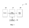
- FIG. 1 is a diagrammatical representation of a system for power conversion
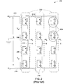
- FIG. 2 is a diagrammatical representation of a conventional modular multilevel converter
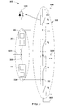
- FIG. 3 is a diagrammatical representation of an exemplary embodiment of a portion of a power converter for use in the system of FIG. 1 , according to aspects of the present disclosure
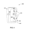
- FIG. 4 is a diagrammatical representation of an exemplary embodiment of a switching unit for use in the portion of the power converter of FIG. 3 , according to aspects of the present disclosure
- FIGs. 5(a)-5(c) are diagrammatical representations of an exemplary switching pattern of controllable semiconductor switches in the power converter of FIG. 3 , according to aspects of the present disclosure
- FIG. 6 is a diagrammatical representation of an exemplary embodiment of a three phase power converter for use in the system of FIG. 1 , according to aspects of the present disclosure
- FIG. 7 is a diagrammatical representation of an exemplary embodiment of a three phase back to back power converter for use in the system of FIG. 1 , according to aspects of the present disclosure
- FIG. 8 is a flow chart representing an exemplary method for power conversion, according to aspects of the present disclosure.
- FIG. 9 is a diagrammatical representation of voltage waveforms corresponding to different states of three phases in one line cycle, for use in the system of FIGs. 6 and 7 .
- circuit and circuitry and controller may include either a single component or a plurality of components, which are either active and/or passive and are connected or otherwise coupled together to provide the described function.
- the power converter may include a modular multilevel embedded converter.
- the term multilevel converter is used to refer to a converter that converts one form of input voltage/current to another form of output voltage/current with very low distortion.
- the system 100 for converting power may include a source 102, a power converter 104, and a grid/utility/load 106.
- the term source as used herein, is used to refer to a renewable power source, a non-renewable power source, a generator, a grid, and the like.
- the term load as used herein, may be used to refer to a grid, an electrical appliance, and the like.
- the power converter 104 may be a multilevel converter.
- the source 102 may be operatively coupled to a first terminal (not shown) of the power converter 104.
- a second terminal (not shown) of the power converter 104 may be operatively coupled to the load 106.
- the first terminal and the second terminal may be alternatively employed as an input terminal or an output terminal of the power converter 104.
- the term operatively coupled, as used herein, may include wired coupling, wireless coupling, electrical coupling, magnetic coupling, radio communication, software based communication, and the like.
- the system 100 may include a controller 108.
- the controller 108 may be configured to control the operation of the power converter 104, in one embodiment.
- the controller 108 may be configured to control the operation of the power converter 104 by controlling switching of a plurality of semiconductor switches of the power converter 104.
- the system 100 may also include other circuit components (not shown) such as, but not limited to, a transformer, a circuit breaker, an inductor, a compensator, a capacitor, a rectifier, a reactor, a filter, and the like.
- the power converter 104 will be explained in greater detail with respect to FIGs. 6 and 7 .
- the power converter 200 is a modular multilevel converter having three branches 202. Furthermore, each branch 202 includes a first portion 206 operatively coupled to a second portion 208 via an inductor 210. The inductors 210 are operatively coupled to at least one alternating current (AC) phase (A, B, and C). Furthermore, the first portion 206 and the second portion 208 may include a plurality of switching units 204, where each switching unit includes a combination of two fully controllable semiconductor switches and an energy storage device such as a capacitor. The plurality of switching units 204 is connected in series to each other.
- first end 212 of each of the three branches 202 is operatively coupled to a first bus 214, such as a positive direct current (DC) bus.
- second end 216 of each of the three branches 202 is operatively coupled to a second bus 218, such as a negative DC bus.
- a first terminal is formed by a combination of the first bus 214 and the second bus 218 and a second terminal is formed by a combination of the AC phases A, B and C.
- the voltage at the first bus 214 is +V dc and the voltage at the second bus 218 is -V dc , with respect to a virtual ground reference point N.
- the voltage at the alternating current phases A, B, and C are represented by V a , V b , and V c , respectively.
- the branch 202 is coupled between the first bus 214 and the second bus 218. Accordingly, the branch 202 may have to handle the full DC voltage (2V dc ) appearing across the first bus 214 and the second bus 218. Also, for control of the power converter 200, the first portion 206 and the second portion 208 of the branch 202 may each have to withstand a maximum voltage of 2V dc . Hence, a required number of switching units and/or a required rating of the switching units increase. By way of example, in FIG. 2 , the rating of each of the switching units is 2V dc / N 1 , where N 1 is a number of switching units in each of the first and second portions 206, 208.
- the required number of switching units in the branch 202 also increases. This leads to a higher number of fully controllable semiconductor switches in the power converter, thereby increasing the cost and the complexity of the system. Furthermore, the increased voltage across the first bus 214 and the second bus 218 also increases the rating of the switching units 204 employed in the branch 202.
- the conventional modular multilevel converter requires an increased number of switching units, thereby resulting in increased cost and complexity.
- a power converter that circumvents the shortcomings of the conventional MMC is presented.
- FIG. 3 a diagrammatical representation 300 of an exemplary embodiment of a portion of a power converter, such as the power converter 104 of FIG. 1 , is depicted.
- a leg 300 of the power converter is depicted in the embodiment of FIG. 3 .
- the leg 300 of the power converter may include a first string 302 and a second string 304. More particularly, the first string 302 may be operatively coupled to the second string 304 to form the leg 300. Furthermore, the first string 302 may be operatively coupled between a first bus 306 and a second bus 308.
- the first bus 306 may include a positive DC bus and the second bus 308 may include a negative DC bus.
- the second string 304 may be operatively coupled to the first string 302 via a first connecting node 310 and a second connecting node 312.
- the first string 302 may include a first branch 314 operatively coupled to a second branch 316 via a third connecting node 318.
- the second string 304 may include a first portion 320 operatively coupled to a second portion 322 via an AC phase 324 and an inductor 326.
- the third connecting node 318 may be operatively coupled to a third bus 328.
- the third bus 328 may be direct current bus and more particularly, a middle or center DC bus which may be at a negative potential with respect to the first bus 306 and at a positive potential with respect to the second bus 308.
- the first string 302 may include a plurality of controllable semiconductor switches S 1 , S 2 , S 3 , and S 4 (330).
- the plurality of controllable semiconductor switches may include partially controllable semiconductor switches.
- the plurality of controllable semiconductor switches may include fully controllable semiconductor switches.
- the plurality of controllable semiconductor switches may include a combination of partially controllable semiconductor switches and fully controllable semiconductor switches.
- the first string 302 may include partially controllable semiconductor switches, fully controllable semiconductor switches, or a combination of partially controllable semiconductor switches and fully controllable semiconductor switches.
- the first branch 314 of the first string 302 may include two controllable semiconductor switches S 1 and S 2 .
- the second branch 316 of the first string 302 may include two controllable semiconductor switches S 3 and S 4 .
- the controllable semiconductor switches S 1 , S 2 , S 3 , and S 4 may include a power diode in combination with a thyristor, a silicon controlled rectifier, a gate turnoff thyristor, an IGBT, and the like.
- the first portion 320 and the second portion 322 of the second string 304 may include a plurality of switching units 334.
- the switching unit 334 may be a combination of a plurality of fully controllable semiconductor switches and an energy storage device.
- the fully controllable semiconductor switches may include an insulated gate bipolar transistor (IGBT), a metal oxide semiconductor field effect transistor (MOSFET), a field effect transistor (FET), a gate turn-off thyristor, an insulated gate commutated thyristor (IGCT), an injection enhanced gate transistor (IEGT), a silicon carbide based switch, a gallium nitride based switch, a gallium arsenide based switch, or equivalents thereof.
- IGBT insulated gate bipolar transistor
- MOSFET metal oxide semiconductor field effect transistor
- FET field effect transistor
- IGCT insulated gate commutated thyristor
- IEGT injection enhanced gate transistor
- leg 300 may be employed in a single phase power converter, a two phase power converter, a three phase power converter, and other equivalent multiphase power converters.
- the switching of the controllable semiconductor switches S 1 , S 2 , S 3 and S 4 will be explained in greater detail with reference to FIGs. 5(a)-5(c) , 8 and 9 .
- diagrammatical representation 400 of an exemplary embodiment of a switching unit such as the switching unit 334 of FIG. 3 for use in the leg 300 of FIG. 3 is depicted.
- the switching unit 400 may include fully controllable semiconductor switches 402 and 404, an energy storage device 406, a first connector 408, and a second connector 410.
- the fully controllable semiconductor switches 402, 404 may include an IGBT, a MOSFET, a FET, an IEGT, a gate turn-off thyristor, an IGCT, a silicon carbide based switch, a gallium nitride based switch, a gallium arsenide based switch, or equivalents thereof.
- each of the fully controllable semiconductor switches 402, 404 may also include a power diode 412 that may be inbuilt and antiparallel to the fully controllable semiconductor switches 402 and 404.
- the inbuilt power diodes 412 may provide a freewheeling path. These power diodes 412 may also be referred to as freewheeling diodes.
- the energy storage device 406 may include a capacitor.
- the fully controllable semiconductor switch 402 may be operatively coupled in series to the energy storage device 406 to form a first limb 414.
- the other fully controllable semiconductor switch 404 forms a second limb 416.
- the second limb 416 may be operatively coupled in parallel to the first limb 414.
- the first limb 414 and the second limb 416 may be operatively coupled between the first connector 408 and the second connector 410.
- switching units 400 in a half bridge converter configuration as including two fully controllable semiconductor switches, and one energy storage device, use of other numbers of fully controllable semiconductor switches 402, 404, and energy storage devices 406 is also contemplated. In one embodiment, some or all of the switching units may be arranged to form a full bridge converter configuration.
- the energy storage device 406 may appear across the first connector 408 and the second connector 410. Consequently, the charge across the energy storage device 406 appears as a voltage across the first connector 408 and the second connector 410.
- the fully controllable semiconductor switch 404 is activated and the fully controllable semiconductor switch 402 is deactivated, the first limb 414 is bypassed, thereby providing zero voltage across the first connector 408 and the second connector 410.
- the voltage developed across the second string 304 may be regulated.
- FIGs. 5(a)-5(c) diagrammatical representations 500 of different states of a leg of a power converter, such as the leg 300 of FIG. 3 , according to the aspects of the present disclosure, are depicted.
- the switching pattern of the controllable semiconductor switches 330 (S 1 , S 2 , S 3 , and S 4 ) in the first string 302 of FIG. 3 is depicted.
- FIG. 5(a) a diagrammatical representation of a leg 502, such as the leg 300 of FIG. 3 , in a first state of switching of the controllable semiconductor switch is presented.
- the first state may also be referred to as a positive state.
- the leg 502 may include a first string 504 and a second string 506.
- the leg 502 may be operatively coupled between a first bus 508 and a second bus 510.
- the first bus 508 may include a positive DC bus
- the second bus 510 may include a negative DC bus.
- the first string 504 may be operatively coupled to the second string 506 via a first connecting node 512 and a second connecting node 514.
- a first portion such as the first portion 320 of FIG. 3 of the second string 506 and a second portion, such as the second portion 322 of FIG. 3 of the second string 506 may be represented by voltage sources V p 516 and V n 518, respectively.
- the second string 506 may include a plurality of switching units (not shown). The first portion of the second string 506 and the second portion of the second string 506 may be operatively coupled via an alternating current phase 520.
- the first string 504 may include a third connecting node 522, which may be operatively coupled to a third bus 524.
- the first string 504 includes four controllable semiconductor switches represented as S 1 , S 2 , S 3 and S 4 .
- the voltage at the first bus 508 may be represented as +V dc and the voltage at the second bus 510 may be represented as -V dc .
- the voltage of +V dc at the first bus 508 and the voltage of -V dc at the second bus 510 may be with respect to a virtual ground.
- the voltage at the third bus 524 may be represented as V mid
- the voltage at the alternating current phase may be represented as V ac .
- controllable semiconductor switches S 1 and S 3 are activated, while the controllable semiconductor switches S 2 and S 4 are maintained in a deactivated state.
- the activation of controllable semiconductor switches S 1 and S 3 provides a first current flow path 526 between the first bus 508 and the third bus 524 via a corresponding second string 506. Consequently, the second string 506 may be operatively coupled between the first bus 508 and the third bus 524 in the positive state.
- the voltage across the first bus 508 and the third bus 524 may depend on the switching of the fully controllable semiconductor switches corresponding to the plurality of switching units in the second string 506, such as the switching units 334 of FIG. 3 .
- the current flowing through the first current flow path 526 is represented as I dc .
- FIG. 5(b) is a diagrammatical representation 528 of a leg in a second state of switching of the controllable semiconductor switches.
- the second state of switching of the controllable semiconductor switches may also be referred to as a negative state.
- FIG. 5(b) is explained with reference to FIG. 5(a) .
- the controllable semiconductor switches S 2 and S 4 may be activated, while controllable semiconductor switches S 1 and S 3 are deactivated.
- the activation of the controllable semiconductor switches S 2 and S 4 may result in providing a second current flow path 530 between the third bus 524 and the second bus 510.
- the second string 506 may be operatively coupled between the second bus 510 and the third bus 524 in the negative state.
- FIG. 5(c) is a diagrammatical representation 532 of a leg in a third state of switching of the controllable semiconductor switches.
- the third state of switching of the controllable semiconductor switches may also be referred to as a zero state.
- FIG. 5(c) is explained with reference to FIG. 5(a) .
- the controllable semiconductor switches S 2 and S 3 may be activated, while the controllable semiconductor switches S 1 , and S 4 are deactivated.
- the activation of the controllable semiconductor switches S 2 and S 3 may result in providing a third current flow path 534. Subsequently, the current flows in the third current flow path 534.
- This third current flow path 534 may also be referred to as a freewheeling path.
- both ends of the second string 506 may be operatively coupled to each other via the activated controllable semiconductor switches S 2 and S 3 and the third bus 524.
- FIGs. 5(a)-5(c) represent the three states of switching with reference to a single leg, these three states of switching may be employed simultaneously for a plurality of legs in a two phase power converter, a three phase power converter, and the like.
- the branch 202 has to withstand a voltage of 2V dc .
- the second string 506 is operatively coupled between the first bus 508 and third bus 524, between the third bus 524 and the second bus 510, or both ends of the second string 506 may be operatively coupled to a third bus 524.
- the second string 506 may have to withstand a maximum voltage of value V dc .
- the first portion of the second string 506 and the second portion of the second string 506 may each have to withstand a maximum voltage of V dc . Consequently, a desired number of switching units in the second string 506 may be reduced.
- the voltage across each of the switching units such as switching units 334 of FIG. 3 in the second string 506 may be assumed to be 1V.
- V dc is 8 volts
- the conventional power converter 200 entails use of 32 switching units in the branch 202 of FIG. 2 .
- the number of switching units in the second string 506 may at least be halved to 16. Consequently, the number of the fully controllable semiconductor switches may also be correspondingly reduced. Accordingly, the conduction and switching losses corresponding to the fully controllable semiconductor switches is also reduced by half.
- the switching of the plurality of controllable semiconductor switches S 1 , S 2 , S 3 , and S 4 of the first string 504 may operate in combination with the switching of the plurality of switching units (not shown) in the second string 506.
- the switching of the plurality of switching units in the second string 506 may include activation and/or deactivation of the fully controllable semiconductor switches.
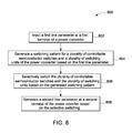
- FIG. 6 a diagrammatical representation 600 of an exemplary embodiment of a three phase multilevel converter, according to aspects of the present disclosure, is depicted.
- the power converter 600 is a three phase modular multilevel embedded converter.
- the three phase multilevel converter 600 includes three legs 626, 628, 630. Each leg may include a respective first and second string 602, 604.
- the first string 602 includes a first branch 606 and a second branch 608.
- one end of the second string 604 may be operatively coupled to a first connecting node 614 of a respective first string 602, and the other end of the second string 604 may be operatively coupled to a second connecting node 616 of the same first string 602.
- one end of a first portion 610 of the second string 604 may be operatively coupled to the first string 602 via the first connecting node 614.
- the first connecting node 614 may be situated between two controllable semiconductor switches 638 (S 1 and S 2 ) of the first branch 606 of the first string 602.
- one end of a second portion 612 of the second string 604 may be operatively coupled to the first string 602 via the second connecting node 616.
- the second connecting node 616 may be situated between two controllable semiconductor switches 638 (S 3 and S 4 ) of the second branch 608 of the first string 602.
- the first portion 610 of the second string 604 may be operatively coupled to the second portion 612 of the second string 604 via a fourth bus.
- the term fourth bus may be an alternating current (AC) phase.
- each of the three legs 626, 628, 630 may be associated with at least one AC phase.
- a three phase AC system may include an AC phase-A 632, an AC phase-B 634, and an AC phase-C 636.
- a first terminal (not shown) may be formed by a combination of a first bus 620 and a second bus 622. The first terminal may also be referred to as a DC terminal.
- the AC phases, AC phase-A 632, AC phase-B 634, and AC phase-C 636 in combination may form a second terminal (not shown).
- the second terminal may also be referred to as an AC terminal.
- two DC voltage sources 640 may be operatively coupled between the first bus 620 and the second bus 622. However, in one example, the use of other number of DC voltage sources is contemplated.
- first branch 606 may be operatively coupled to the second branch 608 via a third connecting node 618.
- the third connecting node 618 may be the middle point of the first string 602.
- the third connecting nodes 618 of each of the three first strings 602 may be operatively coupled to each other to form a floating point.
- the third connecting nodes 618 of each of the three first strings 602 may be operatively coupled to a third bus 624.
- the third bus 624 may be a middle or center DC bus.
- the third connecting nodes 618 of each of the three first strings 602 may be operatively coupled to a neutral bus.
- the three legs 626, 628, 630 may be operatively coupled between the first bus 620 and the second bus 622.
- the power converter 600 may be operatively coupled to a controller such as the controller 108 of FIG. 1 .
- the first strings 602 may include a plurality of controllable semiconductor switches
- the second strings 604 may include a plurality of switching units.
- the controller may be configured to control the switching of the plurality of controllable semiconductor switches in the first strings 602 and the plurality of switching units in the second strings 604.
- the switching of the switching units in the second strings 604 and that of the controllable semiconductor switches in the first strings 602 may be based on a modulation technique.
- the modulation technique may include pulse width modulation technique, space vector modulation, and the like.
- the controller may be configured to aid in the generation of a sinusoidal voltage at the alternating current phases 632, 634, 636 with respect to the third bus 624.
- the controller may be configured to balance and regulate energy stored in the second string 604 during a line cycle. Accordingly, the controller may be configured to ensure that an average power of a second string 604 during one line cycle is zero.
- the term line cycle as used herein, may be an AC voltage cycle.
- the controller may also be configured to regulate currents in the first string 602 and the second string 604 to maintain the voltage at the third connecting node 618 at a value that is substantially equal to the voltage at the third bus 624.
- the controller may be disposed at a remote location.
- the back to back mode three phase power converter 700 may include a first converter 702 operatively coupled to a second converter 706.
- the first converter 702 and the second converter 706 may have a topology that is substantially similar to the topology of the power converter 600 of FIG. 6 .
- the first converter 702 and the second converter 706 may each include three legs 708.
- the first converter 702 and the second converter 706 may be operatively coupled via a first bus 710 and a second bus 712.
- the first bus 710 and the second bus 712 may be replaced by a high voltage direct current (HVDC) transmission line.
- HVDC high voltage direct current
- Each of the legs 708 may include a first string 714 operatively coupled to a second string 716.
- the first string 714 such as the first string 302 of FIG. 3
- the second string 716 such as the second string 304 of FIG. 3
- the power converter 700 may be employed to facilitate transfer of power in one direction or in both directions.
- the power converter 700 may be used to connect and transfer power between two alternating current grids of different frequencies. In this example, it may be desirable to provide isolation between the two alternating current grids.
- a flow chart 800 representing an exemplary method for power conversion, according to aspects of the present disclosure, is depicted.
- the method begins at step 802, where a first line parameter may be input at a first terminal of the power converter 600.
- the first line parameter may include a DC voltage, a DC current, an AC voltage, an AC current, or equivalents thereof.
- a DC voltage may be input at the first terminal and an AC voltage may be obtained as an output at a second terminal of the power converter 600.
- the AC phases, AC phase-A 632, AC phase-B 634, and AC phase-C 636 in combination may form the second terminal of the power converter 600.
- the first terminal and the second terminal may be used alternatively as an input terminal and an output terminal.
- the DC terminal may be the input terminal and the AC terminal may be the output terminal.
- the AC terminal may be the input terminal and the DC terminal may be the output terminal.
- a switching pattern corresponding to the plurality of controllable semiconductor switches such as S 1 , S 2 , S 3 , and S 4 of FIG. 6 and the plurality of fully controllable semiconductor switches of the switching units such as the switching units 334 of FIG. 3 may be generated based on the first line parameter input at the first terminal.
- the term switching pattern may be representative of a manner in which the plurality of controllable semiconductor switches S 1 , S 2 , S 3 , and S 4 and the plurality of fully controllable semiconductor switches of the switching units may be activated and/or deactivated.
- the switching patterns corresponding to the plurality of controllable semiconductor switches S 1 , S 2 , S 3 , and S 4 and the plurality of fully controllable semiconductor switches of the switching units 334 may vary based on the first line parameter. Furthermore, in one example, the switching pattern corresponding to the plurality of controllable semiconductor switches S 1 , S 2 , S 3 , and S 4 and the plurality of fully controllable semiconductor switches of the switching units 334 may also depend on a desired output to be generated.
- the plurality of controllable semiconductor switches S 1 , S 2 , S 3 , and S 4 in the first string 602 and the plurality of switching units in the second string 604 may be selectively switched based on the switching pattern generated at step 804.
- the term switching may include activation and/or deactivation of the plurality of controllable semiconductor switches S 1 , S 2 , S 3 , and S 4 in the first string 602.
- the switching of the plurality of switching units in the second string 604 may include activation and/or deactivation of the fully controllable semiconductor switches in the switching units.
- a second line parameter may be generated at the second terminal of the power converter 600 based on selective switching of step 806.
- the second line parameter may include a DC voltage, an AC voltage and the like, in one example.
- the switching of the controllable semiconductor switches during a zero state, a positive state, and a negative state of the legs, such as the legs 626, 628, 630 of FIG. 6 aid in the generation of the second line parameter which is representative of an output of the modular multilevel embedded converter 600 of FIG. 6 .
- FIG. 9 a diagrammatical representation 900 of voltage waveforms corresponding to the different states of three AC phases (see FIG. 6 ) in one line cycle 901, according to the aspects of the present disclosure, is depicted.
- the line cycle 901 may be partitioned into six sections 902, 904, 906, 908, 910, 912.
- the three AC phases may include the AC-phase A 632, the AC phase-B 634, and the AC phase-C 636.
- voltage waveforms corresponding to the AC three phases A, B, and C are presented.
- the voltage waveforms corresponding to the three phases may include a first voltage waveform 914 corresponding to AC phase-A, a second voltage waveform 916 corresponding to AC phase-B, and a third voltage waveform 918 corresponding to AC phase-C.
- the six sections 902, 904, 906, 908, 910, and 912 may have corresponding switching patterns to generate desired outputs.
- the switching pattern may be determined at step 804 of FIG. 8 .
- the line cycle 901 of the three AC phases may include six transient zones 920, 922, 924, 926, 928, and 930.
- the term transient zone is used to refer to a zone during which at least one of the legs 626, 628, 630 transitions from one state to another. In one non-limiting example, at the transient zone 922, the state of the leg 630 associated with AC phase C changes from a positive state to a negative state.
- one of the legs may be in the positive state, while another leg may be in the negative state, and yet another leg may be in the zero state.
- the leg 626 associated with AC phase A and the leg 630 associated with AC phase C may be in the positive state, while the leg 628 associated with AC phase B may be in the negative state.
- the leg 626 associated with AC phase A and the leg 630 associated with AC phase C may be operatively coupled in parallel to each other between the first bus 620 and the third bus 624.
- the second string 604 associated with the AC phase-A and the second string 604 associated with the AC phase-C may be operatively coupled in parallel to each other between the first bus 620 and the third bus 624 through the activated switches S 1 and S 3 of the corresponding first strings 602.
- the leg 628 associated with AC phase B may be operatively coupled between the third bus 624 and the second bus 622.
- the switches S 2 and S 4 corresponding to the first string 602 associated with AC phase B may be activated.
- the leg 626 associated with AC phase A and the leg 630 associated with AC phase C may be operatively coupled in parallel to each other and further operatively coupled in series to the leg 628 associated with AC phase B, as indicated by reference numeral 932.
- the section 902 is followed by the transient zone 922.
- the leg 626 associated with AC phase A continues to be in the positive state and the leg 628 associated with AC phase B continues to be in negative state.
- the leg 630 associated with AC phase C transitions from the positive state to the zero state, as indicated by reference numeral 934.
- the switches S 2 and S 3 of the first string 602 associated with AC phase C may be activated. Consequently, when the leg 630 associated with AC phase C is in the zero state, both ends of the leg 630 may be operatively coupled to the third bus 624.
- the leg 630 associated with AC phase C Prior to the transient zone 922, the leg 630 associated with AC phase C is in a positive state in the section 902. Hence, at the transient zone 922, the switch S 1 corresponding to the first string 602 associated with AC-phase C may be deactivated and the switch S 2 corresponding to the first string 602 associated with AC-phase C may be activated. Switch S 2 may be activated by applying a gate trigger signal. Also, at section 902, as previously noted, the leg 626 associated with AC phase A and the leg 630 associated with AC phase C may be operatively coupled in parallel to each other between the first bus 620 and the third bus 624 through the corresponding activated switches S 1 and S 3 .
- the DC current on the first bus 620 is shared by the leg 626 associated with AC phase A and the leg 630 associated with AC phase C. Accordingly, the DC current on the first bus 620 is shared by the switches S 1 and S 3 of the first string 602 associated with AC phase A and the switches S 1 and S 3 of the first string 602 associated with AC phase C.
- the deactivation of switch S 1 corresponding to first string 602 associated with AC phase C may be achieved by reducing the current to a near zero value in the first string 602 associated with AC phase C. Furthermore, the reduction of the current to the near zero value in the first string 602 associated with AC phase C may be achieved by employing a controller such as the controller 108 of FIG. 1 .
- the switching of the controllable semiconductor switches in the first strings 602 corresponding to the legs 626, 628, 630 may be performed for sections 904, 906, 908, 910, and 912 and for the transient zones 924, 926, 928, 930, and 920 to obtain the desired output line parameter.
- the switching of the controllable semiconductor switches in the first strings corresponding to the AC phase-A, the AC phase-B, and the AC phase-C may be controlled by the controller.
- a processor-based system such as a general-purpose or special-purpose computer.
- different implementations of the present technique may perform some or all of the steps described herein in different orders or substantially concurrently, that is, in parallel.
- the functions may be implemented in a variety of programming languages, including but not limited to C++ or Java.
- Such code may be stored or adapted for storage on one or more tangible, machine readable media, such as on data repository chips, local or remote hard disks, optical disks (that is, CDs or DVDs), memory or other media, which may be accessed by a processor-based system to execute the stored code.
- tangible media may comprise paper or another suitable medium upon which the instructions are printed.
- the instructions may be electronically captured via optical scanning of the paper or other medium, then compiled, interpreted or otherwise processed in a suitable manner if necessary, and then stored in the data repository or memory.
- the various embodiments of the power converter and the methods of power conversion described hereinabove aid in developing multilevel power converters, thereby allowing generation of high power/voltage/current output. Furthermore, since the exemplary power converter utilizes about half number of switching units when compared to a conventional modular power converter, a system of lower cost may be provided. Also, use of thyristors in the power converter provides a less expensive system. Furthermore, use of the thyristors provides a power converter with substantially lower losses. In addition, the exemplary power converter may circumvent the need for additional capacitors in the DC link. The various embodiments of the power converter may find application in solar, wind, and other renewable power generation devices.
- the power converter may be employed in non-renewable power generation systems like thermal power plants, hydroelectric power plants, and equivalents thereof.
- the power converter may be employed as a DC-AC converter or an AC-DC converter for use in HVDC transmission and distribution systems.
Applications Claiming Priority (1)
| Application Number | Priority Date | Filing Date | Title |
|---|---|---|---|
| US13/629,882 US9559611B2 (en) | 2012-09-28 | 2012-09-28 | Multilevel power converter system and method |
Publications (3)
| Publication Number | Publication Date |
|---|---|
| EP2713495A2 true EP2713495A2 (fr) | 2014-04-02 |
| EP2713495A3 EP2713495A3 (fr) | 2014-12-24 |
| EP2713495B1 EP2713495B1 (fr) | 2017-11-15 |
Family
ID=49123782
Family Applications (1)
| Application Number | Title | Priority Date | Filing Date |
|---|---|---|---|
| EP13184041.5A Not-in-force EP2713495B1 (fr) | 2012-09-28 | 2013-09-12 | Système de convertisseur multiniveaux |
Country Status (5)
| Country | Link |
|---|---|
| US (1) | US9559611B2 (fr) |
| EP (1) | EP2713495B1 (fr) |
| CN (1) | CN103715931B (fr) |
| BR (1) | BR102013023246A2 (fr) |
| CA (1) | CA2827664A1 (fr) |
Cited By (12)
| Publication number | Priority date | Publication date | Assignee | Title |
|---|---|---|---|---|
| EP2843823A1 (fr) * | 2013-08-30 | 2015-03-04 | GE Energy Power Conversion Technology Limited | Convertisseur NPC de trois niveau avec thyristeurs et ponts en cascade comme commutateurs c.a. intérieurs et équilibrage d'énergie dans les ponts en cascade |
| EP2833537A3 (fr) * | 2013-07-31 | 2015-07-15 | GE Energy Power Conversion Technology Ltd | Système de convertisseur multiniveaux |
| EP2840699A3 (fr) * | 2013-07-29 | 2015-07-15 | GE Energy Power Conversion Technology Ltd | Système de convertisseur multiniveaux |
| EP2924867A1 (fr) * | 2014-03-28 | 2015-09-30 | General Electric Company | Convertisseur multi-niveaux |
| CN105610334A (zh) * | 2014-11-17 | 2016-05-25 | 通用电气能源能量变换技术有限公司 | 模块化嵌入式多级转换器和使用方法 |
| US9431918B2 (en) | 2012-09-28 | 2016-08-30 | General Electric Company | Grounding scheme for modular embedded multilevel converter |
| US9559611B2 (en) | 2012-09-28 | 2017-01-31 | General Electric Company | Multilevel power converter system and method |
| EP3104515A4 (fr) * | 2014-02-03 | 2017-09-20 | Kabushiki Kaisha Toshiba | Dispositif de conversion de puissance |
| EP3188356A4 (fr) * | 2014-08-25 | 2018-04-25 | Kabushiki Kaisha Toshiba | Dispositif de conversion de puissance |
| WO2018113944A1 (fr) * | 2016-12-21 | 2018-06-28 | Abb Schweiz Ag | Convertisseur de source de tension à fonctionnement amélioré |
| EP3120448B1 (fr) * | 2014-03-19 | 2020-04-29 | General Electric Company | Convertisseur npc de trois niveau avec thyristeur et ponts en cascade comme commutateurs c.a. intérieurs |
| US11424693B2 (en) | 2018-04-27 | 2022-08-23 | Toshiba Mitsubishi-Electric Industrial Systems Corporation | Three-level power conversion device, three-level power conversion device control method, and storage medium |
Families Citing this family (15)
| Publication number | Priority date | Publication date | Assignee | Title |
|---|---|---|---|---|
| CN104218808B (zh) * | 2014-07-25 | 2017-01-25 | 国家电网公司 | 基于模块化多电平变换器的输出电压正负极性反转方法 |
| US9537421B2 (en) * | 2014-08-22 | 2017-01-03 | General Electric Company | Multilevel converter |
| WO2016029824A1 (fr) * | 2014-08-25 | 2016-03-03 | 国家电网公司 | Dispositif de conversion de tension continue et son procédé de commande de bras de pont |
| CN106160463B (zh) * | 2015-04-01 | 2019-09-06 | 国家电网公司 | 一种直流电压变换装置及其桥臂控制方法 |
| US9525348B1 (en) | 2015-07-31 | 2016-12-20 | Abb Schweiz Ag | Power converter having integrated capacitor-blocked transistor cells |
| US10243370B2 (en) * | 2015-12-07 | 2019-03-26 | General Electric Company | System and method for integrating energy storage into modular power converter |
| JP6502870B2 (ja) * | 2016-02-04 | 2019-04-17 | 株式会社東芝 | 電力変換装置 |
| JP6524000B2 (ja) * | 2016-03-15 | 2019-06-05 | 株式会社東芝 | 電力変換装置 |
| CN107306083B (zh) * | 2016-04-22 | 2019-09-20 | 台达电子企业管理(上海)有限公司 | 飞跨电容的电压平衡控制装置与电压平衡控制方法 |
| CN107124099B (zh) * | 2017-03-09 | 2019-06-25 | 中山市波信太阳能科技有限公司 | 一种太阳能电压电流转换装置 |
| EP3467987B1 (fr) * | 2017-10-06 | 2023-12-20 | General Electric Technology GmbH | Plan de conversion |
| EP3522357A1 (fr) * | 2018-01-31 | 2019-08-07 | Siemens Aktiengesellschaft | Convertisseur modulaire multi-niveaux |
| SE542175C2 (en) | 2018-07-06 | 2020-03-10 | Abb Schweiz Ag | Improved modular multilevel converter |
| US11336203B2 (en) | 2018-09-07 | 2022-05-17 | Socovar S.E.C. | Multilevel electric power converter |
| WO2023230679A1 (fr) * | 2022-06-01 | 2023-12-07 | Weg Drives & Controls - Automação Ltda | Procédé de modulation destiné à faire fonctionner un mmc pour maximiser la tension de mode commun en réduisant les courants circulants, et support lisible par machine |
Family Cites Families (36)
| Publication number | Priority date | Publication date | Assignee | Title |
|---|---|---|---|---|
| US5644483A (en) * | 1995-05-22 | 1997-07-01 | Lockheed Martin Energy Systems, Inc. | Voltage balanced multilevel voltage source converter system |
| US5684688A (en) | 1996-06-24 | 1997-11-04 | Reliance Electric Industrial Company | Soft switching three-level inverter |
| SE511219C2 (sv) | 1998-01-27 | 1999-08-23 | Asea Brown Boveri | Omriktare där klampningsdioderna ersatts av en aktiv klampningskrets |
| SE517427C2 (sv) | 2000-10-11 | 2002-06-04 | Abb Ab | Förfarande, apparat, datorprogram och datorprogramprodukt för styrning av VSC-omriktare, samt en VSC-omriktare |
| DE10103031B4 (de) | 2001-01-24 | 2011-12-01 | Siemens Ag | Stromrichterschaltung mit verteilten Energiespeichern und Verfahren zur Steuerung einer derartigen Stromrichterschaltung |
| SE521243C2 (sv) | 2001-02-07 | 2003-10-14 | Abb Ab | Omriktaranordning samt förfarande för styrning av en sådan |
| SE524014C2 (sv) * | 2002-10-09 | 2004-06-15 | Abb Ab | Omriktare samt förfarande för styrning av en omriktare |
| SE0300704L (sv) | 2003-03-14 | 2004-09-15 | Abb Ab | VSC-strömriktare samt förfarande |
| US20050139259A1 (en) | 2003-12-30 | 2005-06-30 | Robert Steigerwald | Transformerless power conversion in an inverter for a photovoltaic system |
| US7219673B2 (en) | 2004-08-25 | 2007-05-22 | Curtiss-Wright Electro-Mechanical Corporation | Transformerless multi-level power converter |
| EP1750363A1 (fr) | 2005-08-03 | 2007-02-07 | Abb Research Ltd. | Convertisseur alternatif continu à plusieurs niveaux pour des applications en traction |
| EP1750361A1 (fr) | 2005-08-03 | 2007-02-07 | ABB Research Ltd | Dispositif de convertisseur à plusieurs niveaux et son utilisation |
| CA2622057C (fr) | 2005-09-09 | 2017-01-17 | Siemens Aktiengesellschaft | Dispositif de transmission d'energie electrique |
| WO2008002226A1 (fr) | 2006-06-28 | 2008-01-03 | Abb Technology Ltd. | Convertisseur ccht modulaire |
| WO2008024039A1 (fr) | 2006-08-25 | 2008-02-28 | Abb Technology Ltd | Filtre à courant continu et station de convertisseur de source de tension comprenant un tel filtre |
| US8144488B2 (en) | 2006-08-25 | 2012-03-27 | Abb Technology Ltd. | Voltage source converter station |
| JP5202528B2 (ja) * | 2006-09-06 | 2013-06-05 | シーメンス アクチエンゲゼルシヤフト | 電力変換器 |
| DE112006004197A5 (de) * | 2006-12-08 | 2009-11-12 | Siemens Aktiengesellschaft | Steuerung eines modularen Stromrichters mit verteilten Energiespeichern |
| CA2671818C (fr) | 2006-12-08 | 2015-09-29 | Siemens Aktiengesellschaft | Dispositif pour transformer un courant electrique |
| PL2100366T3 (pl) | 2006-12-08 | 2017-12-29 | Siemens Aktiengesellschaft | Wytwarzanie równowagi mocy czynnej modułów fazowych przekształtnika |
| WO2009026960A1 (fr) | 2007-08-29 | 2009-03-05 | Abb Technology Ag | Réacteur sec à haute tension pour convertisseur de source de tension |
| CN101803169B (zh) | 2007-09-05 | 2013-01-02 | Abb技术有限公司 | 用于高电压直流电力传输的电压源换流器 |
| DE102007044226A1 (de) * | 2007-09-17 | 2009-03-19 | Liebherr-Aerospace Lindenberg Gmbh | Vorrichtung zur Versorgung mehrerer elektrischer mehrphasiger Lasten |
| US20110019453A1 (en) | 2007-11-30 | 2011-01-27 | Roberto Gonzalez Senosiain | Electric circuit for converting direct current into alternating current |
| EP2107672A1 (fr) | 2008-03-31 | 2009-10-07 | SMA Solar Technology AG | Onduleur triphasé sans connexion entre le conducteur de neutre du réseau et le point milieu du circuit intermédiaire |
| WO2009149742A1 (fr) | 2008-06-09 | 2009-12-17 | Abb Technology Ag | Equipement de transmission d'énergie électrique |
| IT1393717B1 (it) | 2009-03-31 | 2012-05-08 | Meta System Spa | Dispositivo e metodo per la conversione di corrente continua in corrente alternata |
| US8582331B2 (en) | 2009-07-20 | 2013-11-12 | Vincotech Holdings S.à.r.l. | Inverter topologies usable with reactive power |
| US8228695B2 (en) | 2009-11-16 | 2012-07-24 | General Electric Company | Multilevel converter operation |
| KR101727778B1 (ko) | 2010-04-08 | 2017-04-17 | 제네럴 일렉트릭 테크놀러지 게엠베하 | 하이브리드 hvdc 컨버터 |
| US8848401B2 (en) | 2010-10-27 | 2014-09-30 | Alstom Technology Ltd. | Modular multilevel power electronic converter having selectively definable circulation path |
| CA2842498A1 (fr) | 2011-08-04 | 2013-02-07 | Abb Technology Ag | Convertisseur multiniveau sans transformateur |
| EP2568591A1 (fr) * | 2011-09-12 | 2013-03-13 | Green Power Technologies, S.L. | Convertisseurs multi-niveaux à couplage multi-niveaux (MLC2) |
| WO2013135277A1 (fr) | 2012-03-14 | 2013-09-19 | Abb Technology Ltd. | Convertisseur électrique modulaire à écrêteur |
| US9148069B2 (en) * | 2012-05-25 | 2015-09-29 | General Electric Company | High voltage high power multi-level drive structure |
| US9559611B2 (en) | 2012-09-28 | 2017-01-31 | General Electric Company | Multilevel power converter system and method |
-
2012
- 2012-09-28 US US13/629,882 patent/US9559611B2/en active Active
-
2013
- 2013-09-11 BR BRBR102013023246-7A patent/BR102013023246A2/pt not_active Application Discontinuation
- 2013-09-12 EP EP13184041.5A patent/EP2713495B1/fr not_active Not-in-force
- 2013-09-19 CA CA2827664A patent/CA2827664A1/fr not_active Abandoned
- 2013-09-27 CN CN201310447786.7A patent/CN103715931B/zh not_active Expired - Fee Related
Non-Patent Citations (1)
| Title |
|---|
| None |
Cited By (19)
| Publication number | Priority date | Publication date | Assignee | Title |
|---|---|---|---|---|
| US9559611B2 (en) | 2012-09-28 | 2017-01-31 | General Electric Company | Multilevel power converter system and method |
| US9431918B2 (en) | 2012-09-28 | 2016-08-30 | General Electric Company | Grounding scheme for modular embedded multilevel converter |
| EP2840699A3 (fr) * | 2013-07-29 | 2015-07-15 | GE Energy Power Conversion Technology Ltd | Système de convertisseur multiniveaux |
| EP2833537A3 (fr) * | 2013-07-31 | 2015-07-15 | GE Energy Power Conversion Technology Ltd | Système de convertisseur multiniveaux |
| US9252681B2 (en) | 2013-08-30 | 2016-02-02 | General Electric Company | Power converter with a first string having controllable semiconductor switches and a second string having switching modules |
| EP2843823A1 (fr) * | 2013-08-30 | 2015-03-04 | GE Energy Power Conversion Technology Limited | Convertisseur NPC de trois niveau avec thyristeurs et ponts en cascade comme commutateurs c.a. intérieurs et équilibrage d'énergie dans les ponts en cascade |
| US10075092B2 (en) | 2014-02-03 | 2018-09-11 | Kabushiki Kaisha Toshiba | Neutral point power converter with first and second chopper cell groups |
| EP3104515A4 (fr) * | 2014-02-03 | 2017-09-20 | Kabushiki Kaisha Toshiba | Dispositif de conversion de puissance |
| EP3120448B1 (fr) * | 2014-03-19 | 2020-04-29 | General Electric Company | Convertisseur npc de trois niveau avec thyristeur et ponts en cascade comme commutateurs c.a. intérieurs |
| US9515568B2 (en) | 2014-03-28 | 2016-12-06 | General Electric Company | Power converter with a first string having diodes and a second string having switching units |
| EP2924867A1 (fr) * | 2014-03-28 | 2015-09-30 | General Electric Company | Convertisseur multi-niveaux |
| EP3188356A4 (fr) * | 2014-08-25 | 2018-04-25 | Kabushiki Kaisha Toshiba | Dispositif de conversion de puissance |
| EP3046248A1 (fr) * | 2014-11-17 | 2016-07-20 | GE Energy Power Conversion Technology Ltd | Convertisseur multi-niveaux intégré modulaire et procédé d'utilisation |
| CN105610334A (zh) * | 2014-11-17 | 2016-05-25 | 通用电气能源能量变换技术有限公司 | 模块化嵌入式多级转换器和使用方法 |
| WO2018113944A1 (fr) * | 2016-12-21 | 2018-06-28 | Abb Schweiz Ag | Convertisseur de source de tension à fonctionnement amélioré |
| CN110100383A (zh) * | 2016-12-21 | 2019-08-06 | Abb瑞士股份有限公司 | 具有改进操作的电压源换流器 |
| US10530272B2 (en) | 2016-12-21 | 2020-01-07 | Abb Schweiz Ag | Voltage source converter with improved operation |
| CN110100383B (zh) * | 2016-12-21 | 2020-03-27 | Abb瑞士股份有限公司 | 具有改进操作的电压源换流器 |
| US11424693B2 (en) | 2018-04-27 | 2022-08-23 | Toshiba Mitsubishi-Electric Industrial Systems Corporation | Three-level power conversion device, three-level power conversion device control method, and storage medium |
Also Published As
| Publication number | Publication date |
|---|---|
| CA2827664A1 (fr) | 2014-03-28 |
| BR102013023246A2 (pt) | 2015-09-01 |
| US9559611B2 (en) | 2017-01-31 |
| EP2713495B1 (fr) | 2017-11-15 |
| CN103715931B (zh) | 2018-08-07 |
| EP2713495A3 (fr) | 2014-12-24 |
| CN103715931A (zh) | 2014-04-09 |
| US20140092661A1 (en) | 2014-04-03 |
Similar Documents
| Publication | Publication Date | Title |
|---|---|---|
| US9559611B2 (en) | Multilevel power converter system and method | |
| Siwakoti et al. | A novel seven-level active neutral-point-clamped converter with reduced active switching devices and DC-link voltage | |
| US9431918B2 (en) | Grounding scheme for modular embedded multilevel converter | |
| EP2747269B1 (fr) | Systèem convertisseur multi-niveaux aux condensateurs flottants et méthode de précharge des condensateurs dans un tel système | |
| US9479075B2 (en) | Multilevel converter system | |
| US9252681B2 (en) | Power converter with a first string having controllable semiconductor switches and a second string having switching modules | |
| da Silva et al. | Fundamentals of power electronics | |
| WO2015142324A1 (fr) | Convertisseur à thyristor npc à trois niveaux hybride avec des chaînes à liaison de chaîne en tant que commutateurs à courant alternatif (ca) internes | |
| EP2993777B1 (fr) | Convertisseur multi-niveaux | |
| EP2924867B1 (fr) | Convertisseur multi-niveaux | |
| Ries et al. | Analysis of carrier-based PWM patterns for a three-phase five-level bidirectional buck $+ $ boost-type rectifier | |
| US20150138859A1 (en) | System and method for power conversion | |
| EP2840699A2 (fr) | Système de convertisseur multiniveaux | |
| US9325273B2 (en) | Method and system for driving electric machines | |
| Vodovozov | Introduction to Power electronics | |
| SE540483C2 (en) | A hybrid modular multilevel converter | |
| KR101334318B1 (ko) | 전력변환장치 | |
| Xu et al. | Improved Modulation Strategy for Semi-Full-Bridge Submodule in Modular Multilevel Converter | |
| PRASANNA et al. | PV Cell Fed 3-Level Full-MOSFET Inverter for Induction Machine Drive Applications | |
| Lee et al. | Three-Level Converter Overview |
Legal Events
| Date | Code | Title | Description |
|---|---|---|---|
| PUAI | Public reference made under article 153(3) epc to a published international application that has entered the european phase |
Free format text: ORIGINAL CODE: 0009012 |
|
| AK | Designated contracting states |
Kind code of ref document: A2 Designated state(s): AL AT BE BG CH CY CZ DE DK EE ES FI FR GB GR HR HU IE IS IT LI LT LU LV MC MK MT NL NO PL PT RO RS SE SI SK SM TR |
|
| AX | Request for extension of the european patent |
Extension state: BA ME |
|
| PUAL | Search report despatched |
Free format text: ORIGINAL CODE: 0009013 |
|
| AK | Designated contracting states |
Kind code of ref document: A3 Designated state(s): AL AT BE BG CH CY CZ DE DK EE ES FI FR GB GR HR HU IE IS IT LI LT LU LV MC MK MT NL NO PL PT RO RS SE SI SK SM TR |
|
| AX | Request for extension of the european patent |
Extension state: BA ME |
|
| RIC1 | Information provided on ipc code assigned before grant |
Ipc: H02M 7/515 20070101ALI20141120BHEP Ipc: H02M 7/757 20060101ALN20141120BHEP Ipc: H02M 7/487 20070101AFI20141120BHEP |
|
| 17P | Request for examination filed |
Effective date: 20150610 |
|
| RBV | Designated contracting states (corrected) |
Designated state(s): AL AT BE BG CH CY CZ DE DK EE ES FI FR GB GR HR HU IE IS IT LI LT LU LV MC MK MT NL NO PL PT RO RS SE SI SK SM TR |
|
| 17Q | First examination report despatched |
Effective date: 20161223 |
|
| REG | Reference to a national code |
Ref country code: DE Ref legal event code: R079 Ref document number: 602013029391 Country of ref document: DE Free format text: PREVIOUS MAIN CLASS: H02M0007000000 Ipc: H02M0007487000 |
|
| GRAP | Despatch of communication of intention to grant a patent |
Free format text: ORIGINAL CODE: EPIDOSNIGR1 |
|
| RIC1 | Information provided on ipc code assigned before grant |
Ipc: H02M 7/757 20060101ALN20170413BHEP Ipc: H02M 7/515 20070101ALI20170413BHEP Ipc: H02M 7/483 20070101ALN20170413BHEP Ipc: H02M 7/487 20070101AFI20170413BHEP |
|
| INTG | Intention to grant announced |
Effective date: 20170508 |
|
| GRAS | Grant fee paid |
Free format text: ORIGINAL CODE: EPIDOSNIGR3 |
|
| GRAA | (expected) grant |
Free format text: ORIGINAL CODE: 0009210 |
|
| AK | Designated contracting states |
Kind code of ref document: B1 Designated state(s): AL AT BE BG CH CY CZ DE DK EE ES FI FR GB GR HR HU IE IS IT LI LT LU LV MC MK MT NL NO PL PT RO RS SE SI SK SM TR |
|
| REG | Reference to a national code |
Ref country code: CH Ref legal event code: EP Ref country code: GB Ref legal event code: FG4D Ref country code: AT Ref legal event code: REF Ref document number: 947199 Country of ref document: AT Kind code of ref document: T Effective date: 20171115 |
|
| REG | Reference to a national code |
Ref country code: IE Ref legal event code: FG4D |
|
| REG | Reference to a national code |
Ref country code: DE Ref legal event code: R096 Ref document number: 602013029391 Country of ref document: DE |
|
| REG | Reference to a national code |
Ref country code: SE Ref legal event code: TRGR |
|
| REG | Reference to a national code |
Ref country code: NL Ref legal event code: MP Effective date: 20171115 |
|
| REG | Reference to a national code |
Ref country code: LT Ref legal event code: MG4D |
|
| REG | Reference to a national code |
Ref country code: AT Ref legal event code: MK05 Ref document number: 947199 Country of ref document: AT Kind code of ref document: T Effective date: 20171115 |
|
| PG25 | Lapsed in a contracting state [announced via postgrant information from national office to epo] |
Ref country code: ES Free format text: LAPSE BECAUSE OF FAILURE TO SUBMIT A TRANSLATION OF THE DESCRIPTION OR TO PAY THE FEE WITHIN THE PRESCRIBED TIME-LIMIT Effective date: 20171115 Ref country code: NO Free format text: LAPSE BECAUSE OF FAILURE TO SUBMIT A TRANSLATION OF THE DESCRIPTION OR TO PAY THE FEE WITHIN THE PRESCRIBED TIME-LIMIT Effective date: 20180215 Ref country code: NL Free format text: LAPSE BECAUSE OF FAILURE TO SUBMIT A TRANSLATION OF THE DESCRIPTION OR TO PAY THE FEE WITHIN THE PRESCRIBED TIME-LIMIT Effective date: 20171115 Ref country code: FI Free format text: LAPSE BECAUSE OF FAILURE TO SUBMIT A TRANSLATION OF THE DESCRIPTION OR TO PAY THE FEE WITHIN THE PRESCRIBED TIME-LIMIT Effective date: 20171115 Ref country code: LT Free format text: LAPSE BECAUSE OF FAILURE TO SUBMIT A TRANSLATION OF THE DESCRIPTION OR TO PAY THE FEE WITHIN THE PRESCRIBED TIME-LIMIT Effective date: 20171115 |
|
| PG25 | Lapsed in a contracting state [announced via postgrant information from national office to epo] |
Ref country code: AT Free format text: LAPSE BECAUSE OF FAILURE TO SUBMIT A TRANSLATION OF THE DESCRIPTION OR TO PAY THE FEE WITHIN THE PRESCRIBED TIME-LIMIT Effective date: 20171115 Ref country code: RS Free format text: LAPSE BECAUSE OF FAILURE TO SUBMIT A TRANSLATION OF THE DESCRIPTION OR TO PAY THE FEE WITHIN THE PRESCRIBED TIME-LIMIT Effective date: 20171115 Ref country code: BG Free format text: LAPSE BECAUSE OF FAILURE TO SUBMIT A TRANSLATION OF THE DESCRIPTION OR TO PAY THE FEE WITHIN THE PRESCRIBED TIME-LIMIT Effective date: 20180215 Ref country code: HR Free format text: LAPSE BECAUSE OF FAILURE TO SUBMIT A TRANSLATION OF THE DESCRIPTION OR TO PAY THE FEE WITHIN THE PRESCRIBED TIME-LIMIT Effective date: 20171115 Ref country code: LV Free format text: LAPSE BECAUSE OF FAILURE TO SUBMIT A TRANSLATION OF THE DESCRIPTION OR TO PAY THE FEE WITHIN THE PRESCRIBED TIME-LIMIT Effective date: 20171115 Ref country code: GR Free format text: LAPSE BECAUSE OF FAILURE TO SUBMIT A TRANSLATION OF THE DESCRIPTION OR TO PAY THE FEE WITHIN THE PRESCRIBED TIME-LIMIT Effective date: 20180216 |
|
| PG25 | Lapsed in a contracting state [announced via postgrant information from national office to epo] |
Ref country code: CZ Free format text: LAPSE BECAUSE OF FAILURE TO SUBMIT A TRANSLATION OF THE DESCRIPTION OR TO PAY THE FEE WITHIN THE PRESCRIBED TIME-LIMIT Effective date: 20171115 Ref country code: SK Free format text: LAPSE BECAUSE OF FAILURE TO SUBMIT A TRANSLATION OF THE DESCRIPTION OR TO PAY THE FEE WITHIN THE PRESCRIBED TIME-LIMIT Effective date: 20171115 Ref country code: DK Free format text: LAPSE BECAUSE OF FAILURE TO SUBMIT A TRANSLATION OF THE DESCRIPTION OR TO PAY THE FEE WITHIN THE PRESCRIBED TIME-LIMIT Effective date: 20171115 Ref country code: EE Free format text: LAPSE BECAUSE OF FAILURE TO SUBMIT A TRANSLATION OF THE DESCRIPTION OR TO PAY THE FEE WITHIN THE PRESCRIBED TIME-LIMIT Effective date: 20171115 Ref country code: CY Free format text: LAPSE BECAUSE OF FAILURE TO SUBMIT A TRANSLATION OF THE DESCRIPTION OR TO PAY THE FEE WITHIN THE PRESCRIBED TIME-LIMIT Effective date: 20171115 |
|
| REG | Reference to a national code |
Ref country code: DE Ref legal event code: R097 Ref document number: 602013029391 Country of ref document: DE |
|
| REG | Reference to a national code |
Ref country code: FR Ref legal event code: PLFP Year of fee payment: 6 |
|
| PG25 | Lapsed in a contracting state [announced via postgrant information from national office to epo] |
Ref country code: RO Free format text: LAPSE BECAUSE OF FAILURE TO SUBMIT A TRANSLATION OF THE DESCRIPTION OR TO PAY THE FEE WITHIN THE PRESCRIBED TIME-LIMIT Effective date: 20171115 Ref country code: SM Free format text: LAPSE BECAUSE OF FAILURE TO SUBMIT A TRANSLATION OF THE DESCRIPTION OR TO PAY THE FEE WITHIN THE PRESCRIBED TIME-LIMIT Effective date: 20171115 Ref country code: PL Free format text: LAPSE BECAUSE OF FAILURE TO SUBMIT A TRANSLATION OF THE DESCRIPTION OR TO PAY THE FEE WITHIN THE PRESCRIBED TIME-LIMIT Effective date: 20171115 |
|
| PLBE | No opposition filed within time limit |
Free format text: ORIGINAL CODE: 0009261 |
|
| STAA | Information on the status of an ep patent application or granted ep patent |
Free format text: STATUS: NO OPPOSITION FILED WITHIN TIME LIMIT |
|
| 26N | No opposition filed |
Effective date: 20180817 |
|
| PG25 | Lapsed in a contracting state [announced via postgrant information from national office to epo] |
Ref country code: SI Free format text: LAPSE BECAUSE OF FAILURE TO SUBMIT A TRANSLATION OF THE DESCRIPTION OR TO PAY THE FEE WITHIN THE PRESCRIBED TIME-LIMIT Effective date: 20171115 |
|
| PG25 | Lapsed in a contracting state [announced via postgrant information from national office to epo] |
Ref country code: MC Free format text: LAPSE BECAUSE OF FAILURE TO SUBMIT A TRANSLATION OF THE DESCRIPTION OR TO PAY THE FEE WITHIN THE PRESCRIBED TIME-LIMIT Effective date: 20171115 |
|
| REG | Reference to a national code |
Ref country code: CH Ref legal event code: PL |
|
| REG | Reference to a national code |
Ref country code: BE Ref legal event code: MM Effective date: 20180930 |
|
| REG | Reference to a national code |
Ref country code: IE Ref legal event code: MM4A |
|
| PG25 | Lapsed in a contracting state [announced via postgrant information from national office to epo] |
Ref country code: LU Free format text: LAPSE BECAUSE OF NON-PAYMENT OF DUE FEES Effective date: 20180912 |
|
| PG25 | Lapsed in a contracting state [announced via postgrant information from national office to epo] |
Ref country code: IE Free format text: LAPSE BECAUSE OF NON-PAYMENT OF DUE FEES Effective date: 20180912 |
|
| PG25 | Lapsed in a contracting state [announced via postgrant information from national office to epo] |
Ref country code: BE Free format text: LAPSE BECAUSE OF NON-PAYMENT OF DUE FEES Effective date: 20180930 Ref country code: CH Free format text: LAPSE BECAUSE OF NON-PAYMENT OF DUE FEES Effective date: 20180930 Ref country code: LI Free format text: LAPSE BECAUSE OF NON-PAYMENT OF DUE FEES Effective date: 20180930 |
|
| PG25 | Lapsed in a contracting state [announced via postgrant information from national office to epo] |
Ref country code: MT Free format text: LAPSE BECAUSE OF NON-PAYMENT OF DUE FEES Effective date: 20180912 |
|
| PG25 | Lapsed in a contracting state [announced via postgrant information from national office to epo] |
Ref country code: TR Free format text: LAPSE BECAUSE OF FAILURE TO SUBMIT A TRANSLATION OF THE DESCRIPTION OR TO PAY THE FEE WITHIN THE PRESCRIBED TIME-LIMIT Effective date: 20171115 |
|
| PG25 | Lapsed in a contracting state [announced via postgrant information from national office to epo] |
Ref country code: HU Free format text: LAPSE BECAUSE OF FAILURE TO SUBMIT A TRANSLATION OF THE DESCRIPTION OR TO PAY THE FEE WITHIN THE PRESCRIBED TIME-LIMIT; INVALID AB INITIO Effective date: 20130912 Ref country code: PT Free format text: LAPSE BECAUSE OF FAILURE TO SUBMIT A TRANSLATION OF THE DESCRIPTION OR TO PAY THE FEE WITHIN THE PRESCRIBED TIME-LIMIT Effective date: 20171115 |
|
| PG25 | Lapsed in a contracting state [announced via postgrant information from national office to epo] |
Ref country code: MK Free format text: LAPSE BECAUSE OF NON-PAYMENT OF DUE FEES Effective date: 20171115 |
|
| PG25 | Lapsed in a contracting state [announced via postgrant information from national office to epo] |
Ref country code: AL Free format text: LAPSE BECAUSE OF FAILURE TO SUBMIT A TRANSLATION OF THE DESCRIPTION OR TO PAY THE FEE WITHIN THE PRESCRIBED TIME-LIMIT Effective date: 20171115 Ref country code: IS Free format text: LAPSE BECAUSE OF FAILURE TO SUBMIT A TRANSLATION OF THE DESCRIPTION OR TO PAY THE FEE WITHIN THE PRESCRIBED TIME-LIMIT Effective date: 20180315 |
|
| PGFP | Annual fee paid to national office [announced via postgrant information from national office to epo] |
Ref country code: DE Payment date: 20200819 Year of fee payment: 8 Ref country code: GB Payment date: 20200819 Year of fee payment: 8 Ref country code: FR Payment date: 20200819 Year of fee payment: 8 |
|
| PGFP | Annual fee paid to national office [announced via postgrant information from national office to epo] |
Ref country code: SE Payment date: 20200826 Year of fee payment: 8 Ref country code: IT Payment date: 20200824 Year of fee payment: 8 |
|
| REG | Reference to a national code |
Ref country code: DE Ref legal event code: R119 Ref document number: 602013029391 Country of ref document: DE |
|
| REG | Reference to a national code |
Ref country code: SE Ref legal event code: EUG |
|
| GBPC | Gb: european patent ceased through non-payment of renewal fee |
Effective date: 20210912 |
|
| PG25 | Lapsed in a contracting state [announced via postgrant information from national office to epo] |
Ref country code: SE Free format text: LAPSE BECAUSE OF NON-PAYMENT OF DUE FEES Effective date: 20210913 Ref country code: GB Free format text: LAPSE BECAUSE OF NON-PAYMENT OF DUE FEES Effective date: 20210912 Ref country code: FR Free format text: LAPSE BECAUSE OF NON-PAYMENT OF DUE FEES Effective date: 20210930 Ref country code: DE Free format text: LAPSE BECAUSE OF NON-PAYMENT OF DUE FEES Effective date: 20220401 |
|
| PG25 | Lapsed in a contracting state [announced via postgrant information from national office to epo] |
Ref country code: IT Free format text: LAPSE BECAUSE OF NON-PAYMENT OF DUE FEES Effective date: 20210912 |