EP2712735A1 - Liquid droplet ejecting head, printing apparatus and method of manufacturing liquid droplet ejecting head - Google Patents
Liquid droplet ejecting head, printing apparatus and method of manufacturing liquid droplet ejecting head Download PDFInfo
- Publication number
- EP2712735A1 EP2712735A1 EP13185915.9A EP13185915A EP2712735A1 EP 2712735 A1 EP2712735 A1 EP 2712735A1 EP 13185915 A EP13185915 A EP 13185915A EP 2712735 A1 EP2712735 A1 EP 2712735A1
- Authority
- EP
- European Patent Office
- Prior art keywords
- liquid droplet
- ejecting head
- droplet ejecting
- plate
- wiring pattern
- Prior art date
- Legal status (The legal status is an assumption and is not a legal conclusion. Google has not performed a legal analysis and makes no representation as to the accuracy of the status listed.)
- Granted
Links
- 239000007788 liquid Substances 0.000 title claims abstract description 124
- 238000007639 printing Methods 0.000 title claims description 52
- 238000004519 manufacturing process Methods 0.000 title claims description 40
- 239000000758 substrate Substances 0.000 claims abstract description 103
- 238000000034 method Methods 0.000 claims description 34
- 239000000853 adhesive Substances 0.000 claims description 7
- 230000001070 adhesive effect Effects 0.000 claims description 7
- 239000004020 conductor Substances 0.000 claims description 6
- 238000000926 separation method Methods 0.000 claims description 4
- 239000010410 layer Substances 0.000 description 37
- 239000000463 material Substances 0.000 description 35
- 230000015572 biosynthetic process Effects 0.000 description 30
- 238000007789 sealing Methods 0.000 description 16
- 239000010931 gold Substances 0.000 description 12
- 238000005530 etching Methods 0.000 description 11
- 238000010586 diagram Methods 0.000 description 10
- 239000002184 metal Substances 0.000 description 10
- 229910052751 metal Inorganic materials 0.000 description 10
- 229910018487 Ni—Cr Inorganic materials 0.000 description 9
- 239000012790 adhesive layer Substances 0.000 description 9
- 239000000470 constituent Substances 0.000 description 9
- VYPSYNLAJGMNEJ-UHFFFAOYSA-N Silicium dioxide Chemical compound O=[Si]=O VYPSYNLAJGMNEJ-UHFFFAOYSA-N 0.000 description 7
- 238000002360 preparation method Methods 0.000 description 7
- 238000004891 communication Methods 0.000 description 6
- KRHYYFGTRYWZRS-UHFFFAOYSA-N Fluorane Chemical compound F KRHYYFGTRYWZRS-UHFFFAOYSA-N 0.000 description 4
- VEXZGXHMUGYJMC-UHFFFAOYSA-N Hydrochloric acid Chemical compound Cl VEXZGXHMUGYJMC-UHFFFAOYSA-N 0.000 description 4
- 230000003247 decreasing effect Effects 0.000 description 4
- 238000010030 laminating Methods 0.000 description 4
- 239000007769 metal material Substances 0.000 description 4
- XUIMIQQOPSSXEZ-UHFFFAOYSA-N Silicon Chemical compound [Si] XUIMIQQOPSSXEZ-UHFFFAOYSA-N 0.000 description 3
- 229910052681 coesite Inorganic materials 0.000 description 3
- 239000010949 copper Substances 0.000 description 3
- 229910052906 cristobalite Inorganic materials 0.000 description 3
- 229910052737 gold Inorganic materials 0.000 description 3
- 238000002347 injection Methods 0.000 description 3
- 239000007924 injection Substances 0.000 description 3
- 239000004065 semiconductor Substances 0.000 description 3
- 229910052710 silicon Inorganic materials 0.000 description 3
- 239000010703 silicon Substances 0.000 description 3
- 239000000377 silicon dioxide Substances 0.000 description 3
- 229910052682 stishovite Inorganic materials 0.000 description 3
- 229910052905 tridymite Inorganic materials 0.000 description 3
- ZCYVEMRRCGMTRW-UHFFFAOYSA-N 7553-56-2 Chemical compound [I] ZCYVEMRRCGMTRW-UHFFFAOYSA-N 0.000 description 2
- GRYLNZFGIOXLOG-UHFFFAOYSA-N Nitric acid Chemical compound O[N+]([O-])=O GRYLNZFGIOXLOG-UHFFFAOYSA-N 0.000 description 2
- 238000000347 anisotropic wet etching Methods 0.000 description 2
- 229910052802 copper Inorganic materials 0.000 description 2
- 229960000443 hydrochloric acid Drugs 0.000 description 2
- 235000011167 hydrochloric acid Nutrition 0.000 description 2
- 229910052740 iodine Inorganic materials 0.000 description 2
- 239000011630 iodine Substances 0.000 description 2
- 239000004973 liquid crystal related substance Substances 0.000 description 2
- 230000007246 mechanism Effects 0.000 description 2
- 239000000203 mixture Substances 0.000 description 2
- 229940074355 nitric acid Drugs 0.000 description 2
- 229910017604 nitric acid Inorganic materials 0.000 description 2
- 238000000206 photolithography Methods 0.000 description 2
- 239000000243 solution Substances 0.000 description 2
- 239000002904 solvent Substances 0.000 description 2
- 238000004544 sputter deposition Methods 0.000 description 2
- 229910001220 stainless steel Inorganic materials 0.000 description 2
- 239000010935 stainless steel Substances 0.000 description 2
- 238000011144 upstream manufacturing Methods 0.000 description 2
- 238000001039 wet etching Methods 0.000 description 2
- RYGMFSIKBFXOCR-UHFFFAOYSA-N Copper Chemical compound [Cu] RYGMFSIKBFXOCR-UHFFFAOYSA-N 0.000 description 1
- 239000004734 Polyphenylene sulfide Substances 0.000 description 1
- 230000008901 benefit Effects 0.000 description 1
- 239000000919 ceramic Substances 0.000 description 1
- 239000011247 coating layer Substances 0.000 description 1
- 230000002542 deteriorative effect Effects 0.000 description 1
- 238000007598 dipping method Methods 0.000 description 1
- 230000000694 effects Effects 0.000 description 1
- 238000007772 electroless plating Methods 0.000 description 1
- 238000005401 electroluminescence Methods 0.000 description 1
- 230000001747 exhibiting effect Effects 0.000 description 1
- 239000011521 glass Substances 0.000 description 1
- PCHJSUWPFVWCPO-UHFFFAOYSA-N gold Chemical compound [Au] PCHJSUWPFVWCPO-UHFFFAOYSA-N 0.000 description 1
- 239000011159 matrix material Substances 0.000 description 1
- 229910052759 nickel Inorganic materials 0.000 description 1
- PXHVJJICTQNCMI-UHFFFAOYSA-N nickel Substances [Ni] PXHVJJICTQNCMI-UHFFFAOYSA-N 0.000 description 1
- 229910052763 palladium Inorganic materials 0.000 description 1
- 238000000059 patterning Methods 0.000 description 1
- 238000007747 plating Methods 0.000 description 1
- 229920000069 polyphenylene sulfide Polymers 0.000 description 1
- 230000008569 process Effects 0.000 description 1
- 230000001681 protective effect Effects 0.000 description 1
- 230000003014 reinforcing effect Effects 0.000 description 1
- 239000011347 resin Substances 0.000 description 1
- 229920005989 resin Polymers 0.000 description 1
- 229910052814 silicon oxide Inorganic materials 0.000 description 1
- 239000002210 silicon-based material Substances 0.000 description 1
- 239000000126 substance Substances 0.000 description 1
- 229910052719 titanium Inorganic materials 0.000 description 1
- 230000032258 transport Effects 0.000 description 1
- 229910052721 tungsten Inorganic materials 0.000 description 1
- XLYOFNOQVPJJNP-UHFFFAOYSA-N water Substances O XLYOFNOQVPJJNP-UHFFFAOYSA-N 0.000 description 1
Images







Classifications
-
- B—PERFORMING OPERATIONS; TRANSPORTING
- B41—PRINTING; LINING MACHINES; TYPEWRITERS; STAMPS
- B41J—TYPEWRITERS; SELECTIVE PRINTING MECHANISMS, i.e. MECHANISMS PRINTING OTHERWISE THAN FROM A FORME; CORRECTION OF TYPOGRAPHICAL ERRORS
- B41J2/00—Typewriters or selective printing mechanisms characterised by the printing or marking process for which they are designed
- B41J2/005—Typewriters or selective printing mechanisms characterised by the printing or marking process for which they are designed characterised by bringing liquid or particles selectively into contact with a printing material
- B41J2/01—Ink jet
- B41J2/135—Nozzles
- B41J2/14—Structure thereof only for on-demand ink jet heads
-
- B—PERFORMING OPERATIONS; TRANSPORTING
- B41—PRINTING; LINING MACHINES; TYPEWRITERS; STAMPS
- B41J—TYPEWRITERS; SELECTIVE PRINTING MECHANISMS, i.e. MECHANISMS PRINTING OTHERWISE THAN FROM A FORME; CORRECTION OF TYPOGRAPHICAL ERRORS
- B41J2/00—Typewriters or selective printing mechanisms characterised by the printing or marking process for which they are designed
- B41J2/005—Typewriters or selective printing mechanisms characterised by the printing or marking process for which they are designed characterised by bringing liquid or particles selectively into contact with a printing material
- B41J2/01—Ink jet
- B41J2/135—Nozzles
- B41J2/14—Structure thereof only for on-demand ink jet heads
- B41J2/14201—Structure of print heads with piezoelectric elements
- B41J2/14233—Structure of print heads with piezoelectric elements of film type, deformed by bending and disposed on a diaphragm
-
- B—PERFORMING OPERATIONS; TRANSPORTING
- B41—PRINTING; LINING MACHINES; TYPEWRITERS; STAMPS
- B41J—TYPEWRITERS; SELECTIVE PRINTING MECHANISMS, i.e. MECHANISMS PRINTING OTHERWISE THAN FROM A FORME; CORRECTION OF TYPOGRAPHICAL ERRORS
- B41J2/00—Typewriters or selective printing mechanisms characterised by the printing or marking process for which they are designed
- B41J2/005—Typewriters or selective printing mechanisms characterised by the printing or marking process for which they are designed characterised by bringing liquid or particles selectively into contact with a printing material
- B41J2/01—Ink jet
- B41J2/135—Nozzles
- B41J2/16—Production of nozzles
- B41J2/1607—Production of print heads with piezoelectric elements
- B41J2/161—Production of print heads with piezoelectric elements of film type, deformed by bending and disposed on a diaphragm
-
- B—PERFORMING OPERATIONS; TRANSPORTING
- B41—PRINTING; LINING MACHINES; TYPEWRITERS; STAMPS
- B41J—TYPEWRITERS; SELECTIVE PRINTING MECHANISMS, i.e. MECHANISMS PRINTING OTHERWISE THAN FROM A FORME; CORRECTION OF TYPOGRAPHICAL ERRORS
- B41J2/00—Typewriters or selective printing mechanisms characterised by the printing or marking process for which they are designed
- B41J2/005—Typewriters or selective printing mechanisms characterised by the printing or marking process for which they are designed characterised by bringing liquid or particles selectively into contact with a printing material
- B41J2/01—Ink jet
- B41J2/135—Nozzles
- B41J2/16—Production of nozzles
- B41J2/1621—Manufacturing processes
- B41J2/1623—Manufacturing processes bonding and adhesion
-
- B—PERFORMING OPERATIONS; TRANSPORTING
- B41—PRINTING; LINING MACHINES; TYPEWRITERS; STAMPS
- B41J—TYPEWRITERS; SELECTIVE PRINTING MECHANISMS, i.e. MECHANISMS PRINTING OTHERWISE THAN FROM A FORME; CORRECTION OF TYPOGRAPHICAL ERRORS
- B41J2/00—Typewriters or selective printing mechanisms characterised by the printing or marking process for which they are designed
- B41J2/005—Typewriters or selective printing mechanisms characterised by the printing or marking process for which they are designed characterised by bringing liquid or particles selectively into contact with a printing material
- B41J2/01—Ink jet
- B41J2/135—Nozzles
- B41J2/16—Production of nozzles
- B41J2/1621—Manufacturing processes
- B41J2/1626—Manufacturing processes etching
- B41J2/1629—Manufacturing processes etching wet etching
-
- B—PERFORMING OPERATIONS; TRANSPORTING
- B41—PRINTING; LINING MACHINES; TYPEWRITERS; STAMPS
- B41J—TYPEWRITERS; SELECTIVE PRINTING MECHANISMS, i.e. MECHANISMS PRINTING OTHERWISE THAN FROM A FORME; CORRECTION OF TYPOGRAPHICAL ERRORS
- B41J2/00—Typewriters or selective printing mechanisms characterised by the printing or marking process for which they are designed
- B41J2/005—Typewriters or selective printing mechanisms characterised by the printing or marking process for which they are designed characterised by bringing liquid or particles selectively into contact with a printing material
- B41J2/01—Ink jet
- B41J2/135—Nozzles
- B41J2/16—Production of nozzles
- B41J2/1621—Manufacturing processes
- B41J2/1631—Manufacturing processes photolithography
-
- H—ELECTRICITY
- H10—SEMICONDUCTOR DEVICES; ELECTRIC SOLID-STATE DEVICES NOT OTHERWISE PROVIDED FOR
- H10N—ELECTRIC SOLID-STATE DEVICES NOT OTHERWISE PROVIDED FOR
- H10N99/00—Subject matter not provided for in other groups of this subclass
-
- B—PERFORMING OPERATIONS; TRANSPORTING
- B41—PRINTING; LINING MACHINES; TYPEWRITERS; STAMPS
- B41J—TYPEWRITERS; SELECTIVE PRINTING MECHANISMS, i.e. MECHANISMS PRINTING OTHERWISE THAN FROM A FORME; CORRECTION OF TYPOGRAPHICAL ERRORS
- B41J2/00—Typewriters or selective printing mechanisms characterised by the printing or marking process for which they are designed
- B41J2/005—Typewriters or selective printing mechanisms characterised by the printing or marking process for which they are designed characterised by bringing liquid or particles selectively into contact with a printing material
- B41J2/01—Ink jet
- B41J2/135—Nozzles
- B41J2/14—Structure thereof only for on-demand ink jet heads
- B41J2/14201—Structure of print heads with piezoelectric elements
- B41J2/14233—Structure of print heads with piezoelectric elements of film type, deformed by bending and disposed on a diaphragm
- B41J2002/14241—Structure of print heads with piezoelectric elements of film type, deformed by bending and disposed on a diaphragm having a cover around the piezoelectric thin film element
-
- B—PERFORMING OPERATIONS; TRANSPORTING
- B41—PRINTING; LINING MACHINES; TYPEWRITERS; STAMPS
- B41J—TYPEWRITERS; SELECTIVE PRINTING MECHANISMS, i.e. MECHANISMS PRINTING OTHERWISE THAN FROM A FORME; CORRECTION OF TYPOGRAPHICAL ERRORS
- B41J2/00—Typewriters or selective printing mechanisms characterised by the printing or marking process for which they are designed
- B41J2/005—Typewriters or selective printing mechanisms characterised by the printing or marking process for which they are designed characterised by bringing liquid or particles selectively into contact with a printing material
- B41J2/01—Ink jet
- B41J2/135—Nozzles
- B41J2/14—Structure thereof only for on-demand ink jet heads
- B41J2002/14491—Electrical connection
Definitions
- the present invention relates to a liquid droplet ejecting head, a printing apparatus, and a method of manufacturing the liquid droplet ejecting head.
- a printing apparatus which has a liquid droplet ejecting head, is used (for example, refer to JP-A-2006-289943 ).
- JP-A-2006-289943 discloses a liquid droplet ejecting head including: a cavity that temporarily stores an ink; and a base substrate that has an ejection port.
- the ejection port communicates with the cavity so as to eject the ink within the cavity as liquid droplets.
- a piezoelectric element is disposed to be adjacent to the cavity.
- the piezoelectric element is electrically connected to a driver IC through a wiring pattern.
- the driver IC controls driving of the piezoelectric element. Then, by driving the piezoelectric element, it is possible to reliably eject ink droplets from the ejection port.
- the concave portion is formed to be open toward the upper surface of the base substrate.
- the driver ICs are respectively disposed on both sides of the concave portion interposed therebetween (hereinafter, the disposition is referred to as "known disposition").
- An advantage of some aspects of the invention is to provide a liquid droplet ejecting head capable of achieving a decrease in size, a printing apparatus having the liquid droplet ejecting head, and a method of manufacturing the liquid droplet ejecting head.
- An aspect of the invention is directed to a liquid droplet ejecting head including: a base substrate of a plate-like body that has a concave portion that is formed to be open toward one surface and a wiring pattern made of a conductive material; and an IC package that is electrically connected to the wiring pattern, in which the concave portion has a bottom portion and two side wall portions, which stand on the bottom portion so as to be opposed to each other, and the two side wall portions are inclined such that a separation distance between the two side wall portions gradually increases toward the one surface side, in which the wiring pattern has a plurality of linear objects, each of which is continuous and is constituted of a first part formed on the one surface, a second part formed on the side wall portion, and a third part formed on the bottom portion, and in which the IC package is formed in a chip shape, has a plurality of terminals which are formed on a surface opposed to the concave portion, and each terminal is electrically connected to the first part.
- the configuration is further advantageous in decreasing the size of the liquid droplet ejecting head.
- the linear objects are arranged to be distributed on both sides of the two side wall portions.
- the multiple (plural) linear objects constituting the wiring pattern can be reliably arranged. Consequently, the IC package, which is capable of transmitting and receiving a large volume of information through the linear objects, can be mounted on the base substrate.
- the concave portion is formed in a shape of a channel, and the two side wall portions are opposed to each other in a direction of intersecting with the channel.
- the multiple (plural) linear objects constituting the wiring pattern can be reliably arranged. Consequently, the IC package, which is capable of transmitting and receiving a large volume of information through the linear objects, can be mounted on the base substrate.
- the linear objects are disposed with spacings interposed therebetween along a direction of the channel.
- the linear object spacings neighboring to one another increase from the one surface side toward the bottom portion side.
- a length of the IC package in a direction of the channel is shorter than a total length of the channel.
- the inside of the concave portion is made to communicate with the outside.
- heat generated from the IC package and the wiring is prevented from being trapped in the concave portion.
- liquid droplet ejecting head of the aspect of the invention it is preferable that a plurality of the IC packages are disposed with spacings interposed therebetween in a direction of the channel.
- a connection member containing a conductive material is disposed between each terminal and each first part, each terminal is electrically connected to each first part through the connection member, and the connection member has a function of fixing the IC package onto the base substrate.
- the liquid droplet ejecting head can be formed to have a simple structure. As a result, the liquid droplet ejecting head is made to have a small size.
- the base substrate has an ejection port, which is formed to be open toward the other surface of the plate-like body and ejects liquid droplets, and a piezoelectric element which causes the liquid droplets to be ejected from the ejection port, and the IC package is electrically connected to the piezoelectric element through the wiring pattern so as to control an operation of the piezoelectric element.
- the base substrate has a first plate-like body that has the concave portion, and a second plate-like body that is bonded to an opposite side to a side, on which the concave portion of the first plate-like body is open, and that has the piezoelectric element, and the first plate-like body and the second plate-like body are bonded through an adhesive.
- the first plate-like body and the second plate-like body can be respectively employed in accordance with use applications and functions. Accordingly, it is possible to obtain a low-profile (small-sized) liquid droplet ejecting head.
- the liquid droplet ejecting head is provided in a printing apparatus, this contributes to a decrease in size of the printing apparatus.
- the wiring pattern is formed of a plurality of layers which are laminated.
- this configuration is advantageous in decreasing the size of the liquid droplet ejecting head.
- Another aspect of the invention is directed to a printing apparatus including the liquid droplet ejecting head according to the above-mentioned aspect of the invention.
- Still another aspect of the invention is directed to a method of manufacturing the liquid droplet ejecting head, in which the base substrate has a first plate-like body that has the concave portion, and a second plate-like body that is bonded to an opposite side to a side, on which the concave portion of the first plate-like body is open, and that has a piezoelectric element which is electrically connected to the IC package through the wiring pattern
- the method includes: a step of bonding the first plate-like body and the second plate-like body; a step of forming a wiring pattern by forming the first part on the one surface, forming the second part on the side wall portion, and forming the third part on the bottom portion; and a step of mounting the IC package such that the front side surface of the IC package faces the concave portion and each terminal is electrically connected to each first part.
- Yet another aspect of the invention is directed to a method of manufacturing the liquid droplet ejecting head, in which the base substrate has a first plate-like body that has the concave portion, and a second plate-like body that is bonded to an opposite side to a side, on which the concave portion of the first plate-like body is open, and that has a piezoelectric element which is electrically connected to the IC package through the wiring pattern, and in which the method includes: forming a first wiring pattern by forming the first part on the one surface and forming the second part on the side wall portion; bonding the first plate-like body and the second plate-like body; forming a second wiring pattern by forming the third part on the bottom portion; and mounting the IC package such that the front side surface of the IC package faces the concave portion and each terminal is electrically connected to each first part.
- Fig. 1 is a transverse cross-sectional view illustrating a liquid droplet ejecting head according to an embodiment of the invention.
- Fig. 2 is a diagram (top plan view) viewed from a direction of the arrow A of Fig. 1 .
- Fig. 3 is an enlarged detailed diagram of a region [B] surrounded by the chain line of Fig. 2 .
- Fig. 4 is an enlarged detailed diagram of a region [C] surrounded by the chain line of Fig. 1 .
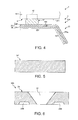
- Fig. 5 is a schematic transverse cross-sectional view illustrating a procedure of a step of a method (first embodiment) of manufacturing the liquid droplet ejecting head according to the embodiment of the invention.
- Fig. 6 is a schematic transverse cross-sectional view illustrating a procedure of a step of the method (first embodiment) of manufacturing the liquid droplet ejecting head according to the embodiment of the invention.
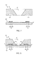
- Fig. 7 is a schematic transverse cross-sectional view illustrating a procedure of a step of the method (first embodiment) of manufacturing the liquid droplet ejecting head according to the embodiment of the invention.
- Fig. 8 is a schematic transverse cross-sectional view illustrating a procedure of a step of the method (first embodiment) of manufacturing the liquid droplet ejecting head according to the embodiment of the invention.
- Fig. 9 is a schematic transverse cross-sectional view illustrating a procedure of a step of the method (first embodiment) of manufacturing the liquid droplet ejecting head according to the embodiment of the invention.
- Fig. 10 is a schematic transverse cross-sectional view illustrating a procedure of a step of the method (first embodiment) of manufacturing the liquid droplet ejecting head according to the embodiment of the invention.
- Fig. 11 is a schematic transverse cross-sectional view illustrating a procedure of a step of the method (first embodiment) of manufacturing the liquid droplet ejecting head according to the embodiment of the invention.
- Fig. 12 is a schematic transverse cross-sectional view illustrating a procedure of a step of the method (first embodiment) of manufacturing the liquid droplet ejecting head according to the embodiment of the invention.
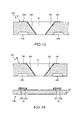
- Fig. 13 is a schematic transverse cross-sectional view illustrating a procedure of a step of a method (second embodiment) of manufacturing the liquid droplet ejecting head according to the embodiment of the invention.
- Fig. 14 is a schematic transverse cross-sectional view illustrating a procedure of a step of the method (second embodiment) of manufacturing the liquid droplet ejecting head according to the embodiment of the invention.
- Fig. 15 is a schematic transverse cross-sectional view illustrating a procedure of a step of the method (second embodiment) of manufacturing the liquid droplet ejecting head according to the embodiment of the invention.
- Fig. 16 is an enlarged detailed diagram of a region [D] surrounded by the chain line of Fig. 15 .
- Fig. 17 is a schematic transverse cross-sectional view illustrating a procedure of a step of the method (second embodiment) of manufacturing the liquid droplet ejecting head according to the embodiment of the invention.
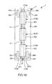
- Fig. 18 is a top plan view illustrating a liquid droplet ejecting head (third embodiment) according to the embodiment of the invention.
- Fig. 19 is a perspective view illustrating a printing apparatus according to the embodiment of the invention.
- liquid droplet ejecting head a liquid droplet ejecting head, a printing apparatus, and a method of manufacturing the liquid droplet ejecting head will be described in detail, on the basis of preferred embodiments of the invention, with reference to the accompanying drawings.
- Fig. 1 is a transverse cross-sectional view illustrating a liquid droplet ejecting head according to an embodiment of the invention.
- Fig. 2 is a diagram (top plan view) viewed from a direction of the arrow A of Fig. 1 .
- Fig. 3 is an enlarged detailed diagram of a region [B] surrounded by the chain line of Fig. 2 .
- Fig. 4 is an enlarged detailed diagram of a region [C] surrounded by the chain line of Fig. 1 .
- Figs. 5 to 12 are schematic transverse cross-sectional views illustrating a procedure of steps of a method (first embodiment) of manufacturing the liquid droplet ejecting head according to the embodiment of the invention.
- Fig. 5 to 12 are schematic transverse cross-sectional views illustrating a procedure of steps of a method (first embodiment) of manufacturing the liquid droplet ejecting head according to the embodiment of the invention.
- Fig. 1 is a transverse cross-sectional view illustrating a
- FIG. 19 is a perspective view illustrating a printing apparatus according to the embodiment of the invention. It should be noted that, hereinafter, for convenience of description, in Figs. 1 , 4 to 12 , and 19 (likewise, in Figs. 13 to 17 ), the upper side is referred to as “up” or “above”, and the lower side is referred to as “down” or "under”.
- a liquid droplet ejecting head 1 shown in Figs. 1 to 4 includes a base substrate 2, which is formed as a plate-like body, and an IC (Integrated Circuit) package 9 which is disposed on the base substrate 2. As described later, the liquid droplet ejecting head 1 is mounted in a printing apparatus (liquid droplet ejection apparatus) 100, and ejects an ink 300 as liquid droplets onto a printing medium 200 such as a printing paper, thereby performing printing on the printing medium 200 (refer to Fig. 19 ).
- a printing apparatus liquid droplet ejection apparatus
- the base substrate 2 is formed in a rectangular shape in plan view.
- the base substrate 2 has a sealing plate (first substrate) 10A, a device substrate (second substrate) 10B, and a nozzle substrate (nozzle plate) 21.
- the base substrate 2 is formed as a laminated body in which the nozzle substrate 21, the device substrate 10B, and the sealing plate 10A are laminated from the lower side in this order.
- the sealing plate 10A and the device substrate 10B are bonded through an adhesive layer (adhesive) 11.
- the thickness of the adhesive layer 11 is not particularly limited.
- the thickness is preferably in a range of 1 to 10 ⁇ m, and is more preferably in a range of 1 to 5 ⁇ m.
- the device substrate 10B and the nozzle substrate 21 are also bonded through an adhesive layer (not shown in the drawing).
- the sealing plate 10A is also formed as a laminated body, and has a reservoir formation substrate (protective substrate) 24, and a compliance substrate 26. Those are laminated from the lower side in this order.
- the device substrate 10B is also formed as a laminated body, and has a flow passage formation substrate 22, a vibration plate 23, and a plurality of piezoelectric elements 25. Those are laminated from the lower side in this order. Then, in each laminated body, layers constituting the laminated body are bonded through, for example, a thermal adhesion film, an adhesive layer, or the like not shown in the drawing.
- sealing plate itself and the device substrate themselves are also formed as a laminated body. Layers constituting the laminated body are bonded through, for example, a thermal adhesion film, an adhesive layer, or the like not shown in the drawing.
- the base substrate 2 is formed as a laminated body, the layers constituting the laminated body can be respectively employed in accordance with use applications and functions. Thereby, it is possible to obtain the low-profile liquid droplet ejecting head 1, and this contributes to a decrease in size of the printing apparatus 100.
- the nozzle substrate 21 has a plurality of ejection ports (nozzle openings) 211 which are formed through the nozzle substrate 21, that is, formed to be open toward the lower surface (the other surface) 212 of the base substrate 2 (plate-like body).
- ejection ports 211 are arranged in a matrix.
- the ejection ports 211 are arranged in n rows (n is an integer not less than 1) in the length direction (long side direction) of the base substrate 2 and in two columns in the width direction (short side direction).
- each ejection port 211 be provided with a coating layer with water repellency.
- the liquid droplets, which are ejected from the ejection ports 211 drop downward as vertically as possible, and can be reliably landed at landing target positions on the printing medium 200.
- a constituent material of the nozzle substrate 21 is not particularly limited, and it is preferable that the material be, for example, silicon material or stainless steel. Such a material is excellent in chemical resistance. Thus, even during exposure of the ink 300 over a long period of time, the nozzle substrate 21 can be reliably prevented from changing in quality and deteriorating. Furthermore, such a material is excellent in processability, and thus it is possible to obtain the nozzle substrate 21 with high dimensional accuracy. Hence, it is possible to obtain the liquid droplet ejecting head 1 with high reliability.
- the flow passages 221 are formed by performing, for example, etching. As shown in Fig. 1 , each flow passage 221 can be divided into a pressure generation chamber 222, a relay chamber (communication portion) 223, and a communication passage (supply passage) 224 through which the pressure generation chamber 222 communicates with the relay chamber 223.
- the pressure generation chamber 222 is provided to correspond to each ejection port 211, and communicates with the outside through the ejection port 211.
- the relay chamber 223 is provided upstream of the pressure generation chamber 222.
- the communication passage 224 is provided between the pressure generation chamber 222 and the relay chamber 223.
- constituent material of the flow passage formation substrate 22 is not particularly limited, and may employ, for example, the same constituent material as the nozzle substrate 21.
- the vibration plate 23 may be vibrated in the thickness direction by driving of the piezoelectric elements 25 to be described later. Further, some parts of the vibration plate 23 face the pressure generation chambers 222. Then, by vibrating the vibration plate 23, the pressures within the pressure generation chambers 222 are changed, and the ink 300 can be ejected as liquid droplets through the ejection ports 211 from the pressure generation chambers 222.
- Such a vibration plate 23 is formed by laminating an elastic film 231 and a lower electrode film 232 in order from the flow passage formation substrate 22 side.
- the elastic film 231 is formed of a silicon oxide film with a thickness of, for example, about 1 to 2 ⁇ m.
- the lower electrode film 232 is formed of a metal film with a thickness of, for example, about 0.2 ⁇ m.
- the lower electrode film 232 functions as a common electrode of the plurality of piezoelectric elements 25 which are disposed between the flow passage formation substrate 22 and the reservoir formation substrate 24.
- each reservoir 241 can be divided into a first chamber (reservoir section) 242, a second chamber (injection passage) 243, and a communication passage 244 through which the first chamber 242 communicates with the second chamber 243.
- the first chambers 242 are positioned above the relay chambers 223 of the flow passages 221 of the flow passage formation substrate 22. In addition, the parts of the vibration plate 23 between the first chambers 242 and the relay chambers 223 are penetrated. Thereby, each first chamber 242 communicates with each relay chamber 223.
- the second chamber 243 is provided upstream of the first chamber 242.
- the communication passage 244 is provided between the first chamber 242 and the second chamber 243.
- the relay chamber 223 may constitute a part of the reservoir 241.
- a piezoelectric element housing chambers 245, which respectively house the piezoelectric elements 25, is formed on the reservoir formation substrate 24.
- the piezoelectric element housing chamber 245 is formed separately from the reservoir 241.
- the constituent material of the reservoir formation substrate 24 is not particularly limited, and may employ, for example, silicon, glass, or the like.
- Each piezoelectric element 25 is formed by laminating a piezoelectric body film (piezo element) 251 and an upper electrode film 252 in order from the lower electrode film 232 side. Then, when a voltage is applied between the upper electrode film 252 and the lower electrode film 232, the piezoelectric body film 251 is deformed by the piezoelectric effect. Due to the deformation, the vibration plate 23 is vibrated in the up and down direction. As described above, due to the vibration of the vibration plate 23, the pressure within the pressure generation chamber 222 is changed, whereby the ink 300 can be ejected as liquid droplets through the ejection port 211 from the pressure generation chamber 222. As described above, each piezoelectric element 25 is configured to eject the ink 300 (liquid droplets) from the ejection port 211 through the vibration plate 23.
- the compliance substrate 26 is formed by laminating a sealing film 261 and a fixing plate 262 in order from the reservoir formation substrate 24 side.
- the sealing film 261 is formed of a material (for example, a polyphenylene sulfide film with a thickness of about 6 ⁇ m) with flexibility. Some parts of the sealing film 261 face the reservoirs 241.
- the fixing plate 262 is formed of a relatively hard material (for example, stainless steel with a thickness of about 30 ⁇ m) such as a metal material. It is preferable that absent portions 263 as vacant parts be formed on the parts of the fixing plate 262 facing the reservoir 241 side.
- injection ports 264 which penetrate through the sealing film 261 and the fixing plate 262, are formed on the compliance substrate 26. Each injection port 264 communicates with each reservoir 241 so as to inject the ink 300 into the reservoir 241.
- a concave portion 27 is formed on the base substrate 2 formed as the above-mentioned laminated body.
- the concave portion 27 is open toward the central portion of the upper surface (one surface) 265 of the sealing plate 10A (compliance substrate 26).
- the concave portion 27 is formed to penetrate the sealing plate 10A in the thickness direction through, for example, etching.
- the concave portion 27 is formed in a shape of a channel along the length direction of the base substrate 2. Then, the concave portion 27 is formed of a bottom portion 271, first side wall portions (side wall portions) 272a and 272b, and second side wall portions 273a and 273b.
- the first side wall portions 272a and 272b stand on the bottom portion 271, and are opposed to each other in a width direction of (a direction of intersecting with) the concave portion 27 (channel).
- the second side wall portions 273a and 273b stand on the bottom portion 271, and are opposed to each other in the length direction of the concave portion 27.
- the bottom portion 271 is a planar portion.
- the first side wall portions 272a and 272b are inclined to the bottom portion 271.
- the inclination angle is not particularly limited, but is, for example, 54.7 degrees to the plane of the bottom portion 271 when the reservoir formation substrate 24 is formed of silicon.
- the separation distance between the first side wall portions 272a and 272b gradually increases toward the upper surface 265 side.
- the second side wall portions 273a and 273b are inclined to the bottom portion 271, similarly to the first side wall portions 272a and 272b. Further, the separation distance between the second side wall portions 273a and 273b gradually increases toward the upper surface 265 side.
- the concave portion 27 can be easily and reliably formed by, for example, etching.
- the wiring pattern 28 is provided in the concave portion 27.
- the wiring pattern 28 is formed of multiple linear portions 281 each of which has a linear shape. Such linear portions 281 are arranged to be distributed on the first side wall portion 272a side and the first side wall portion 272b side, and are formed along a direction of inclination.
- the multiple linear portions 281, which are present on the first side wall portion 272a side, are separated from the multiple linear portions 281, which are present on the first side wall portion 272b side, in the width direction of the concave portion 27 (base substrate 2).
- the adjacent linear portions 281, which are present on the first side wall portion 272a side, are separated from each other in the length direction of the concave portion 27. That is, the linear portions 281 are arranged along the length direction of the concave portion 27 with spacings interposed therebetween. Furthermore, the spacings between the adjacent linear portions 281 gradually increase toward the bottom portion 271 side of the concave portion 27. By forming such spacings, the adjacent linear portions 281 are reliably prevented from being shorted (short-circuited) to each other, on the first side wall portion 272a side.
- the adjacent linear portions 281 which are present on the first side wall portion 272b side, are arranged along the length direction of the concave portion 27 with spacings interposed therebetween.
- the spacings between the adjacent linear portions 281 gradually increase toward the bottom portion 271 side of the concave portion 27. By forming such spacings, the adjacent linear portions 281 are reliably prevented from being shorted to each other, on the first side wall portion 272b side.
- each linear portion 281 is formed in a single line shape which is continuous from the upper surface 265 of the base substrate 2 to the bottom portion 271 of the concave portion 27.
- each linear portion 281 can be divided into an upper portion (first part) 282 which is formed on the upper surface 265, an intermediate portion (second part) 283 which is formed on the first side wall portion 272a (or first side wall portion 272b), and a lower portion (third part) 284 which is formed on the bottom portion 271.
- the lower portion 284 is connected to the upper electrode film 252.
- each linear portion 281 (wiring pattern 28) is formed by laminating a plurality of layers (a first layer 285 and a second layer 286 in the configuration shown in the drawing).
- Each of the first layer 285 and the second layer 286 is formed of a conductive material.
- the first layer 285 is formed of Ni-Cr
- the second layer 286 is formed of Au.
- Such a constituent material is a metal material with a relatively small electric resistance, and is preferred as the constituent material of the wiring pattern 28.
- the linear portion 281 is formed of two layers, and each layer can be employed in accordance with use applications and functions.
- each linear portion 281 is formed of two layers, but is not limited to this.
- each linear portion 281 may be formed of three or more layers.
- a conductive material such as Ni, Pd, Au, Ti, Ti-W, or Cu.
- the IC package 9 has an electronic circuit (semiconductor element) 91, a casing (package) 92 that houses the electronic circuit 91, and a plurality of terminals 93 that is exposed from the casing 92 and is electrically connected to the electronic circuit 91.
- the electronic circuit 91 is formed of, for example, semiconductors.
- the casing 92 is formed in a chip shape, and is able to house the electronic circuit 91 therein.
- the constituent material of the casing 92 is not particularly limited.
- the material includes various resin materials, various semiconductor materials, various metal materials, ceramics, or the like.
- Each terminal 93 is exposed on a front side surface (lower surface) 921 between the front side surface 921 and a rear side surface (upper surface) 922 of the casing 92 (IC package 9).
- front side surface is defined as, for example, a surface on which elements are formed.
- the number of the arranged terminals 93 is the same as the number of the linear portions 281 constituting the wiring pattern 28.
- each terminal 93 is able to come into contact with the upper portion 282 of the linear portion 281 corresponding to the terminal 93.
- the wiring pattern 28 is electrically connected to the terminals 93 through the connection members 12.
- the constituent material of the terminal 93 is not particularly limited, and may employ a metal material with a relatively small electric resistance such as gold or copper.
- each connection member 12 has a function of fixing the IC package 9 onto the base substrate 2.
- the liquid droplet ejecting head 1 can be formed to have a simple structure. As a result, the liquid droplet ejecting head 1 is made to have a small size.
- the IC package 9 having such a configuration is electrically connected to the piezoelectric elements 25 through the wiring pattern 28.
- the IC package 9 controls an operation of each piezoelectric element 25. Thereby, it is possible to precisely and reliably eject the ink 300.
- the single IC package 9 is disposed such that the front side surface 921 is set to face the concave portion 27 from the upper surface 265 side of the base substrate 2. Further, the width of the IC package 9 is greater than the width of the concave portion 27, and the IC package 9 is arranged over the concave portion 27 in the width direction.
- the IC package 9 may have a function of reinforcing a part of the base substrate 2 which is thinned by forming the concave portion 27.
- the total length (the length along the length direction of the concave portion 27) of the IC package 9 is shorter than the total length of the concave portion 27.
- the inside of the concave portion 27 is made to communicate with the outside. For example, it is possible to dissipate the heat of the inside of the concave portion 27.
- heat generated from the IC package 9 and the wiring pattern 28 is prevented from being trapped in the concave portion 27.
- each connection member 12 is disposed between each terminal 93 of the IC package 9 and each first part 282 of the wiring pattern 28.
- Each connection member 12 is formed as a protrusion (bump) made of a metal such as Au, Cu, or Ni.
- the connection member 12 and, for example, an Anisotropic Conductive Film (ACF) or an Anisotropic Conductive Paste (ACP), which is not shown, are interposed therebetween, and are pressed. In such a manner, the connection member 12 is reliably electrically connected. Further, otherwise, a Non-Conductive Paste (NCP) can be used. In this case, the connection member 12 is directly electrically connected to the first part 282. Thereby, the terminals 93 and the first parts 282 are reliably electrically connected through the connection members 12.
- ACF Anisotropic Conductive Film
- ACP Anisotropic Conductive Paste
- Figs. 5 to 12 are schematic diagrams illustrating a principal section of the liquid droplet ejecting head 1.
- the manufacturing method includes a first preparation step (refer to Fig. 5 ), a first etching step (refer to Fig. 6 ), a second preparation step (refer to Fig. 7 ), a first bonding step (refer to Fig. 8 ), a wiring pattern forming step (refer to Fig. 9 ), a second etching step (refer to Fig. 10 ), a second bonding step (refer to Fig. 11 ), and a mounting step (refer to Fig. 12 ).
- a plate-like base material 24' to form a reservoir formation substrate 24 is provided.
- the base material 24' is a plate member which is formed of silicon and of which the thickness is 400 ⁇ m.
- Fig. 6 anisotropic wet etching is performed on the base material 24', and the concave portion 27, the piezoelectric element housing chamber 245, and the like are formed, thereby forming the reservoir formation substrate 24. It should be noted that, although omitted in Fig. 6 (the same in Figs. 7 to 12 ), in the process flow, the reservoir 241 is also formed.
- the base material 24' is thermally oxidized, and a SiO 2 film with a thickness of, for example 700 nm, is formed on the outer surface of the base material 24'. Subsequently, both surfaces of the base material 24' are coated with a resist, and patterning is performed thereon. Then, by dipping the base material 24' into hydrofluoric acid, a part of the SiO 2 film is removed, and the outer surface of the base material 24' is exposed.
- the resist is exfoliated, the base material 24' is dipped into KOH solution with a concentration of 35%, and the concave portion 27, the piezoelectric element housing chamber 245, and the like are formed on the base material 24'. Thereby, it is possible to obtain the reservoir formation substrate 24. Subsequently, after the SiO 2 film is etched by the hydrofluoric acid, the reservoir formation substrate 24 is thermally oxidized again, thereby insulating the outer surface of the reservoir formation substrate 24.
- an intermediate component 10B' forming the device substrate 10B is provided.
- the intermediate component 10B' is a component in which the flow passage 221 is not formed on the base material 22' forming the flow passage formation substrate 22. It should be noted that, although omitted in Fig. 7 (the same in Figs. 8 to 12 ), the vibration plate 23 is also disposed on the intermediate component 10B' (device substrate 10B).
- the opposite side surface to the side on which the concave portion 27 of the reservoir formation substrate 24 is open that is, the entire lower surface is coated with an adhesive
- the reservoir formation substrate 24 (sealing plate 10A) and the intermediate component 10B' are bonded through the adhesive layer 11.
- a part 111 of the adhesive layer 11 project from the boundary portion between the reservoir formation substrate 24 and the intermediate component 10B' in the concave portion 27.
- the wiring pattern 28 is formed at a position to form the wiring pattern 28. That is, the upper portion 282 is formed on the upper surface 265, the intermediate portion 283 is formed on the first side wall portion 272a (or first side wall portion 272b), and the lower portion 284 is formed on the bottom portion 271.
- the metal film is a film in which the Ni-Cr layer (first layer 285) with a thickness of for example 50 nm and the Au layer (second layer 286) with a thickness of 700 nm formed on the Ni-Cr layer are laminated.
- the resist is formed on the metal film.
- the resist is patterned by photolithography (exposure, development). Thereafter, the wet etching is sequentially performed on the Au layer and the Ni-Cr layer.
- an etchant for the Au layer an iodine-based etchant is used.
- an etchant for the Ni-Cr layer a nitric-acid-based or hydrochloric-acid-based etchant is used. Subsequently, the resist is exfoliated. Thereby, the wiring pattern 28 is formed.
- the base material 22' of the intermediate component 10B' is etched, and as shown in Fig. 10 , the flow passage 221 is formed on the base material 22'. Thereby, it is possible to obtain the device substrate 10B. It should be noted that, although omitted in Fig. 10 (the same in Figs. 11 and 12 ), the relay chamber 223 and the communication passage 224 constituting the flow passage 221 are formed.
- the nozzle substrate 21 is bonded to the lower surface of the device substrate 10B through, for example, adhesion (adhesion using an adhesive or a solvent). Thereby, it is possible to obtain the base substrate 2.
- the compliance substrate 26 is bonded to the reservoir formation substrate 24 through adhesion (adhesion using an adhesive or a solvent). It should be noted that, in Fig. 11 (the same in Fig. 12 ), the compliance substrate 26 is omitted.
- the IC package 9 is mounted on the base substrate 2.
- each connection member 12 is provided for each terminal 93 of the IC package 9.
- the connection member 12 is formed of an Au bump.
- the IC package 9, on which the connection members 12 are formed is disposed such that the front side surface 921 faces the concave portion 27 of the base substrate 2, and each terminal 93 of the IC package 9 is electrically connected to the upper portion 282 of each linear portion 281 of the wiring pattern 28 through the connection member 12 and the ACF.
- the connection members 12 are heated at a temperature of 170 degrees or less.
- the single reservoir formation substrate 24 is obtained from the single base material 24', thereby manufacturing the base substrate 2.
- a plurality of reservoir formation substrates 24 may be obtained from the single base material 24', and a plurality of intermediate components 10B' may be bonded and be thereafter cut (divided) into each intermediate component 10B', whereby the base substrate 2 can be manufactured.
- the printing apparatus 100 shown in Fig. 19 is a printing apparatus that performs printing on the printing medium 200 in an ink jet method.
- the printing apparatus 100 includes: an apparatus main body 50, printing head units 20A and 20B on which the liquid droplet ejecting head 1 is mounted; ink cartridges 30A and 30B that supply the ink 300; a carriage 40 that transports the printing head units 20A and 20B; a moving mechanism 70 that moves the carriage 40; and a carriage shaft 60 that movably supports (guides) the carriage 40.
- the ink cartridge 30A is detachably mounted on the printing head unit 20A, and is able to supply the ink 300 (black ink composition) to the printing head unit 20A in the mounting state.
- the ink cartridge 30B is also detachably mounted on the printing head unit 20B, and is able to supply the ink 300 (color ink composition) to the printing head unit 20B in the mounting state.
- the moving mechanism 70 has a driving motor 701 and a timing belt 702 which is connected to the driving motor 701. Then, a driving force (torque) of the driving motor 701 is transferred to the carriage 40 through the timing belt 702, whereby it is possible to move the carriage 40 along the direction of the carriage shaft 60 together with the printing head units 20A and 20B.
- a platen 80 is provided on the lower side of the carriage shaft 60 along the shaft direction.
- the printing medium 200 which is fed by a sheet feeding roller not shown in the drawing, is transported onto the platen 80. Then, the ink 300 is ejected onto the printing medium 200 on the platen 80, thereby performing printing.
- the liquid droplet ejecting head 1 is miniaturized. Then, the printing apparatus 100 having the liquid droplet ejecting head 1 is also miniaturized.
- Figs. 13 to 15 and 17 are schematic transverse cross-sectional views illustrating a procedure of steps of the method (second embodiment) of manufacturing the liquid droplet ejecting head according to the embodiment of the invention.
- Fig. 16 is an enlarged detailed diagram of a region [D] surrounded by the chain line of Fig. 15 .
- the present embodiment is the same as the first embodiment except that some steps of the method of manufacturing the liquid droplet ejecting head are different.
- Figs. 13 to 17 are schematic diagrams illustrating a principal section of the liquid droplet ejecting head 1.
- the manufacturing method is the same as the manufacturing method of the first embodiment in the first preparation step, the first etching step, and the second etching step to the mounting step.
- the manufacturing method of the present embodiment is different from that of the first embodiment in the steps between the first etching step and the second etching step.
- the different steps are the first wiring pattern forming step (refer to Fig. 13 ), the second preparation step (refer to Fig. 14 ), the first bonding step (refer to Figs. 15 and 16 ), and the second wiring pattern forming step (refer to Fig. 17 ).
- the upper portions 282 constituting a part of the wiring pattern 28 are formed on the upper surface 265, and the intermediate portions 283 are formed on the first side wall portion 272a (or the first side wall portion 272b).
- a metal film is formed by sputtering on the upper side surface of the sealing plate 10A, that is, the entire front side surface.
- the metal film is a film in which the Ni-Cr layer (first layer 285) with a thickness of for example 50 nm and the Au layer (second layer 286) with a thickness of 700 nm formed on the Ni-Cr layer are laminated.
- the resist is formed on the metal film.
- the resist is patterned by photolithography (exposure, development). Thereafter, the wet etching is sequentially performed on the Au layer and the Ni-Cr layer.
- an etchant for the Au layer an iodine-based etchant is used.
- a nitric-acid-based or hydrochloric-acid-based etchant is used as an etchant for the Ni-Cr layer. Subsequently, the resist is exfoliated. Thereby, the upper portions 282 and the intermediate portions 283 are formed.
- the intermediate component 10B' forming the device substrate 10B is provided.
- the opposite side surface to the side on which the concave portion 27 of the reservoir formation substrate 24 is open that is, the entire lower surface is coated with an adhesive, and as shown in Figs. 15 and 16 , the reservoir formation substrate 24 (sealing plate 10A) and the intermediate component 10B' are bonded through the adhesive layer 11.
- the adhesive layer 11 it is preferable that a part 111 of the adhesive layer 11 do not project from the boundary portion between the reservoir formation substrate 24 and the intermediate component 10B' in the concave portion 27.
- the bonding is performed to align each intermediate portion 283 and the upper electrode film 252 of each piezoelectric element 25 (refer to Fig. 16 ).
- the bonded body in which the sealing plate 10A and the intermediate component 10B' are bonded, is dipped into an electroless plating solution, and a plated metal is deposited on the metal films (the upper portions 282, the intermediate portions 283, and the upper electrode film 252) on the bonded body.
- the Ni plated layer 287 and the Au plated layer 288 are laminated.
- the intermediate portions 283 and the upper electrode film 252 are connected through the plating.
- each linear portion 281 is reliably electrically connected to the upper electrode film 252 of each piezoelectric element 25.
- Fig. 18 is a top plan view illustrating a liquid droplet ejecting head (third embodiment) according to the embodiment of the invention.
- the present embodiment is the same as the first embodiment except that the disposition number of the IC packages is different.
- a plurality of (three in the configuration shown in the drawing) the IC packages 9 are disposed along the length direction of the concave portion 27 which is formed in a channel shape. Further, gaps 13 are formed between the adjacent IC packages 9. Through the gaps 13, it is possible to discharge heat within the concave portion 27.
- the disposition number of the IC packages 9 is three in the configuration shown in the drawing. However, the invention is not limited to this. For example, the number may be two or four or more.
- each portion which constitutes the liquid droplet ejecting head and the printing apparatus, can be replaced with an arbitrary component capable of exhibiting the same function. Further, an arbitrary component may be added.
- the liquid droplet ejecting head is configured so as to eject the ink as liquid droplets onto the printing medium such as the printing paper, thereby performing printing.
- the invention is not limited to this.
- a liquid crystal display device (LCD device) may be manufactured by ejecting a material, which is for forming the liquid crystal display device, as liquid droplets.
- an organic electroluminescence display device (organic EL device) may be manufactured by ejecting a material, which is for forming the organic EL device, as liquid droplets.
- a circuit substrate may be manufactured by ejecting a material, which is for forming the wiring pattern, as liquid droplets so as to form the wiring pattern of an electronic circuit.
Landscapes
- Engineering & Computer Science (AREA)
- Manufacturing & Machinery (AREA)
- Particle Formation And Scattering Control In Inkjet Printers (AREA)
Abstract
Description
- The present invention relates to a liquid droplet ejecting head, a printing apparatus, and a method of manufacturing the liquid droplet ejecting head.
- For example, to perform printing on a printing medium such as a printing paper, a printing apparatus, which has a liquid droplet ejecting head, is used (for example, refer to
JP-A-2006-289943 -
JP-A-2006-289943 - Further, in the liquid droplet ejecting head disclosed in
JP-A-2006-289943 - Meanwhile, recently, there has been a demand for a decrease in size of the liquid droplet ejecting head. Hence, it is also necessary to decrease the size of the base substrate. However, when the size of the base substrate is decreased, in the known disposition, it may be difficult to arrange the driver ICs on the base substrate. When the driver ICs are intended to be arranged, while a space for disposition of the driver ICs is secured, the space may be made to be as small as possible. Even in this case, there is a problem in that it is difficult to sufficiently decrease the size of the liquid droplet ejecting head.
- An advantage of some aspects of the invention is to provide a liquid droplet ejecting head capable of achieving a decrease in size, a printing apparatus having the liquid droplet ejecting head, and a method of manufacturing the liquid droplet ejecting head.
- An aspect of the invention is directed to a liquid droplet ejecting head including: a base substrate of a plate-like body that has a concave portion that is formed to be open toward one surface and a wiring pattern made of a conductive material; and an IC package that is electrically connected to the wiring pattern, in which the concave portion has a bottom portion and two side wall portions, which stand on the bottom portion so as to be opposed to each other, and the two side wall portions are inclined such that a separation distance between the two side wall portions gradually increases toward the one surface side, in which the wiring pattern has a plurality of linear objects, each of which is continuous and is constituted of a first part formed on the one surface, a second part formed on the side wall portion, and a third part formed on the bottom portion, and in which the IC package is formed in a chip shape, has a plurality of terminals which are formed on a surface opposed to the concave portion, and each terminal is electrically connected to the first part.
- With this configuration, it is possible to minimize the space for disposition of the IC package on the base substrate. Therefore, it is possible to reliably decrease the size of the liquid droplet ejecting head. Further, for example, when a plurality of piezoelectric elements for ejecting the liquid droplets can be controlled with a single IC package, the configuration is further advantageous in decreasing the size of the liquid droplet ejecting head.
- In the liquid droplet ejecting head of the aspect of the invention, it is preferable that the linear objects are arranged to be distributed on both sides of the two side wall portions.
- With this configuration, the multiple (plural) linear objects constituting the wiring pattern can be reliably arranged. Consequently, the IC package, which is capable of transmitting and receiving a large volume of information through the linear objects, can be mounted on the base substrate.
- In the liquid droplet ejecting head of the aspect of the invention, it is preferable that the concave portion is formed in a shape of a channel, and the two side wall portions are opposed to each other in a direction of intersecting with the channel.
- With this configuration, the multiple (plural) linear objects constituting the wiring pattern can be reliably arranged. Consequently, the IC package, which is capable of transmitting and receiving a large volume of information through the linear objects, can be mounted on the base substrate.
- In the liquid droplet ejecting head of the aspect of the invention, it is preferable that the linear objects are disposed with spacings interposed therebetween along a direction of the channel.
- With this configuration, the linear objects, which are adjacent in the length direction of the channel, are more reliably prevented from being shorted (short-circuited) to each other.
- In the liquid droplet ejecting head of the aspect of the invention, it is preferable that the linear object spacings neighboring to one another increase from the one surface side toward the bottom portion side.
- With this configuration, the linear objects, which are adjacent in the length direction of the channel, are more reliably prevented from being shorted (short-circuited) to each other.
- In the liquid droplet ejecting head of the aspect of the invention, it is preferable that a length of the IC package in a direction of the channel is shorter than a total length of the channel.
- With this configuration, the inside of the concave portion is made to communicate with the outside. With such a configuration, for example, it is possible to dissipate the heat of the inside of the concave portion. Thus, heat generated from the IC package and the wiring is prevented from being trapped in the concave portion.
- In the liquid droplet ejecting head of the aspect of the invention, it is preferable that a plurality of the IC packages are disposed with spacings interposed therebetween in a direction of the channel.
- With this configuration, it is possible to dissipate the heat of the inside of the concave portion (channel) from the spacings between the IC packages.
- In the liquid droplet ejecting head of the aspect of the invention, it is preferable that a connection member containing a conductive material is disposed between each terminal and each first part, each terminal is electrically connected to each first part through the connection member, and the connection member has a function of fixing the IC package onto the base substrate.
- With this configuration, it is not necessary to separately provide a fixing member for fixing the IC package onto the base substrate. Thus, the liquid droplet ejecting head can be formed to have a simple structure. As a result, the liquid droplet ejecting head is made to have a small size.
- In the liquid droplet ejecting head of the aspect of the invention, it is preferable that the base substrate has an ejection port, which is formed to be open toward the other surface of the plate-like body and ejects liquid droplets, and a piezoelectric element which causes the liquid droplets to be ejected from the ejection port, and the IC package is electrically connected to the piezoelectric element through the wiring pattern so as to control an operation of the piezoelectric element.
- With this configuration, for example, it is possible to precisely and reliably control the ejection conditions such as an amount of ejected liquid droplets and ejection timing (ejection and stop of the ejection).
- In the liquid droplet ejecting head of the aspect of the invention, it is preferable that the base substrate has a first plate-like body that has the concave portion, and a second plate-like body that is bonded to an opposite side to a side, on which the concave portion of the first plate-like body is open, and that has the piezoelectric element, and the first plate-like body and the second plate-like body are bonded through an adhesive.
- With this configuration, the first plate-like body and the second plate-like body can be respectively employed in accordance with use applications and functions. Accordingly, it is possible to obtain a low-profile (small-sized) liquid droplet ejecting head. When the liquid droplet ejecting head is provided in a printing apparatus, this contributes to a decrease in size of the printing apparatus.
- In the liquid droplet ejecting head of the aspect of the invention, it is preferable that the wiring pattern is formed of a plurality of layers which are laminated.
- With this configuration, the layers constituting the wiring pattern can be respectively employed in accordance with use applications and functions. Thus, this configuration is advantageous in decreasing the size of the liquid droplet ejecting head.
- Another aspect of the invention is directed to a printing apparatus including the liquid droplet ejecting head according to the above-mentioned aspect of the invention.
- With this configuration, it is possible to provide the printing apparatus having the small-sized liquid droplet ejecting head.
- Still another aspect of the invention is directed to a method of manufacturing the liquid droplet ejecting head, in which the base substrate has a first plate-like body that has the concave portion, and a second plate-like body that is bonded to an opposite side to a side, on which the concave portion of the first plate-like body is open, and that has a piezoelectric element which is electrically connected to the IC package through the wiring pattern, in which the method includes: a step of bonding the first plate-like body and the second plate-like body; a step of forming a wiring pattern by forming the first part on the one surface, forming the second part on the side wall portion, and forming the third part on the bottom portion; and a step of mounting the IC package such that the front side surface of the IC package faces the concave portion and each terminal is electrically connected to each first part.
- With this configuration, it is possible to reliably manufacture the liquid droplet ejecting head capable of achieving a decrease in size. Thus, for example, by mounting the liquid droplet ejecting head in the printing apparatus, it is possible to provide a small-sized printing apparatus.
- Yet another aspect of the invention is directed to a method of manufacturing the liquid droplet ejecting head, in which the base substrate has a first plate-like body that has the concave portion, and a second plate-like body that is bonded to an opposite side to a side, on which the concave portion of the first plate-like body is open, and that has a piezoelectric element which is electrically connected to the IC package through the wiring pattern, and in which the method includes: forming a first wiring pattern by forming the first part on the one surface and forming the second part on the side wall portion; bonding the first plate-like body and the second plate-like body; forming a second wiring pattern by forming the third part on the bottom portion; and mounting the IC package such that the front side surface of the IC package faces the concave portion and each terminal is electrically connected to each first part.
- With this configuration, it is possible to reliably manufacture the liquid droplet ejecting head capable of achieving a decrease in size. Thus, for example, by mounting the liquid droplet ejecting head in the printing apparatus, it is possible to provide a small-sized printing apparatus.
- The invention will be described with reference to the accompanying drawings, wherein like numbers reference like elements.
-
Fig. 1 is a transverse cross-sectional view illustrating a liquid droplet ejecting head according to an embodiment of the invention. -
Fig. 2 is a diagram (top plan view) viewed from a direction of the arrow A ofFig. 1 . -
Fig. 3 is an enlarged detailed diagram of a region [B] surrounded by the chain line ofFig. 2 . -
Fig. 4 is an enlarged detailed diagram of a region [C] surrounded by the chain line ofFig. 1 . -
Fig. 5 is a schematic transverse cross-sectional view illustrating a procedure of a step of a method (first embodiment) of manufacturing the liquid droplet ejecting head according to the embodiment of the invention. -
Fig. 6 is a schematic transverse cross-sectional view illustrating a procedure of a step of the method (first embodiment) of manufacturing the liquid droplet ejecting head according to the embodiment of the invention. -
Fig. 7 is a schematic transverse cross-sectional view illustrating a procedure of a step of the method (first embodiment) of manufacturing the liquid droplet ejecting head according to the embodiment of the invention. -
Fig. 8 is a schematic transverse cross-sectional view illustrating a procedure of a step of the method (first embodiment) of manufacturing the liquid droplet ejecting head according to the embodiment of the invention. -
Fig. 9 is a schematic transverse cross-sectional view illustrating a procedure of a step of the method (first embodiment) of manufacturing the liquid droplet ejecting head according to the embodiment of the invention. -
Fig. 10 is a schematic transverse cross-sectional view illustrating a procedure of a step of the method (first embodiment) of manufacturing the liquid droplet ejecting head according to the embodiment of the invention. -
Fig. 11 is a schematic transverse cross-sectional view illustrating a procedure of a step of the method (first embodiment) of manufacturing the liquid droplet ejecting head according to the embodiment of the invention. -
Fig. 12 is a schematic transverse cross-sectional view illustrating a procedure of a step of the method (first embodiment) of manufacturing the liquid droplet ejecting head according to the embodiment of the invention. -
Fig. 13 is a schematic transverse cross-sectional view illustrating a procedure of a step of a method (second embodiment) of manufacturing the liquid droplet ejecting head according to the embodiment of the invention. -
Fig. 14 is a schematic transverse cross-sectional view illustrating a procedure of a step of the method (second embodiment) of manufacturing the liquid droplet ejecting head according to the embodiment of the invention. -
Fig. 15 is a schematic transverse cross-sectional view illustrating a procedure of a step of the method (second embodiment) of manufacturing the liquid droplet ejecting head according to the embodiment of the invention. -
Fig. 16 is an enlarged detailed diagram of a region [D] surrounded by the chain line ofFig. 15 . -
Fig. 17 is a schematic transverse cross-sectional view illustrating a procedure of a step of the method (second embodiment) of manufacturing the liquid droplet ejecting head according to the embodiment of the invention. -
Fig. 18 is a top plan view illustrating a liquid droplet ejecting head (third embodiment) according to the embodiment of the invention. -
Fig. 19 is a perspective view illustrating a printing apparatus according to the embodiment of the invention. - Hereinafter, a liquid droplet ejecting head, a printing apparatus, and a method of manufacturing the liquid droplet ejecting head will be described in detail, on the basis of preferred embodiments of the invention, with reference to the accompanying drawings.
-
Fig. 1 is a transverse cross-sectional view illustrating a liquid droplet ejecting head according to an embodiment of the invention.Fig. 2 is a diagram (top plan view) viewed from a direction of the arrow A ofFig. 1 .Fig. 3 is an enlarged detailed diagram of a region [B] surrounded by the chain line ofFig. 2 .Fig. 4 is an enlarged detailed diagram of a region [C] surrounded by the chain line ofFig. 1 .Figs. 5 to 12 are schematic transverse cross-sectional views illustrating a procedure of steps of a method (first embodiment) of manufacturing the liquid droplet ejecting head according to the embodiment of the invention.Fig. 19 is a perspective view illustrating a printing apparatus according to the embodiment of the invention. It should be noted that, hereinafter, for convenience of description, inFigs. 1 ,4 to 12 , and19 (likewise, inFigs. 13 to 17 ), the upper side is referred to as "up" or "above", and the lower side is referred to as "down" or "under". - A liquid
droplet ejecting head 1 shown inFigs. 1 to 4 includes abase substrate 2, which is formed as a plate-like body, and an IC (Integrated Circuit)package 9 which is disposed on thebase substrate 2. As described later, the liquiddroplet ejecting head 1 is mounted in a printing apparatus (liquid droplet ejection apparatus) 100, and ejects anink 300 as liquid droplets onto aprinting medium 200 such as a printing paper, thereby performing printing on the printing medium 200 (refer toFig. 19 ). - As shown in
Fig. 2 , thebase substrate 2 is formed in a rectangular shape in plan view. Thebase substrate 2 has a sealing plate (first substrate) 10A, a device substrate (second substrate) 10B, and a nozzle substrate (nozzle plate) 21. Thebase substrate 2 is formed as a laminated body in which thenozzle substrate 21, thedevice substrate 10B, and the sealingplate 10A are laminated from the lower side in this order. Further, the sealingplate 10A and thedevice substrate 10B are bonded through an adhesive layer (adhesive) 11. The thickness of theadhesive layer 11 is not particularly limited. For example, the thickness is preferably in a range of 1 to 10 µm, and is more preferably in a range of 1 to 5 µm. Furthermore, thedevice substrate 10B and thenozzle substrate 21 are also bonded through an adhesive layer (not shown in the drawing). - The sealing
plate 10A is also formed as a laminated body, and has a reservoir formation substrate (protective substrate) 24, and acompliance substrate 26. Those are laminated from the lower side in this order. Further, thedevice substrate 10B is also formed as a laminated body, and has a flowpassage formation substrate 22, a vibration plate 23, and a plurality ofpiezoelectric elements 25. Those are laminated from the lower side in this order. Then, in each laminated body, layers constituting the laminated body are bonded through, for example, a thermal adhesion film, an adhesive layer, or the like not shown in the drawing. - Further, the sealing plate itself and the device substrate themselves are also formed as a laminated body. Layers constituting the laminated body are bonded through, for example, a thermal adhesion film, an adhesive layer, or the like not shown in the drawing.
- As described above, since the
base substrate 2 is formed as a laminated body, the layers constituting the laminated body can be respectively employed in accordance with use applications and functions. Thereby, it is possible to obtain the low-profile liquiddroplet ejecting head 1, and this contributes to a decrease in size of theprinting apparatus 100. - As shown in
Fig. 1 , thenozzle substrate 21 has a plurality of ejection ports (nozzle openings) 211 which are formed through thenozzle substrate 21, that is, formed to be open toward the lower surface (the other surface) 212 of the base substrate 2 (plate-like body).Such ejection ports 211 are arranged in a matrix. As shown inFig. 2 , in the embodiment, theejection ports 211 are arranged in n rows (n is an integer not less than 1) in the length direction (long side direction) of thebase substrate 2 and in two columns in the width direction (short side direction). - In addition, it is preferable that each
ejection port 211 be provided with a coating layer with water repellency. Thereby, the liquid droplets, which are ejected from theejection ports 211, drop downward as vertically as possible, and can be reliably landed at landing target positions on theprinting medium 200. - Further, a constituent material of the
nozzle substrate 21 is not particularly limited, and it is preferable that the material be, for example, silicon material or stainless steel. Such a material is excellent in chemical resistance. Thus, even during exposure of theink 300 over a long period of time, thenozzle substrate 21 can be reliably prevented from changing in quality and deteriorating. Furthermore, such a material is excellent in processability, and thus it is possible to obtain thenozzle substrate 21 with high dimensional accuracy. Hence, it is possible to obtain the liquiddroplet ejecting head 1 with high reliability. - Flow passages (cavities) 221, through which the
ink 300 is sent to therespective ejection ports 211, are formed on the flowpassage formation substrate 22. Theflow passages 221 are formed by performing, for example, etching. As shown inFig. 1 , eachflow passage 221 can be divided into apressure generation chamber 222, a relay chamber (communication portion) 223, and a communication passage (supply passage) 224 through which thepressure generation chamber 222 communicates with therelay chamber 223. - The
pressure generation chamber 222 is provided to correspond to eachejection port 211, and communicates with the outside through theejection port 211. - The
relay chamber 223 is provided upstream of thepressure generation chamber 222. - The
communication passage 224 is provided between thepressure generation chamber 222 and therelay chamber 223. - In addition, the constituent material of the flow
passage formation substrate 22 is not particularly limited, and may employ, for example, the same constituent material as thenozzle substrate 21. - The vibration plate 23 may be vibrated in the thickness direction by driving of the
piezoelectric elements 25 to be described later. Further, some parts of the vibration plate 23 face thepressure generation chambers 222. Then, by vibrating the vibration plate 23, the pressures within thepressure generation chambers 222 are changed, and theink 300 can be ejected as liquid droplets through theejection ports 211 from thepressure generation chambers 222. - Such a vibration plate 23 is formed by laminating an elastic film 231 and a
lower electrode film 232 in order from the flowpassage formation substrate 22 side. The elastic film 231 is formed of a silicon oxide film with a thickness of, for example, about 1 to 2 µm. Thelower electrode film 232 is formed of a metal film with a thickness of, for example, about 0.2 µm. Thelower electrode film 232 functions as a common electrode of the plurality ofpiezoelectric elements 25 which are disposed between the flowpassage formation substrate 22 and thereservoir formation substrate 24. - In the
reservoir formation substrate 24, thereservoirs 241, which temporarily store theink 300, are formed to respectively communicate with theflow passages 221 of the flowpassage formation substrate 22. As shown inFig. 1 , eachreservoir 241 can be divided into a first chamber (reservoir section) 242, a second chamber (injection passage) 243, and acommunication passage 244 through which thefirst chamber 242 communicates with thesecond chamber 243. - The
first chambers 242 are positioned above therelay chambers 223 of theflow passages 221 of the flowpassage formation substrate 22. In addition, the parts of the vibration plate 23 between thefirst chambers 242 and therelay chambers 223 are penetrated. Thereby, eachfirst chamber 242 communicates with eachrelay chamber 223. - The
second chamber 243 is provided upstream of thefirst chamber 242. - The
communication passage 244 is provided between thefirst chamber 242 and thesecond chamber 243. - It should be noted that, in the liquid
droplet ejecting head 1, therelay chamber 223 may constitute a part of thereservoir 241. - Further, a piezoelectric
element housing chambers 245, which respectively house thepiezoelectric elements 25, is formed on thereservoir formation substrate 24. The piezoelectricelement housing chamber 245 is formed separately from thereservoir 241. - The constituent material of the
reservoir formation substrate 24 is not particularly limited, and may employ, for example, silicon, glass, or the like. - Each
piezoelectric element 25 is formed by laminating a piezoelectric body film (piezo element) 251 and anupper electrode film 252 in order from thelower electrode film 232 side. Then, when a voltage is applied between theupper electrode film 252 and thelower electrode film 232, thepiezoelectric body film 251 is deformed by the piezoelectric effect. Due to the deformation, the vibration plate 23 is vibrated in the up and down direction. As described above, due to the vibration of the vibration plate 23, the pressure within thepressure generation chamber 222 is changed, whereby theink 300 can be ejected as liquid droplets through theejection port 211 from thepressure generation chamber 222. As described above, eachpiezoelectric element 25 is configured to eject the ink 300 (liquid droplets) from theejection port 211 through the vibration plate 23. - The
compliance substrate 26 is formed by laminating asealing film 261 and a fixingplate 262 in order from thereservoir formation substrate 24 side. The sealingfilm 261 is formed of a material (for example, a polyphenylene sulfide film with a thickness of about 6 µm) with flexibility. Some parts of the sealingfilm 261 face thereservoirs 241. Further, the fixingplate 262 is formed of a relatively hard material (for example, stainless steel with a thickness of about 30 µm) such as a metal material. It is preferable thatabsent portions 263 as vacant parts be formed on the parts of the fixingplate 262 facing thereservoir 241 side. - Further,
injection ports 264, which penetrate through the sealingfilm 261 and the fixingplate 262, are formed on thecompliance substrate 26. Eachinjection port 264 communicates with eachreservoir 241 so as to inject theink 300 into thereservoir 241. - As shown in
Fig. 1 , aconcave portion 27 is formed on thebase substrate 2 formed as the above-mentioned laminated body. Theconcave portion 27 is open toward the central portion of the upper surface (one surface) 265 of the sealingplate 10A (compliance substrate 26). Theconcave portion 27 is formed to penetrate the sealingplate 10A in the thickness direction through, for example, etching. - Further, as shown in
Figs. 1 and2 , theconcave portion 27 is formed in a shape of a channel along the length direction of thebase substrate 2. Then, theconcave portion 27 is formed of abottom portion 271, first side wall portions (side wall portions) 272a and 272b, and secondside wall portions side wall portions bottom portion 271, and are opposed to each other in a width direction of (a direction of intersecting with) the concave portion 27 (channel). The secondside wall portions bottom portion 271, and are opposed to each other in the length direction of theconcave portion 27. Thereby, linear portions (linear objects) 281, which constitute awiring pattern 28 electrically connected to theIC package 9 to be described later, are distributed on both sides of the firstside wall portions linear portions 281 can be arranged along the length direction of the concave portion 27 (channel) (refer toFig. 3 ). Consequently, theIC package 9, which is capable of transmitting and receiving a large volume of information through thelinear portions 281, can be mounted on the base substrate. - The
bottom portion 271 is a planar portion. - The first
side wall portions bottom portion 271. In addition, the inclination angle is not particularly limited, but is, for example, 54.7 degrees to the plane of thebottom portion 271 when thereservoir formation substrate 24 is formed of silicon. Further, the separation distance between the firstside wall portions upper surface 265 side. - The second
side wall portions bottom portion 271, similarly to the firstside wall portions side wall portions upper surface 265 side. - As described above, the first
side wall portions side wall portions concave portion 27 can be easily and reliably formed by, for example, etching. - As shown in
Figs. 1 and3 , thewiring pattern 28 is provided in theconcave portion 27. Thewiring pattern 28 is formed of multiplelinear portions 281 each of which has a linear shape. Suchlinear portions 281 are arranged to be distributed on the firstside wall portion 272a side and the firstside wall portion 272b side, and are formed along a direction of inclination. - Further, the multiple
linear portions 281, which are present on the firstside wall portion 272a side, are separated from the multiplelinear portions 281, which are present on the firstside wall portion 272b side, in the width direction of the concave portion 27 (base substrate 2). - As shown in
Fig. 3 , the adjacentlinear portions 281, which are present on the firstside wall portion 272a side, are separated from each other in the length direction of theconcave portion 27. That is, thelinear portions 281 are arranged along the length direction of theconcave portion 27 with spacings interposed therebetween. Furthermore, the spacings between the adjacentlinear portions 281 gradually increase toward thebottom portion 271 side of theconcave portion 27. By forming such spacings, the adjacentlinear portions 281 are reliably prevented from being shorted (short-circuited) to each other, on the firstside wall portion 272a side. - Likewise, the adjacent
linear portions 281, which are present on the firstside wall portion 272b side, are arranged along the length direction of theconcave portion 27 with spacings interposed therebetween. In addition, the spacings between the adjacentlinear portions 281 gradually increase toward thebottom portion 271 side of theconcave portion 27. By forming such spacings, the adjacentlinear portions 281 are reliably prevented from being shorted to each other, on the firstside wall portion 272b side. - As shown in
Figs. 1 and3 , eachlinear portion 281 is formed in a single line shape which is continuous from theupper surface 265 of thebase substrate 2 to thebottom portion 271 of theconcave portion 27. In addition, eachlinear portion 281 can be divided into an upper portion (first part) 282 which is formed on theupper surface 265, an intermediate portion (second part) 283 which is formed on the firstside wall portion 272a (or firstside wall portion 272b), and a lower portion (third part) 284 which is formed on thebottom portion 271. Furthermore, thelower portion 284 is connected to theupper electrode film 252. - As shown in
Fig. 4 , each linear portion 281 (wiring pattern 28) is formed by laminating a plurality of layers (afirst layer 285 and asecond layer 286 in the configuration shown in the drawing). Each of thefirst layer 285 and thesecond layer 286 is formed of a conductive material. For example, thefirst layer 285 is formed of Ni-Cr, and thesecond layer 286 is formed of Au. Such a constituent material is a metal material with a relatively small electric resistance, and is preferred as the constituent material of thewiring pattern 28. Further, thelinear portion 281 is formed of two layers, and each layer can be employed in accordance with use applications and functions. - In addition, in the embodiment, each
linear portion 281 is formed of two layers, but is not limited to this. For example, eachlinear portion 281 may be formed of three or more layers. In this case, as the constituent material of each layer, it is also possible to employ a conductive material such as Ni, Pd, Au, Ti, Ti-W, or Cu. - As shown in
Fig. 1 , theIC package 9 has an electronic circuit (semiconductor element) 91, a casing (package) 92 that houses theelectronic circuit 91, and a plurality ofterminals 93 that is exposed from thecasing 92 and is electrically connected to theelectronic circuit 91. - The
electronic circuit 91 is formed of, for example, semiconductors. - The
casing 92 is formed in a chip shape, and is able to house theelectronic circuit 91 therein. The constituent material of thecasing 92 is not particularly limited. For example, the material includes various resin materials, various semiconductor materials, various metal materials, ceramics, or the like. - Each terminal 93 is exposed on a front side surface (lower surface) 921 between the
front side surface 921 and a rear side surface (upper surface) 922 of the casing 92 (IC package 9). Here, "front side surface" is defined as, for example, a surface on which elements are formed. - Further, the number of the arranged
terminals 93 is the same as the number of thelinear portions 281 constituting thewiring pattern 28. In addition, each terminal 93 is able to come into contact with theupper portion 282 of thelinear portion 281 corresponding to the terminal 93. Thereby, in the electronic circuit 91 (IC package 9), thewiring pattern 28 is electrically connected to theterminals 93 through theconnection members 12. In addition, the constituent material of the terminal 93 is not particularly limited, and may employ a metal material with a relatively small electric resistance such as gold or copper. - Further, each
connection member 12 has a function of fixing theIC package 9 onto thebase substrate 2. Thereby, it is not necessary to separately provide a fixing member for fixing theIC package 9 onto thebase substrate 2. Thus, the liquiddroplet ejecting head 1 can be formed to have a simple structure. As a result, the liquiddroplet ejecting head 1 is made to have a small size. - The
IC package 9 having such a configuration is electrically connected to thepiezoelectric elements 25 through thewiring pattern 28. In addition, theIC package 9 controls an operation of eachpiezoelectric element 25. Thereby, it is possible to precisely and reliably eject theink 300. - As shown in
Figs. 1 to 3 , in the liquiddroplet ejecting head 1, thesingle IC package 9 is disposed such that thefront side surface 921 is set to face theconcave portion 27 from theupper surface 265 side of thebase substrate 2. Further, the width of theIC package 9 is greater than the width of theconcave portion 27, and theIC package 9 is arranged over theconcave portion 27 in the width direction. - As described above, by disposing the
IC package 9, it is possible to minimize the space for disposition of theIC package 9. Therefore, it is possible to reliably decrease the size of the liquiddroplet ejecting head 1. Further, sincepiezoelectric elements 25 can be controlled with asingle IC package 9, the configuration is further advantageous in decreasing the size of the liquiddroplet ejecting head 1. - Further, the
IC package 9 may have a function of reinforcing a part of thebase substrate 2 which is thinned by forming theconcave portion 27. - In addition, as shown in
Fig. 2 , the total length (the length along the length direction of the concave portion 27) of theIC package 9 is shorter than the total length of theconcave portion 27. Thereby, the inside of theconcave portion 27 is made to communicate with the outside. For example, it is possible to dissipate the heat of the inside of theconcave portion 27. Thus, heat generated from theIC package 9 and thewiring pattern 28 is prevented from being trapped in theconcave portion 27. - As shown in
Fig. 1 , eachconnection member 12 is disposed between each terminal 93 of theIC package 9 and eachfirst part 282 of thewiring pattern 28. Eachconnection member 12 is formed as a protrusion (bump) made of a metal such as Au, Cu, or Ni. Theconnection member 12 and, for example, an Anisotropic Conductive Film (ACF) or an Anisotropic Conductive Paste (ACP), which is not shown, are interposed therebetween, and are pressed. In such a manner, theconnection member 12 is reliably electrically connected. Further, otherwise, a Non-Conductive Paste (NCP) can be used. In this case, theconnection member 12 is directly electrically connected to thefirst part 282. Thereby, theterminals 93 and thefirst parts 282 are reliably electrically connected through theconnection members 12. - Next, a method of manufacturing the liquid droplet ejecting head 1 (a method of manufacturing the liquid droplet ejecting head) will be described with reference to
Figs. 5 to 12 . It should be noted thatFigs. 5 to 12 are schematic diagrams illustrating a principal section of the liquiddroplet ejecting head 1. - The manufacturing method includes a first preparation step (refer to
Fig. 5 ), a first etching step (refer toFig. 6 ), a second preparation step (refer toFig. 7 ), a first bonding step (refer toFig. 8 ), a wiring pattern forming step (refer toFig. 9 ), a second etching step (refer toFig. 10 ), a second bonding step (refer toFig. 11 ), and a mounting step (refer toFig. 12 ). - As shown in
Fig. 5 , a plate-like base material 24' to form areservoir formation substrate 24 is provided. It should be noted that, in the embodiment, the base material 24' is a plate member which is formed of silicon and of which the thickness is 400 µm. - Next, as shown in
Fig. 6 , anisotropic wet etching is performed on the base material 24', and theconcave portion 27, the piezoelectricelement housing chamber 245, and the like are formed, thereby forming thereservoir formation substrate 24. It should be noted that, although omitted inFig. 6 (the same inFigs. 7 to 12 ), in the process flow, thereservoir 241 is also formed. - When the anisotropic wet etching is performed, first, the base material 24' is thermally oxidized, and a SiO2 film with a thickness of, for example 700 nm, is formed on the outer surface of the base material 24'. Subsequently, both surfaces of the base material 24' are coated with a resist, and patterning is performed thereon. Then, by dipping the base material 24' into hydrofluoric acid, a part of the SiO2 film is removed, and the outer surface of the base material 24' is exposed. Thereafter, the resist is exfoliated, the base material 24' is dipped into KOH solution with a concentration of 35%, and the
concave portion 27, the piezoelectricelement housing chamber 245, and the like are formed on the base material 24'. Thereby, it is possible to obtain thereservoir formation substrate 24. Subsequently, after the SiO2 film is etched by the hydrofluoric acid, thereservoir formation substrate 24 is thermally oxidized again, thereby insulating the outer surface of thereservoir formation substrate 24. - Next, as shown in
Fig. 7 , anintermediate component 10B' forming thedevice substrate 10B is provided. Theintermediate component 10B' is a component in which theflow passage 221 is not formed on the base material 22' forming the flowpassage formation substrate 22. It should be noted that, although omitted inFig. 7 (the same inFigs. 8 to 12 ), the vibration plate 23 is also disposed on theintermediate component 10B' (device substrate 10B). - Next, the opposite side surface to the side on which the
concave portion 27 of thereservoir formation substrate 24 is open, that is, the entire lower surface is coated with an adhesive, and as shown inFig. 8 , the reservoir formation substrate 24 (sealingplate 10A) and theintermediate component 10B' are bonded through theadhesive layer 11. In addition, it is preferable that apart 111 of theadhesive layer 11 project from the boundary portion between thereservoir formation substrate 24 and theintermediate component 10B' in theconcave portion 27. - Next, as shown in
Fig. 9 , thewiring pattern 28 is formed at a position to form thewiring pattern 28. That is, theupper portion 282 is formed on theupper surface 265, theintermediate portion 283 is formed on the firstside wall portion 272a (or firstside wall portion 272b), and thelower portion 284 is formed on thebottom portion 271. - When the
wiring pattern 28 is formed, first, a metal film is formed by sputtering on the upper side surface of the sealingplate 10A and theintermediate component 10B', that is, the entire front side surface. In addition, the metal film is a film in which the Ni-Cr layer (first layer 285) with a thickness of for example 50 nm and the Au layer (second layer 286) with a thickness of 700 nm formed on the Ni-Cr layer are laminated. Subsequently, the resist is formed on the metal film. Then, the resist is patterned by photolithography (exposure, development). Thereafter, the wet etching is sequentially performed on the Au layer and the Ni-Cr layer. As an etchant for the Au layer, an iodine-based etchant is used. As an etchant for the Ni-Cr layer, a nitric-acid-based or hydrochloric-acid-based etchant is used. Subsequently, the resist is exfoliated. Thereby, thewiring pattern 28 is formed. - Next, the base material 22' of the
intermediate component 10B' is etched, and as shown inFig. 10 , theflow passage 221 is formed on the base material 22'. Thereby, it is possible to obtain thedevice substrate 10B. It should be noted that, although omitted inFig. 10 (the same inFigs. 11 and 12 ), therelay chamber 223 and thecommunication passage 224 constituting theflow passage 221 are formed. - Next, as shown in
Fig. 11 , thenozzle substrate 21 is bonded to the lower surface of thedevice substrate 10B through, for example, adhesion (adhesion using an adhesive or a solvent). Thereby, it is possible to obtain thebase substrate 2. At the same time, thecompliance substrate 26 is bonded to thereservoir formation substrate 24 through adhesion (adhesion using an adhesive or a solvent). It should be noted that, inFig. 11 (the same inFig. 12 ), thecompliance substrate 26 is omitted. - Next, as shown in
Fig. 12 , theIC package 9 is mounted on thebase substrate 2. - When performing the mounting, first, each
connection member 12 is provided for each terminal 93 of theIC package 9. In the embodiment, theconnection member 12 is formed of an Au bump. Subsequently, theIC package 9, on which theconnection members 12 are formed, is disposed such that thefront side surface 921 faces theconcave portion 27 of thebase substrate 2, and each terminal 93 of theIC package 9 is electrically connected to theupper portion 282 of eachlinear portion 281 of thewiring pattern 28 through theconnection member 12 and the ACF. It should be noted that, at the time of the connection, theconnection members 12 are heated at a temperature of 170 degrees or less. - By undergoing the above-mentioned steps, it is possible to reliably obtain a small-sized liquid
droplet ejecting head 1. - In addition, in the description of the manufacturing method, the single
reservoir formation substrate 24 is obtained from the single base material 24', thereby manufacturing thebase substrate 2. However, the invention is not limited to this, a plurality ofreservoir formation substrates 24 may be obtained from the single base material 24', and a plurality ofintermediate components 10B' may be bonded and be thereafter cut (divided) into eachintermediate component 10B', whereby thebase substrate 2 can be manufactured. - Next, the
printing apparatus 100 having the liquiddroplet ejecting head 1 will be described. - The
printing apparatus 100 shown inFig. 19 is a printing apparatus that performs printing on theprinting medium 200 in an ink jet method. Theprinting apparatus 100 includes: an apparatusmain body 50,printing head units droplet ejecting head 1 is mounted;ink cartridges ink 300; acarriage 40 that transports theprinting head units mechanism 70 that moves thecarriage 40; and acarriage shaft 60 that movably supports (guides) thecarriage 40. - The
ink cartridge 30A is detachably mounted on theprinting head unit 20A, and is able to supply the ink 300 (black ink composition) to theprinting head unit 20A in the mounting state. - The
ink cartridge 30B is also detachably mounted on theprinting head unit 20B, and is able to supply the ink 300 (color ink composition) to theprinting head unit 20B in the mounting state. - The moving
mechanism 70 has a drivingmotor 701 and atiming belt 702 which is connected to the drivingmotor 701. Then, a driving force (torque) of the drivingmotor 701 is transferred to thecarriage 40 through thetiming belt 702, whereby it is possible to move thecarriage 40 along the direction of thecarriage shaft 60 together with theprinting head units - Further, in the apparatus
main body 50, aplaten 80 is provided on the lower side of thecarriage shaft 60 along the shaft direction. Theprinting medium 200, which is fed by a sheet feeding roller not shown in the drawing, is transported onto theplaten 80. Then, theink 300 is ejected onto theprinting medium 200 on theplaten 80, thereby performing printing. - As described above, the liquid
droplet ejecting head 1 is miniaturized. Then, theprinting apparatus 100 having the liquiddroplet ejecting head 1 is also miniaturized. -
Figs. 13 to 15 and17 are schematic transverse cross-sectional views illustrating a procedure of steps of the method (second embodiment) of manufacturing the liquid droplet ejecting head according to the embodiment of the invention.Fig. 16 is an enlarged detailed diagram of a region [D] surrounded by the chain line ofFig. 15 . - Hereinafter, referring to the drawings, a description will be given of a liquid droplet ejecting head, a printing apparatus, and the method of manufacturing the liquid droplet ejecting head according to the second embodiment of the invention. However, the description will be given focusing on the difference with the above-mentioned embodiment, and the description of the same components will be omitted.
- The present embodiment is the same as the first embodiment except that some steps of the method of manufacturing the liquid droplet ejecting head are different.
- Next, the method of manufacturing the liquid droplet ejecting head 1 (the method of manufacturing the liquid droplet ejecting head) will be described with reference to
Figs. 13 to 17 . It should be noted thatFigs. 13 to 17 are schematic diagrams illustrating a principal section of the liquiddroplet ejecting head 1. - The manufacturing method is the same as the manufacturing method of the first embodiment in the first preparation step, the first etching step, and the second etching step to the mounting step. The manufacturing method of the present embodiment is different from that of the first embodiment in the steps between the first etching step and the second etching step. The different steps are the first wiring pattern forming step (refer to
Fig. 13 ), the second preparation step (refer toFig. 14 ), the first bonding step (refer toFigs. 15 and 16 ), and the second wiring pattern forming step (refer toFig. 17 ). - As shown in
Fig. 13 , theupper portions 282 constituting a part of thewiring pattern 28 are formed on theupper surface 265, and theintermediate portions 283 are formed on the firstside wall portion 272a (or the firstside wall portion 272b). - When the formation is performed, first, a metal film is formed by sputtering on the upper side surface of the sealing
plate 10A, that is, the entire front side surface. In addition, the metal film is a film in which the Ni-Cr layer (first layer 285) with a thickness of for example 50 nm and the Au layer (second layer 286) with a thickness of 700 nm formed on the Ni-Cr layer are laminated. Subsequently, the resist is formed on the metal film. Then, the resist is patterned by photolithography (exposure, development). Thereafter, the wet etching is sequentially performed on the Au layer and the Ni-Cr layer. As an etchant for the Au layer, an iodine-based etchant is used. As an etchant for the Ni-Cr layer, a nitric-acid-based or hydrochloric-acid-based etchant is used. Subsequently, the resist is exfoliated. Thereby, theupper portions 282 and theintermediate portions 283 are formed. - Next, as shown in
Fig. 14 , theintermediate component 10B' forming thedevice substrate 10B is provided. - Next, the opposite side surface to the side on which the
concave portion 27 of thereservoir formation substrate 24 is open, that is, the entire lower surface is coated with an adhesive, and as shown inFigs. 15 and 16 , the reservoir formation substrate 24 (sealingplate 10A) and theintermediate component 10B' are bonded through theadhesive layer 11. In addition, it is preferable that apart 111 of theadhesive layer 11 do not project from the boundary portion between thereservoir formation substrate 24 and theintermediate component 10B' in theconcave portion 27. - Further, in order to perform the bonding, it is necessary to position the
upper electrode film 252 of eachpiezoelectric element 25 under eachintermediate portion 283. That is, the bonding is performed to align eachintermediate portion 283 and theupper electrode film 252 of each piezoelectric element 25 (refer toFig. 16 ). - As shown in
Fig. 17 , the bonded body, in which thesealing plate 10A and theintermediate component 10B' are bonded, is dipped into an electroless plating solution, and a plated metal is deposited on the metal films (theupper portions 282, theintermediate portions 283, and the upper electrode film 252) on the bonded body. In addition, in the embodiment, the Ni platedlayer 287 and the Au platedlayer 288 are laminated. Thereby, theintermediate portions 283 and theupper electrode film 252 are connected through the plating. As a result, eachlinear portion 281 is reliably electrically connected to theupper electrode film 252 of eachpiezoelectric element 25. - By undergoing the above-mentioned steps, it is possible to reliably obtain a small-sized liquid
droplet ejecting head 1, similarly to the first embodiment. -
Fig. 18 is a top plan view illustrating a liquid droplet ejecting head (third embodiment) according to the embodiment of the invention. - Hereinafter, referring to the drawing, a description will be given of a liquid droplet ejecting head, a printing apparatus, and the method of manufacturing the liquid droplet ejecting head according to the third embodiment of the invention. However, the description will be given focusing on the difference with the above-mentioned embodiment, and the description of the same components will be omitted.
- The present embodiment is the same as the first embodiment except that the disposition number of the IC packages is different.
- As shown in
Fig. 18 , in the embodiment, a plurality of (three in the configuration shown in the drawing) theIC packages 9 are disposed along the length direction of theconcave portion 27 which is formed in a channel shape. Further,gaps 13 are formed between the adjacent IC packages 9. Through thegaps 13, it is possible to discharge heat within theconcave portion 27. - It should be noted that the disposition number of the IC packages 9 is three in the configuration shown in the drawing. However, the invention is not limited to this. For example, the number may be two or four or more.
- The above description was given of the liquid droplet ejecting head, the printing apparatus, and the method of manufacturing the liquid droplet ejecting head according to the embodiments of the invention. However, the invention is not limited to the embodiments. For example, each portion, which constitutes the liquid droplet ejecting head and the printing apparatus, can be replaced with an arbitrary component capable of exhibiting the same function. Further, an arbitrary component may be added.
- Further, combination of two or more arbitrary configurations (characteristics) of embodiments of the invention may be applied to the liquid droplet ejecting head, the printing apparatus, and the method of manufacturing the liquid droplet ejecting head.
- Further, in the embodiment, the liquid droplet ejecting head (printing apparatus) is configured so as to eject the ink as liquid droplets onto the printing medium such as the printing paper, thereby performing printing. The invention is not limited to this. For example, a liquid crystal display device (LCD device) may be manufactured by ejecting a material, which is for forming the liquid crystal display device, as liquid droplets. Alternatively, an organic electroluminescence display device (organic EL device) may be manufactured by ejecting a material, which is for forming the organic EL device, as liquid droplets. Alternatively, a circuit substrate may be manufactured by ejecting a material, which is for forming the wiring pattern, as liquid droplets so as to form the wiring pattern of an electronic circuit.
Claims (15)
- A liquid droplet ejecting head comprising:a base substrate of a plate-like body that has a concave portion that is formed to be open toward one surface and a wiring pattern made of a conductive material; andan IC package that is electrically connected to the wiring pattern,wherein the concave portion has a bottom portion and two side wall portions, which stand on the bottom portion so as to be opposed to each other, and the two side wall portions are inclined such that a separation distance between the two side wall portions gradually increases toward the one surface side,wherein the wiring pattern has a plurality of linear objects, each of which is continuous and is constituted of a first part formed on the one surface, a second part formed on the side wall portion, and a third part formed on the bottom portion, andwherein the IC package is formed in a chip shape, has a plurality of terminals which are formed on a surface opposed to the concave portion, and each terminal is electrically connected to the first part.
- The liquid droplet ejecting head according to claim 1, wherein the linear objects are arranged to be distributed on both sides of the two side wall portions.
- The liquid droplet ejecting head according to claim 1 or 2, wherein the concave portion is formed in a shape of a channel, and the two side wall portions are opposed to each other in a direction of intersecting with the channel.
- The liquid droplet ejecting head according to any one of the preceding claims, wherein the linear objects are disposed with spacings interposed there between along a direction of the channel.
- The liquid droplet ejecting head according to claim 4, wherein the linear object spacings neighboring to one another increase from the one surface side toward the bottom portion side.
- The liquid droplet ejecting head according to any one of the preceding claims, wherein a length of the IC package in a direction of the channel is shorter than a total length of the channel.
- The liquid droplet ejecting head according to any one of the preceding claims wherein a plurality of the IC packages is disposed with spacings interposed there between in a direction of the channel.
- The liquid droplet ejecting head according to any one of the preceding claims wherein a connection member containing a conductive material is disposed between each terminal and each first part, and each terminal is electrically connected to each first part through the connection member, and
wherein the connection member has a function of fixing the IC package onto the base substrate. - The liquid droplet ejecting head according to any one of the preceding claims
wherein the base substrate has an ejection port, which is formed to be open toward the other surface of the plate-like body and ejects liquid droplets, and a piezoelectric element which causes the liquid droplets to be ejected from the ejection port, and
wherein the IC package is electrically connected to the piezoelectric element through the wiring pattern so as to control an operation of the piezoelectric element. - The liquid droplet ejecting head according to claim 9,
wherein the base substrate has a first plate-like body that has the concave portion, and a second plate-like body that is bonded to an opposite side to a side, on which the concave portion of the first plate-like body is open, and that has the piezoelectric element, and
wherein the first plate-like body and the second plate-like body are bonded through an adhesive. - The liquid droplet ejecting head according to any one of the preceding claims wherein the wiring pattern is formed of a plurality of layers which are laminated.
- A printing apparatus comprising the liquid droplet ejecting head according to any one of the preceding claims.
- A method of manufacturing the liquid droplet ejecting head according any one of the preceding claims,
wherein the base substrate has a first plate-like body that has the concave portion, and a second plate-like body that is bonded to an opposite side to a side, on which the concave portion of the first plate-like body is open, and that has a piezoelectric element which is electrically connected to the IC package through the wiring pattern, and
wherein the method comprises:forming a first wiring pattern by forming the first part on the one surface and forming the second part on the side wall portion;bonding the first plate-like body and the second plate-like body;forming a second wiring pattern by forming the third part on the bottom portion; andmounting the IC package such that the front side surface of the IC package is adjacent to the concave portion and each terminal is electrically connected to each first part. - a method of manufacturing a liquid droplet ejection head according to claim 13
Wherein forming the first wiring pattern is carrying out after bonding first plate-like body and the second plate-like body. - A method of manufacturing the liquid droplet ejection head according to claim 14,
Wherein the method comprises:First forming a first wiring pattern by forming the first part on the one surface and forming the second part on the side wall portion;then bonding the first plate-like body and the second plate-like body;then forming a second wiring pattern by forming the third part on the bottom portion; andthen mounting the IC package such that the front side surface of the IC package is adjacent to the concave portion and each terminal is electrically connected to each first part.
Applications Claiming Priority (1)
| Application Number | Priority Date | Filing Date | Title |
|---|---|---|---|
| JP2012213715A JP6056329B2 (en) | 2012-09-27 | 2012-09-27 | Droplet discharge head, printing apparatus, and method of manufacturing droplet discharge head |
Publications (2)
| Publication Number | Publication Date |
|---|---|
| EP2712735A1 true EP2712735A1 (en) | 2014-04-02 |
| EP2712735B1 EP2712735B1 (en) | 2019-02-27 |
Family
ID=49274423
Family Applications (1)
| Application Number | Title | Priority Date | Filing Date |
|---|---|---|---|
| EP13185915.9A Not-in-force EP2712735B1 (en) | 2012-09-27 | 2013-09-25 | Liquid droplet ejecting head, printing apparatus and method of manufacturing liquid droplet ejecting head |
Country Status (4)
| Country | Link |
|---|---|
| US (1) | US8960861B2 (en) |
| EP (1) | EP2712735B1 (en) |
| JP (1) | JP6056329B2 (en) |
| CN (1) | CN103692773B (en) |
Families Citing this family (5)
| Publication number | Priority date | Publication date | Assignee | Title |
|---|---|---|---|---|
| WO2016092747A1 (en) * | 2014-12-09 | 2016-06-16 | Seiko Epson Corporation | Piezoelectric device, liquid ejecting head, manufacturing method of piezoelectric device, and manufacturing method of liquid ejecting head |
| ITUB20156035A1 (en) * | 2015-11-30 | 2017-05-30 | St Microelectronics Srl | FLUID EJECTION DEVICE WITH RESTRING CLOG, AND METHOD OF MANUFACTURE OF THE SAME |
| JP6714851B2 (en) * | 2016-06-28 | 2020-07-01 | セイコーエプソン株式会社 | MEMS device, liquid jet head, manufacturing method of MEMS device, and manufacturing method of liquid jet head |
| JP6992266B2 (en) * | 2017-03-23 | 2022-01-13 | セイコーエプソン株式会社 | Liquid discharge head and liquid discharge device |
| CN108751585B (en) * | 2018-06-05 | 2019-07-02 | 广东水电二局股份有限公司 | A kind of urban park lake sewage treatment method |
Citations (3)
| Publication number | Priority date | Publication date | Assignee | Title |
|---|---|---|---|---|
| EP1493568A1 (en) * | 2002-03-18 | 2005-01-05 | Seiko Epson Corporation | Liquid jet head and liquid jet device |
| US20060164468A1 (en) * | 2005-01-26 | 2006-07-27 | Seiko Epson Corporation | Mounted structure, liquid droplet ejection head, liquid droplet ejection apparatus and manufacturing method |
| US20070042613A1 (en) * | 2005-08-19 | 2007-02-22 | Seiko Epson Corporation | Device mounting structure, device mounting method, electronic apparatus, liquid droplet ejection head, and liquid droplet ejection apparatus |
Family Cites Families (15)
| Publication number | Priority date | Publication date | Assignee | Title |
|---|---|---|---|---|
| JP3613302B2 (en) * | 1995-07-26 | 2005-01-26 | セイコーエプソン株式会社 | Inkjet recording head |
| JP2002292871A (en) * | 2001-04-02 | 2002-10-09 | Seiko Epson Corp | Ink jet recording head and ink jet recording apparatus |
| DE60318772T2 (en) * | 2002-06-19 | 2009-01-22 | Seiko Epson Corp. | Liquid jet head and liquid jet device |
| JP4356683B2 (en) * | 2005-01-25 | 2009-11-04 | セイコーエプソン株式会社 | Device mounting structure and device mounting method, droplet discharge head and connector, and semiconductor device |
| CN100526078C (en) * | 2005-01-26 | 2009-08-12 | 精工爱普生株式会社 | Mounted structure, liquid droplet ejection head, liquid droplet ejection apparatus and manufacturing method |
| JP5023488B2 (en) | 2005-03-09 | 2012-09-12 | セイコーエプソン株式会社 | Device mounting structure and device mounting method, droplet discharge head, drive unit, and semiconductor device |
| JP2007066965A (en) * | 2005-08-29 | 2007-03-15 | Seiko Epson Corp | Wiring structure, device, device manufacturing method, droplet discharge head, droplet discharge head manufacturing method, and droplet discharge apparatus |
| JP4687410B2 (en) | 2005-11-15 | 2011-05-25 | セイコーエプソン株式会社 | Device mounting structure and droplet discharge head |
| JP2007160645A (en) * | 2005-12-13 | 2007-06-28 | Seiko Epson Corp | Wiring structure, device, device manufacturing method, droplet discharge head, droplet discharge head manufacturing method, and droplet discharge apparatus |
| JP2007283691A (en) * | 2006-04-19 | 2007-11-01 | Seiko Epson Corp | Wiring structure, device, device manufacturing method, droplet discharge head, droplet discharge head manufacturing method, and droplet discharge apparatus |
| JP5082285B2 (en) * | 2006-04-25 | 2012-11-28 | セイコーエプソン株式会社 | Wiring structure, device, device manufacturing method, droplet discharge head, droplet discharge head manufacturing method, and droplet discharge apparatus |
| JP4270258B2 (en) * | 2006-10-02 | 2009-05-27 | セイコーエプソン株式会社 | Droplet discharge head, droplet discharge device, method for manufacturing droplet discharge head, and method for manufacturing droplet discharge device |
| JP2009200307A (en) * | 2008-02-22 | 2009-09-03 | Seiko Epson Corp | Mounting structure and droplet discharge head |
| JP2011136462A (en) | 2009-12-28 | 2011-07-14 | Seiko Epson Corp | Liquid droplet ejecting head and liquid droplet ejecting device |
| JP2011167964A (en) * | 2010-02-19 | 2011-09-01 | Seiko Epson Corp | Liquid ejection head |
-
2012
- 2012-09-27 JP JP2012213715A patent/JP6056329B2/en active Active
-
2013
- 2013-09-24 US US14/035,558 patent/US8960861B2/en active Active
- 2013-09-25 EP EP13185915.9A patent/EP2712735B1/en not_active Not-in-force
- 2013-09-27 CN CN201310449889.7A patent/CN103692773B/en not_active Expired - Fee Related
Patent Citations (4)
| Publication number | Priority date | Publication date | Assignee | Title |
|---|---|---|---|---|
| EP1493568A1 (en) * | 2002-03-18 | 2005-01-05 | Seiko Epson Corporation | Liquid jet head and liquid jet device |
| US20060164468A1 (en) * | 2005-01-26 | 2006-07-27 | Seiko Epson Corporation | Mounted structure, liquid droplet ejection head, liquid droplet ejection apparatus and manufacturing method |
| JP2006289943A (en) | 2005-01-26 | 2006-10-26 | Seiko Epson Corp | Mounting structure, device manufacturing method, droplet discharge head, droplet discharge head manufacturing method, and droplet discharge apparatus. |
| US20070042613A1 (en) * | 2005-08-19 | 2007-02-22 | Seiko Epson Corporation | Device mounting structure, device mounting method, electronic apparatus, liquid droplet ejection head, and liquid droplet ejection apparatus |
Also Published As
| Publication number | Publication date |
|---|---|
| JP6056329B2 (en) | 2017-01-11 |
| US20140085383A1 (en) | 2014-03-27 |
| EP2712735B1 (en) | 2019-02-27 |
| JP2014065264A (en) | 2014-04-17 |
| US8960861B2 (en) | 2015-02-24 |
| CN103692773B (en) | 2017-04-12 |
| CN103692773A (en) | 2014-04-02 |
Similar Documents
| Publication | Publication Date | Title |
|---|---|---|
| US7390079B2 (en) | Device mounting structure, device mounting method, electronic apparatus, liquid droplet ejection head, and liquid droplet ejection apparatus | |
| US8585187B2 (en) | High density electrical interconnect for printing devices using flex circuits and dielectric underfill | |
| CN105966069A (en) | Liquid ejecting head and method of manufacturing liquid ejecting head | |
| JP6443146B2 (en) | Electronic devices | |
| EP2712735B1 (en) | Liquid droplet ejecting head, printing apparatus and method of manufacturing liquid droplet ejecting head | |
| CN100586720C (en) | Droplet discharge head, droplet ejection device | |
| US9321261B2 (en) | Wiring substrate, droplet ejection head, printing apparatus, electronic device, and manufacturing method for wiring substrate | |
| US9579892B2 (en) | Wiring structure, method of manufacturing wiring structure, liquid droplet ejecting head, and liquid droplet ejecting apparatus | |
| JP5309375B2 (en) | Ink jet print head and manufacturing method thereof | |
| US9566790B2 (en) | Method of forming stacked wiring | |
| WO2014132615A1 (en) | Wiring structure, method of manufacturing wiring structure, liquid droplet ejecting head, and liquid droplet ejecting apparatus | |
| CN113665245B (en) | Liquid injection device and packaging structure | |
| US9822452B2 (en) | Conduction structure, method of manufacturing conduction structure, droplet ejecting head, and printing apparatus | |
| JP6269794B2 (en) | Droplet discharge head, printing apparatus, and method of manufacturing droplet discharge head | |
| US8960865B2 (en) | Liquid droplet ejecting head and printing apparatus | |
| US9064782B2 (en) | Wiring structure, droplet discharge head, and droplet discharge apparatus | |
| EP4570504A1 (en) | Liquid ejection head | |
| JP6098414B2 (en) | Liquid discharge head, liquid discharge device, and method of manufacturing liquid discharge head | |
| JP4645220B2 (en) | Droplet discharge head and droplet discharge apparatus | |
| JP2011206945A (en) | Liquid ejection head and recording apparatus using the same | |
| JP2006224311A (en) | Droplet discharge head and droplet discharge apparatus | |
| JP2016060177A (en) | Liquid ejecting head, manufacturing method thereof, and liquid ejecting apparatus |
Legal Events
| Date | Code | Title | Description |
|---|---|---|---|
| PUAI | Public reference made under article 153(3) epc to a published international application that has entered the european phase |
Free format text: ORIGINAL CODE: 0009012 |
|
| AK | Designated contracting states |
Kind code of ref document: A1 Designated state(s): AL AT BE BG CH CY CZ DE DK EE ES FI FR GB GR HR HU IE IS IT LI LT LU LV MC MK MT NL NO PL PT RO RS SE SI SK SM TR |
|
| AX | Request for extension of the european patent |
Extension state: BA ME |
|
| 17P | Request for examination filed |
Effective date: 20140822 |
|
| RBV | Designated contracting states (corrected) |
Designated state(s): AL AT BE BG CH CY CZ DE DK EE ES FI FR GB GR HR HU IE IS IT LI LT LU LV MC MK MT NL NO PL PT RO RS SE SI SK SM TR |
|
| GRAP | Despatch of communication of intention to grant a patent |
Free format text: ORIGINAL CODE: EPIDOSNIGR1 |
|
| STAA | Information on the status of an ep patent application or granted ep patent |
Free format text: STATUS: GRANT OF PATENT IS INTENDED |
|
| INTG | Intention to grant announced |
Effective date: 20181002 |
|
| GRAS | Grant fee paid |
Free format text: ORIGINAL CODE: EPIDOSNIGR3 |
|
| GRAA | (expected) grant |
Free format text: ORIGINAL CODE: 0009210 |
|
| STAA | Information on the status of an ep patent application or granted ep patent |
Free format text: STATUS: THE PATENT HAS BEEN GRANTED |
|
| AK | Designated contracting states |
Kind code of ref document: B1 Designated state(s): AL AT BE BG CH CY CZ DE DK EE ES FI FR GB GR HR HU IE IS IT LI LT LU LV MC MK MT NL NO PL PT RO RS SE SI SK SM TR |
|
| REG | Reference to a national code |
Ref country code: GB Ref legal event code: FG4D |
|
| REG | Reference to a national code |
Ref country code: CH Ref legal event code: EP |
|
| REG | Reference to a national code |
Ref country code: DE Ref legal event code: R096 Ref document number: 602013051329 Country of ref document: DE |
|
| REG | Reference to a national code |
Ref country code: AT Ref legal event code: REF Ref document number: 1100756 Country of ref document: AT Kind code of ref document: T Effective date: 20190315 |
|
| REG | Reference to a national code |
Ref country code: IE Ref legal event code: FG4D |
|
| REG | Reference to a national code |
Ref country code: NL Ref legal event code: MP Effective date: 20190227 |
|
| REG | Reference to a national code |
Ref country code: LT Ref legal event code: MG4D |
|
| PG25 | Lapsed in a contracting state [announced via postgrant information from national office to epo] |
Ref country code: FI Free format text: LAPSE BECAUSE OF FAILURE TO SUBMIT A TRANSLATION OF THE DESCRIPTION OR TO PAY THE FEE WITHIN THE PRESCRIBED TIME-LIMIT Effective date: 20190227 Ref country code: NO Free format text: LAPSE BECAUSE OF FAILURE TO SUBMIT A TRANSLATION OF THE DESCRIPTION OR TO PAY THE FEE WITHIN THE PRESCRIBED TIME-LIMIT Effective date: 20190527 Ref country code: PT Free format text: LAPSE BECAUSE OF FAILURE TO SUBMIT A TRANSLATION OF THE DESCRIPTION OR TO PAY THE FEE WITHIN THE PRESCRIBED TIME-LIMIT Effective date: 20190627 Ref country code: SE Free format text: LAPSE BECAUSE OF FAILURE TO SUBMIT A TRANSLATION OF THE DESCRIPTION OR TO PAY THE FEE WITHIN THE PRESCRIBED TIME-LIMIT Effective date: 20190227 Ref country code: LT Free format text: LAPSE BECAUSE OF FAILURE TO SUBMIT A TRANSLATION OF THE DESCRIPTION OR TO PAY THE FEE WITHIN THE PRESCRIBED TIME-LIMIT Effective date: 20190227 Ref country code: NL Free format text: LAPSE BECAUSE OF FAILURE TO SUBMIT A TRANSLATION OF THE DESCRIPTION OR TO PAY THE FEE WITHIN THE PRESCRIBED TIME-LIMIT Effective date: 20190227 |
|
| PG25 | Lapsed in a contracting state [announced via postgrant information from national office to epo] |
Ref country code: LV Free format text: LAPSE BECAUSE OF FAILURE TO SUBMIT A TRANSLATION OF THE DESCRIPTION OR TO PAY THE FEE WITHIN THE PRESCRIBED TIME-LIMIT Effective date: 20190227 Ref country code: RS Free format text: LAPSE BECAUSE OF FAILURE TO SUBMIT A TRANSLATION OF THE DESCRIPTION OR TO PAY THE FEE WITHIN THE PRESCRIBED TIME-LIMIT Effective date: 20190227 Ref country code: HR Free format text: LAPSE BECAUSE OF FAILURE TO SUBMIT A TRANSLATION OF THE DESCRIPTION OR TO PAY THE FEE WITHIN THE PRESCRIBED TIME-LIMIT Effective date: 20190227 Ref country code: IS Free format text: LAPSE BECAUSE OF FAILURE TO SUBMIT A TRANSLATION OF THE DESCRIPTION OR TO PAY THE FEE WITHIN THE PRESCRIBED TIME-LIMIT Effective date: 20190627 Ref country code: BG Free format text: LAPSE BECAUSE OF FAILURE TO SUBMIT A TRANSLATION OF THE DESCRIPTION OR TO PAY THE FEE WITHIN THE PRESCRIBED TIME-LIMIT Effective date: 20190527 Ref country code: GR Free format text: LAPSE BECAUSE OF FAILURE TO SUBMIT A TRANSLATION OF THE DESCRIPTION OR TO PAY THE FEE WITHIN THE PRESCRIBED TIME-LIMIT Effective date: 20190528 |
|
| REG | Reference to a national code |
Ref country code: AT Ref legal event code: MK05 Ref document number: 1100756 Country of ref document: AT Kind code of ref document: T Effective date: 20190227 |
|
| PG25 | Lapsed in a contracting state [announced via postgrant information from national office to epo] |
Ref country code: EE Free format text: LAPSE BECAUSE OF FAILURE TO SUBMIT A TRANSLATION OF THE DESCRIPTION OR TO PAY THE FEE WITHIN THE PRESCRIBED TIME-LIMIT Effective date: 20190227 Ref country code: IT Free format text: LAPSE BECAUSE OF FAILURE TO SUBMIT A TRANSLATION OF THE DESCRIPTION OR TO PAY THE FEE WITHIN THE PRESCRIBED TIME-LIMIT Effective date: 20190227 Ref country code: DK Free format text: LAPSE BECAUSE OF FAILURE TO SUBMIT A TRANSLATION OF THE DESCRIPTION OR TO PAY THE FEE WITHIN THE PRESCRIBED TIME-LIMIT Effective date: 20190227 Ref country code: CZ Free format text: LAPSE BECAUSE OF FAILURE TO SUBMIT A TRANSLATION OF THE DESCRIPTION OR TO PAY THE FEE WITHIN THE PRESCRIBED TIME-LIMIT Effective date: 20190227 Ref country code: SK Free format text: LAPSE BECAUSE OF FAILURE TO SUBMIT A TRANSLATION OF THE DESCRIPTION OR TO PAY THE FEE WITHIN THE PRESCRIBED TIME-LIMIT Effective date: 20190227 Ref country code: RO Free format text: LAPSE BECAUSE OF FAILURE TO SUBMIT A TRANSLATION OF THE DESCRIPTION OR TO PAY THE FEE WITHIN THE PRESCRIBED TIME-LIMIT Effective date: 20190227 Ref country code: AL Free format text: LAPSE BECAUSE OF FAILURE TO SUBMIT A TRANSLATION OF THE DESCRIPTION OR TO PAY THE FEE WITHIN THE PRESCRIBED TIME-LIMIT Effective date: 20190227 Ref country code: ES Free format text: LAPSE BECAUSE OF FAILURE TO SUBMIT A TRANSLATION OF THE DESCRIPTION OR TO PAY THE FEE WITHIN THE PRESCRIBED TIME-LIMIT Effective date: 20190227 |
|
| REG | Reference to a national code |
Ref country code: DE Ref legal event code: R097 Ref document number: 602013051329 Country of ref document: DE |
|
| PG25 | Lapsed in a contracting state [announced via postgrant information from national office to epo] |
Ref country code: SM Free format text: LAPSE BECAUSE OF FAILURE TO SUBMIT A TRANSLATION OF THE DESCRIPTION OR TO PAY THE FEE WITHIN THE PRESCRIBED TIME-LIMIT Effective date: 20190227 Ref country code: PL Free format text: LAPSE BECAUSE OF FAILURE TO SUBMIT A TRANSLATION OF THE DESCRIPTION OR TO PAY THE FEE WITHIN THE PRESCRIBED TIME-LIMIT Effective date: 20190227 |
|
| PG25 | Lapsed in a contracting state [announced via postgrant information from national office to epo] |
Ref country code: AT Free format text: LAPSE BECAUSE OF FAILURE TO SUBMIT A TRANSLATION OF THE DESCRIPTION OR TO PAY THE FEE WITHIN THE PRESCRIBED TIME-LIMIT Effective date: 20190227 |
|
| PLBE | No opposition filed within time limit |
Free format text: ORIGINAL CODE: 0009261 |
|
| STAA | Information on the status of an ep patent application or granted ep patent |
Free format text: STATUS: NO OPPOSITION FILED WITHIN TIME LIMIT |
|
| 26N | No opposition filed |
Effective date: 20191128 |
|
| PG25 | Lapsed in a contracting state [announced via postgrant information from national office to epo] |
Ref country code: SI Free format text: LAPSE BECAUSE OF FAILURE TO SUBMIT A TRANSLATION OF THE DESCRIPTION OR TO PAY THE FEE WITHIN THE PRESCRIBED TIME-LIMIT Effective date: 20190227 |
|
| PG25 | Lapsed in a contracting state [announced via postgrant information from national office to epo] |
Ref country code: TR Free format text: LAPSE BECAUSE OF FAILURE TO SUBMIT A TRANSLATION OF THE DESCRIPTION OR TO PAY THE FEE WITHIN THE PRESCRIBED TIME-LIMIT Effective date: 20190227 |
|
| PG25 | Lapsed in a contracting state [announced via postgrant information from national office to epo] |
Ref country code: MC Free format text: LAPSE BECAUSE OF FAILURE TO SUBMIT A TRANSLATION OF THE DESCRIPTION OR TO PAY THE FEE WITHIN THE PRESCRIBED TIME-LIMIT Effective date: 20190227 |
|
| REG | Reference to a national code |
Ref country code: CH Ref legal event code: PL |
|
| PG25 | Lapsed in a contracting state [announced via postgrant information from national office to epo] |
Ref country code: CH Free format text: LAPSE BECAUSE OF NON-PAYMENT OF DUE FEES Effective date: 20190930 Ref country code: LI Free format text: LAPSE BECAUSE OF NON-PAYMENT OF DUE FEES Effective date: 20190930 Ref country code: IE Free format text: LAPSE BECAUSE OF NON-PAYMENT OF DUE FEES Effective date: 20190925 Ref country code: LU Free format text: LAPSE BECAUSE OF NON-PAYMENT OF DUE FEES Effective date: 20190925 |
|
| REG | Reference to a national code |
Ref country code: BE Ref legal event code: MM Effective date: 20190930 |
|
| PG25 | Lapsed in a contracting state [announced via postgrant information from national office to epo] |
Ref country code: BE Free format text: LAPSE BECAUSE OF NON-PAYMENT OF DUE FEES Effective date: 20190930 |
|
| PG25 | Lapsed in a contracting state [announced via postgrant information from national office to epo] |
Ref country code: CY Free format text: LAPSE BECAUSE OF FAILURE TO SUBMIT A TRANSLATION OF THE DESCRIPTION OR TO PAY THE FEE WITHIN THE PRESCRIBED TIME-LIMIT Effective date: 20190227 |
|
| PG25 | Lapsed in a contracting state [announced via postgrant information from national office to epo] |
Ref country code: HU Free format text: LAPSE BECAUSE OF FAILURE TO SUBMIT A TRANSLATION OF THE DESCRIPTION OR TO PAY THE FEE WITHIN THE PRESCRIBED TIME-LIMIT; INVALID AB INITIO Effective date: 20130925 Ref country code: MT Free format text: LAPSE BECAUSE OF FAILURE TO SUBMIT A TRANSLATION OF THE DESCRIPTION OR TO PAY THE FEE WITHIN THE PRESCRIBED TIME-LIMIT Effective date: 20190227 |
|
| PGFP | Annual fee paid to national office [announced via postgrant information from national office to epo] |
Ref country code: FR Payment date: 20210812 Year of fee payment: 9 |
|
| PGFP | Annual fee paid to national office [announced via postgrant information from national office to epo] |
Ref country code: DE Payment date: 20210818 Year of fee payment: 9 Ref country code: GB Payment date: 20210818 Year of fee payment: 9 |
|
| PG25 | Lapsed in a contracting state [announced via postgrant information from national office to epo] |
Ref country code: MK Free format text: LAPSE BECAUSE OF FAILURE TO SUBMIT A TRANSLATION OF THE DESCRIPTION OR TO PAY THE FEE WITHIN THE PRESCRIBED TIME-LIMIT Effective date: 20190227 |
|
| REG | Reference to a national code |
Ref country code: DE Ref legal event code: R119 Ref document number: 602013051329 Country of ref document: DE |
|
| GBPC | Gb: european patent ceased through non-payment of renewal fee |
Effective date: 20220925 |
|
| PG25 | Lapsed in a contracting state [announced via postgrant information from national office to epo] |
Ref country code: FR Free format text: LAPSE BECAUSE OF NON-PAYMENT OF DUE FEES Effective date: 20220930 Ref country code: DE Free format text: LAPSE BECAUSE OF NON-PAYMENT OF DUE FEES Effective date: 20230401 |
|
| PG25 | Lapsed in a contracting state [announced via postgrant information from national office to epo] |
Ref country code: GB Free format text: LAPSE BECAUSE OF NON-PAYMENT OF DUE FEES Effective date: 20220925 |