EP2711987A1 - Semiconductor device - Google Patents
Semiconductor device Download PDFInfo
- Publication number
- EP2711987A1 EP2711987A1 EP11865660.2A EP11865660A EP2711987A1 EP 2711987 A1 EP2711987 A1 EP 2711987A1 EP 11865660 A EP11865660 A EP 11865660A EP 2711987 A1 EP2711987 A1 EP 2711987A1
- Authority
- EP
- European Patent Office
- Prior art keywords
- conductivity type
- region
- semiconductor
- type well
- layer
- Prior art date
- Legal status (The legal status is an assumption and is not a legal conclusion. Google has not performed a legal analysis and makes no representation as to the accuracy of the status listed.)
- Withdrawn
Links
Images











Classifications
-
- H—ELECTRICITY
- H10—SEMICONDUCTOR DEVICES; ELECTRIC SOLID-STATE DEVICES NOT OTHERWISE PROVIDED FOR
- H10D—INORGANIC ELECTRIC SEMICONDUCTOR DEVICES
- H10D30/00—Field-effect transistors [FET]
- H10D30/60—Insulated-gate field-effect transistors [IGFET]
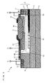
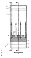
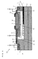
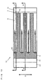
- H10D30/64—Double-diffused metal-oxide semiconductor [DMOS] FETs
- H10D30/65—Lateral DMOS [LDMOS] FETs
-
- H—ELECTRICITY
- H10—SEMICONDUCTOR DEVICES; ELECTRIC SOLID-STATE DEVICES NOT OTHERWISE PROVIDED FOR
- H10D—INORGANIC ELECTRIC SEMICONDUCTOR DEVICES
- H10D12/00—Bipolar devices controlled by the field effect, e.g. insulated-gate bipolar transistors [IGBT]
- H10D12/411—Insulated-gate bipolar transistors [IGBT]
- H10D12/421—Insulated-gate bipolar transistors [IGBT] on insulating layers or insulating substrates, e.g. thin-film IGBTs
-
- H—ELECTRICITY
- H10—SEMICONDUCTOR DEVICES; ELECTRIC SOLID-STATE DEVICES NOT OTHERWISE PROVIDED FOR
- H10D—INORGANIC ELECTRIC SEMICONDUCTOR DEVICES
- H10D30/00—Field-effect transistors [FET]
- H10D30/60—Insulated-gate field-effect transistors [IGFET]
- H10D30/64—Double-diffused metal-oxide semiconductor [DMOS] FETs
- H10D30/65—Lateral DMOS [LDMOS] FETs
- H10D30/657—Lateral DMOS [LDMOS] FETs having substrates comprising insulating layers, e.g. SOI-LDMOS transistors
-
- H—ELECTRICITY
- H10—SEMICONDUCTOR DEVICES; ELECTRIC SOLID-STATE DEVICES NOT OTHERWISE PROVIDED FOR
- H10D—INORGANIC ELECTRIC SEMICONDUCTOR DEVICES
- H10D62/00—Semiconductor bodies, or regions thereof, of devices having potential barriers
- H10D62/10—Shapes, relative sizes or dispositions of the regions of the semiconductor bodies; Shapes of the semiconductor bodies
- H10D62/102—Constructional design considerations for preventing surface leakage or controlling electric field concentration
- H10D62/103—Constructional design considerations for preventing surface leakage or controlling electric field concentration for increasing or controlling the breakdown voltage of reverse-biased devices
- H10D62/105—Constructional design considerations for preventing surface leakage or controlling electric field concentration for increasing or controlling the breakdown voltage of reverse-biased devices by having particular doping profiles, shapes or arrangements of PN junctions; by having supplementary regions, e.g. junction termination extension [JTE]
- H10D62/109—Reduced surface field [RESURF] PN junction structures
- H10D62/111—Multiple RESURF structures, e.g. double RESURF or 3D-RESURF structures
-
- H—ELECTRICITY
- H10—SEMICONDUCTOR DEVICES; ELECTRIC SOLID-STATE DEVICES NOT OTHERWISE PROVIDED FOR
- H10D—INORGANIC ELECTRIC SEMICONDUCTOR DEVICES
- H10D62/00—Semiconductor bodies, or regions thereof, of devices having potential barriers
- H10D62/10—Shapes, relative sizes or dispositions of the regions of the semiconductor bodies; Shapes of the semiconductor bodies
- H10D62/124—Shapes, relative sizes or dispositions of the regions of semiconductor bodies or of junctions between the regions
- H10D62/126—Top-view geometrical layouts of the regions or the junctions
- H10D62/127—Top-view geometrical layouts of the regions or the junctions of cellular field-effect devices, e.g. multicellular DMOS transistors or IGBTs
-
- H—ELECTRICITY
- H10—SEMICONDUCTOR DEVICES; ELECTRIC SOLID-STATE DEVICES NOT OTHERWISE PROVIDED FOR
- H10D—INORGANIC ELECTRIC SEMICONDUCTOR DEVICES
- H10D62/00—Semiconductor bodies, or regions thereof, of devices having potential barriers
- H10D62/10—Shapes, relative sizes or dispositions of the regions of the semiconductor bodies; Shapes of the semiconductor bodies
- H10D62/13—Semiconductor regions connected to electrodes carrying current to be rectified, amplified or switched, e.g. source or drain regions
- H10D62/149—Source or drain regions of field-effect devices
- H10D62/151—Source or drain regions of field-effect devices of IGFETs
- H10D62/156—Drain regions of DMOS transistors
- H10D62/157—Impurity concentrations or distributions
-
- H—ELECTRICITY
- H10—SEMICONDUCTOR DEVICES; ELECTRIC SOLID-STATE DEVICES NOT OTHERWISE PROVIDED FOR
- H10D—INORGANIC ELECTRIC SEMICONDUCTOR DEVICES
- H10D64/00—Electrodes of devices having potential barriers
- H10D64/111—Field plates
-
- H—ELECTRICITY
- H10—SEMICONDUCTOR DEVICES; ELECTRIC SOLID-STATE DEVICES NOT OTHERWISE PROVIDED FOR
- H10D—INORGANIC ELECTRIC SEMICONDUCTOR DEVICES
- H10D64/00—Electrodes of devices having potential barriers
- H10D64/20—Electrodes characterised by their shapes, relative sizes or dispositions
- H10D64/27—Electrodes not carrying the current to be rectified, amplified, oscillated or switched, e.g. gates
- H10D64/311—Gate electrodes for field-effect devices
- H10D64/411—Gate electrodes for field-effect devices for FETs
- H10D64/511—Gate electrodes for field-effect devices for FETs for IGFETs
- H10D64/514—Gate electrodes for field-effect devices for FETs for IGFETs characterised by the insulating layers
- H10D64/516—Gate electrodes for field-effect devices for FETs for IGFETs characterised by the insulating layers the thicknesses being non-uniform
Definitions
- the present invention relates to a semiconductor device, and more specifically to a semiconductor device that is able to prevent deterioration in forward breakdown voltage caused by heat and that facilitates downsizing of the semiconductor device.
- a conventionally known lateral semiconductor device has an SOI (Silicon On Insulator) substrate formed of lamination of a semiconductor substrate, a buried oxide layer, and an active layer, and has a pair of main electrodes formed on the surface of the active layer.
- SOI Silicon On Insulator
- the lateral semiconductor device utilizing the SOI substrate is characteristically less prone to malfunction caused by a surge voltage, and is expected to be a promising semiconductor device.
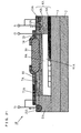
- FIG. 25 schematically shows a cross-sectional view of essential parts of a lateral n-type channel LDMOS (Laterally Diffused MOS) 1000 described in patent literature 1.
- FIG. 26 is a cross-sectional view of the LDMOS shown in FIG. 25 taken along line A-A. It should be noted that electrodes and field oxide layer shown in FIG. 26 are not shown in FIG. 25 .
- the LDMOS 1000 includes a semiconductor substrate 200 made of a single crystal silicon containing a p-type impurity in a high concentration, a buried oxide layer 300 made of silicon oxide (SiO 2 ) and disposed on the semiconductor substrate 200, and an active layer 140 made of a single crystal silicon and disposed on the buried oxide layer 300.
- the active layer 140 includes an n-type well semiconductor region 50, a p-type well semiconductor region 60, a surface semiconductor layer 70, a bottom semiconductor layer 80, an intermediate semiconductor layer 90, and a source semiconductor region 101.
- the n-type well semiconductor region 50 is a semiconductor region surrounding an n-type drain semiconductor region 102.
- the p-type well semiconductor region 60 is a semiconductor region surrounding the n-type source semiconductor region 101.
- the surface semiconductor layer 70 is formed in a part of the top surface of the active layer 140, and is interposed between the n-type well semiconductor region 50 and the p-type well semiconductor region 60. According to the plan view (see FIG. 25 ), the p-type well semiconductor region 60 and the surface semiconductor layer 70 are entirely isolated from each other.
- the surface semiconductor layer 70 contains a p-type impurity (typically boron).
- the surface semiconductor layer 70 is electrically connected to a source terminal S via a contact semiconductor region 70a.
- the bottom semiconductor layer 80 is formed in a part of the bottom surface side of the active layer 140, interposed between the n-type well semiconductor region 50 and the p-type well semiconductor region 60, and isolated by the intermediate semiconductor layer 90 from the surface semiconductor layer 70.
- the bottom semiconductor layer 80 has contact with the n-type well semiconductor region 50, and is isolated from the p-type well semiconductor region 60.
- the bottom semiconductor layer 80 contains an n-type impurity (typically phosphorus). The impurity concentration in the bottom semiconductor layer 80 decreases from its surface joining the buried oxide layer 300 toward its top surface.
- the LDMOS 1000 includes the surface semiconductor layer 70, the intermediate semiconductor layer 90, and the bottom semiconductor layer 80, and accordingly, the critical voltage at an interface between the active layer 140 and the buried oxide layer 300 can be increased, and the breakdown voltage per unit thickness of the buried oxide layer 300 can be improved.
- the surface semiconductor layer 70, the intermediate semiconductor layer 90, and the bottom semiconductor layer 80 form a so-called RESURF (Reduced Surface Field) structure.
- the semiconductor devices described in above patent literature 1 pose the following problems. That is, since the p-type well semiconductor region 60 and the surface semiconductor layer 70 are entirely isolated from each other as viewed in the plan view, current flows in the entire area between the p-type well semiconductor region 60 and the n-type well semiconductor region 50 in the plan view. Thus, in the n-type drain semiconductor region 102, a current amount per unit area increases (causing current crowding), and consequently the n-type drain semiconductor region 102 produces a high-temperature heat. As a result, a problem of deterioration in forward breakdown voltage of LDMOS 1000 has been posed.
- the drain side is set as a high potential side, and thus a large amount of saturation current flows to the drain side. If such a large amount of saturation current flows, the current concentrates at the drain region, of which temperature is rising, and consequently the problem of deterioration in forward breakdown voltage is caused.
- the contact semiconductor region 70a needs to be formed in the surface semiconductor layer 70. With this formation of the contact semiconductor region 70a, the dimensions of the LDMOS 1000 are increased, resulting in a problem of having difficulty in downsizing the LDMOS 1000.
- the present invention has been made in view of the above-described circumstances, and is directed to provide a semiconductor device that is able to prevent deterioration in forward breakdown voltage caused by heat and that facilitates downsizing.
- the present invention adopts the following configuration.
- a first aspect is a lateral semiconductor device, comprising:
- the first aspect of the present invention it is possible to prevent deterioration in breakdown voltage of the semiconductor device.
- downsizing of the semiconductor device can be realized.
- a second aspect of the present invention is a lateral semiconductor device, comprising:
- the second aspect of the present invention it is possible to prevent deterioration in breakdown voltage of the semiconductor device.
- downsizing of the semiconductor device can be realized.
- a third aspect of the present invention is a lateral semiconductor device, comprising:
- the third aspect of the present invention it is possible to prevent deterioration in breakdown voltage of the semiconductor device.
- downsizing of the semiconductor device can be realized.
- the semiconductor device can be downsized.
- a fourth aspect of the present invention is a lateral semiconductor device, comprising:
- the fourth aspect of the present invention it is possible to prevent deterioration in breakdown voltage of the semiconductor device. In addition, downsizing of the semiconductor device can be realized.
- the semiconductor device can be downsized.
- a fifth aspect of the present invention is a lateral semiconductor device, comprising:
- the fifth aspect of the present invention it is possible to prevent deterioration in breakdown voltage of the semiconductor device.
- downsizing of the semiconductor device can be realized.
- the semiconductor device can be downsized.
- a sixth aspect of the present invention is based on any of the third to fifth aspects of the present invention, and characterized in that the part of the second conductivity type surface layer extends along the gate dielectric layer toward the second conductivity type well region.
- the breakdown voltage of the semiconductor device can be further improved.
- a boundary between the second conductivity type surface layer and the second conductivity type well region is further distanced from the drain region or the collector region as compared to a case where a part of the second conductivity type well region extends along the gate dielectric layer to the second conductivity type surface layer (see FIGS. 4 and 6 ). Accordingly, the length of the depletion layer can be increased, and the breakdown voltage of the semiconductor device can be further improved.
- the present invention it is possible to provide a semiconductor device that is able to prevent deterioration in breakdown voltage caused by heat and that facilitates downsizing.
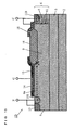
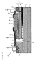
- FIG. 1 is a plan view showing essential parts of a semiconductor device according to a first embodiment of the present invention.
- FIG. 2 is a cross-sectional view of the semiconductor device shown in FIG. 1 taken along line A - A.
- FIG. 3 is a cross-sectional view of the semiconductor device shown in FIG. 1 taken along line B - B. It should be noted that no electrodes or field oxide layer are shown in FIG. 1 .
- first conductivity type and a “second conductivity type” recited in the claims represent an n-type and a p-type, respectively.
- a semiconductor device 1 shown in FIGS. 1 to 3 is a lateral n-type channel LDMOS (Laterally Diffused MOS).
- the semiconductor device 1 includes a semiconductor substrate 2 made of a single crystal silicon containing a second conductivity type (p-type) impurity in a high concentration, a buried oxide layer 3 made of silicon oxide (SiO 2 ) and formed on the semiconductor substrate 2, and an active layer 4 made of a single crystal silicon and formed on the buried oxide layer 3.
- a semiconductor substrate 2 made of a single crystal silicon containing a second conductivity type (p-type) impurity in a high concentration
- a buried oxide layer 3 made of silicon oxide (SiO 2 ) and formed on the semiconductor substrate 2
- an active layer 4 made of a single crystal silicon and formed on the buried oxide layer 3.
- the structure of the active layer 4 is such that a well semiconductor region 6 which is of second conductivity type (p-type) and surrounds a source semiconductor region 10 of first conductivity type (n-type) and a well semiconductor region 5 which is of first conductivity type (n-type) and surrounds a drain semiconductor region 11 of first conductivity type (n-type) are arranged in such a manner as to sandwich a drift region 9 of first conductivity type (n-type).
- a gate electrode 15 is formed via a gate dielectric layer 14 which has contact with a surface of the well semiconductor region 6 of second conductivity type and a surface of the drift region 9 of first conductivity type.
- a surface semiconductor layer 7 of second conductivity type (p-type) which has contact with the gate dielectric layer 14.
- the surface semiconductor layer 7 corresponds to a "second conductivity type surface layer" recited in the claims.
- Parts of the surface semiconductor layer 7 and parts of the well semiconductor region 6 of second conductivity type (p-type) have contact with one another.
- the semiconductor substrate 2 may contain the p-type impurity in a high concentration, or may contain an n-type impurity (typically phosphorus) in a high concentration.
- the semiconductor substrate 2 can substantially be evaluated as a conductive material.
- the resistivity of the semiconductor substrate 2 is preferably set as low as about 1 to 100 m ⁇ cm.
- the thickness of the buried oxide layer 3 is, for example, set to 3 to 5 ⁇ m.
- the active layer 4 has the n-type well semiconductor region 5, the p-type well semiconductor region 6, the surface semiconductor layer 7, a bottom semiconductor layer 8, the drift region 9, and the source semiconductor region 10.
- the thickness of the active layer 4 is, for example, set to about 2.0 to 2.5 ⁇ m. With the thickness of 2.0 ⁇ m or greater, the ESD withstand capability is less likely to deteriorate.
- a known RESURF structure of which application has previously been filed by the applicant of the present invention may be applied (see Japanese laid-open application publication No. 2007 - 173422 ).
- the n-type well semiconductor region 5 is formed as a part of the active layer 4, and contains an n-type impurity (typically phosphorus).
- the impurity concentration in the n-type well semiconductor region 5 is adjusted to approximately 5 ⁇ 10 16 to 5 ⁇ 10 17 cm -3 .
- the n-type well semiconductor region 5 includes in its surface part the drain semiconductor region 11 which contains an n-type impurity (typically phosphorus) in a high concentration.
- the drain semiconductor region 11 can be evaluated as a part of the n-type well semiconductor region 5.
- the impurity concentration in the drain semiconductor region 11 is adjusted to approximately 1 ⁇ 10 19 to 1 ⁇ 10 22 cm -3 .
- the n-type well semiconductor region 5 is electrically connected to a drain terminal D via the drain semiconductor region 11 and a drain electrode (not shown).
- the n-type well semiconductor region 5 extends from the top surface to the bottom surface of the active layer 4.
- the semiconductor device 1 has an overlapped region where a part of the n-type well semiconductor region 5 and a part of the bottom semiconductor layer 8 overlap each other.
- the p-type well semiconductor region 6 is formed as a part of the active layer 4, and is isolated from the n-type well semiconductor region 5 by the drift region 9.
- the p-type well semiconductor region 6 contains a p-type impurity (typically boron).
- the impurity concentration in the p-type well semiconductor region 6 is adjusted to approximately 5 ⁇ 10 16 to 5 ⁇ 10 17 cm -3 .
- the p-type well semiconductor region 6 includes in its surface part a well-contacting semiconductor region 13 which contains a p-type impurity (typically boron) in a high concentration.
- the impurity concentration in the well-contacting semiconductor region 13 is adjusted to approximately 1 ⁇ 10 19 to 1 ⁇ 10 22 cm -3 .
- the well-contacting semiconductor region 13 can be evaluated as a part of the p-type well semiconductor region 6.
- the p-type well semiconductor region 6 is electrically connected to a source electrode S via the well-contacting semiconductor region 13.
- the p-type well semiconductor region 6 extends from the top surface to the bottom surface of the active layer 4.
- the p-type well semiconductor region 6 has contact with the buried oxide layer 3.
- the source semiconductor region 10 is formed in the surface part of the p-type well semiconductor region 6, and is isolated from the drift region 9 by the p-type well semiconductor region 6.
- the source semiconductor region 10 contains an n-type impurity (typically phosphorus) in a high concentration.
- the source semiconductor region 10 is electrically connected to a source terminal S via a source electrode (not shown).
- the surface semiconductor layer 7 is formed in the surface part of the active layer 4, and is interposed between the n-type well semiconductor region 5 and the p-type well semiconductor region 6.
- the surface semiconductor layer 7 contains a p-type impurity (typically boron). The value obtained by integrating the impurity concentrations in the surface semiconductor layer 7 in its thickness direction is adjusted to approximately 1 ⁇ 10 12 to 5 ⁇ 10 12 m -2 .
- the bottom semiconductor layer 8 is formed in the bottom part of the active layer 4, interposed between the n-type well semiconductor region 5 and the p-type well semiconductor region 6, and is isolated from the surface semiconductor layer 7 by the drift region 9.
- the bottom semiconductor layer 8 has contact with the n-type well semiconductor region 5 and is distanced from the p-type well semiconductor region 6.
- the bottom semiconductor layer 8 contains an n-type impurity (typically phosphorus).
- the impurity concentration in the bottom semiconductor layer 8 decreases from its surface joining the buried oxide layer 3 toward its top surface.
- the thickness of the bottom semiconductor layer 8 is adjusted to approximately 0.5 ⁇ m or smaller.
- the bottom semiconductor layer 8 has seven sectional regions. The impurity concentration in the sectional regions varies.
- the impurity concentration in the sectional regions decreases from the one that is proximate to the n-type well semiconductor region 5 toward the one that is proximate to the p-type well semiconductor region 6.
- the impurity concentration in the sectional regions is set higher than the impurity concentration in the drift region 9 interposed between the surface semiconductor layer 7 and the bottom semiconductor layer 8.
- the impurity concentration in the sectional regions increases at integral multiples from the one proximate to the p-type well semiconductor region 6 to the one proximate to the n-type well semiconductor region 5.
- the value obtained by integrating the impurity concentration in the thickness direction is adjusted to approximately 1 ⁇ 10 12 to 5 ⁇ 10 12 cm -2 .
- the drift region 9 is a region in which carriers flow.
- the drift region 9 is in the active layer 4, and has an intermediate region 91 which is interposed between the surface semiconductor layer 7 and the bottom semiconductor layer 8, a first side region 92 which is formed integrally with the intermediate region 91 and positioned closer to the p-type well semiconductor region 6 than the surface semiconductor layer 7 is, and a second side region 93 which is formed integrally with the intermediate region 91 and positioned closer to the n-type well semiconductor region 5 than the surface semiconductor layer 7 is.
- the first side region 92 has contact with the p-type well semiconductor region 6, and the second side region 93 has contact with the n-type well semiconductor region 5.
- the drift region 9 contains an n-type impurity (typically phosphorus) in a low concentration.
- the impurity concentration in the drift region 9, which is interposed between the surface semiconductor layer 7 and the bottom semiconductor layer 8, is set lower than the impurity concentration in the bottom semiconductor layer 8.
- the impurity concentration in the drift region 9 decreases from the bottom surface side toward the top surface side.
- the peak of the impurity concentration in the drift region 9 is located at about its interface with the buried oxide layer 3.
- the value obtained by integrating the impurity concentration in the drift region 9 in the thickness direction is adjusted to approximately 1 ⁇ 10 12 to 5 ⁇ 10 12 cm -2 . Accordingly, the amount of electric charge in the drift region 9 is substantially the same as the amount of electric charge in the surface semiconductor layer 7.
- the semiconductor device 1 includes the gate dielectric layer 14 and the gate electrode 15.
- the gate electrode 15 faces via the gate dielectric layer 14 the p-type well semiconductor region 6 which isolates the source semiconductor region 10 from the drift region 9.
- the gate electrode 15 is electrically connected to the gate terminal S.
- the semiconductor device 1 further includes a field oxide layer 16.
- the field oxide layer 16 is formed in the surface of the active layer 4 in such a manner as to be interposed between the n-type well semiconductor region 5 and the p-type well semiconductor region 6.
- the field oxide layer 16 is formed thicker than the gate dielectric layer 14.
- the planer electrode 18 is electrically connected to the drain electrode D.
- the surface semiconductor layer 7 partially extends along the gate dielectric layer 14 to the p-type well semiconductor region 6. More specifically, as shown in the plan view of FIG. 1 , an end of the surface semiconductor layer 7 that is on the side to the p-type well semiconductor region 6 is formed with alternate projections and depressions. As shown in FIGS. 1 and 3 , an end of the projection (projecting part) 71 has contact with the p-type well semiconductor region 6. As shown in FIGS. 1 and 2 , a depression 72 is distanced from the p-type well semiconductor region 6.
- n-channel region 6a a region directly below the gate dielectric layer 14 where the conductivity type is inverted from p-type to n-type. Since the depressions 72 have no contact with the p-type well semiconductor region 6, a current route is formed in the n-channel region 6a and the first side region 92 of the drift region 9, which are of the same conductivity type (n-type). Along the current route, current flows between the source semiconductor region 10 and the drain semiconductor region 11. That is, carriers present in the source semiconductor region 10 pass through the channel region 6a, the drift region 9 (the first side region 92, the intermediate region 91, and the second side region 93), the n-type well semiconductor region 5, and the drain semiconductor region 11.
- the projections 71 have contact with the p-type well semiconductor region 6, and the conductivity types of the channel region 6a and the surface semiconductor layer 7 are opposite to each other (n-type and p-type, respectively). Accordingly, the current route is interrupted at the contact area, and thus no current flows between the source semiconductor region 10 and the drain semiconductor region 11.
- the contact semiconductor region is unnecessary, and thus the semiconductor device 1 can be downsized. More specifically, since the p-type well semiconductor region 6 and the surface semiconductor layer 7 have contact with each other by means of the projections 71, the source semiconductor region 10 and the surface semiconductor layer 7 have substantially the same electric potential, and thus the contact semiconductor region is unnecessary.
- the dimension of the semiconductor device 1 in the width direction increases.
- the semiconductor device 1 is formed in a ring shape or the like, such increase in dimension of the semiconductor device 1 in the width direction has a smaller impact (substantially no impact) on the size of the semiconductor device 1.
- FIG. 4 is a plan view showing essential parts of a semiconductor device according to a second embodiment of the present invention.
- FIG. 5 is a cross-sectional view of the semiconductor device shown in FIG. 4 taken along line A - A.
- FIG. 5 is a cross-sectional view of the semiconductor device shown in FIG. 1 taken along line B - B. It should be noted that no electrodes or field oxide layer are shown in FIG. 4 .
- components that are identical to those in the first embodiment will be denoted by the corresponding identical reference characters, and no explanation will be given therefor.
- the surface semiconductor layer 7 partially extends along the gate dielectric layer 14 to the p-type well region 6. Meanwhile, in the case of a semiconductor device 1A according to the second embodiment, the p-type well region 6 partially extends along the gate dielectric layer 14 to the surface semiconductor layer 7.
- an end of the p-type well semiconductor region 6 that is on the side to the surface semiconductor layer 7 is formed with alternate projections and depressions.
- an end of the projection (projecting part) 61 has contact with the surface semiconductor layer 7.
- a depression 62 is distanced from the surface semiconductor layer 7.
- the bold line arrow shown in FIG. 4 and the dashed line arrow in FIG. 5 indicate flows of carriers.
- the symbol " X " shown in FIG. 6 indicates no carrier flows.
- the n-channel region 6a (the region directly below the gate dielectric layer 14 where the conductivity type is inverted from p-type to n-type).
- the depressions 62 have no contact with the surface semiconductor layer 7, a current route is formed in the n-channel region 6a and the first side region 92 of the drift region 9, which are of the same conductivity type (n-type).
- current flows between the source semiconductor region 10 and the drain semiconductor region 11. That is, carriers present in the source semiconductor region 10 pass through the channel region 6a, the drift region 9 (the first side region 92, the intermediate region 91, and the second side region 93), the n-type well semiconductor region 5, and the drain semiconductor region 11.
- the projections 61 have contact with the surface semiconductor layer 7, and the conductivity types of the channel region 6a and the surface semiconductor layer 7 are opposite to each other (n-type and p-type, respectively). Accordingly, the current route is interrupted at the contact area, and thus no current flows between the source semiconductor region 10 and the drain semiconductor region 11.
- a current amount per unit area of the semiconductor device 1A can be reduced.
- the reduction in current amount per unit area enables prevention of current crowding from occurring in the drain semiconductor region 11 as well as prevention of deterioration in forward breakdown voltage of the semiconductor device 1A.
- a contact semiconductor region needs to be formed in the surface semiconductor layer.
- the contact semiconductor region is unnecessary, and thus the semiconductor device 1 can be downsized. More specifically, since the p-type well semiconductor region 6 and the surface semiconductor layer 7 have contact with each other by means of the projections 61, the source semiconductor region 10 and the surface semiconductor layer 7 have substantially the same electric potential, and thus the contact semiconductor region is unnecessary.
- FIG. 7 is a plan view showing essential parts of a semiconductor device according to a third embodiment of the present invention.
- FIG. 8 is a cross-sectional view of the semiconductor device shown in FIG. 7 taken along line A - A.
- FIG. 9 is a cross-sectional view of the semiconductor device shown in FIG. 7 taken along line B - B. It should be noted that no electrodes or field oxide layer are shown in FIG. 7 .
- components that are identical to those in the first embodiment will be denoted by the corresponding identical reference characters, and no explanation will be given therefor.
- the above-described first embodiment is an embodiment on the lateral n-type channel LDMOS, whereas the third embodiment is an embodiment on a lateral n-type channel LIGBT (lateral insulated gate bipolar transistor).
- LIGBT lateral insulated gate bipolar transistor
- a semiconductor device 1B according to the third embodiment includes a collector semiconductor region 110 containing a p-type impurity (typically boron) in a high concentration, which corresponds to the drain semiconductor region 11 containing an n-type impurity in a high concentration according to the first embodiment.
- the collector semiconductor region 110 is electrically connected to a collector terminal C via a collector electrode (not shown).
- the region which functions as the source semiconductor region 10 in the first embodiment is replaced with an emitter semiconductor region 100 in the present embodiment.
- the emitter semiconductor region 100 is electrically connected to an emitter terminal E via an emitter electrode (not shown).
- the surface semiconductor layer 7 partially extends along the gate dielectric layer 14 to the p-type well semiconductor region 6. More specifically, as shown in the plan view of FIG. 7 , an end of the surface semiconductor layer 7 that is on the side to the p-type well semiconductor region 6 is formed with alternate projections and depressions. As shown in FIGS. 7 and 9 , an end of the projection (projecting part) 71 has contact with the p-type well semiconductor region 6. As shown in FIGS. 7 and 8 , the depression 72 is distanced from the p-type well semiconductor region 6.
- the n-channel region 6a (the region directly below the gate dielectric layer 14 where the conductivity type is inverted from p-type to n-type).
- the depressions 72 have no contact with the p-type well semiconductor region 6, a current route is formed in the n-channel region 6a and the first side region 92 of the drift region 9, which are of the same conductivity type (n-type).
- current flows between the emitter semiconductor region 100 and the collector semiconductor region 110. That is, carriers present in the emitter semiconductor region 100 pass through the channel region 6a, the drift region 9 (the first side region 92, the intermediate region 91, and the second side region 93), the n-type well semiconductor region 5, and the collector semiconductor region 110.
- the projections 71 have contact with the p-type well semiconductor region 6, and the conductivity types of the channel region 6a and the surface semiconductor layer 7 are opposite to each other (n-type and p-type, respectively). Accordingly, the current route is interrupted at the contact area, and thus no current flows between the emitter semiconductor region 100 and the collector semiconductor region 110.
- a current amount per unit area of the semiconductor device 1B can be reduced.
- the reduction in current amount per unit area enables prevention of current crowding from occurring in the collector semiconductor region 110 as well as prevention of deterioration in forward breakdown voltage of the semiconductor device 1B.
- the contact semiconductor region is unnecessary, and thus the semiconductor device 1B can be downsized. More specifically, since the p-type well semiconductor region 6 and the surface semiconductor layer 7 have contact with each other by means of the projections 71, the source semiconductor region 10 and the surface semiconductor layer 7 have substantially the same electric potential, and thus the contact semiconductor region is unnecessary.
- the dimension of the semiconductor device 1B in the width direction increases.
- the semiconductor device 1B is formed in a ring shape or the like, such increase in dimension of the semiconductor device 1B in the width direction has a smaller impact (substantially no impact) on the size of the semiconductor device 1B.
- FIG. 10 is a plan view showing essential parts of a semiconductor device according to a fourth embodiment of the present invention.
- FIG. 11 is a cross-sectional view of the semiconductor device shown in FIG. 10 taken along line A - A.
- FIG. 12 is a cross-sectional view of the semiconductor device shown in FIG. 10 taken along line B - B. It should be noted that no electrodes or field oxide layer are shown in FIG. 10 .
- components that are identical to those in the first embodiment will be denoted by the corresponding identical reference characters, and no explanation will be given therefor.
- a semiconductor device 1C according to the fourth embodiment does not include the surface semiconductor layer 7 or the bottom semiconductor layer 8 which are included in the device according to the first embodiment.
- the following structure is adopted.
- the drift region 9 is not divided into the intermediate region, the first side region, or the second side region unlike the first embodiment.
- the drift region 9 has contact with the p-type well semiconductor region 6 at its one end and with the n-type well semiconductor region 5 at the other end.
- the p-type well semiconductor region 6 partially extends along the gate dielectric layer 14 in the n-type drift region 9. Specifically, the p-type well semiconductor region 6 partially extends, in the drift region 9, longer than the length of the gate dielectric layer 14 in a direction in which carriers move (i.e., to the position beyond the part directly below the boundary between the gate dielectric layer 14 and the field oxide layer 16).
- an end of the p-type well semiconductor region 6 that is on the side to the n-type well semiconductor region 5 is formed with alternate projections and depressions.
- an end of the projection (projecting part) 61 has contact with the n-type well semiconductor region 5.
- the depression 62 is distanced from the n-type well semiconductor region 5, and does not reach the position directly below the boundary between the gate dielectric layer 14 and the field oxide layer 16.
- the n-channel region 6a (the region directly below the gate dielectric layer 14 where the conductivity type is inverted from p-type to n-type).
- the depressions 62 are shorter in the direction in which carriers move than the gate dielectric layer 14 (i.e., not extending beyond the gate dielectric layer 14)
- a current route is formed in the n-channel region 6a and the drift region 9, which are of the same conductivity type (n-type).
- current flows between the source semiconductor region 10 and the drain semiconductor region 11. That is, carriers present in the source semiconductor region 10 pass through the channel region 6a, the drift region 9, the n-type well semiconductor region 5, and the drain semiconductor region 11.
- the projections 61 extend longer than the length of the gate dielectric layer 14 in the direction in which carriers move (i.e., to the position beyond the gate dielectric layer 14 (the position reaching the n-type well semiconductor region 5 in FIG. 12 )). Accordingly, the current route is interrupted in the projections 61 at the part directly below the boundary between the gate dielectric layer 14 and the field oxide layer 16, and thus no current flows between the source semiconductor region 10 and the drain semiconductor region 11.
- a current amount per unit area of the semiconductor device 1C can be reduced.
- the reduction in current amount per unit area enables prevention of current crowding from occurring in the drain semiconductor region 11 as well as prevention of deterioration in forward breakdown voltage of the semiconductor device 1C.
- the above-described fourth embodiment may have a structure in which the n-type and the p-type are reversed.
- FIG. 13 is a plan view showing essential parts of a semiconductor device according to a fifth embodiment of the present invention.
- FIG. 14 is a cross-sectional view of the semiconductor device shown in FIG. 13 taken along line A - A.
- FIG. 15 is a cross-sectional view of the semiconductor device shown in FIG. 13 taken along line B - B. It should be noted that no electrodes or field oxide layer are shown in FIG. 13 .
- components that are identical to those in the fourth embodiment will be denoted by the corresponding identical reference characters, and no explanation will be given therefor.
- the above-described fourth embodiment is an embodiment on the lateral n-type channel LDMOS, whereas the fifth embodiment is an embodiment on a lateral n-type channel LIGBT (lateral insulated gate bipolar transistor).
- LIGBT lateral insulated gate bipolar transistor
- a semiconductor device 1D according to the fifth embodiment includes a collector semiconductor region 110 containing a p-type impurity (typically boron) in a high concentration, which corresponds to the drain semiconductor region 11 containing an n-type impurity in a high concentration according to the fourth embodiment.
- the collector semiconductor region 110 is electrically connected to a collector terminal C via the collector electrode (not shown).
- the region which functions as the source semiconductor region 10 in the fourth embodiment is replaced with an emitter semiconductor region 100 in the fifth embodiment.
- the emitter semiconductor region 100 is electrically connected to the emitter terminal E via an emitter electrode (not shown).
- the structure having projections and depressions similar to that in the fourth embodiment is adopted.
- an end of the p-type well semiconductor region 6 that is on the side to the n-type well semiconductor region 5 is formed with alternate projections and depressions.
- an end of the projection (projecting part) 61 has contact with the n-type well semiconductor region 5.
- the depression 62 is distanced from the n-type well semiconductor region 5, and does not reach the part directly below the boundary between the gate dielectric layer 14 and the field oxide layer 16.
- parts where current flows and parts where no current flows are formed alternately in the semiconductor device 1D in the width direction (Y direction as shown in FIG. 13 ), and consequently, a current amount per unit area of the semiconductor device 1D can be reduced.
- the reduction in current amount per unit area enables prevention of current crowding from occurring in the drain semiconductor region 11 as well as prevention of deterioration in forward breakdown voltage of the semiconductor device 1D.
- the semiconductor device 1D can be downsized.
- FIG. 16 is a plan view showing essential parts of a semiconductor device according to a sixth embodiment of the present invention.
- FIG. 17 is a cross-sectional view of the semiconductor device shown in FIG. 16 taken along line A - A.
- FIG. 18 is a cross-sectional view of the semiconductor device shown in FIG. 16 taken along line B - B. It should be noted that no electrodes or field oxide layer are shown in FIG. 16 .
- components that are identical to those in the first embodiment will be denoted by the corresponding identical reference characters, and no explanation will be given therefor.
- a semiconductor device 1E according to the sixth embodiment is different from that according to the first embodiment in that a bottom semiconductor layer 17 is formed between the surface semiconductor layer 7 and the bottom semiconductor layer 8.
- the semiconductor active layer 4 includes the bottom semiconductor layer 17 instead of the intermediate region 91 of the drift region 9 according to the first embodiment.
- the bottom semiconductor layer 17 has contact at its one end with the n-type well semiconductor region 5.
- the bottom semiconductor layer 17 contains an n-type impurity (typically phosphorus).
- the impurity concentration is higher than the impurity concentration in the intermediate region 91 of the drift region 9 according to the first embodiment.
- FIG. 19 is a plan view showing essential parts of a semiconductor device according to a seventh embodiment of the present invention.
- FIG. 20 is a cross-sectional view of the semiconductor device shown in FIG. 19 taken along line A - A.
- FIG. 21 is a cross-sectional view of the semiconductor device shown in FIG. 19 taken along line B - B. It should be noted that no electrodes or field oxide layer are shown in FIG. 19 .
- components that are identical to those in the first embodiment will be denoted by the corresponding identical reference characters, and no explanation will be given therefor.
- the above-described first embodiment is an embodiment on the lateral n-type channel LDMOS, whereas the seventh embodiment will be an embodiment on a p-type channel LDMOS.
- the semiconductor device 1F includes the semiconductor substrate 2 made of a single crystal silicon containing a second conductivity type (p-type) impurity in a high concentration, the buried oxide layer 3 made of silicon oxide (SiO 2 ) formed on the semiconductor substrate 2, and the active layer 4A made of a single crystal silicon formed on the buried oxide layer 3.
- the semiconductor substrate 2 made of a single crystal silicon containing a second conductivity type (p-type) impurity in a high concentration
- the buried oxide layer 3 made of silicon oxide (SiO 2 ) formed on the semiconductor substrate 2
- the active layer 4A made of a single crystal silicon formed on the buried oxide layer 3.
- the structure of the active layer 4 is such that a well semiconductor region 6A which is of first conductivity type (n-type) and surrounds a source semiconductor region 10A of second conductivity type (p-type) and a well semiconductor region 5A which is of second conductivity type (p-type) and surrounds a drain semiconductor region 11A of second conductivity type (p-type) are arranged in such a manner as to sandwich a drift region 9A of first conductivity type (n-type).
- the gate electrode 15 is formed via the gate dielectric layer 14 which has contact with the surface of the well semiconductor region 6A of first conductivity type and with the surface of the drift region 9A of first conductivity type.
- a surface semiconductor layer 7A of second conductivity type (p-type) which has contact with the gate dielectric layer 14.
- the surface semiconductor layer 7A corresponds to the " second conductivity type surface layer" recited in the claims.
- Parts of the surface semiconductor layer 7 and parts of the well semiconductor region 5A of second conductivity type (p-type) are connected with one another.
- the semiconductor substrate 2 may contain the p-type impurity in a high concentration, or may contain an n-type impurity (typically phosphorus) in a high concentration.
- the semiconductor substrate 2 can substantially be evaluated as a conductive material.
- the resistivity of the semiconductor substrate 2 is preferably set as low as about 1 to 100 m ⁇ cm.
- the thickness of the buried oxide layer 3 is, for example, set to 3 to 5 ⁇ m
- the active layer 4A has the p-type well semiconductor region 5A, the n-type well semiconductor region 6A, the surface semiconductor layer 7A, a bottom semiconductor layer 8A, the drift region 9A, and the source semiconductor region 10A.
- the thickness of the active layer 4A is, for example, set to about 2.0 to 2.5 ⁇ m. With the thickness of 2.0 ⁇ m or greater, the ESD withstand capability is less likely to deteriorate.
- a known RESURF structure of which application has previously been filed by the applicant of the present invention may be applied (see Japanese laid-open application publication No. 2007 - 173422 ).
- the p-type well semiconductor region 5A is formed as a part of the active layer 4A, and contains a p-type impurity (typically boron).
- the impurity concentration in the p-type well semiconductor region 5A is adjusted to approximately 5 ⁇ 10 16 to 5 ⁇ 10 17 cm -3 .
- the p-type well semiconductor region 5A includes in its surface part the drain semiconductor region 11A which contains a p-type impurity (typically boron) in a high concentration.
- the drain semiconductor region 11A can be evaluated as a part of the p-type well semiconductor region 5A.
- the impurity concentration in the drain semiconductor region 11A is adjusted to approximately 1 ⁇ 10 19 to 1 ⁇ 10 22 cm -3 .
- the p-type well semiconductor region 5A is electrically connected to the drain terminal D via the drain semiconductor region 11A and the drain electrode (not shown).
- the p-type well semiconductor region 5A extends from the top surface to the bottom surface of the active layer 4A.
- the semiconductor device 1F has an overlapped region where a part of the p-type well semiconductor region 5A and a part of the bottom semiconductor layer 8A overlap each other.
- the n-type well semiconductor region 6A is formed as a part of the active layer 4A, and is isolated from the p-type well semiconductor region 5A by the drift region 9A.
- the n-type well semiconductor region 6A contains an n-type impurity (typically phosphorus).
- the impurity concentration in the n-type well semiconductor region 6A is adjusted to approximately 5 ⁇ 10 16 to 5 ⁇ 10 17 cm -3 .
- the n-type well semiconductor region 6A includes in its surface part a well-contacting semiconductor region 13A which contains an n-type impurity (typically phosphorus) in a high concentration.
- the impurity concentration in the well-contacting semiconductor region 13A is adjusted to approximately 1 ⁇ 10 19 to 1 ⁇ 10 22 cm -3 .
- the well-contacting semiconductor region 13A can be evaluated as a part of the n-type well semiconductor region 6A.
- the n-type well semiconductor region 6A is electrically connected to the source terminal S via the well-contacting semiconductor region 13A and the source electrode (not shown).
- the n-type well semiconductor region 6A extends from the top surface to the bottom surface of the active layer 4A.
- the n-type well semiconductor region 6A has contact with the buried oxide layer 3.
- the source semiconductor region 10A is formed in the surface part of the n-type well semiconductor region 6A, and is isolated from the drift region 9A by the n-type well semiconductor region 6.
- the source semiconductor region 10A contains a p-type impurity (typically boron) in a high concentration.
- the source semiconductor region 10A is electrically connected to the source terminal S via the source electrode (not shown).
- the surface semiconductor layer 7A is formed in the surface part of the active layer 4A, and is interposed between the p-type well semiconductor region 5A and the n-type well semiconductor region 6A.
- the surface semiconductor layer 7A contains a p-type impurity (typically boron). The value obtained by integrating the impurity concentrations in the surface semiconductor layer 7A in its thickness direction is adjusted to approximately 1 ⁇ 10 12 to 5 ⁇ 10 12 cm -2 . An end of the surface semiconductor layer 7 has contact with the n-type well semiconductor region 6A.
- the bottom semiconductor layer 8A is formed in the bottom part of the active layer 4A, interposed between the p-type well semiconductor region 5A and the n-type well semiconductor region 6A, and isolated from the surface semiconductor layer 7A by the drift region 9A.
- the bottom semiconductor layer 8A has contact with the n-type well semiconductor region 6A and is distanced from the n-type well semiconductor region 5A.
- the bottom semiconductor layer 8A contains an n-type impurity (typically phosphorus).
- the impurity concentration in the bottom semiconductor layer 8A decreases from its surface joining the buried oxide layer 3 toward its top surface.
- the thickness of the bottom semiconductor layer 8A is adjusted to approximately 0.5 ⁇ m or smaller.
- the bottom semiconductor layer 8A has seven sectional regions. The impurity concentration in the sectional regions varies.
- the impurity concentration in the sectional regions decreases from the one that is proximate to the n-type well semiconductor region 6A toward the one that is proximate to the p-type well semiconductor region 5A.
- the impurity concentration in the sectional regions is set higher than the impurity concentration in the drift region 9A interposed between the surface semiconductor layer 7A and the bottom semiconductor layer 8A.
- the impurity concentration in the sectional regions increases at integral multiples from the one proximate to the p-type well semiconductor region 5A to the one proximate to the n-type well semiconductor region 6A.
- the value obtained by integrating the impurity concentration in the thickness direction is adjusted to approximately 1 ⁇ 10 12 to 5 ⁇ 10 12 cm -2 .
- the drift region 9A is a region in which carriers flow.
- the drift region 9A is in the active layer 4A, and has a main area 91A which is interposed between the surface semiconductor layer 7A and the bottom semiconductor layer 8A, and a first side region 92A which is formed integrally with the main area 91A and positioned closer to the p-type well semiconductor region 5A than the surface semiconductor layer 7A is.
- the main area 91A has contact with the n-type well semiconductor region 6A, and the first side region 92A has contact with the p-type well semiconductor region 5A.
- the drift region 9A contains an n-type impurity (typically phosphorus) in a low concentration.
- the impurity concentration in the drift region 9A which is interposed between the surface semiconductor layer 7A and the bottom semiconductor layer 8A, is set lower than the impurity concentration in the bottom semiconductor layer 8A.
- the impurity concentration in the drift region 9A decreases from the bottom surface side toward the top surface side.
- the peak of the impurity concentration in the drift region 9A is located at about its interface with the buried oxide layer 3.
- the value obtained by integrating the impurity concentration in the drift region 9A in the thickness direction is adjusted to approximately 1 ⁇ 10 12 to 5 ⁇ 10 12 cm -2 . Accordingly, the amount of electric charge in the drift region 9A is substantially the same as the amount of electric charge in the surface semiconductor layer 7A.
- the semiconductor device 1F includes the gate dielectric layer 14 and the gate electrode 15.
- the gate electrode 15 faces via the gate dielectric layer 14 the n-type well semiconductor region 6A which isolates the source semiconductor region 10A from the drift region 9A.
- the gate electrode 15 is electrically connected to the gate terminal S.
- the semiconductor device 1F further includes the field oxide layer 16.
- the field oxide layer 16 is formed in the surface of the active layer 4A in such a manner as to be interposed between the n-type well semiconductor region 6A and the p-type well semiconductor region 5A.
- the planer electrode 18 is electrically connected to the drain electrode D.
- the surface semiconductor layer 7A partially extends along the gate dielectric layer 14 to the p-type well semiconductor region 5A. More specifically, as shown in the plan view of FIG. 19 , an end of the surface semiconductor layer 7A that is on the side to the p-type well semiconductor region 5A is formed with alternate projections and depressions. As shown in FIGS. 19 and 21 , an end of a projection (projecting part) 71A has contact with the p-type well semiconductor region 5A. As shown in FIGS. 19 and 20 , a depression 72A is distanced from the p-type well semiconductor region 5A.
- a p-channel region 60a (a region directly below the gate dielectric layer 14 where the conductivity type is inverted from n-type to p-type).
- a current route is formed in the p-channel region 60a and the surface semiconductor layer 7A, which are of the same conductivity type (p-type), and a current flows through the current route between the source semiconductor region 10A and the drain semiconductor region 11A. That is, carriers present in the source semiconductor region 10A pass through the channel region 60a, the surface semiconductor layer 7A, the p-type well semiconductor region 5A, and the drain semiconductor region 11A.
- the depressions 72A have no contact with the p-type well semiconductor region 5A, but have contact with the first side region 92A. Since the conductivity types of the surface semiconductor layer 7A and the first side region 92A are opposite to each other (p-type and n-type, respectively), the current route is interrupted at the contact area between the surface semiconductor layer 7A and the first side region 92A, and thus no current flows between the source semiconductor region 10A and the drain semiconductor region 11A.
- a current amount per unit area of the semiconductor device 1F can be reduced.
- the reduction in the current amount per unit area enables prevention of current crowding from occurring in the drain semiconductor region 11A as well as prevention of deterioration in forward breakdown voltage of the semiconductor device 1F.
- the contact semiconductor region is unnecessary, and thus the semiconductor device 1F can be downsized. More specifically, since the p-type well semiconductor region 5A and the surface semiconductor layer 7A have contact with each other by means of the projections 71A, the drain semiconductor region 11A and the surface semiconductor layer 7A have substantially the same electric potential, and thus there is no need to arrange a contact semiconductor region for causing the surface semiconductor layer 7A and the drain semiconductor region 11A to have the same electric potential.
- FIG. 22 is a plan view showing essential parts of a semiconductor device according to an eighth embodiment of the present invention.
- FIG. 23 is a cross-sectional view of the semiconductor device shown in FIG. 22 taken along line A - A.
- FIG. 24 is a cross-sectional view of the semiconductor device shown in FIG. 22 taken along line B - B. It should be noted that no electrodes or field oxide layer are shown in FIG. 22 .
- components that are identical to those in the seventh embodiment will be denoted by the corresponding identical reference characters, and no explanation will be given therefor.
- a semiconductor device 1G according to the eighth embodiment is different from that according to the seventh embodiment in that a bottom semiconductor layer 17 is formed between the surface semiconductor layer 7A and the bottom semiconductor layer 8A.
- the active layer 4A includes the bottom semiconductor layer 17 instead of the main area 91A of the drift region 9A according to the seventh embodiment.
- the bottom semiconductor layer 17 has contact at its one end with the n-type well semiconductor region 6A.
- the bottom semiconductor layer 17 contains an n-type impurity (typically phosphorus).
- the impurity concentration is higher than the impurity concentration in the main area 91A of the drift region 9A described in the seventh embodiment.
- the present invention is applicable to a semiconductor device or the like which is able to prevent deterioration in breakdown voltage caused by heat and which facilitates downsizing.
Landscapes
- Thin Film Transistor (AREA)
- Insulated Gate Type Field-Effect Transistor (AREA)
- Chemical & Material Sciences (AREA)
- Composite Materials (AREA)
Abstract
Description
- The present invention relates to a semiconductor device, and more specifically to a semiconductor device that is able to prevent deterioration in forward breakdown voltage caused by heat and that facilitates downsizing of the semiconductor device.
- A conventionally known lateral semiconductor device has an SOI (Silicon On Insulator) substrate formed of lamination of a semiconductor substrate, a buried oxide layer, and an active layer, and has a pair of main electrodes formed on the surface of the active layer. The lateral semiconductor device utilizing the SOI substrate is characteristically less prone to malfunction caused by a surge voltage, and is expected to be a promising semiconductor device.
- An example of the above-described semiconductor device is disclosed by
patent literature 1.FIG. 25 schematically shows a cross-sectional view of essential parts of a lateral n-type channel LDMOS (Laterally Diffused MOS) 1000 described inpatent literature 1.FIG. 26 is a cross-sectional view of the LDMOS shown inFIG. 25 taken along line A-A. It should be noted that electrodes and field oxide layer shown inFIG. 26 are not shown inFIG. 25 . - The LDMOS 1000 includes a
semiconductor substrate 200 made of a single crystal silicon containing a p-type impurity in a high concentration, a buriedoxide layer 300 made of silicon oxide (SiO2) and disposed on thesemiconductor substrate 200, and anactive layer 140 made of a single crystal silicon and disposed on the buriedoxide layer 300. - The
active layer 140 includes an n-typewell semiconductor region 50, a p-typewell semiconductor region 60, asurface semiconductor layer 70, abottom semiconductor layer 80, anintermediate semiconductor layer 90, and asource semiconductor region 101. - The n-type
well semiconductor region 50 is a semiconductor region surrounding an n-typedrain semiconductor region 102. The p-typewell semiconductor region 60 is a semiconductor region surrounding the n-typesource semiconductor region 101. - The
surface semiconductor layer 70 is formed in a part of the top surface of theactive layer 140, and is interposed between the n-typewell semiconductor region 50 and the p-typewell semiconductor region 60. According to the plan view (seeFIG. 25 ), the p-typewell semiconductor region 60 and thesurface semiconductor layer 70 are entirely isolated from each other. Thesurface semiconductor layer 70 contains a p-type impurity (typically boron). Thesurface semiconductor layer 70 is electrically connected to a source terminal S via acontact semiconductor region 70a. - The
bottom semiconductor layer 80 is formed in a part of the bottom surface side of theactive layer 140, interposed between the n-typewell semiconductor region 50 and the p-typewell semiconductor region 60, and isolated by theintermediate semiconductor layer 90 from thesurface semiconductor layer 70. Thebottom semiconductor layer 80 has contact with the n-typewell semiconductor region 50, and is isolated from the p-typewell semiconductor region 60. Thebottom semiconductor layer 80 contains an n-type impurity (typically phosphorus). The impurity concentration in thebottom semiconductor layer 80 decreases from its surface joining the buriedoxide layer 300 toward its top surface. - The LDMOS 1000 includes the
surface semiconductor layer 70, theintermediate semiconductor layer 90, and thebottom semiconductor layer 80, and accordingly, the critical voltage at an interface between theactive layer 140 and the buriedoxide layer 300 can be increased, and the breakdown voltage per unit thickness of the buriedoxide layer 300 can be improved. Thesurface semiconductor layer 70, theintermediate semiconductor layer 90, and thebottom semiconductor layer 80 form a so-called RESURF (Reduced Surface Field) structure. - However, the semiconductor devices described in
above patent literature 1 pose the following problems. That is, since the p-typewell semiconductor region 60 and thesurface semiconductor layer 70 are entirely isolated from each other as viewed in the plan view, current flows in the entire area between the p-typewell semiconductor region 60 and the n-typewell semiconductor region 50 in the plan view. Thus, in the n-typedrain semiconductor region 102, a current amount per unit area increases (causing current crowding), and consequently the n-typedrain semiconductor region 102 produces a high-temperature heat. As a result, a problem of deterioration in forward breakdown voltage ofLDMOS 1000 has been posed. In particular, in the case of designing the LDMOS 1000 as a level-shifting device, the drain side is set as a high potential side, and thus a large amount of saturation current flows to the drain side. If such a large amount of saturation current flows, the current concentrates at the drain region, of which temperature is rising, and consequently the problem of deterioration in forward breakdown voltage is caused. - In addition, in order to set the
surface semiconductor layer 70 and thesource semiconductor region 101 to have the same electric potential, thecontact semiconductor region 70a needs to be formed in thesurface semiconductor layer 70. With this formation of thecontact semiconductor region 70a, the dimensions of theLDMOS 1000 are increased, resulting in a problem of having difficulty in downsizing theLDMOS 1000. - [PTL 1] Japanese laid-open application publication No.
2007-173422 - The present invention has been made in view of the above-described circumstances, and is directed to provide a semiconductor device that is able to prevent deterioration in forward breakdown voltage caused by heat and that facilitates downsizing.
- In order to solve the above-described problems, the present invention adopts the following configuration.
- A first aspect is a lateral semiconductor device, comprising:
- a semiconductor substrate;
- a buried oxide layer formed on the semiconductor substrate; and
- an active layer formed on the buried oxide layer,
- the active layer comprising:
- a second conductivity type well region surrounding a first conductivity type source region;
- a first conductivity type well region surrounding a first conductivity type drain region;
- a first conductivity type drift region interposed between the second conductivity type well region and the first conductivity type well region; and
- a gate electrode formed in a part of a surface of the active layer via a gate dielectric layer which has contact with a surface of the second conductivity type well region and a surface of the first conductivity type drift region, wherein
- the second conductivity type well region partially extends along the gate dielectric layer, longer in a direction in which carriers move than a length of the gate dielectric layer, into the first conductivity type drift region.
- According to the first aspect of the present invention, it is possible to prevent deterioration in breakdown voltage of the semiconductor device. In addition, downsizing of the semiconductor device can be realized.
- More specifically, no carrier flows from the first conductivity type source region to the first conductivity type drain region through a part where the second conductivity type well region extends (see
FIGS. 10 and12 ), whereas carriers flow from the first conductivity type source region to the first conductivity type drain region through a part where the second conductivity type well region does not extend (seeFIGS. 10 and11 ). Accordingly, a part where current flows and a part where no current flows are formed between the first conductivity type source region and the first conductivity type drain region, and consequently, a current amount per unit area of the first conductivity type drain region can be reduced. Accordingly, a heating value per unit area of the first conductivity type drain region can be reduced, and it is possible to prevent the temperature of the first conductivity type drain region from rising excessively. And it is also possible to prevent deterioration in breakdown voltage of the semiconductor device. - Further, since no surface semiconductor layer is provided, it is unnecessary to form a contact semiconductor region in the surface semiconductor layer, and thus the semiconductor device can be downsized.
- A second aspect of the present invention is a lateral semiconductor device, comprising:
- a semiconductor substrate;
- a buried oxide layer formed on the semiconductor substrate; and
- an active layer formed on the buried oxide layer,
- the active layer comprising:
- a second conductivity type well region surrounding a first conductivity type emitter region;
- a first conductivity type well region surrounding a second conductivity type collector region;
- a first conductivity type drift region interposed between the second conductivity type well region and the first conductivity type well region; and
- a gate electrode formed in a part of a surface of the active layer via a gate dielectric layer which has contact with a surface of the second conductivity type well region and a surface of the first conductivity type drift region, wherein
- the second conductivity type well region partially extends along the gate dielectric layer, longer in a direction in which carriers move than a length of the gate dielectric layer, into the first conductivity type drift region.
- According to the second aspect of the present invention, it is possible to prevent deterioration in breakdown voltage of the semiconductor device. In addition, downsizing of the semiconductor device can be realized.
- More specifically, no carrier flows from the first conductivity type emitter region to the second conductivity type collector region through a part where the second conductivity type well region extends (see
FIGS. 13 and15 ), whereas carriers flow from the first conductivity type emitter region to the second conductivity type collector region through a part where the second conductivity type well region does not extend (seeFIGS. 13 and14 ). Accordingly, a part where current flows and a part where no current flows are formed between the first conductivity type emitter region and the second conductivity type collector region, and consequently, a current amount per unit area of the second conductivity type collector region can be reduced. Accordingly, a heating value per unit area of the second conductivity type collector region can be reduced, and it is possible to prevent the temperature of the second conductivity type collector region from rising excessively. And it is also possible to prevent deterioration in breakdown voltage of the semiconductor device. - Further, since no surface semiconductor layer is provided, it is unnecessary to form a contact semiconductor region in the surface semiconductor layer, and thus the semiconductor device can be downsized.
- A third aspect of the present invention is a lateral semiconductor device, comprising:
- a semiconductor substrate;
- a buried oxide layer formed on the semiconductor substrate; and
- an active layer formed on the buried oxide layer,
- the active layer comprising:
- a second conductivity type well region surrounding a first conductivity type source region;
- a first conductivity type well region surrounding a first conductivity type drain region;
- a first conductivity type drift region interposed between the second conductivity type well region and the first conductivity type well region; and
- a gate electrode formed in a part of a surface of the active layer via a gate dielectric layer which has contact with a surface of the second conductivity type well region and a surface of the first conductivity type drift region, wherein
- in a surface part of the first conductivity type drift region, a second conductivity type surface layer having contact with the gate dielectric layer is laminated, and
- a part of the second conductivity type surface layer and a part of the second conductivity type well region have contact with each other.
- According to the third aspect of the present invention, it is possible to prevent deterioration in breakdown voltage of the semiconductor device. In addition, downsizing of the semiconductor device can be realized.
- More specifically, no carrier flows from the first conductivity type source region to the first conductivity type drain region through a part where the second conductivity type surface layer has contact with the second conductivity type well region (see
FIG. 1 and3 ), whereas carriers flow from the first conductivity type source region to the first conductivity type drain region through a part where the second conductivity type surface layer has no contact with the second conductivity type well region (seeFIG. 1 and2 ). Accordingly, a part where current flows and a part where no current flows are formed between the first conductivity type source region and the first conductivity type drain region, and consequently, a current amount per unit area of the first conductivity type drain region can be reduced. Accordingly, a heating value per unit area of the first conductivity type drain region can be reduced, and it is possible to prevent the temperature of the first conductivity type drain region from rising excessively. And it is possible to prevent deterioration in breakdown voltage of the semiconductor device. - Further, since a part of the second conductivity type surface layer and a part of the second conductivity type well region have contact with each other, the second conductivity type surface layer and the first conductivity type source region have the same electric potential without having a contact semiconductor region in the surface semiconductor layer, and thus, the semiconductor device can be downsized.
- A fourth aspect of the present invention is a lateral semiconductor device, comprising:
- a semiconductor substrate;
- a buried oxide layer formed on the semiconductor substrate; and
- an active layer formed on the buried oxide layer,
- the active layer comprising:
- a second conductivity type well region surrounding a first conductivity type emitter region;
- a first conductivity type well region surrounding a second conductivity type collector region;
- a first conductivity type drift region interposed between the second conductivity type well region and the first conductivity type well region; and
- a gate electrode formed in a part of a surface of the active layer via a gate dielectric layer which has contact with a surface of the second conductivity type well region and a surface of the first conductivity type drift region; wherein
- in a surface part of the first conductivity type drift region, a second conductivity type surface layer having contact with the gate dielectric layer is formed, and
- a part of the second conductivity type surface layer and a part of the second conductivity type well region have contact with each other.
- According to the fourth aspect of the present invention, it is possible to prevent deterioration in breakdown voltage of the semiconductor device. In addition, downsizing of the semiconductor device can be realized.
- More specifically, no carrier flows from the first conductivity type emitter region to the second conductivity type collector region through a part where the second conductivity type surface layer has contact with the second conductivity type well region (see
FIGS. 7 and9 ), whereas carriers flow from the first conductivity type emitter region to the second conductivity type collector region through a part where the second conductivity type surface layer has no contact with the second conductivity type well region (seeFIGS. 7 and8 ). Accordingly, a part where current flows and a part where no current flows are formed between the first conductivity type emitter region and the second conductivity type collector region, and consequently, a current amount per unit area of the second conductivity type collector region can be reduced. Accordingly, a heating value per unit area of the second conductivity type collector region can be reduced, and it is possible to prevent the temperature of the second conductivity type collector region from rising excessively. And it is also possible to prevent deterioration in breakdown voltage of the semiconductor device. - Further, since a part of the second conductivity type surface layer has contact with a part of the second conductivity type well region, the second conductivity type surface layer and the first conductivity type source region have the same electric potential without having a contact semiconductor region in the surface semiconductor layer, and thus the semiconductor device can be downsized.
- A fifth aspect of the present invention is a lateral semiconductor device, comprising:
- a semiconductor substrate;
- a buried oxide layer formed on the semiconductor substrate; and
- an active layer formed on the buried oxide layer,
- the active layer comprising:
- a first conductivity type well region surrounding a second conductivity type source region;
- a second conductivity type well region surrounding a second conductivity type drain region;
- a first conductivity type drift region interposed between the first conductivity type well region and the second conductivity type well region; and
- a gate electrode formed in a part of a surface of the active layer via a gate dielectric layer which has contact with a surface of the first conductivity type well region and a surface of the first conductivity type drift region, wherein
- in a surface part of the first conductivity type drift region, a second conductivity type surface layer having contact with the gate dielectric layer is formed, and
- a part of the second conductivity type surface layer and a part of the second conductivity type well region have contact with each other.
- According to the fifth aspect of the present invention, it is possible to prevent deterioration in breakdown voltage of the semiconductor device. In addition, downsizing of the semiconductor device can be realized.
- More specifically, no carrier flows from the second conductivity type source region to the second conductivity type drain region through a part where the second conductivity type surface layer has contact with the second conductivity type well region (see
FIGS. 19 and20 ), whereas carriers flow from the second conductivity type source region to the second conductivity type drain region through a part where the second conductivity type surface layer has no contact with the first conductivity type well region (seeFIGS. 19 and21 ). Accordingly, a part where current flows and a part where no current flows are formed between the second conductivity type source region and the second conductivity type drain region, and consequently, a current amount per unit area of the second conductivity type drain region can be reduced. Accordingly, a heating value per unit area of the second conductivity type drain region can be reduced, and it is possible to prevent the temperature of the second conductivity type drain region from rising excessively. And it is also possible to prevent deterioration in breakdown voltage of the semiconductor device. - Further, since a part of the second conductivity type surface layer and a part of the second conductivity type well region have contact with each other, the second conductivity type surface layer and the second conductivity type drain region have the same electric potential, without having a contact semiconductor region in the surface semiconductor layer, and thus, the semiconductor device can be downsized.
- A sixth aspect of the present invention is based on any of the third to fifth aspects of the present invention, and characterized in that the part of the second conductivity type surface layer extends along the gate dielectric layer toward the second conductivity type well region.
- According to the sixth aspect of the present invention, the breakdown voltage of the semiconductor device can be further improved.
- More specifically, since a part of the second conductivity type surface layer extends along the gate dielectric layer to the second conductivity type well region (see
FIG. 1 and3 ), a boundary between the second conductivity type surface layer and the second conductivity type well region is further distanced from the drain region or the collector region as compared to a case where a part of the second conductivity type well region extends along the gate dielectric layer to the second conductivity type surface layer (seeFIGS. 4 and6 ). Accordingly, the length of the depletion layer can be increased, and the breakdown voltage of the semiconductor device can be further improved. - According to the present invention, it is possible to provide a semiconductor device that is able to prevent deterioration in breakdown voltage caused by heat and that facilitates downsizing.
-
- [
FIG. 1] FIG. 1 is a plan view showing essential parts of a semiconductor device according to a first embodiment of the present invention. - [
FIG. 2] FIG. 2 is a cross-sectional view of the semiconductor device shown inFIG. 1 taken along line A - A. - [
FIG. 3] FIG. 3 is a cross-sectional view of the semiconductor device shown inFIG. 1 taken along line B - B. - [
FIG. 4] FIG. 4 is a plan view showing essential parts of a semiconductor device according to a second embodiment of the present invention. - [
FIG. 5] FIG. 5 is a cross-sectional view of the semiconductor device shown inFIG. 4 taken along line A - A. - [
FIG. 6] FIG. 6 is a cross-sectional view of the semiconductor device shown inFIG. 4 taken along line B - B. - [
FIG. 7] FIG. 7 is a plan view showing essential parts of a semiconductor device according to a third embodiment of the present invention. - [
FIG. 8] FIG. 8 is a cross-sectional view of the semiconductor device shown inFIG. 7 taken along line A - A. - [
FIG. 9] FIG. 9 is a cross-sectional view of the semiconductor device shown inFIG. 7 taken along line B - B. - [
FIG. 10] FIG. 10 is a plan view showing essential parts of a semiconductor device according to a fourth embodiment of the present invention. - [
FIG. 11] FIG. 11 is a cross-sectional view of the semiconductor device shown inFIG. 10 taken along line A - A. - [
FIG. 12] FIG. 12 is a cross-sectional view of the semiconductor device shown inFIG. 10 taken along line B - B. - [
FIG. 13] FIG. 13 is a plan view showing essential parts of a semiconductor device according to a fifth embodiment of the present invention. - [
FIG. 14] FIG. 14 is a cross-sectional view of the semiconductor device shown inFIG. 13 taken along line A - A. - [
FIG. 15] FIG. 15 is a cross-sectional view of the semiconductor device shown inFIG. 13 taken along line B - B. - [
FIG. 16] FIG. 16 is a plan view showing essential parts of a semiconductor device according to a sixth embodiment of the present invention. - [
FIG. 17] FIG. 17 is a cross-sectional view of the semiconductor device shown inFIG. 16 taken along line A - A. - [
FIG. 18] FIG. 18 is a cross-sectional view of the semiconductor device shown inFIG. 16 taken along line B - B. - [
FIG. 19] FIG. 19 is a plan view showing essential parts of a semiconductor device according to a seventh embodiment of the present invention. - [
FIG. 20] FIG. 20 is a cross-sectional view of the semiconductor device shown inFIG. 19 taken along line A - A. - [
FIG. 21] FIG. 21 is a cross-sectional view of the semiconductor device shown inFIG. 19 taken along line B - B. - [
FIG. 22] FIG. 22 is a plan view showing essential parts of a semiconductor device according to an eighth embodiment of present invention. - [
FIG. 23] FIG. 23 is a cross-sectional view of the semiconductor device shown inFIG. 22 taken along line A - A. - [
FIG. 24] FIG. 24 is a cross-sectional view of the semiconductor device shown inFIG. 22 taken along line B - B. - [
FIG. 25] FIG. 25 is a plan view showing essential parts of a conventional semiconductor device. - [
FIG. 26] FIG. 26 is a cross-sectional view of the semiconductor device shown inFIG. 25 taken along line A - A. - A first embodiment of the present invention will be described with reference to the drawings.
-
FIG. 1 is a plan view showing essential parts of a semiconductor device according to a first embodiment of the present invention.FIG. 2 is a cross-sectional view of the semiconductor device shown inFIG. 1 taken along line A - A.FIG. 3 is a cross-sectional view of the semiconductor device shown inFIG. 1 taken along line B - B. It should be noted that no electrodes or field oxide layer are shown inFIG. 1 . - In the first embodiment, an exemplary case will be described where a "first conductivity type" and a "second conductivity type" recited in the claims represent an n-type and a p-type, respectively.
- A
semiconductor device 1 shown inFIGS. 1 to 3 is a lateral n-type channel LDMOS (Laterally Diffused MOS). - Firstly, an outline of the
semiconductor device 1 will be described. - The
semiconductor device 1 includes asemiconductor substrate 2 made of a single crystal silicon containing a second conductivity type (p-type) impurity in a high concentration, a buriedoxide layer 3 made of silicon oxide (SiO2) and formed on thesemiconductor substrate 2, and anactive layer 4 made of a single crystal silicon and formed on the buriedoxide layer 3. - The structure of the
active layer 4 is such that awell semiconductor region 6 which is of second conductivity type (p-type) and surrounds asource semiconductor region 10 of first conductivity type (n-type) and awell semiconductor region 5 which is of first conductivity type (n-type) and surrounds adrain semiconductor region 11 of first conductivity type (n-type) are arranged in such a manner as to sandwich adrift region 9 of first conductivity type (n-type). - On a part of a surface of the
active layer 4, agate electrode 15 is formed via agate dielectric layer 14 which has contact with a surface of thewell semiconductor region 6 of second conductivity type and a surface of thedrift region 9 of first conductivity type. In the surface part of theactive layer 4, there is formed asurface semiconductor layer 7 of second conductivity type (p-type) which has contact with thegate dielectric layer 14. Thesurface semiconductor layer 7 corresponds to a "second conductivity type surface layer" recited in the claims. - Parts of the
surface semiconductor layer 7 and parts of thewell semiconductor region 6 of second conductivity type (p-type) have contact with one another. - Hereinafter, the
semiconductor device 1 will be described in detail. - The
semiconductor substrate 2 may contain the p-type impurity in a high concentration, or may contain an n-type impurity (typically phosphorus) in a high concentration. Thesemiconductor substrate 2 can substantially be evaluated as a conductive material. In order to maintain the mechanical strength (against warpage or the like) of wafers, the resistivity of thesemiconductor substrate 2 is preferably set as low as about 1 to 100 mΩ·cm. The thickness of the buriedoxide layer 3 is, for example, set to 3 to 5µm. - The
active layer 4 has the n-typewell semiconductor region 5, the p-typewell semiconductor region 6, thesurface semiconductor layer 7, abottom semiconductor layer 8, thedrift region 9, and thesource semiconductor region 10. The thickness of theactive layer 4 is, for example, set to about 2.0 to 2.5 µm. With the thickness of 2.0 µm or greater, the ESD withstand capability is less likely to deteriorate. In the present embodiment, for example, a known RESURF structure of which application has previously been filed by the applicant of the present invention may be applied (see Japanese laid-open application publication No.2007 - 173422 - The n-type
well semiconductor region 5 is formed as a part of theactive layer 4, and contains an n-type impurity (typically phosphorus). The impurity concentration in the n-typewell semiconductor region 5 is adjusted to approximately 5 × 10¹⁶ to 5 × 1017 cm-3. The n-typewell semiconductor region 5 includes in its surface part thedrain semiconductor region 11 which contains an n-type impurity (typically phosphorus) in a high concentration. Thedrain semiconductor region 11 can be evaluated as a part of the n-typewell semiconductor region 5. The impurity concentration in thedrain semiconductor region 11 is adjusted to approximately 1 × 10¹⁹ to 1 × 1022 cm-3. The n-typewell semiconductor region 5 is electrically connected to a drain terminal D via thedrain semiconductor region 11 and a drain electrode (not shown). The n-typewell semiconductor region 5 extends from the top surface to the bottom surface of theactive layer 4. Thesemiconductor device 1 has an overlapped region where a part of the n-typewell semiconductor region 5 and a part of thebottom semiconductor layer 8 overlap each other. - The p-type
well semiconductor region 6 is formed as a part of theactive layer 4, and is isolated from the n-typewell semiconductor region 5 by thedrift region 9. The p-typewell semiconductor region 6 contains a p-type impurity (typically boron). The impurity concentration in the p-typewell semiconductor region 6 is adjusted to approximately 5 × 10¹⁶ to 5 × 1017 cm-3. The p-typewell semiconductor region 6 includes in its surface part a well-contactingsemiconductor region 13 which contains a p-type impurity (typically boron) in a high concentration. The impurity concentration in the well-contactingsemiconductor region 13 is adjusted to approximately 1 × 10¹⁹ to 1 × 1022 cm-3. The well-contactingsemiconductor region 13 can be evaluated as a part of the p-typewell semiconductor region 6. The p-typewell semiconductor region 6 is electrically connected to a source electrode S via the well-contactingsemiconductor region 13. The p-typewell semiconductor region 6 extends from the top surface to the bottom surface of theactive layer 4. The p-typewell semiconductor region 6 has contact with the buriedoxide layer 3. - The
source semiconductor region 10 is formed in the surface part of the p-typewell semiconductor region 6, and is isolated from thedrift region 9 by the p-typewell semiconductor region 6. Thesource semiconductor region 10 contains an n-type impurity (typically phosphorus) in a high concentration. Thesource semiconductor region 10 is electrically connected to a source terminal S via a source electrode (not shown). - The
surface semiconductor layer 7 is formed in the surface part of theactive layer 4, and is interposed between the n-typewell semiconductor region 5 and the p-typewell semiconductor region 6. Thesurface semiconductor layer 7 contains a p-type impurity (typically boron). The value obtained by integrating the impurity concentrations in thesurface semiconductor layer 7 in its thickness direction is adjusted to approximately 1 × 10¹² to 5 × 10¹² m-2. - The
bottom semiconductor layer 8 is formed in the bottom part of theactive layer 4, interposed between the n-typewell semiconductor region 5 and the p-typewell semiconductor region 6, and is isolated from thesurface semiconductor layer 7 by thedrift region 9. Thebottom semiconductor layer 8 has contact with the n-typewell semiconductor region 5 and is distanced from the p-typewell semiconductor region 6. Thebottom semiconductor layer 8 contains an n-type impurity (typically phosphorus). The impurity concentration in thebottom semiconductor layer 8 decreases from its surface joining the buriedoxide layer 3 toward its top surface. The thickness of thebottom semiconductor layer 8 is adjusted to approximately 0.5 µm or smaller. Thebottom semiconductor layer 8 has seven sectional regions. The impurity concentration in the sectional regions varies. The impurity concentration in the sectional regions decreases from the one that is proximate to the n-typewell semiconductor region 5 toward the one that is proximate to the p-typewell semiconductor region 6. The impurity concentration in the sectional regions is set higher than the impurity concentration in thedrift region 9 interposed between thesurface semiconductor layer 7 and thebottom semiconductor layer 8. The impurity concentration in the sectional regions increases at integral multiples from the one proximate to the p-typewell semiconductor region 6 to the one proximate to the n-typewell semiconductor region 5. At the sectional region of the highest concentration, the value obtained by integrating the impurity concentration in the thickness direction is adjusted to approximately 1 × 10¹² to 5 × 1012 cm-2. - The
drift region 9 is a region in which carriers flow. Thedrift region 9 is in theactive layer 4, and has anintermediate region 91 which is interposed between thesurface semiconductor layer 7 and thebottom semiconductor layer 8, afirst side region 92 which is formed integrally with theintermediate region 91 and positioned closer to the p-typewell semiconductor region 6 than thesurface semiconductor layer 7 is, and asecond side region 93 which is formed integrally with theintermediate region 91 and positioned closer to the n-typewell semiconductor region 5 than thesurface semiconductor layer 7 is. Thefirst side region 92 has contact with the p-typewell semiconductor region 6, and thesecond side region 93 has contact with the n-typewell semiconductor region 5. Thedrift region 9 contains an n-type impurity (typically phosphorus) in a low concentration. The impurity concentration in thedrift region 9, which is interposed between thesurface semiconductor layer 7 and thebottom semiconductor layer 8, is set lower than the impurity concentration in thebottom semiconductor layer 8. The impurity concentration in thedrift region 9 decreases from the bottom surface side toward the top surface side. The peak of the impurity concentration in thedrift region 9 is located at about its interface with the buriedoxide layer 3. The value obtained by integrating the impurity concentration in thedrift region 9 in the thickness direction is adjusted to approximately 1 × 10¹² to 5 × 1012 cm-2. Accordingly, the amount of electric charge in thedrift region 9 is substantially the same as the amount of electric charge in thesurface semiconductor layer 7. - The
semiconductor device 1 includes thegate dielectric layer 14 and thegate electrode 15. Thegate electrode 15 faces via thegate dielectric layer 14 the p-typewell semiconductor region 6 which isolates thesource semiconductor region 10 from thedrift region 9. Thegate electrode 15 is electrically connected to the gate terminal S. Thesemiconductor device 1 further includes afield oxide layer 16. Thefield oxide layer 16 is formed in the surface of theactive layer 4 in such a manner as to be interposed between the n-typewell semiconductor region 5 and the p-typewell semiconductor region 6. Thefield oxide layer 16 is formed thicker than thegate dielectric layer 14. On a part of the surface of thefield oxide layer 16 that is on the side to the n-typewell semiconductor region 5, there is formed aplaner electrode 18. Theplaner electrode 18 is electrically connected to the drain electrode D. - As described above, parts of the
surface semiconductor layer 7 and parts of the p-typewell semiconductor region 6 are connected via a p-type semiconductor. According to the example shown inFIGS. 1 to 3 , as viewed in the plan view (seeFIG. 1 ), thesurface semiconductor layer 7 partially extends along thegate dielectric layer 14 to the p-typewell semiconductor region 6. More specifically, as shown in the plan view ofFIG. 1 , an end of thesurface semiconductor layer 7 that is on the side to the p-typewell semiconductor region 6 is formed with alternate projections and depressions. As shown inFIGS. 1 and3 , an end of the projection (projecting part) 71 has contact with the p-typewell semiconductor region 6. As shown inFIGS. 1 and2 , adepression 72 is distanced from the p-typewell semiconductor region 6. - With a structure having the above-described projections and depressions, when a predetermined gate voltage is applied to the
gate electrode 15 to switch thesemiconductor device 1 to the on state, no carrier flows between thesource semiconductor region 10 and thedrain semiconductor region 11 via the projections 71 (seeFIGS. 1 and3 ), whereas carriers flow therebetween via the depressions 72 (seeFIGS. 1 and2 ). The bold line arrow shown inFIG. 1 and the dashed line arrow inFIG. 2 indicate flows of carriers. The symbol " × " inFIG. 3 indicates no carrier flows. - More specifically, when a predetermined gate voltage is applied to the
gate electrode 15, there is formed directly below thegate dielectric layer 14 an n-channel region 6a (a region directly below thegate dielectric layer 14 where the conductivity type is inverted from p-type to n-type). Since thedepressions 72 have no contact with the p-typewell semiconductor region 6, a current route is formed in the n-channel region 6a and thefirst side region 92 of thedrift region 9, which are of the same conductivity type (n-type). Along the current route, current flows between thesource semiconductor region 10 and thedrain semiconductor region 11. That is, carriers present in thesource semiconductor region 10 pass through thechannel region 6a, the drift region 9 (thefirst side region 92, theintermediate region 91, and the second side region 93), the n-typewell semiconductor region 5, and thedrain semiconductor region 11. - Meanwhile, as shown in
FIGS. 1 and3 , theprojections 71 have contact with the p-typewell semiconductor region 6, and the conductivity types of thechannel region 6a and thesurface semiconductor layer 7 are opposite to each other (n-type and p-type, respectively). Accordingly, the current route is interrupted at the contact area, and thus no current flows between thesource semiconductor region 10 and thedrain semiconductor region 11. - As described above, parts where current flows and parts where no current flows are formed alternately in the
semiconductor device 1 in the width direction (Y direction as shown inFIG. 1 ), and consequently, a current amount per unit area of thesemiconductor device 1 can be reduced. The reduction in current amount per unit area enables prevention of current crowding from occurring in thedrain semiconductor region 11 as well as prevention of deterioration in forward breakdown voltage of thesemiconductor device 1. - Further, as described in background art, in the case of conventional semiconductor devices, in order to set the surface semiconductor layer and the source semiconductor region to have the same electric potential, a contact semiconductor region needs to be formed in the surface semiconductor layer. On the other hand, according to the present embodiment, the contact semiconductor region is unnecessary, and thus the
semiconductor device 1 can be downsized. More specifically, since the p-typewell semiconductor region 6 and thesurface semiconductor layer 7 have contact with each other by means of theprojections 71, thesource semiconductor region 10 and thesurface semiconductor layer 7 have substantially the same electric potential, and thus the contact semiconductor region is unnecessary. - It should be noted that with the structure having projections and depressions, the dimension of the
semiconductor device 1 in the width direction increases. However, if thesemiconductor device 1 is formed in a ring shape or the like, such increase in dimension of thesemiconductor device 1 in the width direction has a smaller impact (substantially no impact) on the size of thesemiconductor device 1. - A second embodiment of the present invention will be described with reference to the drawings.
-
FIG. 4 is a plan view showing essential parts of a semiconductor device according to a second embodiment of the present invention.FIG. 5 is a cross-sectional view of the semiconductor device shown inFIG. 4 taken along line A - A.FIG. 5 is a cross-sectional view of the semiconductor device shown inFIG. 1 taken along line B - B. It should be noted that no electrodes or field oxide layer are shown inFIG. 4 . In the second embodiment, components that are identical to those in the first embodiment will be denoted by the corresponding identical reference characters, and no explanation will be given therefor. - In the second embodiment, an exemplary case will be described where the "first conductivity type" and the "second conductivity type" recited in the claims represent the n-type and the p-type, respectively.
- In the above-described first embodiment, the
surface semiconductor layer 7 partially extends along thegate dielectric layer 14 to the p-type well region 6. Meanwhile, in the case of asemiconductor device 1A according to the second embodiment, the p-type well region 6 partially extends along thegate dielectric layer 14 to thesurface semiconductor layer 7. - More specifically, as shown in the plan view of
FIG. 4 , an end of the p-typewell semiconductor region 6 that is on the side to thesurface semiconductor layer 7 is formed with alternate projections and depressions. As shown inFIGS. 4 and6 , an end of the projection (projecting part) 61 has contact with thesurface semiconductor layer 7. As shown inFIGS. 4 and5 , adepression 62 is distanced from thesurface semiconductor layer 7. The bold line arrow shown inFIG. 4 and the dashed line arrow inFIG. 5 indicate flows of carriers. The symbol " X " shown inFIG. 6 indicates no carrier flows. - With a structure having the above-described projections and depressions, when a predetermined gate voltage is applied to the
gate electrode 15 to switch thesemiconductor device 1A to the on state, no carriers flow between thesource semiconductor region 10 and thedrain semiconductor region 11 via the projections 61 (seeFIGS. 4 and6 ), whereas carriers flow therebetween via the depressions 62 (seeFIGS. 4 and5 ). - More specifically, when a predetermined gate voltage is applied to the
gate electrode 15, there is formed directly below thegate dielectric layer 14 the n-channel region 6a (the region directly below thegate dielectric layer 14 where the conductivity type is inverted from p-type to n-type). As shown inFIGS. 4 and5 , since thedepressions 62 have no contact with thesurface semiconductor layer 7, a current route is formed in the n-channel region 6a and thefirst side region 92 of thedrift region 9, which are of the same conductivity type (n-type). Along the current route, current flows between thesource semiconductor region 10 and thedrain semiconductor region 11. That is, carriers present in thesource semiconductor region 10 pass through thechannel region 6a, the drift region 9 (thefirst side region 92, theintermediate region 91, and the second side region 93), the n-typewell semiconductor region 5, and thedrain semiconductor region 11. - Meanwhile, as shown in
FIGS. 4 and6 , theprojections 61 have contact with thesurface semiconductor layer 7, and the conductivity types of thechannel region 6a and thesurface semiconductor layer 7 are opposite to each other (n-type and p-type, respectively). Accordingly, the current route is interrupted at the contact area, and thus no current flows between thesource semiconductor region 10 and thedrain semiconductor region 11. - As described above, parts where current flows and parts where no current flows are formed alternately in the
semiconductor device 1A in the width direction (Y direction as shown inFIG. 4 ), and consequently, a current amount per unit area of thesemiconductor device 1A can be reduced. The reduction in current amount per unit area enables prevention of current crowding from occurring in thedrain semiconductor region 11 as well as prevention of deterioration in forward breakdown voltage of thesemiconductor device 1A. - Further, as described in background art, in the case of conventional semiconductor devices, in order to set the surface semiconductor layer and the source semiconductor region to have the same electric potential, a contact semiconductor region needs to be formed in the surface semiconductor layer. On the other hand, according to the present embodiment, the contact semiconductor region is unnecessary, and thus the
semiconductor device 1 can be downsized. More specifically, since the p-typewell semiconductor region 6 and thesurface semiconductor layer 7 have contact with each other by means of theprojections 61, thesource semiconductor region 10 and thesurface semiconductor layer 7 have substantially the same electric potential, and thus the contact semiconductor region is unnecessary. - A third embodiment of the present invention will be described with reference to the drawings.
-
FIG. 7 is a plan view showing essential parts of a semiconductor device according to a third embodiment of the present invention.FIG. 8 is a cross-sectional view of the semiconductor device shown inFIG. 7 taken along line A - A.FIG. 9 is a cross-sectional view of the semiconductor device shown inFIG. 7 taken along line B - B. It should be noted that no electrodes or field oxide layer are shown inFIG. 7 . In the third embodiment, components that are identical to those in the first embodiment will be denoted by the corresponding identical reference characters, and no explanation will be given therefor. - In the third embodiment, an exemplary case will be described where the "first conductivity type" and the "second conductivity type" recited in the claims represent the n-type and the p-type, respectively.
- The above-described first embodiment is an embodiment on the lateral n-type channel LDMOS, whereas the third embodiment is an embodiment on a lateral n-type channel LIGBT (lateral insulated gate bipolar transistor).
- A
semiconductor device 1B according to the third embodiment includes acollector semiconductor region 110 containing a p-type impurity (typically boron) in a high concentration, which corresponds to thedrain semiconductor region 11 containing an n-type impurity in a high concentration according to the first embodiment. Thecollector semiconductor region 110 is electrically connected to a collector terminal C via a collector electrode (not shown). The region which functions as thesource semiconductor region 10 in the first embodiment is replaced with anemitter semiconductor region 100 in the present embodiment. Theemitter semiconductor region 100 is electrically connected to an emitter terminal E via an emitter electrode (not shown). - In the third embodiment, a structure having projections and depressions similar to that in the first embodiment is adopted. That is, parts of the
surface semiconductor layer 7 and parts of the p-typewell semiconductor region 6 are connected via a p-type semiconductor. According to the example shown inFIGS. 7 to 9 , as shown in the plan view (seeFIG. 7 ), thesurface semiconductor layer 7 partially extends along thegate dielectric layer 14 to the p-typewell semiconductor region 6. More specifically, as shown in the plan view ofFIG. 7 , an end of thesurface semiconductor layer 7 that is on the side to the p-typewell semiconductor region 6 is formed with alternate projections and depressions. As shown inFIGS. 7 and9 , an end of the projection (projecting part) 71 has contact with the p-typewell semiconductor region 6. As shown inFIGS. 7 and8 , thedepression 72 is distanced from the p-typewell semiconductor region 6. - With the structure having the projections and depressions, when a predetermined gate voltage is applied to the
gate electrode 15 to switch thesemiconductor device 1B to the on state, no carrier flows between theemitter semiconductor region 100 and thecollector semiconductor region 110 via the projections 71 (seeFIGS. 7 and9 ), whereas carriers flow therebetween via the depressions 72 (seeFIGS. 7 and8 ). The bold line arrow inFIG. 7 and the dashed line arrow inFIG. 8 indicate flows of carriers. The symbol " × " inFIG. 9 indicates no carrier flows. - More specifically, when a predetermined gate voltage is applied to the
gate electrode 15, there is formed directly below thegate dielectric layer 14 the n-channel region 6a (the region directly below thegate dielectric layer 14 where the conductivity type is inverted from p-type to n-type). As shown inFIGS. 7 and8 , since thedepressions 72 have no contact with the p-typewell semiconductor region 6, a current route is formed in the n-channel region 6a and thefirst side region 92 of thedrift region 9, which are of the same conductivity type (n-type). Along the current route, current flows between theemitter semiconductor region 100 and thecollector semiconductor region 110. That is, carriers present in theemitter semiconductor region 100 pass through thechannel region 6a, the drift region 9 (thefirst side region 92, theintermediate region 91, and the second side region 93), the n-typewell semiconductor region 5, and thecollector semiconductor region 110. - Meanwhile, as shown in
FIGS. 7 and9 , theprojections 71 have contact with the p-typewell semiconductor region 6, and the conductivity types of thechannel region 6a and thesurface semiconductor layer 7 are opposite to each other (n-type and p-type, respectively). Accordingly, the current route is interrupted at the contact area, and thus no current flows between theemitter semiconductor region 100 and thecollector semiconductor region 110. - As described above, parts where current flows and parts where no current flows are formed alternately in the
semiconductor device 1B in the width direction (Y direction as shown inFIG. 7 ), and consequently, a current amount per unit area of thesemiconductor device 1B can be reduced. The reduction in current amount per unit area enables prevention of current crowding from occurring in thecollector semiconductor region 110 as well as prevention of deterioration in forward breakdown voltage of thesemiconductor device 1B. - Further, as described in background art, in the case of conventional semiconductor devices, in order to set the surface semiconductor layer and the source semiconductor region to have the same electric potential, a contact semiconductor region needs to be formed in the surface semiconductor layer. On the other hand, according to the present embodiment, the contact semiconductor region is unnecessary, and thus the
semiconductor device 1B can be downsized. More specifically, since the p-typewell semiconductor region 6 and thesurface semiconductor layer 7 have contact with each other by means of theprojections 71, thesource semiconductor region 10 and thesurface semiconductor layer 7 have substantially the same electric potential, and thus the contact semiconductor region is unnecessary. - It should be noted that with the structure having projections and depressions, the dimension of the
semiconductor device 1B in the width direction increases. However, if thesemiconductor device 1B is formed in a ring shape or the like, such increase in dimension of thesemiconductor device 1B in the width direction has a smaller impact (substantially no impact) on the size of thesemiconductor device 1B. - A fourth embodiment of the present invention will be described with reference to the drawings.
-
FIG. 10 is a plan view showing essential parts of a semiconductor device according to a fourth embodiment of the present invention.FIG. 11 is a cross-sectional view of the semiconductor device shown inFIG. 10 taken along line A - A.FIG. 12 is a cross-sectional view of the semiconductor device shown inFIG. 10 taken along line B - B. It should be noted that no electrodes or field oxide layer are shown inFIG. 10 . In the fourth embodiment, components that are identical to those in the first embodiment will be denoted by the corresponding identical reference characters, and no explanation will be given therefor. - In the fourth embodiment, an exemplary case will be described where the "first conductivity type" and the "second conductivity type" recited in the claims represent the n-type and the p-type, respectively.
- A
semiconductor device 1C according to the fourth embodiment does not include thesurface semiconductor layer 7 or thebottom semiconductor layer 8 which are included in the device according to the first embodiment. In the third embodiment, the following structure is adopted. - Since the device according to the fourth embodiment does not include the
surface semiconductor layer 7 and thebottom semiconductor layer 8, thedrift region 9 is not divided into the intermediate region, the first side region, or the second side region unlike the first embodiment. Thedrift region 9 has contact with the p-typewell semiconductor region 6 at its one end and with the n-typewell semiconductor region 5 at the other end. - The p-type
well semiconductor region 6 partially extends along thegate dielectric layer 14 in the n-type drift region 9. Specifically, the p-typewell semiconductor region 6 partially extends, in thedrift region 9, longer than the length of thegate dielectric layer 14 in a direction in which carriers move (i.e., to the position beyond the part directly below the boundary between thegate dielectric layer 14 and the field oxide layer 16). - More specifically, as shown in the plan view of
FIG. 10 , an end of the p-typewell semiconductor region 6 that is on the side to the n-typewell semiconductor region 5 is formed with alternate projections and depressions. As shown inFIGS. 10 and12 , an end of the projection (projecting part) 61 has contact with the n-typewell semiconductor region 5. As shown inFIGS. 10 and11 , thedepression 62 is distanced from the n-typewell semiconductor region 5, and does not reach the position directly below the boundary between thegate dielectric layer 14 and thefield oxide layer 16. - With a structure having the above-described projections and depressions, when a predetermined gate voltage is applied to the
gate electrode 15 to switch thesemiconductor device 1C to the on state, no carriers flow between thesource semiconductor region 10 and thedrain semiconductor region 11 via the projections 61 (seeFIGS. 10 and12 ), whereas carriers flow therebetween via the depressions 62 (seeFIGS. 10 and11 ). The bold line arrow inFIG. 10 and the dashed line arrow inFIG. 11 indicate flows of carriers. The symbol " × " inFIG. 12 indicates no carrier flows. - More specifically, when a predetermined gate voltage is applied to the
gate electrode 15, there is formed directly below thegate dielectric layer 14 the n-channel region 6a (the region directly below thegate dielectric layer 14 where the conductivity type is inverted from p-type to n-type). As shown inFIGS. 10 and11 , since thedepressions 62 are shorter in the direction in which carriers move than the gate dielectric layer 14 (i.e., not extending beyond the gate dielectric layer 14), a current route is formed in the n-channel region 6a and thedrift region 9, which are of the same conductivity type (n-type). Along the current route, current flows between thesource semiconductor region 10 and thedrain semiconductor region 11. That is, carriers present in thesource semiconductor region 10 pass through thechannel region 6a, thedrift region 9, the n-typewell semiconductor region 5, and thedrain semiconductor region 11. - Meanwhile, as shown in
FIGS. 10 and12 , theprojections 61 extend longer than the length of thegate dielectric layer 14 in the direction in which carriers move (i.e., to the position beyond the gate dielectric layer 14 (the position reaching the n-typewell semiconductor region 5 inFIG. 12 )). Accordingly, the current route is interrupted in theprojections 61 at the part directly below the boundary between thegate dielectric layer 14 and thefield oxide layer 16, and thus no current flows between thesource semiconductor region 10 and thedrain semiconductor region 11. - As described above, parts where current flows and parts where no current flows are formed alternately in the
semiconductor device 1C in the width direction (Y direction as shown inFIG. 10 ), and consequently, a current amount per unit area of thesemiconductor device 1C can be reduced. The reduction in current amount per unit area enables prevention of current crowding from occurring in thedrain semiconductor region 11 as well as prevention of deterioration in forward breakdown voltage of thesemiconductor device 1C. - Further, as described in background art, in the case of conventional semiconductor devices, in order to set the surface semiconductor layer and the source semiconductor region to have the same electric potential, a contact semiconductor region needs to be formed in the surface semiconductor layer. On the other hand, according to the present embodiment, because of no surface semiconductor layer, the contact semiconductor region is unnecessary, and thus the
semiconductor device 1C can be downsized. - It should be noted that the above-described fourth embodiment may have a structure in which the n-type and the p-type are reversed.
- A fifth embodiment of the present invention will be described with reference to the drawings.
-
FIG. 13 is a plan view showing essential parts of a semiconductor device according to a fifth embodiment of the present invention.FIG. 14 is a cross-sectional view of the semiconductor device shown inFIG. 13 taken along line A - A.FIG. 15 is a cross-sectional view of the semiconductor device shown inFIG. 13 taken along line B - B. It should be noted that no electrodes or field oxide layer are shown inFIG. 13 . In the fifth embodiment, components that are identical to those in the fourth embodiment will be denoted by the corresponding identical reference characters, and no explanation will be given therefor. - In the fifth embodiment, an exemplary case will be described where the "first conductivity type" and the "second conductivity type" recited in the claims represent the n-type and the p-type, respectively.
- The above-described fourth embodiment is an embodiment on the lateral n-type channel LDMOS, whereas the fifth embodiment is an embodiment on a lateral n-type channel LIGBT (lateral insulated gate bipolar transistor).
- A
semiconductor device 1D according to the fifth embodiment includes acollector semiconductor region 110 containing a p-type impurity (typically boron) in a high concentration, which corresponds to thedrain semiconductor region 11 containing an n-type impurity in a high concentration according to the fourth embodiment. Thecollector semiconductor region 110 is electrically connected to a collector terminal C via the collector electrode (not shown). The region which functions as thesource semiconductor region 10 in the fourth embodiment is replaced with anemitter semiconductor region 100 in the fifth embodiment. Theemitter semiconductor region 100 is electrically connected to the emitter terminal E via an emitter electrode (not shown). - In the fifth embodiment, the structure having projections and depressions similar to that in the fourth embodiment is adopted.
- More specifically, as shown in the plan view of
FIG. 13 , an end of the p-typewell semiconductor region 6 that is on the side to the n-typewell semiconductor region 5 is formed with alternate projections and depressions. As shown inFIGS. 13 and15 , an end of the projection (projecting part) 61 has contact with the n-typewell semiconductor region 5. As shown inFIGS. 13 and14 , thedepression 62 is distanced from the n-typewell semiconductor region 5, and does not reach the part directly below the boundary between thegate dielectric layer 14 and thefield oxide layer 16. - Accordingly, as in the fourth embodiment, parts where current flows and parts where no current flows are formed alternately in the
semiconductor device 1D in the width direction (Y direction as shown inFIG. 13 ), and consequently, a current amount per unit area of thesemiconductor device 1D can be reduced. The reduction in current amount per unit area enables prevention of current crowding from occurring in thedrain semiconductor region 11 as well as prevention of deterioration in forward breakdown voltage of thesemiconductor device 1D. - Further, in the present embodiment, since a contact semiconductor region is unnecessary, the
semiconductor device 1D can be downsized. - A sixth embodiment of the present invention will be described with reference to the drawings.
-
FIG. 16 is a plan view showing essential parts of a semiconductor device according to a sixth embodiment of the present invention.FIG. 17 is a cross-sectional view of the semiconductor device shown inFIG. 16 taken along line A - A.FIG. 18 is a cross-sectional view of the semiconductor device shown inFIG. 16 taken along line B - B. It should be noted that no electrodes or field oxide layer are shown inFIG. 16 . In the sixth embodiment, components that are identical to those in the first embodiment will be denoted by the corresponding identical reference characters, and no explanation will be given therefor. - In the sixth embodiment, an exemplary case will be described where the "first conductivity type" and the "second conductivity type" recited in the claims represent the n-type and the p-type, respectively.
- A
semiconductor device 1E according to the sixth embodiment is different from that according to the first embodiment in that abottom semiconductor layer 17 is formed between thesurface semiconductor layer 7 and thebottom semiconductor layer 8. - Specifically, as shown in
FIGS. 17 and18 , the semiconductoractive layer 4 includes thebottom semiconductor layer 17 instead of theintermediate region 91 of thedrift region 9 according to the first embodiment. Thebottom semiconductor layer 17 has contact at its one end with the n-typewell semiconductor region 5. Thebottom semiconductor layer 17 contains an n-type impurity (typically phosphorus). The impurity concentration is higher than the impurity concentration in theintermediate region 91 of thedrift region 9 according to the first embodiment. With this structure, it is possible to reduce the on-resistance of thesemiconductor device 1E. - A seventh embodiment of the present invention will be described with reference to the drawings.
-
FIG. 19 is a plan view showing essential parts of a semiconductor device according to a seventh embodiment of the present invention.FIG. 20 is a cross-sectional view of the semiconductor device shown inFIG. 19 taken along line A - A.FIG. 21 is a cross-sectional view of the semiconductor device shown inFIG. 19 taken along line B - B. It should be noted that no electrodes or field oxide layer are shown inFIG. 19 . In the seventh embodiment, components that are identical to those in the first embodiment will be denoted by the corresponding identical reference characters, and no explanation will be given therefor. - In the seventh embodiment, an exemplary case will be described where the "first conductivity type" and the "second conductivity type" recited in the claims represent the n-type and the p-type, respectively.
- The above-described first embodiment is an embodiment on the lateral n-type channel LDMOS, whereas the seventh embodiment will be an embodiment on a p-type channel LDMOS.
- Firstly, an outline of a
semiconductor device 1F according to the seventh embodiment will be described. - The
semiconductor device 1F includes thesemiconductor substrate 2 made of a single crystal silicon containing a second conductivity type (p-type) impurity in a high concentration, the buriedoxide layer 3 made of silicon oxide (SiO2) formed on thesemiconductor substrate 2, and theactive layer 4A made of a single crystal silicon formed on the buriedoxide layer 3. - The structure of the
active layer 4 is such that awell semiconductor region 6A which is of first conductivity type (n-type) and surrounds asource semiconductor region 10A of second conductivity type (p-type) and awell semiconductor region 5A which is of second conductivity type (p-type) and surrounds adrain semiconductor region 11A of second conductivity type (p-type) are arranged in such a manner as to sandwich adrift region 9A of first conductivity type (n-type). - On a part of the surface of the
active layer 4A, thegate electrode 15 is formed via thegate dielectric layer 14 which has contact with the surface of thewell semiconductor region 6A of first conductivity type and with the surface of thedrift region 9A of first conductivity type. In the surface part of theactive layer 4A, there is formed asurface semiconductor layer 7A of second conductivity type (p-type) which has contact with thegate dielectric layer 14. Thesurface semiconductor layer 7A corresponds to the " second conductivity type surface layer" recited in the claims. - Parts of the
surface semiconductor layer 7 and parts of thewell semiconductor region 5A of second conductivity type (p-type) are connected with one another. - Hereinafter, the
semiconductor device 1F will be described in detail. - The
semiconductor substrate 2 may contain the p-type impurity in a high concentration, or may contain an n-type impurity (typically phosphorus) in a high concentration. Thesemiconductor substrate 2 can substantially be evaluated as a conductive material. In order to maintain the mechanical strength (against warpage or the like) of wafers, the resistivity of thesemiconductor substrate 2 is preferably set as low as about 1 to 100 mΩ·cm. The thickness of the buriedoxide layer 3 is, for example, set to 3 to 5µm - The
active layer 4A has the p-typewell semiconductor region 5A, the n-typewell semiconductor region 6A, thesurface semiconductor layer 7A, abottom semiconductor layer 8A, thedrift region 9A, and thesource semiconductor region 10A. The thickness of theactive layer 4A is, for example, set to about 2.0 to 2.5 µm. With the thickness of 2.0 µm or greater, the ESD withstand capability is less likely to deteriorate. In the present embodiment, for example, a known RESURF structure of which application has previously been filed by the applicant of the present invention may be applied (see Japanese laid-open application publication No.2007 - 173422 - The p-type
well semiconductor region 5A is formed as a part of theactive layer 4A, and contains a p-type impurity (typically boron). The impurity concentration in the p-typewell semiconductor region 5A is adjusted to approximately 5 × 10¹⁶ to 5 × 1017cm-3. The p-typewell semiconductor region 5A includes in its surface part thedrain semiconductor region 11A which contains a p-type impurity (typically boron) in a high concentration. Thedrain semiconductor region 11A can be evaluated as a part of the p-typewell semiconductor region 5A. The impurity concentration in thedrain semiconductor region 11A is adjusted to approximately 1 × 10¹⁹ to 1 × 1022 cm-3. The p-typewell semiconductor region 5A is electrically connected to the drain terminal D via thedrain semiconductor region 11A and the drain electrode (not shown). The p-typewell semiconductor region 5A extends from the top surface to the bottom surface of theactive layer 4A. Thesemiconductor device 1F has an overlapped region where a part of the p-typewell semiconductor region 5A and a part of thebottom semiconductor layer 8A overlap each other. - The n-type
well semiconductor region 6A is formed as a part of theactive layer 4A, and is isolated from the p-typewell semiconductor region 5A by thedrift region 9A. The n-typewell semiconductor region 6A contains an n-type impurity (typically phosphorus). The impurity concentration in the n-typewell semiconductor region 6A is adjusted to approximately 5 × 10¹⁶ to 5 × 1017 cm-3. The n-typewell semiconductor region 6A includes in its surface part a well-contactingsemiconductor region 13A which contains an n-type impurity (typically phosphorus) in a high concentration. The impurity concentration in the well-contactingsemiconductor region 13A is adjusted to approximately 1 × 10¹⁹ to 1 × 1022 cm-3. The well-contactingsemiconductor region 13A can be evaluated as a part of the n-typewell semiconductor region 6A. The n-typewell semiconductor region 6A is electrically connected to the source terminal S via the well-contactingsemiconductor region 13A and the source electrode (not shown). The n-typewell semiconductor region 6A extends from the top surface to the bottom surface of theactive layer 4A. The n-typewell semiconductor region 6A has contact with the buriedoxide layer 3. - The
source semiconductor region 10A is formed in the surface part of the n-typewell semiconductor region 6A, and is isolated from thedrift region 9A by the n-typewell semiconductor region 6. Thesource semiconductor region 10A contains a p-type impurity (typically boron) in a high concentration. Thesource semiconductor region 10A is electrically connected to the source terminal S via the source electrode (not shown). - The
surface semiconductor layer 7A is formed in the surface part of theactive layer 4A, and is interposed between the p-typewell semiconductor region 5A and the n-typewell semiconductor region 6A. Thesurface semiconductor layer 7A contains a p-type impurity (typically boron). The value obtained by integrating the impurity concentrations in thesurface semiconductor layer 7A in its thickness direction is adjusted to approximately 1 × 10¹² to 5 × 1012 cm-2. An end of thesurface semiconductor layer 7 has contact with the n-typewell semiconductor region 6A. - The
bottom semiconductor layer 8A is formed in the bottom part of theactive layer 4A, interposed between the p-typewell semiconductor region 5A and the n-typewell semiconductor region 6A, and isolated from thesurface semiconductor layer 7A by thedrift region 9A. Thebottom semiconductor layer 8A has contact with the n-typewell semiconductor region 6A and is distanced from the n-typewell semiconductor region 5A. Thebottom semiconductor layer 8A contains an n-type impurity (typically phosphorus). The impurity concentration in thebottom semiconductor layer 8A decreases from its surface joining the buriedoxide layer 3 toward its top surface. The thickness of thebottom semiconductor layer 8A is adjusted to approximately 0.5µm or smaller. Thebottom semiconductor layer 8A has seven sectional regions. The impurity concentration in the sectional regions varies. The impurity concentration in the sectional regions decreases from the one that is proximate to the n-typewell semiconductor region 6A toward the one that is proximate to the p-typewell semiconductor region 5A. The impurity concentration in the sectional regions is set higher than the impurity concentration in thedrift region 9A interposed between thesurface semiconductor layer 7A and thebottom semiconductor layer 8A. The impurity concentration in the sectional regions increases at integral multiples from the one proximate to the p-typewell semiconductor region 5A to the one proximate to the n-typewell semiconductor region 6A. At the sectional region of the highest concentration, the value obtained by integrating the impurity concentration in the thickness direction is adjusted to approximately 1 × 10¹² to 5 × 1012 cm-2. - The
drift region 9A is a region in which carriers flow. Thedrift region 9A is in theactive layer 4A, and has amain area 91A which is interposed between thesurface semiconductor layer 7A and thebottom semiconductor layer 8A, and afirst side region 92A which is formed integrally with themain area 91A and positioned closer to the p-typewell semiconductor region 5A than thesurface semiconductor layer 7A is. Themain area 91A has contact with the n-typewell semiconductor region 6A, and thefirst side region 92A has contact with the p-typewell semiconductor region 5A. Thedrift region 9A contains an n-type impurity (typically phosphorus) in a low concentration. The impurity concentration in thedrift region 9A, which is interposed between thesurface semiconductor layer 7A and thebottom semiconductor layer 8A, is set lower than the impurity concentration in thebottom semiconductor layer 8A. The impurity concentration in thedrift region 9A decreases from the bottom surface side toward the top surface side. The peak of the impurity concentration in thedrift region 9A is located at about its interface with the buriedoxide layer 3. The value obtained by integrating the impurity concentration in thedrift region 9A in the thickness direction is adjusted to approximately 1 × 10¹² to 5 × 1012 cm-2. Accordingly, the amount of electric charge in thedrift region 9A is substantially the same as the amount of electric charge in thesurface semiconductor layer 7A. - The
semiconductor device 1F includes thegate dielectric layer 14 and thegate electrode 15. Thegate electrode 15 faces via thegate dielectric layer 14 the n-typewell semiconductor region 6A which isolates thesource semiconductor region 10A from thedrift region 9A. Thegate electrode 15 is electrically connected to the gate terminal S. Thesemiconductor device 1F further includes thefield oxide layer 16. Thefield oxide layer 16 is formed in the surface of theactive layer 4A in such a manner as to be interposed between the n-typewell semiconductor region 6A and the p-typewell semiconductor region 5A. On a part of the surface of thefield oxide layer 16 that is on the side to the n-typewell semiconductor region 5A, there is formed theplaner electrode 18. Theplaner electrode 18 is electrically connected to the drain electrode D. - As described above, parts of the
surface semiconductor layer 7 and parts of the p-typewell semiconductor region 5A are connected via a p-type semiconductor. According to the example shown inFIGS. 19 to 21 , as shown in the plan view (seeFIG. 19 ), thesurface semiconductor layer 7A partially extends along thegate dielectric layer 14 to the p-typewell semiconductor region 5A. More specifically, as shown in the plan view ofFIG. 19 , an end of thesurface semiconductor layer 7A that is on the side to the p-typewell semiconductor region 5A is formed with alternate projections and depressions. As shown inFIGS. 19 and21 , an end of a projection (projecting part) 71A has contact with the p-typewell semiconductor region 5A. As shown inFIGS. 19 and20 , adepression 72A is distanced from the p-typewell semiconductor region 5A. - With a structure having the above-described projections and depressions, when a predetermined gate voltage is applied to the
gate electrode 15 to switch thesemiconductor device 1F to the on state, carriers flow between thesource semiconductor region 10A and thedrain semiconductor region 11A via theprojections 71A (seeFIGS. 19 and21 ), whereas no carrier flows therebetween via thedepressions 72A (seeFIGS. 19 and20 ). The bold line arrow inFIG. 19 and the dashed line arrow inFIG. 21 indicate flows of carriers. The symbol " × " inFIG. 20 indicates no carrier flows. - More specifically, when a predetermined gate voltage is applied to the
gate electrode 15, there is formed directly below the gate dielectric layer 14 a p-channel region 60a (a region directly below thegate dielectric layer 14 where the conductivity type is inverted from n-type to p-type). As shown inFIGS. 19 and21 , since theprojections 71A have contact with the p-typewell semiconductor region 5A, a current route is formed in the p-channel region 60a and thesurface semiconductor layer 7A, which are of the same conductivity type (p-type), and a current flows through the current route between thesource semiconductor region 10A and thedrain semiconductor region 11A. That is, carriers present in thesource semiconductor region 10A pass through thechannel region 60a, thesurface semiconductor layer 7A, the p-typewell semiconductor region 5A, and thedrain semiconductor region 11A. - Meanwhile, as shown in
FIGS. 19 and20 , thedepressions 72A have no contact with the p-typewell semiconductor region 5A, but have contact with thefirst side region 92A. Since the conductivity types of thesurface semiconductor layer 7A and thefirst side region 92A are opposite to each other (p-type and n-type, respectively), the current route is interrupted at the contact area between thesurface semiconductor layer 7A and thefirst side region 92A, and thus no current flows between thesource semiconductor region 10A and thedrain semiconductor region 11A. - As described above, parts where currents flows and parts where no current flows are formed alternately in the
semiconductor device 1F in the width direction (Y direction as shown inFIG. 19 ), and consequently, a current amount per unit area of thesemiconductor device 1F can be reduced. The reduction in the current amount per unit area enables prevention of current crowding from occurring in thedrain semiconductor region 11A as well as prevention of deterioration in forward breakdown voltage of thesemiconductor device 1F. - Further, in the present embodiment, the contact semiconductor region is unnecessary, and thus the
semiconductor device 1F can be downsized. More specifically, since the p-typewell semiconductor region 5A and thesurface semiconductor layer 7A have contact with each other by means of theprojections 71A, thedrain semiconductor region 11A and thesurface semiconductor layer 7A have substantially the same electric potential, and thus there is no need to arrange a contact semiconductor region for causing thesurface semiconductor layer 7A and thedrain semiconductor region 11A to have the same electric potential. - An eighth embodiment of the present invention will be described with reference to the drawings.
-
FIG. 22 is a plan view showing essential parts of a semiconductor device according to an eighth embodiment of the present invention.FIG. 23 is a cross-sectional view of the semiconductor device shown inFIG. 22 taken along line A - A.FIG. 24 is a cross-sectional view of the semiconductor device shown inFIG. 22 taken along line B - B. It should be noted that no electrodes or field oxide layer are shown inFIG. 22 . In the eighth embodiment, components that are identical to those in the seventh embodiment will be denoted by the corresponding identical reference characters, and no explanation will be given therefor. - In the eighth embodiment, an exemplary case will be described where the "first conductivity type" and the "second conductivity type" recited in the claims represent the n-type and the p-type, respectively.
- A
semiconductor device 1G according to the eighth embodiment is different from that according to the seventh embodiment in that abottom semiconductor layer 17 is formed between thesurface semiconductor layer 7A and thebottom semiconductor layer 8A. - Specifically, as shown in
FIGS. 23 and24 , theactive layer 4A includes thebottom semiconductor layer 17 instead of themain area 91A of thedrift region 9A according to the seventh embodiment. Thebottom semiconductor layer 17 has contact at its one end with the n-typewell semiconductor region 6A. Thebottom semiconductor layer 17 contains an n-type impurity (typically phosphorus). The impurity concentration is higher than the impurity concentration in themain area 91A of thedrift region 9A described in the seventh embodiment. With this structure including thebottom semiconductor layer 17, it is possible to increase the concentration of thesurface semiconductor layer 7A without causing deterioration in breakdown voltage, and also possible to reduce the on-resistance of thesemiconductor device 1G. - The present invention is applicable to a semiconductor device or the like which is able to prevent deterioration in breakdown voltage caused by heat and which facilitates downsizing.
-
- 1, 1A to 1F
- lateral semiconductor device
- 2
- semiconductor substrate
- 3
- buried oxide layer
- 4
- active layer
- 5
- n-type well semiconductor region
- 6
- p-type well semiconductor region
- 61
- projection
- 62
- depression
- 7
- surface semiconductor layer
- 71
- projection
- 72
- depression
- 8
- bottom semiconductor layer
- 9, 9A
- drift region
- 91, 91A
- projection
- 92, 92A
- depression
- 10, 10A
- source semiconductor region
- 11, 11A
- drain semiconductor region
- 13
- well-contacting semiconductor region
- 14
- gate dielectric layer
- 15
- gate electrode
- 16
- field oxide layer
- 17
- bottom semiconductor layer
Claims (6)
- A lateral semiconductor device, comprising:a semiconductor substrate;a buried oxide layer formed on the semiconductor substrate; andan active layer formed on the buried oxide layer,the active layer comprising:a second conductivity type well region surrounding a first conductivity type source region;a first conductivity type well region surrounding a first conductivity type drain region;a first conductivity type drift region interposed between the second conductivity type well region and the first conductivity type well region; anda gate electrode formed in a part of a surface of the active layer via a gate dielectric layer which has contact with a surface of the second conductivity type well region and a surface of the first conductivity type drift region, whereinthe second conductivity type well region partially extends along the gate dielectric layer, longer in a direction in which carriers move than a length of the gate dielectric layer, into the first conductivity type drift region.
- A lateral semiconductor device, comprising:a semiconductor substrate;a buried oxide layer formed on the semiconductor substrate; andan active layer formed on the buried oxide layer,the active layer comprising:a second conductivity type well region surrounding a first conductivity type emitter region;a first conductivity type well region surrounding a second conductivity type collector region;a first conductivity type drift region interposed between the second conductivity type well region and the first conductivity type well region; anda gate electrode formed in a part of a surface of the active layer via a gate dielectric layer which has contact with a surface of the second conductivity type well region and a surface of the first conductivity type drift region, whereinthe second conductivity type well region partially extends along the gate dielectric layer, longer in a direction in which carriers move than a length of the gate dielectric layer, into the first conductivity type drift region.
- A lateral semiconductor device, comprising:a semiconductor substrate;a buried oxide layer formed on the semiconductor substrate; andan active layer formed on the buried oxide layer,the active layer comprising:a second conductivity type well region surrounding a first conductivity type source region;a first conductivity type well region surrounding a first conductivity type drain region;a first conductivity type drift region interposed between the second conductivity type well region and the first conductivity type well region; anda gate electrode formed in a part of a surface of the active layer via a gate dielectric layer which has contact with a surface of the second conductivity type well region and a surface of the first conductivity type drift region, whereinin a surface part of the first conductivity type drift region, a second conductivity type surface layer having contact with the gate dielectric layer is laminated, anda part of the second conductivity type surface layer and a part of the second conductivity type well region have contact with each other.
- A lateral semiconductor device, comprising:a semiconductor substrate;a buried oxide layer formed on the semiconductor substrate; andan active layer formed on the buried oxide layer,the active layer comprising:a second conductivity type well region surrounding a first conductivity type emitter region;a first conductivity type well region surrounding a second conductivity type collector region;a first conductivity type drift region interposed between the second conductivity type well region and the first conductivity type well region; anda gate electrode formed in a part of a surface of the active layer via a gate dielectric layer which has contact with a surface of the second conductivity type well region and a surface of the first conductivity type drift region; whereinin a surface part of the first conductivity type drift region, a second conductivity type surface layer having contact with the gate dielectric layer is formed, anda part of the second conductivity type surface layer and a part of the second conductivity type well region have contact with each other.
- A lateral semiconductor device, comprising:a semiconductor substrate;a buried oxide layer formed on the semiconductor substrate; andan active layer formed on the buried oxide layer,the active layer comprising:a first conductivity type well region surrounding a second conductivity type source region;a second conductivity type well region surrounding a second conductivity type drain region;a first conductivity type drift region interposed between the first conductivity type well region and the second conductivity type well region; anda gate electrode formed in a part of a surface of the active layer via a gate dielectric layer which has contact with a surface of the first conductivity type well region and a surface of the first conductivity type drift region, whereinin a surface part of the first conductivity type drift region, a second conductivity type surface layer having contact with the gate dielectric layer is formed, anda part of the second conductivity type surface layer and a part of the second conductivity type well region have contact with each other.
- The semiconductor device according to any one of claims 3 to 5, wherein the part of the second conductivity type surface layer extends along the gate dielectric layer toward the second conductivity type well region.
Applications Claiming Priority (1)
| Application Number | Priority Date | Filing Date | Title |
|---|---|---|---|
| PCT/JP2011/002741 WO2012157025A1 (en) | 2011-05-17 | 2011-05-17 | Semiconductor device |
Publications (2)
| Publication Number | Publication Date |
|---|---|
| EP2711987A1 true EP2711987A1 (en) | 2014-03-26 |
| EP2711987A4 EP2711987A4 (en) | 2014-12-17 |
Family
ID=47176396
Family Applications (1)
| Application Number | Title | Priority Date | Filing Date |
|---|---|---|---|
| EP11865660.2A Withdrawn EP2711987A4 (en) | 2011-05-17 | 2011-05-17 | SEMICONDUCTOR COMPONENT |
Country Status (5)
| Country | Link |
|---|---|
| US (1) | US9112024B2 (en) |
| EP (1) | EP2711987A4 (en) |
| JP (1) | JP5692616B2 (en) |
| CN (1) | CN103534812B (en) |
| WO (1) | WO2012157025A1 (en) |
Cited By (1)
| Publication number | Priority date | Publication date | Assignee | Title |
|---|---|---|---|---|
| WO2026010808A1 (en) * | 2024-06-30 | 2026-01-08 | Texas Instruments Incorporated | Ldmos nanosheet transistor including a nanosheet drift region field plate |
Families Citing this family (2)
| Publication number | Priority date | Publication date | Assignee | Title |
|---|---|---|---|---|
| CN108365006B (en) * | 2018-02-10 | 2020-12-01 | 重庆大学 | A high-speed superjunction lateral insulated gate bipolar transistor |
| CN110323271A (en) * | 2018-03-30 | 2019-10-11 | 中芯国际集成电路制造(上海)有限公司 | High voltage transistor and forming method thereof |
Family Cites Families (15)
| Publication number | Priority date | Publication date | Assignee | Title |
|---|---|---|---|---|
| JPH08236754A (en) | 1995-02-22 | 1996-09-13 | Fuji Electric Co Ltd | p-channel type high voltage MOSFET |
| GB2309336B (en) | 1996-01-22 | 2001-05-23 | Fuji Electric Co Ltd | Semiconductor device |
| JPH11251597A (en) | 1998-02-27 | 1999-09-17 | Denso Corp | Semiconductor device |
| JP3382163B2 (en) | 1998-10-07 | 2003-03-04 | 株式会社東芝 | Power semiconductor device |
| JP2001015741A (en) | 1999-06-30 | 2001-01-19 | Toshiba Corp | Field effect transistor |
| JP3944461B2 (en) | 2002-03-27 | 2007-07-11 | 株式会社東芝 | Field effect transistor and its application device |
| US6777746B2 (en) * | 2002-03-27 | 2004-08-17 | Kabushiki Kaisha Toshiba | Field effect transistor and application device thereof |
| JP2004253427A (en) * | 2003-02-18 | 2004-09-09 | Matsushita Electric Ind Co Ltd | Silicon carbide semiconductor device |
| US7791161B2 (en) * | 2005-08-25 | 2010-09-07 | Freescale Semiconductor, Inc. | Semiconductor devices employing poly-filled trenches |
| JP4713327B2 (en) | 2005-12-21 | 2011-06-29 | トヨタ自動車株式会社 | Semiconductor device and manufacturing method thereof |
| US10062788B2 (en) * | 2008-07-30 | 2018-08-28 | Maxpower Semiconductor Inc. | Semiconductor on insulator devices containing permanent charge |
| JP2009026809A (en) * | 2007-07-17 | 2009-02-05 | Toyota Motor Corp | Semiconductor device and manufacturing method thereof |
| JP2010118419A (en) * | 2008-11-12 | 2010-05-27 | Sharp Corp | Semiconductor device |
| US8378416B2 (en) * | 2008-12-01 | 2013-02-19 | Maxpower Semiconductor, Inc. | MOS-gated power devices, methods, and integrated circuits |
| CN101800247A (en) * | 2010-03-12 | 2010-08-11 | 上海宏力半导体制造有限公司 | LDMOS device capable of improving breakdown voltage and manufacturing method thereof |
-
2011
- 2011-05-17 CN CN201180070832.5A patent/CN103534812B/en not_active Expired - Fee Related
- 2011-05-17 JP JP2013514855A patent/JP5692616B2/en not_active Expired - Fee Related
- 2011-05-17 US US14/111,704 patent/US9112024B2/en not_active Expired - Fee Related
- 2011-05-17 EP EP11865660.2A patent/EP2711987A4/en not_active Withdrawn
- 2011-05-17 WO PCT/JP2011/002741 patent/WO2012157025A1/en not_active Ceased
Cited By (1)
| Publication number | Priority date | Publication date | Assignee | Title |
|---|---|---|---|---|
| WO2026010808A1 (en) * | 2024-06-30 | 2026-01-08 | Texas Instruments Incorporated | Ldmos nanosheet transistor including a nanosheet drift region field plate |
Also Published As
| Publication number | Publication date |
|---|---|
| JPWO2012157025A1 (en) | 2014-07-31 |
| CN103534812B (en) | 2016-08-17 |
| US9112024B2 (en) | 2015-08-18 |
| US20140035036A1 (en) | 2014-02-06 |
| EP2711987A4 (en) | 2014-12-17 |
| JP5692616B2 (en) | 2015-04-01 |
| WO2012157025A1 (en) | 2012-11-22 |
| CN103534812A (en) | 2014-01-22 |
Similar Documents
| Publication | Publication Date | Title |
|---|---|---|
| JP6617292B2 (en) | Silicon carbide semiconductor device | |
| US9502496B2 (en) | Semiconductor device and method of manufacturing the same | |
| CN103515438B (en) | Semiconductor device | |
| JP4070485B2 (en) | Semiconductor device | |
| US9209109B2 (en) | IGBT with emitter electrode electrically connected with an impurity zone | |
| CN111952352B (en) | Superjunction semiconductor device and method for manufacturing superjunction semiconductor device | |
| US9349721B2 (en) | Semiconductor device | |
| US11088276B2 (en) | Silicon carbide semiconductor device | |
| US9147763B2 (en) | Charge-compensation semiconductor device | |
| EP3227924B1 (en) | Power semiconductor device | |
| TW200306007A (en) | Field effect transistor and application device of the same | |
| CN102412262A (en) | Power semiconductor device | |
| WO2002097888A1 (en) | Power semiconductor device | |
| WO2012113818A2 (en) | Power semiconductor device and method for manufacturing such a power semiconductor device | |
| EP2081231A2 (en) | Semiconductor device with an extended base region | |
| US9761668B2 (en) | Semiconductor device | |
| US9112024B2 (en) | Semiconductor device | |
| TW201251021A (en) | Semiconductor device | |
| JP7326991B2 (en) | switching element | |
| US10658504B2 (en) | Semiconductor integrated circuit device | |
| US9356100B2 (en) | Semiconductor device | |
| CN100474625C (en) | Field effect transistor and application device thereof | |
| CN103339730A (en) | Semiconductor arrangement having reduced on-state resistance | |
| US11398564B2 (en) | Semiconductor device |
Legal Events
| Date | Code | Title | Description |
|---|---|---|---|
| PUAI | Public reference made under article 153(3) epc to a published international application that has entered the european phase |
Free format text: ORIGINAL CODE: 0009012 |
|
| 17P | Request for examination filed |
Effective date: 20131216 |
|
| AK | Designated contracting states |
Kind code of ref document: A1 Designated state(s): AL AT BE BG CH CY CZ DE DK EE ES FI FR GB GR HR HU IE IS IT LI LT LU LV MC MK MT NL NO PL PT RO RS SE SI SK SM TR |
|
| DAX | Request for extension of the european patent (deleted) | ||
| A4 | Supplementary search report drawn up and despatched |
Effective date: 20141113 |
|
| RIC1 | Information provided on ipc code assigned before grant |
Ipc: H01L 29/861 20060101ALI20141107BHEP Ipc: H01L 29/786 20060101AFI20141107BHEP |
|
| STAA | Information on the status of an ep patent application or granted ep patent |
Free format text: STATUS: EXAMINATION IS IN PROGRESS |
|
| 17Q | First examination report despatched |
Effective date: 20190430 |
|
| RAP1 | Party data changed (applicant data changed or rights of an application transferred) |
Owner name: DENSO CORPORATION |
|
| STAA | Information on the status of an ep patent application or granted ep patent |
Free format text: STATUS: THE APPLICATION IS DEEMED TO BE WITHDRAWN |
|
| 18D | Application deemed to be withdrawn |
Effective date: 20210413 |