EP2711845B1 - PCI express switch with logical device capability - Google Patents
PCI express switch with logical device capability Download PDFInfo
- Publication number
- EP2711845B1 EP2711845B1 EP13185535.5A EP13185535A EP2711845B1 EP 2711845 B1 EP2711845 B1 EP 2711845B1 EP 13185535 A EP13185535 A EP 13185535A EP 2711845 B1 EP2711845 B1 EP 2711845B1
- Authority
- EP
- European Patent Office
- Prior art keywords
- management system
- local host
- host
- queues
- recited
- Prior art date
- Legal status (The legal status is an assumption and is not a legal conclusion. Google has not performed a legal analysis and makes no representation as to the accuracy of the status listed.)
- Active
Links
Images

Classifications
-
- G—PHYSICS
- G06—COMPUTING OR CALCULATING; COUNTING
- G06F—ELECTRIC DIGITAL DATA PROCESSING
- G06F13/00—Interconnection of, or transfer of information or other signals between, memories, input/output devices or central processing units
- G06F13/38—Information transfer, e.g. on bus
- G06F13/40—Bus structure
- G06F13/4004—Coupling between buses
- G06F13/4022—Coupling between buses using switching circuits, e.g. switching matrix, connection or expansion network
-
- G—PHYSICS
- G06—COMPUTING OR CALCULATING; COUNTING
- G06F—ELECTRIC DIGITAL DATA PROCESSING
- G06F2213/00—Indexing scheme relating to interconnection of, or transfer of information or other signals between, memories, input/output devices or central processing units
- G06F2213/0026—PCI express
Definitions
- the present invention relates generally to switches and electronic communication. More specifically, the present invention relates to enabling a synthetic or logical device in an intelligent PCIe switch in order to consolidate functionality of multiple devices.
- PCI peripheral component interconnect
- PCI Express a successor to PCI has been popularized, termed PCI Express (or, simply, PCIe).
- PCIe provides higher performance, increased flexibility and scalability for next-generation systems, while maintaining software compatibility with existing PCI applications.
- PCI Express protocol is considerably more complex, with three layers-the transaction, data link and physical layers.
- a root complex device connects the processor and memory subsystem to the PCI Express switch fabric comprised of one or more switch devices (embodiments are also possible without switches, however).
- PCI Express a point-to-point architecture is used. Similar to a host bridge in a PCI system, the root complex generates transaction requests on behalf of the processor, which is interconnected through a local I/O interconnect. Root complex functionality may be implemented as a discrete device, or may be integrated with the processor.
- a root complex may contain more than one PCI Express port and multiple switch devices can be connected to ports on the root complex or cascaded.
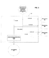
- FIG. 1 is a block diagram depicting a normal shared IO architecture having a standard PCIe switch 102 controlled by management host 104 running switch management software.
- Switch 102 services one or more hosts, shown as connected host 106 and connected host 108 (also referred to as "local hosts"), for example servers, PCs, and other computing devices.
- Also connected to switch are one or more devices 110-116 that typically provide some type of function or service for the connected hosts.
- virtual devices 118-124 Within switch 102 are virtual devices 118-124. Virtual devices 118 and 120 are connected to connected host 106 and virtual devices 122 and 124 are connected to connected host 108. Some of these virtual devices have data paths to physical devices 110-114. The functionality and roles of virtual devices 118-124 are described in U.S. Patent No.
- a method of enabling operation of a synthetic device in a PCIe switch according to claim 1.
- One aspect is a method of enhancing the functionality of a PCI express switch by enabling operation of a non-existent, logical (or synthetic) device in the switch.
- the logical device is implemented by logical device software in a management system host that controls operations of the switch.
- the synthetic device is presented to a local host connected to the switch. Write operations within the local host are captured thereby enabling the management system to create a shadow copy of local host component queues.
- the local host loads a driver for the synthetic device. Writes that occur in the local host are reflected in the management system. Shadow queues are created on the management system that reflects command and response queues in the local host.
- a DMA engine associated with the local host port is set up to automatically trigger on queues in the local host.
- the components, process steps, and/or data structures may be implemented using various types of operating systems, programming languages, computing platforms, computer programs, and/or general purpose machines.
- devices of a less general purpose nature such as hardwired devices, field programmable gate arrays (FPGAs), application specific integrated circuits (ASICs), or the like, may also be used.
- the present invention may also be tangibly embodied as a set of computer instructions stored on a computer readable medium, such as a memory device.
- any device driver model that uses a command queue and completion or response queue FIFO model with doorbells and interrupts for those FIFOs can be presented to connected hosts using the methods and systems described below. Before proceeding, it is useful to describe the basic components.
- One, as noted, is a FIFO model for input and output from a connected host driver to a DMA engine using the connected host memory.
- Interrupts are used for each completion or response queue for each completion queue for load balancing and indicating work completion.
- PCIe switches such as the Capella 2 switch from PLX Technologies of Sunnyvale, California.
- the figures below describe the additional features needed by the innovative PCIe switch of the present invention. Provided first is an overview of these additional features.
- the DMA engine (part of the switch port) transfers the queued work request in the command queue automatically to the management system, also referred to as a consumer/consolidation system.
- Another feature is a direct data path from the physical devices to the connected host. While commands (control path) go through the management system (MCPU), the data path is allowed to go directly from the physical device to the connected host. This provides a significant performance benefit and improves latency by preventing a bottleneck at the management system. For example, typical devices (including SSD storage) will do DMA requests from the device to the connected host memory (either read or writes) and these will go directly from the physical device to the connected host.
- Another feature is address isolation and the ability to access different connected hosts from any physical device endpoint. This may be enabled through address mapping/trapping features of the hardware enabled by the management system software. To present a logical device to a connected host requires that the switch trap connected host I/O enumeration cycles and also answer them correctly using the logical device software in the management system.
- a logical or non-existent device connected to a PCIe switch is presented or shown to a connected host (a host connected to the PCIe switch).
- the logical device does not physically exist (it is non-existent), thereby enabling connection of a fictitious device to a connected host at any time.
- the logical device is a synthetic I/O consolidation PCIe endpoint. This logical device provides a mechanism for consolidation of physical devices.
- the logical device may also be a pure software created device without it corresponding to any physical devices (i.e., there are no physical devices behind it).
- the logical device shows up as a PCIe endpoint or as a specific implementation or deployment, such as a RAID device. It uses specific software and hardware acceleration features of the PCIe switch.
- FIG. 2 is a block diagram depicting a PCIe switch having a logical device and a management host system with logical device enabling software in accordance with one embodiment. Shown is an innovative PCIe switch 202 connected to a host 204 and three physical devices 206-210. A management system host 212 with logical device software and other necessary software for operating the management system is connected to switch 202. The logical device enabling software implements a logical device 214 (also referred to as a consolidated virtual device) shown by the dashed-line box. Logical device 214 operates virtually with connected host 204. It has data paths going to physical devices 206-210. Management system host 212 has control paths shown by the dashed lines to the physical devices 206-210 that implement logical device 214. These control paths are dashed to indicate that they essentially emanate from the logical device enabling software in management system 212 and are responsible for physically implementing logical (virtual) device 214.
- logical device 214 also referred to as a consolidated virtual device
- one method of implementing the logical device to the PCIe switch utilizes DMA engines in a new capacity, address mapping and translation and configuration, and memory space and configuration space redirection features.
- the address mapping may be needed so that Base Address Registers (BARs) in the logical device are mapped to the management memory by software in the host management system.
- BARs Base Address Registers
- features of various physical devices are consolidated under one logical device.
- Another advantage is that if one physical device has an error or becomes disabled, then the logical device can still operate (e.g., the host system will not encounter a 'blue screen' scenario). Interrupt consolidation and generation is also possible, thereby easing the load on the host system.
- the logical device can be an NVMe endpoint which may consolidate physical NVMe or non-NVMe storage devices (e.g., SATA drives, SSC drives).
- the present invention addresses presenting a logical, non-existent device to a host by mapping address spaces for the logical device into a host management system CPU.
- the logical device is also tied to a DMA engine, thus, when the device is presented to a host, the host is able to see only the logical device and not the DMA functions.
- a connected host will not see or be aware of the underlying DMA or non-transparent (NT), even though the DMA and NT functions are operating, but just not shown to the host.
- the DMA engine is attached to queues and doorbells as explained below. Queues are allocated in host memory and written to the logical device. Queues are mapped into the host management system memory (FIFO). The DMA is then programmed to tie the queues in the logical device to host system memory queues. In addition, doorbells in the connected host may also be mapped to the host management system doorbell stack. As is known in the art, a device driver sends commands to a command queue in the device. There may be one or more command queues. The hardware performs operations on the data in the command queue and the results are stored in a response queue. As noted, the logical device has a FIFO for implementing these queues and a DMA engine is attached to them or is programmed to tie to the queues in the logical device.
- FIFO host management system memory
- the logical device DMA engine wakes up since it is tied to the logical device and more specifically is aware of the logical device command queue.
- the DMA engine transports this to management system interrupts. The work requested by the connected host is inserted in the queue and the process follows its normal course of operation.
- the logical software on the host is able to perform the work without extraneous or additional software on the host. It can be done solely with hardware assistance.
- the connected host driver writes operations to the device configuration space or BARs. Specifically, it will write to the device's registers in the BAR that are reflected in a shadow space in the host management system memory. As such, shadow copies of BARS are on the host management system. Thus, when there is a write to the BARs in the logical device, it is reflected in the management system.
- the shadow memory in the host management system captures writes that are originally in the connected host.
- the connected host loads a driver, it starts using registers in the BAR which is specific to device that is presented.
- the driver begins operating, configuring commands, and bringing up the device.
- the PCIe switch re-directs all writes and commands into the management system. As noted all writes in the connected host will appear in the host management system shadow memory via the PCIe switch.
- One step is setting up the data command and response queues on the local host memory.
- Commands for setting up or configuring the space (such as how many queues need to be supported, the number of logical disks, etc.) and other configuration questions may be answered or tended to by the logical software on the host management system.
- the driver configures the queues by allocating local system memory for the FIFO and writing base address and size to the hardware.
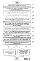
- FIG. 3 is a flow diagram of a process of installing a synthetic or logical device on a PCIe switch in accordance with one embodiment.
- the synthetic device is presented on or shown to a local host connected to the switch.
- the local host (herein "host") enumerates devices on the PCIe by performing configuration cycles on a bus captured by the device. This is described in the parent patent application.
- the host system software writes BARs on the configuration space and enables the logical device.
- the switch captures the writes at step 304 thereby enabling the management system to build the same configuration as on the local host. It can allocate the same memory space so there is a one-to-one mapping within the BARs and memory space. Thus, there is now a shadow copy of the local host BAR in the management system.
- the local host loads a driver for the logical device.
- the management system is notified of the same operations via the switch. That is, when the local host writes something to the BARs in the host memory, these writes will be reflected in the shadow memory in the management system.
- the local host driver performs driver initialization and device configuration queries. The management system is notified of these via the switch.
- all writes in the local host appear in the shadow memory on the management system. The driver performs set-up commands.
- the driver sets up queues for commands and responses in the local host as it normally would. These FIFO queues for storing commands and responses are known in the art.
- shadow queues are created by software on the management system and stored in memory. The queues in the local host are essentially mapped to the management system memory.
- the DMA engine for the port of the local host is set up to automatically trigger on queues on the local host. That is, the DMA engine is programmed to tie the command queue in the local host to the command queue in the management system memory. This mapping is also done with the doorbells in the local host at step 218. Therefore, when the host driver rings the doorbell, the DMA wakes up (i.e., is automatically triggered).
- the local host driver sets up interrupt vectors and handlers on the local host. These interrupts are sent to the management system at which time one of two different actions may occur.
- the management system stores the interrupt vectors for direct access during runtime.
- the interrupt vector is associated with the DMA engine queues that will manage the local host response queues. At this stage the installation of the logical device on the PCIe switch is complete.
- the logical device is implemented by software in the management system. It is this software that does work on the data and directs it to the physical device.
- a completion signal is sent to the management system which ordered the work via logical device software where the features of the physical device are consolidated.
- the response from the work is sent directly to the local host where it is stored in the response queue. This update to the local host response queue is still reflected in shadow memory of the management system.
- the description herein provides a number of new features and improvements to existing PCIe switching technology.
- hardware assists to enable I/O physical device consolidation is described, while adding or enabling value-added features using this consolidation. Separation and isolation of hot-plug events from the connected physical devices to the connected port through the use of a logical or synthetic endpoint in the connected host is described. There are also performance improvements by virtue of the consolidation and isolation of interrupts generated by connected physical devices to a connected host.
- the embodiments described above are extensible with software in the management system. There can be multiple hosts and physical devices (e.g., there can be 15 physical devices being shadowed by 5 connected hosts all connected to one PCIe switch).
- the various aspects, embodiments, implementations or features of the described embodiments can be used separately or in any combination.
- Various aspects of the described embodiments can be implemented by software, hardware or a combination of hardware and software.
- the described embodiments can also be embodied as computer readable code on a computer readable medium.
- the computer readable medium is defined as any data storage device that can store data which can thereafter be read by a computer system. Examples of the computer readable medium include read-only memory, random-access memory, CD-ROMs, DVDs, magnetic tape, and optical data storage devices.
- the computer readable medium can also be distributed over network-coupled computer systems so that the computer readable code is stored and executed in a distributed fashion.
Landscapes
- Engineering & Computer Science (AREA)
- Physics & Mathematics (AREA)
- General Engineering & Computer Science (AREA)
- Theoretical Computer Science (AREA)
- Mathematical Physics (AREA)
- Computer Hardware Design (AREA)
- General Physics & Mathematics (AREA)
- Bus Control (AREA)
- Information Transfer Systems (AREA)
Applications Claiming Priority (1)
| Application Number | Priority Date | Filing Date | Title |
|---|---|---|---|
| US13/624,781 US9141571B2 (en) | 2010-12-28 | 2012-09-21 | PCI express switch with logical device capability |
Publications (3)
| Publication Number | Publication Date |
|---|---|
| EP2711845A2 EP2711845A2 (en) | 2014-03-26 |
| EP2711845A3 EP2711845A3 (en) | 2014-10-01 |
| EP2711845B1 true EP2711845B1 (en) | 2015-12-02 |
Family
ID=49263122
Family Applications (1)
| Application Number | Title | Priority Date | Filing Date |
|---|---|---|---|
| EP13185535.5A Active EP2711845B1 (en) | 2012-09-21 | 2013-09-23 | PCI express switch with logical device capability |
Country Status (4)
| Country | Link |
|---|---|
| EP (1) | EP2711845B1 (enExample) |
| JP (1) | JP2014063497A (enExample) |
| CN (1) | CN103678201B (enExample) |
| TW (1) | TW201415236A (enExample) |
Cited By (1)
| Publication number | Priority date | Publication date | Assignee | Title |
|---|---|---|---|---|
| US10901638B2 (en) | 2016-03-01 | 2021-01-26 | Huawei Technologies Co., Ltd. | Cascading board and SSD shared remote access system and method |
Families Citing this family (13)
| Publication number | Priority date | Publication date | Assignee | Title |
|---|---|---|---|---|
| CN104536701B (zh) * | 2014-12-23 | 2018-02-06 | 记忆科技(深圳)有限公司 | 一种nvme协议多命令队列的实现方法及系统 |
| US10140057B2 (en) * | 2016-02-18 | 2018-11-27 | Micron Technology, Inc. | Apparatuses and methods for multiple address registers for a solid state device |
| US10515032B2 (en) * | 2016-07-01 | 2019-12-24 | Intel Corporation | Asymmetric transmission (TX) and receive (RX) lanes in a point-to-point interconnect using a peripheral component interconnect express (PCIE) resources in a computer system |
| US10992967B2 (en) * | 2017-12-05 | 2021-04-27 | Sony Interactive Entertainment LLC | Ultra high-speed low-latency network storage |
| US12481612B2 (en) | 2018-03-02 | 2025-11-25 | Samsung Electronics Co., Ltd. | Mechanism to identify FPGA and SSD pairing in a multi-device environment |
| US10635609B2 (en) | 2018-03-02 | 2020-04-28 | Samsung Electronics Co., Ltd. | Method for supporting erasure code data protection with embedded PCIE switch inside FPGA+SSD |
| CN110865960B (zh) * | 2018-08-28 | 2022-07-22 | 上海忆芯实业有限公司 | 在网络上模拟PCIe总线 |
| TWI791880B (zh) * | 2018-10-12 | 2023-02-11 | 南韓商三星電子股份有限公司 | 電腦系統 |
| CN110659122A (zh) * | 2019-07-31 | 2020-01-07 | 杭州阿姆科技有限公司 | 一种ssd中断实现方法及装置 |
| CN112732166B (zh) * | 2019-10-28 | 2024-06-18 | 华为技术有限公司 | 访问固态硬盘的方法及装置 |
| CN112256601B (zh) * | 2020-10-19 | 2023-04-21 | 苏州凌云光工业智能技术有限公司 | 数据存取控制方法、嵌入式存储系统及嵌入式设备 |
| CN114138702B (zh) * | 2022-01-29 | 2022-06-14 | 阿里云计算有限公司 | 计算系统、pci设备管理器及其初始化方法 |
| CN119814820A (zh) * | 2024-12-19 | 2025-04-11 | 国网上海市电力公司 | 一种变配电站数据汇集系统及方法 |
Family Cites Families (7)
| Publication number | Priority date | Publication date | Assignee | Title |
|---|---|---|---|---|
| US7293129B2 (en) * | 2005-04-22 | 2007-11-06 | Sun Microsystems, Inc. | Flexible routing and addressing |
| US20080313364A1 (en) * | 2006-12-06 | 2008-12-18 | David Flynn | Apparatus, system, and method for remote direct memory access to a solid-state storage device |
| CN101277195B (zh) * | 2007-03-30 | 2011-12-07 | 杭州华三通信技术有限公司 | 一种交换网通信系统、实现方法及交换装置 |
| CN101159649B (zh) * | 2007-09-21 | 2010-04-14 | 杭州华三通信技术有限公司 | 一种pci快速总线系统及其能量管理方法 |
| CN100478935C (zh) * | 2007-10-10 | 2009-04-15 | 福建星网锐捷网络有限公司 | Pcie通道扩展装置、系统及其配置方法 |
| US7934033B2 (en) * | 2008-03-25 | 2011-04-26 | Aprius, Inc. | PCI-express function proxy |
| US8521941B2 (en) | 2010-12-28 | 2013-08-27 | Plx Technology, Inc. | Multi-root sharing of single-root input/output virtualization |
-
2013
- 2013-09-20 JP JP2013195758A patent/JP2014063497A/ja not_active Withdrawn
- 2013-09-23 EP EP13185535.5A patent/EP2711845B1/en active Active
- 2013-09-23 TW TW102134179A patent/TW201415236A/zh unknown
- 2013-09-23 CN CN201310536515.9A patent/CN103678201B/zh active Active
Cited By (1)
| Publication number | Priority date | Publication date | Assignee | Title |
|---|---|---|---|---|
| US10901638B2 (en) | 2016-03-01 | 2021-01-26 | Huawei Technologies Co., Ltd. | Cascading board and SSD shared remote access system and method |
Also Published As
| Publication number | Publication date |
|---|---|
| CN103678201B (zh) | 2017-12-22 |
| CN103678201A (zh) | 2014-03-26 |
| EP2711845A3 (en) | 2014-10-01 |
| TW201415236A (zh) | 2014-04-16 |
| JP2014063497A (ja) | 2014-04-10 |
| EP2711845A2 (en) | 2014-03-26 |
Similar Documents
| Publication | Publication Date | Title |
|---|---|---|
| US9141571B2 (en) | PCI express switch with logical device capability | |
| EP2711845B1 (en) | PCI express switch with logical device capability | |
| CN104142849B (zh) | 多主机单根输入/输出虚拟化虚拟功能共享的方法及系统 | |
| US9223734B2 (en) | Switch with synthetic device capability | |
| US9262189B2 (en) | Configuring VM and IO storage adapter VF for virtual target addressing during direct data access | |
| US8645605B2 (en) | Sharing multiple virtual functions to a host using a pseudo physical function | |
| US8392623B2 (en) | Guest/hypervisor interrupt coalescing for storage adapter virtual function in guest passthrough mode | |
| US9037768B2 (en) | Virtual-interrupt-mode interface and method for virtualizing an interrupt mode | |
| US10846254B2 (en) | Management controller including virtual USB host controller | |
| US10261698B2 (en) | Systems and methods for hardware-based raid acceleration for variable-length and out-of-order transactions | |
| KR102568906B1 (ko) | PCIe 디바이스 및 그 동작 방법 | |
| CN108885572B (zh) | 安全驱动程序平台 | |
| US7958293B2 (en) | Virtualized serial attached SCSI adapter | |
| CN114417373B (zh) | 一种NVMe-oF用户态客户端的数据访问方法和装置 | |
| CN101470596B (zh) | 虚拟化环境中的音频子系统共享 | |
| WO2010077813A2 (en) | Composite device emulation | |
| US10261699B2 (en) | Systems and methods for hardware-based RAID acceleration | |
| US20250077454A1 (en) | Peripheral component interconnect express device and operating method thereof | |
| JP6760579B2 (ja) | ネットワークラインカード(lc)のホストオペレーティングシステム(os)への統合 | |
| US7930445B2 (en) | Computer system using remote I/O and I/O data transfer method | |
| US20150254082A1 (en) | Remote booting over pci express using synthetic remote boot capability | |
| US20240095205A1 (en) | User-defined peripheral-bus device implementation | |
| JP6245370B2 (ja) | コンピュータシステム及びデータを双方向に送受信する方法 | |
| US8095715B1 (en) | SCSI HBA management using logical units | |
| WO2009113571A1 (ja) | 複数の基盤ソフトウェアを動作可能な情報処理装置および方法 |
Legal Events
| Date | Code | Title | Description |
|---|---|---|---|
| PUAI | Public reference made under article 153(3) epc to a published international application that has entered the european phase |
Free format text: ORIGINAL CODE: 0009012 |
|
| 17P | Request for examination filed |
Effective date: 20131003 |
|
| AK | Designated contracting states |
Kind code of ref document: A2 Designated state(s): AL AT BE BG CH CY CZ DE DK EE ES FI FR GB GR HR HU IE IS IT LI LT LU LV MC MK MT NL NO PL PT RO RS SE SI SK SM TR |
|
| AX | Request for extension of the european patent |
Extension state: BA ME |
|
| PUAL | Search report despatched |
Free format text: ORIGINAL CODE: 0009013 |
|
| AK | Designated contracting states |
Kind code of ref document: A3 Designated state(s): AL AT BE BG CH CY CZ DE DK EE ES FI FR GB GR HR HU IE IS IT LI LT LU LV MC MK MT NL NO PL PT RO RS SE SI SK SM TR |
|
| AX | Request for extension of the european patent |
Extension state: BA ME |
|
| RIC1 | Information provided on ipc code assigned before grant |
Ipc: G06F 13/40 20060101AFI20140828BHEP |
|
| GRAP | Despatch of communication of intention to grant a patent |
Free format text: ORIGINAL CODE: EPIDOSNIGR1 |
|
| INTG | Intention to grant announced |
Effective date: 20150610 |
|
| GRAS | Grant fee paid |
Free format text: ORIGINAL CODE: EPIDOSNIGR3 |
|
| GRAA | (expected) grant |
Free format text: ORIGINAL CODE: 0009210 |
|
| RAP1 | Party data changed (applicant data changed or rights of an application transferred) |
Owner name: AVAGO TECHNOLOGIES GENERAL IP (SINGAPORE) PTE. LTD |
|
| AK | Designated contracting states |
Kind code of ref document: B1 Designated state(s): AL AT BE BG CH CY CZ DE DK EE ES FI FR GB GR HR HU IE IS IT LI LT LU LV MC MK MT NL NO PL PT RO RS SE SI SK SM TR |
|
| REG | Reference to a national code |
Ref country code: GB Ref legal event code: FG4D |
|
| REG | Reference to a national code |
Ref country code: AT Ref legal event code: REF Ref document number: 763904 Country of ref document: AT Kind code of ref document: T Effective date: 20151215 Ref country code: CH Ref legal event code: EP |
|
| REG | Reference to a national code |
Ref country code: IE Ref legal event code: FG4D |
|
| REG | Reference to a national code |
Ref country code: DE Ref legal event code: R096 Ref document number: 602013003987 Country of ref document: DE |
|
| REG | Reference to a national code |
Ref country code: NL Ref legal event code: MP Effective date: 20160302 |
|
| REG | Reference to a national code |
Ref country code: LT Ref legal event code: MG4D |
|
| REG | Reference to a national code |
Ref country code: AT Ref legal event code: MK05 Ref document number: 763904 Country of ref document: AT Kind code of ref document: T Effective date: 20151202 |
|
| PG25 | Lapsed in a contracting state [announced via postgrant information from national office to epo] |
Ref country code: LT Free format text: LAPSE BECAUSE OF FAILURE TO SUBMIT A TRANSLATION OF THE DESCRIPTION OR TO PAY THE FEE WITHIN THE PRESCRIBED TIME-LIMIT Effective date: 20151202 Ref country code: ES Free format text: LAPSE BECAUSE OF FAILURE TO SUBMIT A TRANSLATION OF THE DESCRIPTION OR TO PAY THE FEE WITHIN THE PRESCRIBED TIME-LIMIT Effective date: 20151202 Ref country code: NO Free format text: LAPSE BECAUSE OF FAILURE TO SUBMIT A TRANSLATION OF THE DESCRIPTION OR TO PAY THE FEE WITHIN THE PRESCRIBED TIME-LIMIT Effective date: 20160302 |
|
| PG25 | Lapsed in a contracting state [announced via postgrant information from national office to epo] |
Ref country code: PL Free format text: LAPSE BECAUSE OF FAILURE TO SUBMIT A TRANSLATION OF THE DESCRIPTION OR TO PAY THE FEE WITHIN THE PRESCRIBED TIME-LIMIT Effective date: 20151202 Ref country code: SE Free format text: LAPSE BECAUSE OF FAILURE TO SUBMIT A TRANSLATION OF THE DESCRIPTION OR TO PAY THE FEE WITHIN THE PRESCRIBED TIME-LIMIT Effective date: 20151202 Ref country code: AT Free format text: LAPSE BECAUSE OF FAILURE TO SUBMIT A TRANSLATION OF THE DESCRIPTION OR TO PAY THE FEE WITHIN THE PRESCRIBED TIME-LIMIT Effective date: 20151202 Ref country code: RS Free format text: LAPSE BECAUSE OF FAILURE TO SUBMIT A TRANSLATION OF THE DESCRIPTION OR TO PAY THE FEE WITHIN THE PRESCRIBED TIME-LIMIT Effective date: 20151202 Ref country code: GR Free format text: LAPSE BECAUSE OF FAILURE TO SUBMIT A TRANSLATION OF THE DESCRIPTION OR TO PAY THE FEE WITHIN THE PRESCRIBED TIME-LIMIT Effective date: 20160303 Ref country code: FI Free format text: LAPSE BECAUSE OF FAILURE TO SUBMIT A TRANSLATION OF THE DESCRIPTION OR TO PAY THE FEE WITHIN THE PRESCRIBED TIME-LIMIT Effective date: 20151202 Ref country code: LV Free format text: LAPSE BECAUSE OF FAILURE TO SUBMIT A TRANSLATION OF THE DESCRIPTION OR TO PAY THE FEE WITHIN THE PRESCRIBED TIME-LIMIT Effective date: 20151202 Ref country code: NL Free format text: LAPSE BECAUSE OF FAILURE TO SUBMIT A TRANSLATION OF THE DESCRIPTION OR TO PAY THE FEE WITHIN THE PRESCRIBED TIME-LIMIT Effective date: 20151202 |
|
| PG25 | Lapsed in a contracting state [announced via postgrant information from national office to epo] |
Ref country code: IS Free format text: LAPSE BECAUSE OF FAILURE TO SUBMIT A TRANSLATION OF THE DESCRIPTION OR TO PAY THE FEE WITHIN THE PRESCRIBED TIME-LIMIT Effective date: 20151202 |
|
| PG25 | Lapsed in a contracting state [announced via postgrant information from national office to epo] |
Ref country code: IT Free format text: LAPSE BECAUSE OF FAILURE TO SUBMIT A TRANSLATION OF THE DESCRIPTION OR TO PAY THE FEE WITHIN THE PRESCRIBED TIME-LIMIT Effective date: 20151202 Ref country code: CZ Free format text: LAPSE BECAUSE OF FAILURE TO SUBMIT A TRANSLATION OF THE DESCRIPTION OR TO PAY THE FEE WITHIN THE PRESCRIBED TIME-LIMIT Effective date: 20151202 |
|
| PG25 | Lapsed in a contracting state [announced via postgrant information from national office to epo] |
Ref country code: IS Free format text: LAPSE BECAUSE OF FAILURE TO SUBMIT A TRANSLATION OF THE DESCRIPTION OR TO PAY THE FEE WITHIN THE PRESCRIBED TIME-LIMIT Effective date: 20160402 Ref country code: PT Free format text: LAPSE BECAUSE OF FAILURE TO SUBMIT A TRANSLATION OF THE DESCRIPTION OR TO PAY THE FEE WITHIN THE PRESCRIBED TIME-LIMIT Effective date: 20160404 Ref country code: SK Free format text: LAPSE BECAUSE OF FAILURE TO SUBMIT A TRANSLATION OF THE DESCRIPTION OR TO PAY THE FEE WITHIN THE PRESCRIBED TIME-LIMIT Effective date: 20151202 Ref country code: SM Free format text: LAPSE BECAUSE OF FAILURE TO SUBMIT A TRANSLATION OF THE DESCRIPTION OR TO PAY THE FEE WITHIN THE PRESCRIBED TIME-LIMIT Effective date: 20151202 Ref country code: EE Free format text: LAPSE BECAUSE OF FAILURE TO SUBMIT A TRANSLATION OF THE DESCRIPTION OR TO PAY THE FEE WITHIN THE PRESCRIBED TIME-LIMIT Effective date: 20151202 Ref country code: RO Free format text: LAPSE BECAUSE OF FAILURE TO SUBMIT A TRANSLATION OF THE DESCRIPTION OR TO PAY THE FEE WITHIN THE PRESCRIBED TIME-LIMIT Effective date: 20151202 |
|
| REG | Reference to a national code |
Ref country code: DE Ref legal event code: R097 Ref document number: 602013003987 Country of ref document: DE |
|
| PLBE | No opposition filed within time limit |
Free format text: ORIGINAL CODE: 0009261 |
|
| STAA | Information on the status of an ep patent application or granted ep patent |
Free format text: STATUS: NO OPPOSITION FILED WITHIN TIME LIMIT |
|
| PG25 | Lapsed in a contracting state [announced via postgrant information from national office to epo] |
Ref country code: DK Free format text: LAPSE BECAUSE OF FAILURE TO SUBMIT A TRANSLATION OF THE DESCRIPTION OR TO PAY THE FEE WITHIN THE PRESCRIBED TIME-LIMIT Effective date: 20151202 |
|
| 26N | No opposition filed |
Effective date: 20160905 |
|
| PG25 | Lapsed in a contracting state [announced via postgrant information from national office to epo] |
Ref country code: SI Free format text: LAPSE BECAUSE OF FAILURE TO SUBMIT A TRANSLATION OF THE DESCRIPTION OR TO PAY THE FEE WITHIN THE PRESCRIBED TIME-LIMIT Effective date: 20151202 |
|
| PG25 | Lapsed in a contracting state [announced via postgrant information from national office to epo] |
Ref country code: BE Free format text: LAPSE BECAUSE OF FAILURE TO SUBMIT A TRANSLATION OF THE DESCRIPTION OR TO PAY THE FEE WITHIN THE PRESCRIBED TIME-LIMIT Effective date: 20151202 |
|
| PG25 | Lapsed in a contracting state [announced via postgrant information from national office to epo] |
Ref country code: MC Free format text: LAPSE BECAUSE OF FAILURE TO SUBMIT A TRANSLATION OF THE DESCRIPTION OR TO PAY THE FEE WITHIN THE PRESCRIBED TIME-LIMIT Effective date: 20151202 |
|
| REG | Reference to a national code |
Ref country code: CH Ref legal event code: PL |
|
| REG | Reference to a national code |
Ref country code: IE Ref legal event code: MM4A |
|
| REG | Reference to a national code |
Ref country code: FR Ref legal event code: ST Effective date: 20170531 |
|
| PG25 | Lapsed in a contracting state [announced via postgrant information from national office to epo] |
Ref country code: LI Free format text: LAPSE BECAUSE OF NON-PAYMENT OF DUE FEES Effective date: 20160930 Ref country code: FR Free format text: LAPSE BECAUSE OF NON-PAYMENT OF DUE FEES Effective date: 20160930 Ref country code: CH Free format text: LAPSE BECAUSE OF NON-PAYMENT OF DUE FEES Effective date: 20160930 Ref country code: IE Free format text: LAPSE BECAUSE OF NON-PAYMENT OF DUE FEES Effective date: 20160923 |
|
| PG25 | Lapsed in a contracting state [announced via postgrant information from national office to epo] |
Ref country code: LU Free format text: LAPSE BECAUSE OF NON-PAYMENT OF DUE FEES Effective date: 20160923 |
|
| GBPC | Gb: european patent ceased through non-payment of renewal fee |
Effective date: 20170923 |
|
| PG25 | Lapsed in a contracting state [announced via postgrant information from national office to epo] |
Ref country code: CY Free format text: LAPSE BECAUSE OF FAILURE TO SUBMIT A TRANSLATION OF THE DESCRIPTION OR TO PAY THE FEE WITHIN THE PRESCRIBED TIME-LIMIT Effective date: 20151202 Ref country code: HU Free format text: LAPSE BECAUSE OF FAILURE TO SUBMIT A TRANSLATION OF THE DESCRIPTION OR TO PAY THE FEE WITHIN THE PRESCRIBED TIME-LIMIT; INVALID AB INITIO Effective date: 20130923 |
|
| PG25 | Lapsed in a contracting state [announced via postgrant information from national office to epo] |
Ref country code: MT Free format text: LAPSE BECAUSE OF NON-PAYMENT OF DUE FEES Effective date: 20160930 Ref country code: HR Free format text: LAPSE BECAUSE OF FAILURE TO SUBMIT A TRANSLATION OF THE DESCRIPTION OR TO PAY THE FEE WITHIN THE PRESCRIBED TIME-LIMIT Effective date: 20151202 Ref country code: MK Free format text: LAPSE BECAUSE OF FAILURE TO SUBMIT A TRANSLATION OF THE DESCRIPTION OR TO PAY THE FEE WITHIN THE PRESCRIBED TIME-LIMIT Effective date: 20151202 |
|
| PG25 | Lapsed in a contracting state [announced via postgrant information from national office to epo] |
Ref country code: BG Free format text: LAPSE BECAUSE OF FAILURE TO SUBMIT A TRANSLATION OF THE DESCRIPTION OR TO PAY THE FEE WITHIN THE PRESCRIBED TIME-LIMIT Effective date: 20151202 Ref country code: GB Free format text: LAPSE BECAUSE OF NON-PAYMENT OF DUE FEES Effective date: 20170923 |
|
| PG25 | Lapsed in a contracting state [announced via postgrant information from national office to epo] |
Ref country code: TR Free format text: LAPSE BECAUSE OF FAILURE TO SUBMIT A TRANSLATION OF THE DESCRIPTION OR TO PAY THE FEE WITHIN THE PRESCRIBED TIME-LIMIT Effective date: 20151202 Ref country code: AL Free format text: LAPSE BECAUSE OF FAILURE TO SUBMIT A TRANSLATION OF THE DESCRIPTION OR TO PAY THE FEE WITHIN THE PRESCRIBED TIME-LIMIT Effective date: 20151202 |
|
| REG | Reference to a national code |
Ref country code: DE Ref legal event code: R081 Ref document number: 602013003987 Country of ref document: DE Owner name: AVAGO TECHNOLOGIES INTERNATIONAL SALES PTE. LT, SG Free format text: FORMER OWNER: AVAGO TECHNOLOGIES GENERAL IP (SINGAPORE) PTE. LTD., SINGAPORE, SG Ref country code: DE Ref legal event code: R082 Ref document number: 602013003987 Country of ref document: DE Representative=s name: DILG, HAEUSLER, SCHINDELMANN PATENTANWALTSGESE, DE Ref country code: DE Ref legal event code: R082 Ref document number: 602013003987 Country of ref document: DE Representative=s name: DILG HAEUSLER SCHINDELMANN PATENTANWALTSGESELL, DE |
|
| PGFP | Annual fee paid to national office [announced via postgrant information from national office to epo] |
Ref country code: DE Payment date: 20250910 Year of fee payment: 13 |