EP2711161A1 - Nanoimprint mold and curved body - Google Patents
Nanoimprint mold and curved body Download PDFInfo
- Publication number
- EP2711161A1 EP2711161A1 EP20120785578 EP12785578A EP2711161A1 EP 2711161 A1 EP2711161 A1 EP 2711161A1 EP 20120785578 EP20120785578 EP 20120785578 EP 12785578 A EP12785578 A EP 12785578A EP 2711161 A1 EP2711161 A1 EP 2711161A1
- Authority
- EP
- European Patent Office
- Prior art keywords
- mold
- curved surface
- silicone rubber
- resin
- nanoimprint mold
- Prior art date
- Legal status (The legal status is an assumption and is not a legal conclusion. Google has not performed a legal analysis and makes no representation as to the accuracy of the status listed.)
- Withdrawn
Links
- 229920002379 silicone rubber Polymers 0.000 claims abstract description 44
- 239000004945 silicone rubber Substances 0.000 claims abstract description 42
- 229920001971 elastomer Polymers 0.000 claims abstract description 17
- 239000005060 rubber Substances 0.000 claims abstract description 17
- 239000000758 substrate Substances 0.000 claims description 19
- 238000002834 transmittance Methods 0.000 claims description 6
- 229920001187 thermosetting polymer Polymers 0.000 claims description 3
- 229920005989 resin Polymers 0.000 description 26
- 239000011347 resin Substances 0.000 description 26
- 238000012546 transfer Methods 0.000 description 16
- 229920001296 polysiloxane Polymers 0.000 description 14
- 229920005992 thermoplastic resin Polymers 0.000 description 8
- 239000011521 glass Substances 0.000 description 5
- 239000005020 polyethylene terephthalate Substances 0.000 description 4
- 229920000139 polyethylene terephthalate Polymers 0.000 description 4
- 239000000463 material Substances 0.000 description 3
- 239000000203 mixture Substances 0.000 description 3
- 230000000877 morphologic effect Effects 0.000 description 3
- 238000002360 preparation method Methods 0.000 description 3
- 230000000052 comparative effect Effects 0.000 description 2
- 238000005259 measurement Methods 0.000 description 2
- 239000002184 metal Substances 0.000 description 2
- 125000005375 organosiloxane group Chemical group 0.000 description 2
- 229920003229 poly(methyl methacrylate) Polymers 0.000 description 2
- -1 polyethylene terephthalate Polymers 0.000 description 2
- 239000004926 polymethyl methacrylate Substances 0.000 description 2
- 238000001029 thermal curing Methods 0.000 description 2
- ILBBNQMSDGAAPF-UHFFFAOYSA-N 1-(6-hydroxy-6-methylcyclohexa-2,4-dien-1-yl)propan-1-one Chemical compound CCC(=O)C1C=CC=CC1(C)O ILBBNQMSDGAAPF-UHFFFAOYSA-N 0.000 description 1
- 239000004925 Acrylic resin Substances 0.000 description 1
- 229920000178 Acrylic resin Polymers 0.000 description 1
- 230000001588 bifunctional effect Effects 0.000 description 1
- 239000003054 catalyst Substances 0.000 description 1
- 238000004891 communication Methods 0.000 description 1
- 238000001816 cooling Methods 0.000 description 1
- 238000001723 curing Methods 0.000 description 1
- 230000000694 effects Effects 0.000 description 1
- 230000001678 irradiating effect Effects 0.000 description 1
- 239000007788 liquid Substances 0.000 description 1
- 238000000034 method Methods 0.000 description 1
- 230000003287 optical effect Effects 0.000 description 1
- 230000002093 peripheral effect Effects 0.000 description 1
- 239000004417 polycarbonate Substances 0.000 description 1
- 229920000515 polycarbonate Polymers 0.000 description 1
- 229920000642 polymer Polymers 0.000 description 1
- 238000003825 pressing Methods 0.000 description 1
- 239000010453 quartz Substances 0.000 description 1
- 238000011160 research Methods 0.000 description 1
- VYPSYNLAJGMNEJ-UHFFFAOYSA-N silicon dioxide Inorganic materials O=[Si]=O VYPSYNLAJGMNEJ-UHFFFAOYSA-N 0.000 description 1
- 238000004528 spin coating Methods 0.000 description 1
- 238000009281 ultraviolet germicidal irradiation Methods 0.000 description 1
Images


Classifications
-
- B—PERFORMING OPERATIONS; TRANSPORTING
- B29—WORKING OF PLASTICS; WORKING OF SUBSTANCES IN A PLASTIC STATE IN GENERAL
- B29C—SHAPING OR JOINING OF PLASTICS; SHAPING OF MATERIAL IN A PLASTIC STATE, NOT OTHERWISE PROVIDED FOR; AFTER-TREATMENT OF THE SHAPED PRODUCTS, e.g. REPAIRING
- B29C33/00—Moulds or cores; Details thereof or accessories therefor
- B29C33/42—Moulds or cores; Details thereof or accessories therefor characterised by the shape of the moulding surface, e.g. ribs or grooves
- B29C33/424—Moulding surfaces provided with means for marking or patterning
-
- B—PERFORMING OPERATIONS; TRANSPORTING
- B29—WORKING OF PLASTICS; WORKING OF SUBSTANCES IN A PLASTIC STATE IN GENERAL
- B29C—SHAPING OR JOINING OF PLASTICS; SHAPING OF MATERIAL IN A PLASTIC STATE, NOT OTHERWISE PROVIDED FOR; AFTER-TREATMENT OF THE SHAPED PRODUCTS, e.g. REPAIRING
- B29C59/00—Surface shaping of articles, e.g. embossing; Apparatus therefor
- B29C59/02—Surface shaping of articles, e.g. embossing; Apparatus therefor by mechanical means, e.g. pressing
-
- B—PERFORMING OPERATIONS; TRANSPORTING
- B29—WORKING OF PLASTICS; WORKING OF SUBSTANCES IN A PLASTIC STATE IN GENERAL
- B29C—SHAPING OR JOINING OF PLASTICS; SHAPING OF MATERIAL IN A PLASTIC STATE, NOT OTHERWISE PROVIDED FOR; AFTER-TREATMENT OF THE SHAPED PRODUCTS, e.g. REPAIRING
- B29C33/00—Moulds or cores; Details thereof or accessories therefor
- B29C33/38—Moulds or cores; Details thereof or accessories therefor characterised by the material or the manufacturing process
-
- B—PERFORMING OPERATIONS; TRANSPORTING
- B29—WORKING OF PLASTICS; WORKING OF SUBSTANCES IN A PLASTIC STATE IN GENERAL
- B29C—SHAPING OR JOINING OF PLASTICS; SHAPING OF MATERIAL IN A PLASTIC STATE, NOT OTHERWISE PROVIDED FOR; AFTER-TREATMENT OF THE SHAPED PRODUCTS, e.g. REPAIRING
- B29C33/00—Moulds or cores; Details thereof or accessories therefor
- B29C33/38—Moulds or cores; Details thereof or accessories therefor characterised by the material or the manufacturing process
- B29C33/40—Plastics, e.g. foam or rubber
- B29C33/405—Elastomers, e.g. rubber
-
- G—PHYSICS
- G03—PHOTOGRAPHY; CINEMATOGRAPHY; ANALOGOUS TECHNIQUES USING WAVES OTHER THAN OPTICAL WAVES; ELECTROGRAPHY; HOLOGRAPHY
- G03F—PHOTOMECHANICAL PRODUCTION OF TEXTURED OR PATTERNED SURFACES, e.g. FOR PRINTING, FOR PROCESSING OF SEMICONDUCTOR DEVICES; MATERIALS THEREFOR; ORIGINALS THEREFOR; APPARATUS SPECIALLY ADAPTED THEREFOR
- G03F7/00—Photomechanical, e.g. photolithographic, production of textured or patterned surfaces, e.g. printing surfaces; Materials therefor, e.g. comprising photoresists; Apparatus specially adapted therefor
- G03F7/0002—Lithographic processes using patterning methods other than those involving the exposure to radiation, e.g. by stamping
-
- B—PERFORMING OPERATIONS; TRANSPORTING
- B29—WORKING OF PLASTICS; WORKING OF SUBSTANCES IN A PLASTIC STATE IN GENERAL
- B29K—INDEXING SCHEME ASSOCIATED WITH SUBCLASSES B29B, B29C OR B29D, RELATING TO MOULDING MATERIALS OR TO MATERIALS FOR MOULDS, REINFORCEMENTS, FILLERS OR PREFORMED PARTS, e.g. INSERTS
- B29K2883/00—Use of polymers having silicon, with or without sulfur, nitrogen, oxygen, or carbon only, in the main chain, as mould material
-
- Y—GENERAL TAGGING OF NEW TECHNOLOGICAL DEVELOPMENTS; GENERAL TAGGING OF CROSS-SECTIONAL TECHNOLOGIES SPANNING OVER SEVERAL SECTIONS OF THE IPC; TECHNICAL SUBJECTS COVERED BY FORMER USPC CROSS-REFERENCE ART COLLECTIONS [XRACs] AND DIGESTS
- Y10—TECHNICAL SUBJECTS COVERED BY FORMER USPC
- Y10T—TECHNICAL SUBJECTS COVERED BY FORMER US CLASSIFICATION
- Y10T428/00—Stock material or miscellaneous articles
- Y10T428/24—Structurally defined web or sheet [e.g., overall dimension, etc.]
- Y10T428/24479—Structurally defined web or sheet [e.g., overall dimension, etc.] including variation in thickness
Definitions
- the present invention relates to a mold for forming depressions and protrusions of nanometer order and a curved surface body obtained by using the mold.
- a demultiplexing spectroscopic device For optical communication, a demultiplexing spectroscopic device has been used.
- a wavelength spectroscopic device to disperse a necessary wavelength is used.
- the demultiplexing spectroscopic device is formed on a flat surface of a transparent substrate, but the demultiplexing spectroscopic device must be sometimes formed on a curved surface such as a lens surface depending upon the use purpose.
- a rigid mother mold is formed, then a surface profile of this mother mold is transferred to a resin, and using the resulting resin mold, the demultiplexing spectroscopic device is formed.
- the resin is not specifically restricted provided that it is transparent and has certain strength, and a usual resin has been used.
- a mold consisting of a PET (polyethylene terephthalate) base and an acrylic resin laminated on the base is generally known (patent literature 1).
- a rigid layer formed from a material of high hardness is essential. Therefore, this mold hardly has stretchability, and imprinting can be made only on a substantially flat surface shape. On this account, it is necessary to prepare a mold that meets a mode in which a depression-protrusion profile of nanometer level is formed on a curved surface such as a lens surface.
- thermoplastic resin having a depression-protrusion profile on its surface has been allowed to adhere to a surface of a lens or the like, and the thermoplastic resin is relatively rigid. Therefore, there is a problem that this curved surface body cannot be applied to a member (lens or the like) having a large curvature radius.
- the nanoimprint mold of the present invention is characterized by comprising a silicone rubber elastic body having an Hs rubber hardness of 10 to 55 and by having fine depressions and protrusions formed on the surface.
- the silicone rubber elastic body for use in the present invention is ultraviolet curable silicone rubber or thermosetting silicone rubber.
- the total light transmittance of the silicone rubber (measured using a sheet having a thickness of 250 ⁇ m in accordance with JIS K7105) is not less than 60%, preferably not less than 80%, and a higher transparency is preferable.
- the silicone rubber elastic body having an Hs rubber hardness of 10 to 55 can be used alone, but the silicone rubber elastic body can be formed on a surface of a transparent substrate.
- the transparent substrate is preferably a curved surface body having a curved surface part having a curvature radius of not more than 500 mm.
- the curved surface body of the present invention is preferably a curved surface body having a curved surface part having a curvature radius of not more than 500 mm, and having depressions and protrusions having an interval of 50 to 100000 nm on the surface of the curved surface part.
- the nanoimprint mold of the present invention fine depressions and protrusions having been formed on a mother mold can be transferred from the mother mold to a surface of a silicone rubber elastic body having a specific hardness. Since this mother mold is formed from a rigid member such as silicone, glass or a metal and is extremely expensive, the depressions and protrusions of nano order are sometimes abraded or broken. On this account, the depressions and protrusions are transferred from the mother mold to a resin mold, and using this resin mold, a transfer plate having fine depressions and protrusions formed on its surface is produced. Most of such transfer plates are formed from a thermoplastic resin, so that when they are used as flat plates, any problem does not occur.
- the mold is a resin mold, and the resin is heated many times, and by the contact of such a resin with a thermoplastic resin, the depression-protrusion pattern having been formed on the surface of the resin mold is transferred to the thermoplastic resin. Therefore, the mold needs to also have high heat resistance.
- silicone rubber having an Hs rubber hardness of 10 to 55 is used in the present invention.
- stamping can be carried out repeatedly.
- the nanoimprint mold of the present invention is obtained by bringing a silicone rubber elastic body having an Hs rubber hardness of 10 to 55, preferably 20 to 40, into contact with a mother mold having fine depressions and protrusions formed thereon and carrying out thermal imprinting or photo imprinting (see Fig. 3 to Fig. 5 ).
- reference numeral 11 designates a mother mold
- reference numeral 13 designates uncured silicone rubber.
- Reference numeral 15 designates a substrate, and the substrate is preferably used to support the uncured silicone rubber.
- the mother mold 11 is not specifically restricted provided that it is a publicly known nanoimprint mold.
- the mother mold may be a mold prepared from silicone, glass, a metal or the like, or may be such a replica mold as described in Japanese Patent Laid-Open Publication No. 2011-25677 .
- the resin used for the substrate 15 is not specifically restricted, but in order to photo-cure the silicone rubber, a light transmitting resin is preferably used, and it is preferable to use polycarbonate (PC), polyethylene terephthalate (PET), polymethyl methacrylate (PMMA) or the like. Since the mold is used after this substrate 15 is peeled off, at least a surface of the substrate on which a silicone rubber layer is to be provided is preferably subj ected to release treatment.
- an uncured silicone rubber layer 13 is formed on the surface of such a substrate 15.
- This silicone rubber layer 13 comprises a mixture of tetrafunctional, trifunctional, bifunctional or monofunctional organosiloxane and a catalyst, and the mixture is cured by means of light (ultraviolet light) or heat to form a ladder polymer, whereby silicone rubber having a specific Hs rubber hardness is formed.
- the type of the organosiloxane so that the silicone rubber, which is obtained by bringing the mixture into contact with the mother mold and subj ecting it to thermal imprinting or photo imprinting to transfer the depression-protrusion profile having been formed on the surface of the mother mold, as shown in Fig. 4 , may have an Hs rubber hardness of 10 to 55, preferably 20 to 40.
- the thickness of the silicone rubber layer is 50 to 5000 ⁇ m, preferably 100 to 1000 ⁇ m.
- a release layer can be further laminated.
- the Hs rubber hardness in the present invention is a hardness derived from the following formula.
- G is a modulus of transverse elasticity (Pa) of the silicone elastic body after cured by heat or light
- G 50 is a rubber constant of a rubber having a hardness of 50
- the rubber constant is 7.45 ⁇ 10 5 ⁇ 1.0197 (Pa) obtained based on the description of "Sesshoku ni yoru ouryoku no shuchu to gensui (concentration and decay of stress due to contact)" ( Mech D&A News Letter, Vol. 1997-1, Mechanical Design Co., Ltd. ).
- a specific method to measure the modulus of transverse elasticity is described later in the working examples.
- a pattern 14 that is reverse to the pattern formed on the mother mold 11 is formed on the surface of the silicon rubber layer having been cured by irradiating the silicone rubber layer with light.
- a nanoimprint mold of the present invention can be formed.
- the nanoimprint mold of the present invention thus formed is preferably used for imprinting on a thermoplastic resin or a thermosetting resin.
- a transfer material imprinted not only such a conventional flat body (film) as nanoimprinted but also a fine curved surface body which has a curved surface part having a curvature radius of not more than 500 mm and has depressions and protrusions having an interval of 50 to 200000 nm, preferably 100 to 100000 nm, on the surface of the curved surface part can be prepared, because the nanoimprint mold of the present invention has proper morphological follow-up property and hardness.
- the silicone rubber for use in the present invention has good morphological follow-up property to a curved surface and can be brought into close contact with a curved surface of a curved surface body without any gap, because the Hs rubber hardness is in the above range.
- Table 1 Silicone rubber Modulus of transverse elasticity Hs rubber hardness Total light transmittance KE-103 240000 Pa 26 88% KE-106 730000 Pa 52 88% SIM-260 110000 Pa 62 88% KE-1204 140000 Pa 67 20% * The silicone rubbers are each manufactured by Shin-Etsu silicone Co., Ltd.
- a glass substrate was coated with uncured silicone rubber (KE-103) by spin coating (rotation speed: 500 rpm, time: 20 sec) to prepare a resin layer.
- a master mold (quartz mold having been subjected to mold release treatment, transfer surface: 30 mm square, 150 nm L&S) was pressed, and a deposit of the resin layer was heated to 140°C to perform thermal curing transfer.
- the pressing pressure was 1 MPa, and the holding time was 20 minutes. Thereafter, cooling was carried out, and the master mold was removed to obtain a silicone rubber mold having a thickness of 100 ⁇ m.
- a film master mold and uncured KE-103 were interposed between two glass substrates.
- the glass substrates were fixed so as not to shift, and in such a fixed state, they were allowed to stand still in a drier having been adjusted to 150°C to cure the KE-103, whereby a silicone mold having a thickness of 1 mm was obtained.
- Example 2 Using KE-106, a silicone mold was prepared in the same manner as in Example 2. Thus, a silicone mold having a thickness of 1 mm was obtained. Thereafter, transfer was carried out under the same conditions as those for the transfer to curved surface in Example 1, whereby a lens, to the whole surface of which the same profile as that of the master mold had been transferred, was obtained.
- Example 2 Using SIM-260, a silicone mold was prepared in the same manner as in Example 2. Thus, a silicone mold having a thickness of 1 mm was obtained. Thereafter, transfer was carried out under the same conditions as those for the transfer to curved surface in Example 1. However, it was difficult to follow up the whole surface of the lens, and to the edges of the curved surface lens, the same profile as that of the master mold could not be transferred.
- Example 2 Using KE-1204, a silicone mold was prepared in the same manner as in Example 2. Thus, a silicone mold having a thickness of 1 mm was obtained. Thereafter, transfer was carried out under the same conditions as those for the transfer to curved surface in Example 1. However, it was difficult to follow up the whole surface of the lens, and moreover, it was difficult to cure the UV curable resin because of low transparency.
- the nanoimprint molds obtained as above were each allowed to adhere to a surface of a spherical lens shown in Fig. 1 to produce curved surface bodies.
Landscapes
- Engineering & Computer Science (AREA)
- Mechanical Engineering (AREA)
- Manufacturing & Machinery (AREA)
- Physics & Mathematics (AREA)
- General Physics & Mathematics (AREA)
- Shaping Of Tube Ends By Bending Or Straightening (AREA)
- Moulds For Moulding Plastics Or The Like (AREA)
- Exposure Of Semiconductors, Excluding Electron Or Ion Beam Exposure (AREA)
Abstract
Description
- The present invention relates to a mold for forming depressions and protrusions of nanometer order and a curved surface body obtained by using the mold.
- For optical communication, a demultiplexing spectroscopic device has been used. In such a demultiplexing spectroscopic device, a wavelength spectroscopic device to disperse a necessary wavelength is used. In many cases, the demultiplexing spectroscopic device is formed on a flat surface of a transparent substrate, but the demultiplexing spectroscopic device must be sometimes formed on a curved surface such as a lens surface depending upon the use purpose. In the case of the demultiplexing spectroscopic device formed on the flat surface, a rigid mother mold is formed, then a surface profile of this mother mold is transferred to a resin, and using the resulting resin mold, the demultiplexing spectroscopic device is formed. In the resin mold produced using the flat mother mold as above, the resin is not specifically restricted provided that it is transparent and has certain strength, and a usual resin has been used.
- However, even if such a resin mold for a flat surface as above is intended to be applied to a curved surface, the resin mold does not fit the curved surface in many cases, and in order to completely fit the resin mold to the curved surface, a mother mold having the same shape as that of the curved surface must be produced. There are curved surface molds having various curvature radii or various shapes, and if amothermold is formed in accord with a specific curvature radius or shape, the mother mold becomes extremely expensive, and as a result, the resulting curved surface nanoimprint having a curved surface shape becomes extremely expensive.
- As a nanoimprint resin mold, a mold consisting of a PET (polyethylene terephthalate) base and an acrylic resin laminated on the base is generally known (patent literature 1). To the mold described in the patent literature 1, however, a rigid layer formed from a material of high hardness is essential. Therefore, this mold hardly has stretchability, and imprinting can be made only on a substantially flat surface shape. On this account, it is necessary to prepare a mold that meets a mode in which a depression-protrusion profile of nanometer level is formed on a curved surface such as a lens surface.
- In order to solve such a problem, an invention of "a curved surface member characterized in that a resin film having a depression-protrusion pattern formed thereon has been allowed to adhere to a curved surface" has been disclosed in a patent literature 2. In this patent literature 2, a curved surface body wherein a surface material composed of a thermoplastic resin having fine depressions and protrusions on the surface has been allowed to adhere to a curved surface has been disclosed.
- In the curved surface body described in this patent literature 2, however, a thermoplastic resin having a depression-protrusion profile on its surface has been allowed to adhere to a surface of a lens or the like, and the thermoplastic resin is relatively rigid. Therefore, there is a problem that this curved surface body cannot be applied to a member (lens or the like) having a large curvature radius.
-
- Patent literature 1: Japanese Patent Laid-Open Publication No.
2008-068612 - Patent literature 2: Japanese Patent Laid-Open Publication No.
2009-279831 - It is an object of the present invention to provide an imprint resin mold capable of imprinting even on a curved surface shape and a curved surface body obtained by using the mold.
- The nanoimprint mold of the present invention is characterized by comprising a silicone rubber elastic body having an Hs rubber hardness of 10 to 55 and by having fine depressions and protrusions formed on the surface.
- The silicone rubber elastic body for use in the present invention is ultraviolet curable silicone rubber or thermosetting silicone rubber.
- The total light transmittance of the silicone rubber (measured using a sheet having a thickness of 250 µm in accordance with JIS K7105) is not less than 60%, preferably not less than 80%, and a higher transparency is preferable.
- In the nanoimprint mold, the silicone rubber elastic body having an Hs rubber hardness of 10 to 55 can be used alone, but the silicone rubber elastic body can be formed on a surface of a transparent substrate.
- The transparent substrate is preferably a curved surface body having a curved surface part having a curvature radius of not more than 500 mm.
- The curved surface body of the present invention is preferably a curved surface body having a curved surface part having a curvature radius of not more than 500 mm, and having depressions and protrusions having an interval of 50 to 100000 nm on the surface of the curved surface part.
- According to the nanoimprint mold of the present invention, fine depressions and protrusions having been formed on a mother mold can be transferred from the mother mold to a surface of a silicone rubber elastic body having a specific hardness. Since this mother mold is formed from a rigid member such as silicone, glass or a metal and is extremely expensive, the depressions and protrusions of nano order are sometimes abraded or broken. On this account, the depressions and protrusions are transferred from the mother mold to a resin mold, and using this resin mold, a transfer plate having fine depressions and protrusions formed on its surface is produced. Most of such transfer plates are formed from a thermoplastic resin, so that when they are used as flat plates, any problem does not occur. However, in the case where depressions and protrusions are formed on a curved surface such as a lens surface, the morphological follow-up property becomes a problem. Moreover, the mold is a resin mold, and the resin is heated many times, and by the contact of such a resin with a thermoplastic resin, the depression-protrusion pattern having been formed on the surface of the resin mold is transferred to the thermoplastic resin. Therefore, the mold needs to also have high heat resistance.
- Taking such usage into accounts, silicone rubber having an Hs rubber hardness of 10 to 55 is used in the present invention. By the use of such silicone rubber, stamping can be carried out repeatedly.
-
- [
Fig. 1] Fig. 1 is a group of photographs each showing an example of a curved surface body of the present invention. Reference Example 1 attached is a photograph of this curved surface body, and the discolored part is an interference wave of a sheet having depressions and protrusions formed by the use of a nanoimprint mold. - [
Fig. 2] Fig. 2 is a group of electron microscope photographs of depressions and protrusions formed on the sheet. - [
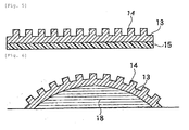
Fig. 3] Fig. 3 is a group of sectional views of amother mold 11 and a laminate 20 for forming depressions and protrusions by transferring fine depressions and protrusions from themother mold 11 tosilicone rubber 13 with asubstrate 11. - [
Fig. 4] Fig. 4 is a sectional view given when fine depressions and protrusions are transferred from themother mold 11 to thesilicone rubber 13 with asubstrate 11. - [
Fig. 5] Fig. 5 is a sectional view showing fine depressions and protrusions formed on thesilicone rubber 13 with asubstrate 11. - [
Fig. 6] Fig. 6 is a sectional view showing an example of a state where thesilicone rubber 13 has been allowed to adhere to a curved surface body. - Next, the present invention is described in more detail with reference to the examples of the present invention, but it should be construed that the present invention is in no way limited to those examples.
- The nanoimprint mold of the present invention is obtained by bringing a silicone rubber elastic body having an Hs rubber hardness of 10 to 55, preferably 20 to 40, into contact with a mother mold having fine depressions and protrusions formed thereon and carrying out thermal imprinting or photo imprinting (see
Fig. 3 to Fig. 5 ). InFig. 3 to Fig. 5 ,reference numeral 11 designates a mother mold, andreference numeral 13 designates uncured silicone rubber.Reference numeral 15 designates a substrate, and the substrate is preferably used to support the uncured silicone rubber. - The
mother mold 11 is not specifically restricted provided that it is a publicly known nanoimprint mold. The mother mold may be a mold prepared from silicone, glass, a metal or the like, or may be such a replica mold as described in Japanese Patent Laid-Open Publication No.2011-25677 - The resin used for the
substrate 15 is not specifically restricted, but in order to photo-cure the silicone rubber, a light transmitting resin is preferably used, and it is preferable to use polycarbonate (PC), polyethylene terephthalate (PET), polymethyl methacrylate (PMMA) or the like. Since the mold is used after thissubstrate 15 is peeled off, at least a surface of the substrate on which a silicone rubber layer is to be provided is preferably subj ected to release treatment. - On the surface of such a
substrate 15, an uncuredsilicone rubber layer 13 is formed. - This
silicone rubber layer 13 comprises a mixture of tetrafunctional, trifunctional, bifunctional or monofunctional organosiloxane and a catalyst, and the mixture is cured by means of light (ultraviolet light) or heat to form a ladder polymer, whereby silicone rubber having a specific Hs rubber hardness is formed. Especially in the present invention, it is preferable to adjust the type of the organosiloxane so that the silicone rubber, which is obtained by bringing the mixture into contact with the mother mold and subj ecting it to thermal imprinting or photo imprinting to transfer the depression-protrusion profile having been formed on the surface of the mother mold, as shown inFig. 4 , may have an Hs rubber hardness of 10 to 55, preferably 20 to 40. Before and after the curing, the thickness of the silicone rubber layer is 50 to 5000 µm, preferably 100 to 1000 µm. On the silicone rubber layer, a release layer can be further laminated. - The Hs rubber hardness in the present invention is a hardness derived from the following formula.
- [Math. 1]

- In this formula, G is a modulus of transverse elasticity (Pa) of the silicone elastic body after cured by heat or light, and G50 is a rubber constant of a rubber having a hardness of 50, and in the present invention, the rubber constant is 7.45×10⁵÷1.0197 (Pa) obtained based on the description of "Sesshoku ni yoru ouryoku no shuchu to gensui (concentration and decay of stress due to contact)" (Mech D&A News Letter, Vol. 1997-1, Mechanical Design Co., Ltd.). A specific method to measure the modulus of transverse elasticity is described later in the working examples.
- In
Fig. 5 , apattern 14 that is reverse to the pattern formed on themother mold 11 is formed on the surface of the silicon rubber layer having been cured by irradiating the silicone rubber layer with light. - By allowing this
reverse pattern 14 to adhere to a curved surface body such as a lens, preferably a curved surface body having a curved surface part having a curvature radius of not more than 500 mm, a nanoimprint mold of the present invention can be formed. - The nanoimprint mold of the present invention thus formed is preferably used for imprinting on a thermoplastic resin or a thermosetting resin. As the transfer material imprinted, not only such a conventional flat body (film) as nanoimprinted but also a fine curved surface body which has a curved surface part having a curvature radius of not more than 500 mm and has depressions and protrusions having an interval of 50 to 200000 nm, preferably 100 to 100000 nm, on the surface of the curved surface part can be prepared, because the nanoimprint mold of the present invention has proper morphological follow-up property and hardness. In the case where imprinting is made on a curved surface body, it is preferable to narrow the interval between protrusions of the depressions and protrusions formed on the surface of the mold more and more toward the peripheral part from the central part, according to the Hs rubber hardness of the silicone rubber elastic body, because the nanoimprint mold of the present invention extends.
- The silicone rubber for use in the present invention has good morphological follow-up property to a curved surface and can be brought into close contact with a curved surface of a curved surface body without any gap, because the Hs rubber hardness is in the above range.
- Next, the nanoimprint mold and the curved surface body of the present invention are further described with reference to the following examples, but it should be construed that the present invention is in no way limited to those examples.
- Various properties of the nanoimprint mold of the present invention can be measured by the use of the following apparatuses.
- Four kinds of sheets composed of uncured silicone rubber and having a thickness of 250 µm were prepared, and modulus of transverse elasticity and total light transmittance were measured in the following manner. Sample (rubber hardness : sample thickness)
- Using a rheometer (manufactured by Anton Paar, name of apparatus: PHYSICA MCR300), modulus of transverse elasticity was measured under the following conditions.
- Temperature control apparatus: TC30/CTD600
- Measuring fixture: PP8
- Number of points of measurement: 10 points
- Measuring interval: 10 sec
- Measuring time: 100 sec
- Measurement mode: rotation
- Strain (y): 0→0.1 (Linear)
- Normal force: 10 N
- Temperature: 23°C
- (Total light transmittance)
- Using a haze meter (manufactured by Murakami Color Research Laboratory Co., Ltd., type: HM-150), total light transmittance was measured in accordance with JIS K7105.
- [Table 1]
Table 1 Silicone rubber Modulus of transverse elasticity Hs rubber hardness Total light transmittance KE-103 240000 Pa 26 88% KE-106 730000 Pa 52 88% SIM-260 110000 Pa 62 88% KE-1204 140000 Pa 67 20% * The silicone rubbers are each manufactured by Shin-Etsu silicone Co., Ltd. - A glass substrate was coated with uncured silicone rubber (KE-103) by spin coating (rotation speed: 500 rpm, time: 20 sec) to prepare a resin layer. Against the laminate of the substrate and the resin layer, a master mold (quartz mold having been subjected to mold release treatment, transfer surface: 30 mm square, 150 nm L&S) was pressed, and a deposit of the resin layer was heated to 140°C to perform thermal curing transfer. During the thermal curing transfer, the pressing pressure was 1 MPa, and the holding time was 20 minutes. Thereafter, cooling was carried out, and the master mold was removed to obtain a silicone rubber mold having a thickness of 100 µm.
- On a surface of a curved surface lens having a curvature radius of 40 mm, a proper amount of an UV curable resin was dropped, and the silicone mold was pressed against the above lens surface so that the liquid dropped might spread over the whole surface, and the silicone mold was fixed thereto. Then, UV irradiation was carried out through the silicone mold to cure the UV curable resin, whereby the same profile as that of the master mold was transferred to the whole surface of the lens.
- A film master mold and uncured KE-103 were interposed between two glass substrates. When the uncured KE-103 spread over the whole surface of the film master mold, the glass substrates were fixed so as not to shift, and in such a fixed state, they were allowed to stand still in a drier having been adjusted to 150°C to cure the KE-103, whereby a silicone mold having a thickness of 1 mm was obtained.
- Transfer was carried out under the same conditions as in Example 1 to obtain a lens, to the whole surface of which the same profile as that of the master mold had been transferred.
- Using KE-106, a silicone mold was prepared in the same manner as in Example 2. Thus, a silicone mold having a thickness of 1 mm was obtained. Thereafter, transfer was carried out under the same conditions as those for the transfer to curved surface in Example 1, whereby a lens, to the whole surface of which the same profile as that of the master mold had been transferred, was obtained.
- Using SIM-260, a silicone mold was prepared in the same manner as in Example 2. Thus, a silicone mold having a thickness of 1 mm was obtained. Thereafter, transfer was carried out under the same conditions as those for the transfer to curved surface in Example 1. However, it was difficult to follow up the whole surface of the lens, and to the edges of the curved surface lens, the same profile as that of the master mold could not be transferred.
- Using KE-1204, a silicone mold was prepared in the same manner as in Example 2. Thus, a silicone mold having a thickness of 1 mm was obtained. Thereafter, transfer was carried out under the same conditions as those for the transfer to curved surface in Example 1. However, it was difficult to follow up the whole surface of the lens, and moreover, it was difficult to cure the UV curable resin because of low transparency.
-
Table 2 Silicone rubber Thickness Curvature radius Results of transfer Ex. 1 KE-103 100 µm 40 ○ Ex. 2 KE-103 1 mm 40 ○ Ex. 3 KE-106 1 mm 40 ○ Comp. Ex. 1 SIM-260 1 mm 40 Δ Comp. Ex. 2 KE-1204 1 mm 40 × - The nanoimprint molds obtained as above were each allowed to adhere to a surface of a spherical lens shown in
Fig. 1 to produce curved surface bodies. -
- 11:
- mother mold
- 13:
- thermoplastic resin
- 14:
- depressions and protrusions
- 15:
- substrate
- 18:
- curved surface body
- 20:
- laminate for forming depressions and protrusions
Claims (7)
- A nanoimprint mold comprising a silicone rubber elastic body having an Hs rubber hardness of 10 to 55, and having fine depressions and protrusions formed on the surface.
- The nanoimprint mold as claimed in claim 1, wherein the silicone rubber elastic body is ultraviolet curable silicone rubber or thermosetting silicone rubber.
- The nanoimprint mold as claimed in claim 1, wherein the total light transmittance of the silicone rubber (measured using a sheet having a thickness of 250 µm in accordance with JIS K7105) is not less than 60%.
- The nanoimprint mold as claimed in claim 1, wherein the silicone rubber elastic body is formed on a surface of a transparent substrate.
- The nanoimprint mold as claimed in claim 4, wherein the transparent substrate is a curved surface body having a curved surface part having a curvature radius of not more than 500 mm.
- A curved surface body having a curved surface part having a curvature radius of not more than 500 mm, and having depressions and protrusions having an interval of 50 to 100000 nm on the surface of the curved surface part.
- The curved surface body as claimed in claim 6, which is obtained by using the nanoimprint mold as claimed in any one of claims 1 to 5.
Applications Claiming Priority (2)
| Application Number | Priority Date | Filing Date | Title |
|---|---|---|---|
| JP2011112187 | 2011-05-19 | ||
| PCT/JP2012/062391 WO2012157636A1 (en) | 2011-05-19 | 2012-05-15 | Nanoimprint mold and curved body |
Publications (2)
| Publication Number | Publication Date |
|---|---|
| EP2711161A1 true EP2711161A1 (en) | 2014-03-26 |
| EP2711161A4 EP2711161A4 (en) | 2015-06-17 |
Family
ID=47176953
Family Applications (1)
| Application Number | Title | Priority Date | Filing Date |
|---|---|---|---|
| EP12785578.1A Withdrawn EP2711161A4 (en) | 2011-05-19 | 2012-05-15 | Nanoimprint mold and curved body |
Country Status (7)
| Country | Link |
|---|---|
| US (1) | US20140099474A1 (en) |
| EP (1) | EP2711161A4 (en) |
| JP (1) | JP5868393B2 (en) |
| KR (1) | KR20140010386A (en) |
| CN (1) | CN103429417A (en) |
| TW (1) | TW201300218A (en) |
| WO (1) | WO2012157636A1 (en) |
Cited By (4)
| Publication number | Priority date | Publication date | Assignee | Title |
|---|---|---|---|---|
| EP3456506A4 (en) * | 2016-05-09 | 2019-12-11 | Dexerials Corporation | REPLICA MASTER MOLD, METHOD OF MANUFACTURING REPLICA MASTER MOLD, ARTICLE AND METHOD OF MANUFACTURING BODY TO BE FORMED |
| EP3603922A4 (en) * | 2017-03-27 | 2020-11-18 | Daicel Corporation | SILICONE MOLD |
| CN111971590A (en) * | 2018-03-30 | 2020-11-20 | 迪睿合株式会社 | Resin laminated optical body and method for producing same |
| EP3988282A1 (en) * | 2016-05-09 | 2022-04-27 | Dexerials Corporation | Replica master mold and article |
Families Citing this family (7)
| Publication number | Priority date | Publication date | Assignee | Title |
|---|---|---|---|---|
| KR102143674B1 (en) * | 2013-11-29 | 2020-08-12 | 에베 그룹 에. 탈너 게엠베하 | Mould with a mould pattern, and method for producing same |
| JP6491928B2 (en) * | 2015-03-31 | 2019-03-27 | 株式会社協同インターナショナル | Replica mold and manufacturing method thereof |
| CN108008599B (en) * | 2017-12-27 | 2024-01-26 | 青岛天仁微纳科技有限责任公司 | Method and device for three-dimensional curved surface nanoscale imprinting and mold preparation method |
| KR102096606B1 (en) | 2018-08-29 | 2020-04-02 | 부산대학교 산학협력단 | Fabrication of nanoimprint soft mold for cylinder surface and nano-imprint process for cylindrical surface |
| EP3633453B1 (en) * | 2018-10-03 | 2023-12-27 | ZKW Group GmbH | Method for the preparation of (sub)-microstructures on curved surfaces of an optical component |
| KR102194832B1 (en) * | 2019-01-03 | 2020-12-23 | 부산대학교 산학협력단 | Method for Fabricating Nanostructured Surface on Curved Lens |
| JP7136831B2 (en) * | 2020-04-08 | 2022-09-13 | エーファウ・グループ・エー・タルナー・ゲーエムベーハー | STAMPER HAVING STAMPER STRUCTURE AND MANUFACTURING METHOD THEREOF |
Family Cites Families (24)
| Publication number | Priority date | Publication date | Assignee | Title |
|---|---|---|---|---|
| JPS60145846A (en) * | 1984-01-09 | 1985-08-01 | 凸版印刷株式会社 | Manufacture of polyester decorative board using silicon shaped film |
| JPS6189380A (en) * | 1984-10-08 | 1986-05-07 | Kyowa Leather Kk | Production of suede-like plastic sheet |
| FI901538A7 (en) * | 1990-03-28 | 1991-09-29 | Exel Oy | FOERFARANDE FOER FRAMSTAELLNING AV ETT SKAFT AV FIBERMATERIAL TILL EN GOLFCLUBBA OCH ETT SKAFT AV FIBERMATERIAL TILL EN GOLFKLUBBA. |
| US7070406B2 (en) * | 2003-04-29 | 2006-07-04 | Hewlett-Packard Development Company, L.P. | Apparatus for embossing a flexible substrate with a pattern carried by an optically transparent compliant media |
| JP2005193473A (en) * | 2004-01-06 | 2005-07-21 | Three M Innovative Properties Co | Transfer mold, its manufacturing method and fine structure manufacturing method |
| JP2006126568A (en) * | 2004-10-29 | 2006-05-18 | Fuji Xerox Co Ltd | Method for manufacturing polymer optical waveguide device |
| EP1669196B1 (en) * | 2004-12-10 | 2008-05-21 | ESSILOR INTERNATIONAL (Compagnie Générale d'Optique) | Stamp for patterning, method for manufacturing such stamp and method for manufacturing an object using the stamp. |
| CN100517064C (en) * | 2005-08-08 | 2009-07-22 | 西安交通大学 | Method for manufacturing special purpose ultrahigh smoothness flexible mold for large-area micro-imprinting |
| KR100831046B1 (en) | 2006-09-13 | 2008-05-21 | 삼성전자주식회사 | Nano imprint mold and its manufacturing method |
| US7891636B2 (en) * | 2007-08-27 | 2011-02-22 | 3M Innovative Properties Company | Silicone mold and use thereof |
| JP4815464B2 (en) * | 2008-03-31 | 2011-11-16 | 株式会社日立製作所 | Fine structure transfer stamper and fine structure transfer apparatus |
| JP5347617B2 (en) * | 2008-03-31 | 2013-11-20 | 東レ株式会社 | Manufacturing method and manufacturing apparatus of fine shape transfer sheet |
| JP2009279831A (en) | 2008-05-22 | 2009-12-03 | Fujifilm Corp | Curved member, manufacturing method of curved member and manufacturing method of die |
| JP5195074B2 (en) * | 2008-06-26 | 2013-05-08 | 大日本印刷株式会社 | Mold |
| US20100028604A1 (en) * | 2008-08-01 | 2010-02-04 | The Ohio State University | Hierarchical structures for superhydrophobic surfaces and methods of making |
| JP5617636B2 (en) * | 2008-09-22 | 2014-11-05 | コニカミノルタ株式会社 | Wafer lens manufacturing method |
| JP5282510B2 (en) * | 2008-09-29 | 2013-09-04 | 大日本印刷株式会社 | Manufacturing method of stamp for micro contact printing (μCP) |
| CN101477304B (en) * | 2008-11-04 | 2011-08-17 | 南京大学 | Stamping method for copying high-resolution nano-structure on complicated shape surface |
| JP2010120316A (en) * | 2008-11-21 | 2010-06-03 | Ricoh Co Ltd | Manufacturing apparatus and method for resin molded product, and optical element |
| JP4798468B2 (en) * | 2009-01-30 | 2011-10-19 | ソニー株式会社 | Lens manufacturing apparatus and lens manufacturing method |
| US20120126458A1 (en) * | 2009-05-26 | 2012-05-24 | King William P | Casting microstructures into stiff and durable materials from a flexible and reusable mold |
| US8992157B2 (en) * | 2009-05-28 | 2015-03-31 | Caterpillar Global Mining Llc | Hydraulic cylinder with guide bushing for a sliding dipper handle of a power shovel |
| JP5403371B2 (en) | 2009-06-22 | 2014-01-29 | 綜研化学株式会社 | Method for producing metal mold and resin mold and resin for producing the metal mold |
| JP5531463B2 (en) * | 2009-06-26 | 2014-06-25 | 大日本印刷株式会社 | Master plate used for manufacturing micro contact print stamps and manufacturing method thereof, micro contact printing stamp and manufacturing method thereof, and pattern forming method using micro contact printing stamp |
-
2012
- 2012-05-15 WO PCT/JP2012/062391 patent/WO2012157636A1/en not_active Ceased
- 2012-05-15 EP EP12785578.1A patent/EP2711161A4/en not_active Withdrawn
- 2012-05-15 CN CN2012800141418A patent/CN103429417A/en active Pending
- 2012-05-15 JP JP2013515161A patent/JP5868393B2/en not_active Expired - Fee Related
- 2012-05-15 US US14/118,360 patent/US20140099474A1/en not_active Abandoned
- 2012-05-15 KR KR20137022137A patent/KR20140010386A/en not_active Withdrawn
- 2012-05-17 TW TW101117529A patent/TW201300218A/en unknown
Cited By (9)
| Publication number | Priority date | Publication date | Assignee | Title |
|---|---|---|---|---|
| EP3456506A4 (en) * | 2016-05-09 | 2019-12-11 | Dexerials Corporation | REPLICA MASTER MOLD, METHOD OF MANUFACTURING REPLICA MASTER MOLD, ARTICLE AND METHOD OF MANUFACTURING BODY TO BE FORMED |
| EP3988282A1 (en) * | 2016-05-09 | 2022-04-27 | Dexerials Corporation | Replica master mold and article |
| US12076890B2 (en) | 2016-05-09 | 2024-09-03 | Dexerials Corporation | Replica master mold, method of manufacturing replica master mold, article, and method of manufacturing formation object |
| EP3603922A4 (en) * | 2017-03-27 | 2020-11-18 | Daicel Corporation | SILICONE MOLD |
| US11247368B2 (en) | 2017-03-27 | 2022-02-15 | Daicel Corporation | Silicone mold |
| CN111971590A (en) * | 2018-03-30 | 2020-11-20 | 迪睿合株式会社 | Resin laminated optical body and method for producing same |
| EP3757627A4 (en) * | 2018-03-30 | 2021-11-03 | Dexerials Corporation | OPTICAL BODY STACKED IN RESIN AND ASSOCIATED MANUFACTURING PROCESS |
| CN111971590B (en) * | 2018-03-30 | 2023-03-10 | 迪睿合株式会社 | Resin laminated optical body and method for producing same |
| US11897182B2 (en) | 2018-03-30 | 2024-02-13 | Dexerials Corporation | Resin laminated optical body and method for manufacturing the same |
Also Published As
| Publication number | Publication date |
|---|---|
| TW201300218A (en) | 2013-01-01 |
| JP5868393B2 (en) | 2016-02-24 |
| JPWO2012157636A1 (en) | 2014-07-31 |
| CN103429417A (en) | 2013-12-04 |
| KR20140010386A (en) | 2014-01-24 |
| EP2711161A4 (en) | 2015-06-17 |
| US20140099474A1 (en) | 2014-04-10 |
| WO2012157636A1 (en) | 2012-11-22 |
Similar Documents
| Publication | Publication Date | Title |
|---|---|---|
| US20140099474A1 (en) | Nanoimprint Mold and Curved Surface Body | |
| KR101381489B1 (en) | Resin mold | |
| KR100314563B1 (en) | Pressure Sensitive Adhesive with Microstructured Surface | |
| US20130011608A1 (en) | Optical films with microstructured low refractive index nanovoided layers and methods therefor | |
| TWI394660B (en) | Thin film laminate and method of manufacturing same | |
| EP2602088B1 (en) | Resin mold for nanoimprinting | |
| RU2695290C2 (en) | Method of making die with pattern, die with pattern and method for printing | |
| JPWO2009041646A1 (en) | Photocurable composition, method for producing fine pattern formed body, and optical element | |
| WO2009032815A1 (en) | Tool for making microstructured articles | |
| US20100052216A1 (en) | Nano imprint lithography using an elastic roller | |
| EP3615598B1 (en) | Transparent composite film with hard coating, method for forming the same and flexible display device including the same | |
| TWI665078B (en) | Method of manufacturing patterned stamp forpatterning contoured surface, patterned stampfor use in imprint lithography process, imprint lithography method, article comprising patterned contoured surface and use of a patterned stamp for imprint lithograph | |
| JP7637816B2 (en) | Method and apparatus for removing stamp | |
| US10155340B2 (en) | Mold, method for producing mold, and method for producing nanoimprint film | |
| JP2007245702A (en) | Template and method for producing treated substrate having transferred fine pattern | |
| CN110764366A (en) | Stamp having stamp structure and method of manufacturing the same | |
| CN105731365A (en) | PDMS elastomer micro-nano processing method based on crosslinking control control transfer printing | |
| KR101373362B1 (en) | Apparatus for manufacturing a nano pattern structure | |
| KR20200058096A (en) | The monolithic structure of Patterned Release film, Method of producing the same and Adhesive tape produced from the same | |
| CN103129201B (en) | Transfer sheet for transfer and manufacturing method thereof | |
| WO2014163041A1 (en) | Transfer film and substrate with relief structure | |
| KR102289836B1 (en) | Method for producing (sub)microstructures on curved surfaces of an optical component, and optical component | |
| JP2014210362A (en) | Blanket for offset printing, and method for producing the blanket | |
| JP6844010B2 (en) | Electroforming master and method for manufacturing electroformed molds using the electroforming master | |
| CN100575036C (en) | Manufacturing method of mold and base material with transferred fine pattern |
Legal Events
| Date | Code | Title | Description |
|---|---|---|---|
| PUAI | Public reference made under article 153(3) epc to a published international application that has entered the european phase |
Free format text: ORIGINAL CODE: 0009012 |
|
| 17P | Request for examination filed |
Effective date: 20130919 |
|
| AK | Designated contracting states |
Kind code of ref document: A1 Designated state(s): AL AT BE BG CH CY CZ DE DK EE ES FI FR GB GR HR HU IE IS IT LI LT LU LV MC MK MT NL NO PL PT RO RS SE SI SK SM TR |
|
| DAX | Request for extension of the european patent (deleted) | ||
| RIC1 | Information provided on ipc code assigned before grant |
Ipc: H01L 21/027 20060101ALI20150218BHEP Ipc: B29C 59/02 20060101AFI20150218BHEP Ipc: B29C 33/40 20060101ALI20150218BHEP |
|
| RA4 | Supplementary search report drawn up and despatched (corrected) |
Effective date: 20150518 |
|
| RIC1 | Information provided on ipc code assigned before grant |
Ipc: B29C 33/40 20060101ALI20150511BHEP Ipc: H01L 21/027 20060101ALI20150511BHEP Ipc: B29C 59/02 20060101AFI20150511BHEP |
|
| STAA | Information on the status of an ep patent application or granted ep patent |
Free format text: STATUS: THE APPLICATION HAS BEEN WITHDRAWN |
|
| 18W | Application withdrawn |
Effective date: 20151112 |