EP2710735B1 - Compensated current cell to scale switching glitches in digital to analog convertors - Google Patents
Compensated current cell to scale switching glitches in digital to analog convertors Download PDFInfo
- Publication number
- EP2710735B1 EP2710735B1 EP12726952.0A EP12726952A EP2710735B1 EP 2710735 B1 EP2710735 B1 EP 2710735B1 EP 12726952 A EP12726952 A EP 12726952A EP 2710735 B1 EP2710735 B1 EP 2710735B1
- Authority
- EP
- European Patent Office
- Prior art keywords
- current
- compensation
- switching
- cell
- output
- Prior art date
- Legal status (The legal status is an assumption and is not a legal conclusion. Google has not performed a legal analysis and makes no representation as to the accuracy of the status listed.)
- Not-in-force
Links
- 230000004044 response Effects 0.000 claims description 6
- XAUDJQYHKZQPEU-KVQBGUIXSA-N 5-aza-2'-deoxycytidine Chemical compound O=C1N=C(N)N=CN1[C@@H]1O[C@H](CO)[C@@H](O)C1 XAUDJQYHKZQPEU-KVQBGUIXSA-N 0.000 description 16
- 238000005516 engineering process Methods 0.000 description 6
- 238000013461 design Methods 0.000 description 5
- 230000006870 function Effects 0.000 description 4
- 238000006243 chemical reaction Methods 0.000 description 3
- 230000000295 complement effect Effects 0.000 description 3
- 230000008878 coupling Effects 0.000 description 3
- 238000010168 coupling process Methods 0.000 description 3
- 238000005859 coupling reaction Methods 0.000 description 3
- 238000002347 injection Methods 0.000 description 3
- 239000007924 injection Substances 0.000 description 3
- 238000000034 method Methods 0.000 description 3
- 230000003287 optical effect Effects 0.000 description 3
- 230000009467 reduction Effects 0.000 description 3
- 239000000835 fiber Substances 0.000 description 2
- PUPNJSIFIXXJCH-UHFFFAOYSA-N n-(4-hydroxyphenyl)-2-(1,1,3-trioxo-1,2-benzothiazol-2-yl)acetamide Chemical compound C1=CC(O)=CC=C1NC(=O)CN1S(=O)(=O)C2=CC=CC=C2C1=O PUPNJSIFIXXJCH-UHFFFAOYSA-N 0.000 description 2
- 230000003071 parasitic effect Effects 0.000 description 2
- 239000002245 particle Substances 0.000 description 2
- 239000000243 solution Substances 0.000 description 2
- 230000005540 biological transmission Effects 0.000 description 1
- 239000003990 capacitor Substances 0.000 description 1
- 230000008859 change Effects 0.000 description 1
- 238000004891 communication Methods 0.000 description 1
- 239000002131 composite material Substances 0.000 description 1
- 238000004590 computer program Methods 0.000 description 1
- 239000013256 coordination polymer Substances 0.000 description 1
- 238000010586 diagram Methods 0.000 description 1
- 238000012986 modification Methods 0.000 description 1
- 230000004048 modification Effects 0.000 description 1
- 238000004513 sizing Methods 0.000 description 1
- 238000012546 transfer Methods 0.000 description 1
Images

Classifications
-
- H—ELECTRICITY
- H03—ELECTRONIC CIRCUITRY
- H03K—PULSE TECHNIQUE
- H03K17/00—Electronic switching or gating, i.e. not by contact-making and –breaking
- H03K17/16—Modifications for eliminating interference voltages or currents
- H03K17/161—Modifications for eliminating interference voltages or currents in field-effect transistor switches
- H03K17/162—Modifications for eliminating interference voltages or currents in field-effect transistor switches without feedback from the output circuit to the control circuit
-
- H—ELECTRICITY
- H03—ELECTRONIC CIRCUITRY
- H03M—CODING; DECODING; CODE CONVERSION IN GENERAL
- H03M1/00—Analogue/digital conversion; Digital/analogue conversion
- H03M1/06—Continuously compensating for, or preventing, undesired influence of physical parameters
- H03M1/08—Continuously compensating for, or preventing, undesired influence of physical parameters of noise
- H03M1/0863—Continuously compensating for, or preventing, undesired influence of physical parameters of noise of switching transients, e.g. glitches
-
- H—ELECTRICITY
- H03—ELECTRONIC CIRCUITRY
- H03M—CODING; DECODING; CODE CONVERSION IN GENERAL
- H03M1/00—Analogue/digital conversion; Digital/analogue conversion
- H03M1/66—Digital/analogue converters
- H03M1/74—Simultaneous conversion
- H03M1/742—Simultaneous conversion using current sources as quantisation value generators
Definitions
- the present application relates generally to the operation and design of RF systems, and more particularly, to digital to analog convertors.
- Digital to analog convertors are used in a variety of applications, such as in transmitters, to convert digital data into an analog signal for transmission.
- One type of DAC is referred to as a current steering DAC and operates to convert digital data into a corresponding current that can be used to generate an analog voltage signal representative of the digital data.
- a current steering DAC switches current at its output based on a digital input so that adjacent current levels differs by an amount corresponding to a least significant bit (LSB).
- LSB least significant bit
- a 14-bit DAC can output up to 16,384 different current levels.
- switching transients When a current steering DAC changes state, switching transients (or glitches) are generated which can degrade the DAC's performance. For example, glitches may cause inaccuracies during the conversion of the current output to an analog voltage. Since switching transients are unavoidable, it is desirable that they be identical to minimize their impact on DAC performance.
- One way to have identical switching transients is to design the DAC (i.e., 14-bit DAC in this example) with 16,383 individual current sources that are selectively enabled based on the digital code to be converted. Although this solution may assure identical glitches, implementing such a large number of current sources is not very efficient.
- Another alternative would be to design the DAC with binary weighted current sources. Thus, for a 14-bit DAC, there will be fourteen individually controllable current sources that differ in weight by a factor of two from one source to the next.
- binary weighted current sources can be difficult to produce so that the current matching requirements are accurately met. Additionally, binary weighted current sources will not be able to easily scale the glitches that they generate.
- US 2006/125670 discloses a current cell including a current source; a first transistor transmitting a current produced from the current source to a first output node based on a first signal; a second transistor transmitting a current produced from the current source to a second output node based on a second signal.
- US 2002/030621 discloses a digital/analog converter comprising a plurality of current sources, and a selecting circuit for selecting a current source from the plurality of current sources on the basis of a digital signal.
- FIG. 1 shows a conventional uncompensated current cell 100 for use in a current steering DAC.
- the current cell 100 comprises a differential PMOS transistor pair (M1, M1b) connected to receive current (10) from a current source 102.
- Complementary signal inputs Y and Yb control the transistors M1 and M1b, respectively, to switch the current (10) to generate complementary output currents ioutm and ioutp.
- VM and VP represent low impedance sources which receive the currents ioutm and ioutp.
- the currents ioutm and ioutp are converted to voltages elsewhere in the DAC circuit.
- the capacitors C1, C2, C1b and C2b are the parasitic capacitances associated with the devices M1 and M1b and contribute to the glitches generated by the switching of the current cell 100.
- the current cell 100 During operation, the current cell 100 generates switching glitches that result from switching the differential transistor pair in response to the differential inputs Y and Yb.
- the resulting glitches have at least the following two sources.
- Clock feed-through is the result of a clock signal (or in this case the differential inputs Y and Yb) capacitively coupling into the output.
- the inputs Y and Yb of each current cell will couple into the shared outputs ioutm and ioutp through the parasitic capacitances associated with the differential switch.
- the clock signal is configured to drive a DAC comprising a plurality of the current cells 100 to convert a digital input to a current output.
- Charge injection is the result of channel charge associated with the transistors (M1, M1b) coupling to the output current when the transistors change state. A more detailed description of how switching glitches are generated is provided below.
- FIG. 2 shows a conventional graph 200 illustrating glitches generated during operation of the uncompensated current cell 100 shown in FIG. 1 .
- the graph 200 shows a plot of the differential input signals Y and Yb that switch the differential pair M1 and M1b.
- a plot of the output currents ioutm and ioutp that result from the operation of the differential pair M1 and M1b is also shown.
- the current 10 is switched from producing ioutm to producing ioutp.
- glitches 202 , 204 and 206 occur as shown in plot of the currents ioutm and ioutp.
- Glitch 202 is produced as a result of coupling from M1b "turn on" charge injection.
- Glitch 204 is produced when M1 turns off, and glitch 206 is produced when M1b turns on.
- the three glitches 202 , 204 , and 206 will combine to create a single composite glitch that may result in degraded DAC performance.
- a novel compensated current cell that operates to scale glitches in a current steering DAC.
- the compensated current cell comprises two compensation devices that generate compensation currents used to scale the glitches.
- the compensated current cell is used to convert the least significant bits of a digital value, and as a result, switching glitches at the DAC output can be accurately scaled.
- the compensated current cell is used to convert the entire digital value, and as a result, switching glitches at the DAC output can be significantly reduced or eliminated.
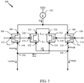
- FIG. 3 shows an exemplary compensated current cell 300.
- the compensated current cell 300 is suitable for use to scale, reduce or eliminate switching glitches in a current switching DAC.
- the current cell 300 comprises a current source 302 connected to provide an input current 10 to source terminals 304 and 306 of differential PMOS transistor pair 308 and 310 , respectively.
- the transistors 308 and 310 are connected to complementary input signals (Z and Zb) at their gate terminals 312 and 314 , respectively.
- the input signals (Z and Zb) operate to switch the transistors 308 and 310 on and off so as to switch the input current 10 to drain terminals 316 and 318 ; thereby producing output currents ioutm and ioutp, respectively.
- the current cell 300 also comprises compensation PMOS transistors 320 and 322 .
- the compensation transistors 320 and 322 have their respective source terminals 324 and 326 connected together.
- the input signal Z is connected to gate terminal 328 of compensation transistor 320
- the input signal Zb is connected to gate terminal 330 of compensation transistor 322 .
- the input signals (Z and Zb) operate to switch the compensation transistors 320 and 322 on and off to produce compensation currents ipc and imc at drain terminals 332 and 334 , respectively.
- all devices operate in triode mode.
- the drain terminals 316 and 318 provide the output currents ioutm and ioutp, respectively.
- the compensation currents imc and ipc are coupled to the signal paths carrying the output currents ioutm and ioutp at terminals 336 and 338 , respectively. Glitch scaling is provided when the compensation currents imc and ipc combine with the output currents ioutm and ioutp to produce compensated output currents ioutmc and ioutmp.
- the compensation currents cancel out (or scale) a predetermined portion of the glitch that would normally appear in an uncompensated current cell, for instance, the uncompensated current cell 100 shown in FIG. 1 .
- the scaling of the glitch is determined by the size difference between the current switches 308 and 310 and their associated compensation devices 322 and 320.
- the current switch 308 has device size S SM and the current switch 310 has device size S SP .
- the compensation device 320 has device size S CP and the compensation device 322 has device size S CM .
- the difference in size between (S SM and S CM ) and (S SP and S CP ) determines the amount of glitch scaling.
- the difference in size between (S SM and S CM ) is the same as the difference in size between (S SP and S CP ). However, in other implementations, these size differences may not be identical.
- the size difference is determined by the difference in channel widths (W0) between the devices.
- W0 channel widths
- the current produced by the current cells are scaled using various techniques. For example, in a conventional 14-bit DAC, the ratio of the current associated with the MSB current cell to the current associated with the LSB current cell is 2 14 :1 or 16384:1. Such a high ratio may be difficult to implement accurately, therefore, segmented architectures are frequently used in DAC designs. In this exemplary implementation, a segmented architecture is used to set the ratio between the largest and smallest currents switched by the current cells of the DAC 400 to 256:1.
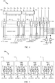
- the DAC 400 has a segmented architecture that comprises a first thermometer decoder 402 that is configured for (6 to 63) decoding.
- the decoder 402 is connected to the most significant six bits (B 8 -B 13 ) of the 14-bit value to be converted, and decodes these bits to 63 signals that are connected to 63 uncompensated current cells 404 in an MSB portion of the DAC 400.
- the 63 signals comprise differential signals that are connected to the inputs of the uncompensated current cells 404.
- Each of the uncompensated current cells 404 switches current having a level of (16*I0).
- each of the uncompensated current cells comprises 16 switching devices connected together in parallel with each device switching a current level of I0 to produce the positive current output (ioutp) equal to (16*I0), and 16 switching devices connected together in parallel with each switching device switching a current level of I0 to produce the negative output current (ioutm) equal to (16*I0).
- the DAC 400 also comprises a second thermometer decoder 406 that is configured for (4 to 15) decoding.
- the decoder 406 is connected to the middle significant four bits (B 4 -B 7 ) of the 14-bit value to be converted, and decodes these bits to 15 signals that are connected to 15 uncompensated current cells 408 in a MID portion of the DAC 400.
- the 15 signals comprise differential signals that are connected to the inputs of the uncompensated current cells 408.
- Each of the uncompensated current cells 408 switches current having a level of (I0).
- each of the uncompensated current cells comprises 1 switching device switching a current level of I0 to produce the positive current output (ioutp) and 1 switching device switching a current level of I0 to produce the negative current output (ioutm).
- the DAC 400 also comprises four binary weighted compensated current cells 410 that are connected to the least significant four bits (B 0 -B 3 ) of the 14-bit value to be converted.
- each of the compensated current cells 410 may be the compensated current cell 300 shown in FIG. 3 .
- the bits (B 0 -B 3 ) comprise differential input signals that are connected to the inputs of the compensated current cells 410 to produce a 4-bit binary weighted compensated current output in an LSB portion of the DAC 400.
- each of the compensated current cells 410 switches current having a different scaled level of the current I0.
- the compensated current cell L1 switches a current having a scaled level of (I0/16), the current cell L2, switches a current having a scaled level of (I0/8), the current cell L3 switches a current having a scaled level of (I0/4), and the current cell L4 switches a current having a scaled level of (I0/2). Therefore, a current cell in the MSB portion of the DAC 400 switches a current that is represented by (I0*16) and the LSB current cell switches a current represented by (I0/16), which provides a ratio of 256:1. However, the current associated with the most significant bit (B 13 ) is actually the sum of the currents output from 32 current cells in the MSB portion, which is equivalent to (512*I0).
- All of the positive and minus currents are connected to output devices 414 and 412, respectively, which represent low impedance sources.
- the current in VP and VM is then converted to output voltages, VOUTP and VOUTM, elsewhere in the DAC 400. Because the DAC 400 utilizes the compensated current cell 410 to convert the least significant four bits of the digital value, the DAC 400 operates to provide scaled switching glitches and improved performance.
- the MID current cells 408 use minimum sized PMOS devices for their differential current switches to switch the input current I0 as described above. Since the current cells of the MSB portion of the DAC switch current that is 16 times larger than I0, the current cells in the MSB portion of the DAC (i.e., current cells 404 ) each use 16 minimum sized PMOS devices connected together in parallel for their current switching components. The current switches in the LSB current cells cannot be scaled below the minimum sized PMOS device, however, each of the compensated current cells 410 uses the size difference between their switching devices and their compensation devices to scale the switching glitches associated with these LSB cells.
- FIG. 5 shows four exemplary compensated current cells (L1-L4) used in the DAC 400 shown in FIG. 4 .
- each of the current cells (L1-L4) may be the current cell 300 shown in FIG. 3 .
- the current cells (L1-L4) represent the LSB binary weighted current cells 410 used to convert the four least significant bits of the 14-bit digital value shown in FIG. 4 .
- the current cells include switching devices and compensation devices that are appropriately sized to provide glitch scaling as described herein.
- device sizes are determined according to the following algorithm.
- Current scale factor size of switching device ⁇ size of comp . device
- the size of the p-side switching device is determined, but it is assumed that the size m-side switching devices are identically sized.
- the p-side switching device width is S SP1 and its compensation device width is S CP1 .
- the p-side switching device width is S SP2 and its compensation device width is S CP2 .
- the p-side switching device width is S SP3 and its compensation device width is S CP3 .
- the p-side switching device width is S SP4 and its compensation device width is S CP4 .
- a DAC can be configured with the compensated current cell to scale or reduce switching glitches for the entire DAC.
- all of the current cells of the DAC are implemented with the compensated current cell 300. This results in switching glitches being reduced throughout the DAC output range.
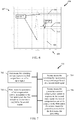
- the scaled glitch ( 610 , 612 ) associated with the compensated current cell is much smaller than the glitch ( 606 , 608 ) associated with the uncompensated current cell.
- the apparatus 700 comprises a first module comprising a first means ( 702 ) for switching an input current to a first output based on a first input signal, which in an aspect comprises device 308.
- the apparatus 700 comprises a second module comprising a second means ( 704 ) for switching the input current to a second output based on a second input signal, which in an aspect comprises device 310.
- the apparatus 700 also comprises a third module comprising a first means ( 706 ) for generating a first compensation current in response to the first input signal, the first compensation current is coupled to the second output, which in an aspect comprises device 320.
- the apparatus 700 also comprises a fourth module comprising a second means ( 708 ) for generating a second compensation current in response to the second input signal, the second compensation current is coupled to the first output, the second means for generating connected to the first means for generating, which in an aspect comprises device 322.
- a processor may also be implemented as a combination of computing devices, e.g., a combination of a DSP and a microprocessor, a plurality of microprocessors, one or more microprocessors in conjunction with a DSP core, or any other such configuration.
- a software module may reside in Random Access Memory (RAM), flash memory, Read Only Memory (ROM), Electrically Programmable ROM (EPROM), Electrically Erasable Programmable ROM (EEPROM), registers, hard disk, a removable disk, a CD-ROM, or any other form of storage medium known in the art.
- An exemplary storage medium is coupled to the processor such that the processor can read information from, and write information to, the storage medium.
- the storage medium may be integral to the processor.
- the processor and the storage medium may reside in an ASIC.
- the ASIC may reside in a user terminal.
- the processor and the storage medium may reside as discrete components in a user terminal.
- the functions described may be implemented in hardware, software, firmware, or any combination thereof. If implemented in software, the functions may be stored on or transmitted over as one or more instructions or code on a computer-readable medium.
- Computer-readable media includes both non-transitory computer storage media and communication media including any medium that facilitates transfer of a computer program from one place to another.
- a non-transitory storage media may be any available media that can be accessed by a computer.
- such computer-readable media can comprise RAM, ROM, EEPROM, CD-ROM or other optical disk storage, magnetic disk storage or other magnetic storage devices, or any other medium that can be used to carry or store desired program code in the form of instructions or data structures and that can be accessed by a computer.
- any connection is properly termed a computer-readable medium.
- the software is transmitted from a website, server, or other remote source using a coaxial cable, fiber optic cable, twisted pair, digital subscriber line (DSL), or wireless technologies such as infrared, radio, and microwave
- the coaxial cable, fiber optic cable, twisted pair, DSL, or wireless technologies such as infrared, radio, and microwave are included in the definition of medium.
- Disk and disc includes compact disc (CD), laser disc, optical disc, digital versatile disc (DVD), floppy disk and blu-ray disc where disks usually reproduce data magnetically, while discs reproduce data optically with lasers. Combinations of the above should also be included within the scope of computer-readable media.
Landscapes
- Engineering & Computer Science (AREA)
- Theoretical Computer Science (AREA)
- Analogue/Digital Conversion (AREA)
- Electronic Switches (AREA)
Description
- The present application relates generally to the operation and design of RF systems, and more particularly, to digital to analog convertors.
- Digital to analog convertors (DACs) are used in a variety of applications, such as in transmitters, to convert digital data into an analog signal for transmission. One type of DAC is referred to as a current steering DAC and operates to convert digital data into a corresponding current that can be used to generate an analog voltage signal representative of the digital data. For example, a current steering DAC switches current at its output based on a digital input so that adjacent current levels differs by an amount corresponding to a least significant bit (LSB). As a result, a 14-bit DAC can output up to 16,384 different current levels.
- When a current steering DAC changes state, switching transients (or glitches) are generated which can degrade the DAC's performance. For example, glitches may cause inaccuracies during the conversion of the current output to an analog voltage. Since switching transients are unavoidable, it is desirable that they be identical to minimize their impact on DAC performance.
- One way to have identical switching transients is to design the DAC (i.e., 14-bit DAC in this example) with 16,383 individual current sources that are selectively enabled based on the digital code to be converted. Although this solution may assure identical glitches, implementing such a large number of current sources is not very efficient. Another alternative would be to design the DAC with binary weighted current sources. Thus, for a 14-bit DAC, there will be fourteen individually controllable current sources that differ in weight by a factor of two from one source to the next. However, the problem with this solution is that binary weighted current sources can be difficult to produce so that the current matching requirements are accurately met. Additionally, binary weighted current sources will not be able to easily scale the glitches that they generate.
- Therefore, it would be desirable to have a DAC that allows switching transients to be controlled so that they scale in the same manner as the switching currents and therefore do not degrade DAC performance.
US 2006/125670 discloses a current cell including a current source; a first transistor transmitting a current produced from the current source to a first output node based on a first signal; a second transistor transmitting a current produced from the current source to a second output node based on a second signal.US 2002/030621 discloses a digital/analog converter comprising a plurality of current sources, and a selecting circuit for selecting a current source from the plurality of current sources on the basis of a digital signal. - The foregoing aspects described herein will become more readily apparent by reference to the following description when taken in conjunction with the accompanying drawings wherein:
-
FIG. 1 shows a conventional uncompensated current cell for use in a current steering DAC; -
FIG. 2 shows a conventional graph illustrating glitches generated during operation of the current cell shown inFIG. 1 ; -
FIG. 3 shows an exemplary compensated current cell; -
FIG. 4 shows an exemplary segmented current steering DAC comprising the compensated current cell shown inFIG. 3 ; -
FIG. 5 shows four exemplary compensated current cells representing four least significant bits of the DAC shown inFIG. 4 ; -
FIG. 6 shows an exemplary graph illustrating glitch reduction achieved with the compensated current cell shown inFIG. 3 ; and -
FIG. 7 shows an exemplary compensated current cell apparatus. - The detailed description set forth below in connection with the appended drawings is intended as a description of exemplary embodiments of the invention and is not intended to represent the only embodiments in which the invention can be practiced. The term "exemplary" used throughout this description means "serving as an example, instance, or illustration," and should not necessarily be construed as preferred or advantageous over other exemplary embodiments. The detailed description includes specific details for the purpose of providing a thorough understanding of the exemplary embodiments of the invention. It will be apparent to those skilled in the art that the exemplary embodiments of the invention may be practiced without these specific
details. In some instances, well known structures and devices are shown in block diagram form in order to avoid obscuring the novelty of the exemplary embodiments presented herein. -
FIG. 1 shows a conventional uncompensatedcurrent cell 100 for use in a current steering DAC. Thecurrent cell 100 comprises a differential PMOS transistor pair (M1, M1b) connected to receive current (10) from acurrent source 102. Complementary signal inputs Y and Yb control the transistors M1 and M1b, respectively, to switch the current (10) to generate complementary output currents ioutm and ioutp. VM and VP represent low impedance sources which receive the currents ioutm and ioutp. The currents ioutm and ioutp are converted to voltages elsewhere in the DAC circuit. The capacitors C1, C2, C1b and C2b are the parasitic capacitances associated with the devices M1 and M1b and contribute to the glitches generated by the switching of thecurrent cell 100. - During operation, the
current cell 100 generates switching glitches that result from switching the differential transistor pair in response to the differential inputs Y and Yb. The resulting glitches have at least the following two sources. - 1. clock feed-through
- 2. charge injection
- Clock feed-through is the result of a clock signal (or in this case the differential inputs Y and Yb) capacitively coupling into the output. In the case of the DAC, the inputs Y and Yb of each current cell will couple into the shared outputs ioutm and ioutp through the parasitic capacitances associated with the differential switch. For example, the clock signal is configured to drive a DAC comprising a plurality of the
current cells 100 to convert a digital input to a current output. Charge injection is the result of channel charge associated with the transistors (M1, M1b) coupling to the output current when the transistors change state. A more detailed description of how switching glitches are generated is provided below. -
FIG. 2 shows aconventional graph 200 illustrating glitches generated during operation of the uncompensatedcurrent cell 100 shown inFIG. 1 . For example, thegraph 200 shows a plot of the differential input signals Y and Yb that switch the differential pair M1 and M1b. A plot of the output currents ioutm and ioutp that result from the operation of the differential pair M1 and M1b is also shown. - As the transistor M1 turns off and the transistor M1b turns on in response to the inputs Y and Yb, the current 10 is switched from producing ioutm to producing ioutp. During this switch,
glitches glitch 206 is produced when M1b turns on. The threeglitches - A novel compensated current cell is disclosed that operates to scale glitches in a current steering DAC. The compensated current cell comprises two compensation devices that generate compensation currents used to scale the glitches. In one exemplary DAC implementation, the compensated current cell is used to convert the least significant bits of a digital value, and as a result, switching glitches at the DAC output can be accurately scaled. In another exemplary DAC implementation, the compensated current cell is used to convert the entire digital value, and as a result, switching glitches at the DAC output can be significantly reduced or eliminated.
-
FIG. 3 shows an exemplary compensatedcurrent cell 300. For example, the compensatedcurrent cell 300 is suitable for use to scale, reduce or eliminate switching glitches in a current switching DAC. - The
current cell 300 comprises acurrent source 302 connected to provide an input current 10 to sourceterminals PMOS transistor pair transistors gate terminals transistors terminals - The
current cell 300 also comprisescompensation PMOS transistors compensation transistors respective source terminals gate terminal 328 ofcompensation transistor 320, and the input signal Zb is connected togate terminal 330 ofcompensation transistor 322. The input signals (Z and Zb) operate to switch thecompensation transistors drain terminals - The
drain terminals terminals - The compensation currents cancel out (or scale) a predetermined portion of the glitch that would normally appear in an uncompensated current cell, for instance, the uncompensated
current cell 100 shown inFIG. 1 . The scaling of the glitch is determined by the size difference between thecurrent switches compensation devices current switch 308 has device size SSM and thecurrent switch 310 has device size SSP. In addition, thecompensation device 320 has device size SCP and thecompensation device 322 has device size SCM. Thus, the difference in size between (SSM and SCM) and (SSP and SCP) determines the amount of glitch scaling. In one implementation, the difference in size between (SSM and SCM) is the same as the difference in size between (SSP and SCP). However, in other implementations, these size differences may not be identical. - Assuming the channel lengths of the switching (308, 310) and compensation (320, 322) devices are the same, the size difference is determined by the difference in channel widths (W0) between the devices. A more detailed description of how the size difference between the current switches devices and their associated compensation devices is adjusted for glitch scaling is provided below.
-
FIG. 4 shows an exemplary segmentedcurrent steering DAC 400 comprising the compensatedcurrent cell 300 shown inFIG. 3 . For example, the compensatedcurrent cell 300 is configured to generate compensated output currents for each of the four least significant bits (LSBs) of theDAC 400. In this example, theDAC 400 is configured to convert a 14-bit digital value to an output current that is then converted to an analog voltage. - In DAC architectures, the current produced by the current cells are scaled using various techniques. For example, in a conventional 14-bit DAC, the ratio of the current associated with the MSB current cell to the current associated with the LSB current cell is 214:1 or 16384:1. Such a high ratio may be difficult to implement accurately, therefore, segmented architectures are frequently used in DAC designs. In this exemplary implementation, a segmented architecture is used to set the ratio between the largest and smallest currents switched by the current cells of the
DAC 400 to 256:1. - The
DAC 400 has a segmented architecture that comprises afirst thermometer decoder 402 that is configured for (6 to 63) decoding. Thedecoder 402 is connected to the most significant six bits (B8-B13) of the 14-bit value to be converted, and decodes these bits to 63 signals that are connected to 63 uncompensatedcurrent cells 404 in an MSB portion of theDAC 400. The 63 signals comprise differential signals that are connected to the inputs of the uncompensatedcurrent cells 404. Each of the uncompensatedcurrent cells 404 switches current having a level of (16*I0). For example, in one exemplary implementation, each of the uncompensated current cells comprises 16 switching devices connected together in parallel with each device switching a current level of I0 to produce the positive current output (ioutp) equal to (16*I0), and 16 switching devices connected together in parallel with each switching device switching a current level of I0 to produce the negative output current (ioutm) equal to (16*I0). - The
DAC 400 also comprises asecond thermometer decoder 406 that is configured for (4 to 15) decoding. Thedecoder 406 is connected to the middle significant four bits (B4-B7) of the 14-bit value to be converted, and decodes these bits to 15 signals that are connected to 15 uncompensatedcurrent cells 408 in a MID portion of theDAC 400. The 15 signals comprise differential signals that are connected to the inputs of the uncompensatedcurrent cells 408. Each of the uncompensatedcurrent cells 408 switches current having a level of (I0). For example, in one exemplary implementation, each of the uncompensated current cells comprises 1 switching device switching a current level of I0 to produce the positive current output (ioutp) and 1 switching device switching a current level of I0 to produce the negative current output (ioutm). - The
DAC 400 also comprises four binary weighted compensatedcurrent cells 410 that are connected to the least significant four bits (B0-B3) of the 14-bit value to be converted. For example, each of the compensatedcurrent cells 410 may be the compensatedcurrent cell 300 shown inFIG. 3 . The bits (B0-B3) comprise differential input signals that are connected to the inputs of the compensatedcurrent cells 410 to produce a 4-bit binary weighted compensated current output in an LSB portion of theDAC 400. For example, each of the compensatedcurrent cells 410 switches current having a different scaled level of the current I0. - In this exemplary implementation, the compensated current cell L1 switches a current having a scaled level of (I0/16), the current cell L2, switches a current having a scaled level of (I0/8), the current cell L3 switches a current having a scaled level of (I0/4), and the current cell L4 switches a current having a scaled level of (I0/2). Therefore, a current cell in the MSB portion of the
DAC 400 switches a current that is represented by (I0*16) and the LSB current cell switches a current represented by (I0/16), which provides a ratio of 256:1. However, the current associated with the most significant bit (B13) is actually the sum of the currents output from 32 current cells in the MSB portion, which is equivalent to (512*I0). - During the digital to analog conversion, the 63
MSB cells 404 output 63 (IOUTM-MSB1 to IOUTM-MSB63) uncompensated minus currents and 63 (IOUTP-MSB1 to IOUTP-MSB63) uncompensated positive currents. The 15MID cells 408 output 15 (IOUTM-MID1 to IOUTM-MID15) uncompensated minus currents and 15 (IOUTP-MID1 to IOUTP-MID15) uncompensated positive currents. The four LSB compensatedcurrent cells 410 output four (IOUTMC0 to IOUTMC3) compensated minus currents and four (IOUTPC0 to IOUTPC3) compensated positive currents. All of the positive and minus currents are connected tooutput devices DAC 400. Because theDAC 400 utilizes the compensatedcurrent cell 410 to convert the least significant four bits of the digital value, theDAC 400 operates to provide scaled switching glitches and improved performance. - In an exemplary implementation, the MID
current cells 408 use minimum sized PMOS devices for their differential current switches to switch the input current I0 as described above. Since the current cells of the MSB portion of the DAC switch current that is 16 times larger than I0, the current cells in the MSB portion of the DAC (i.e., current cells 404) eachuse 16 minimum sized PMOS devices connected together in parallel for their current switching components. The current switches in the LSB current cells cannot be scaled below the minimum sized PMOS device, however, each of the compensatedcurrent cells 410 uses the size difference between their switching devices and their compensation devices to scale the switching glitches associated with these LSB cells. -
FIG. 5 shows four exemplary compensated current cells (L1-L4) used in theDAC 400 shown inFIG. 4 . For example, each of the current cells (L1-L4) may be thecurrent cell 300 shown inFIG. 3 . The current cells (L1-L4) represent the LSB binary weightedcurrent cells 410 used to convert the four least significant bits of the 14-bit digital value shown inFIG. 4 . - The current cells (L1-L4) include switching devices and compensation devices that are appropriately sized to provide glitch scaling as described herein. In an exemplary implementation, device sizes are determined according to the following algorithm.

- In one exemplary implementation, it is assumed that all the devices used in the
DAC 400 have the same channel length. Thus, in this implementation, device sizing is achieved by adjusting the channel width (W0) of the switching and compensation devices. For example, it will be assumed that the channel width of the all the compensation devices is set to the minimum sized PMOS device having a width of 1. Thus, the channel widths for the switching devices can be determined using the above algorithm with the given scaled input currents. - As described below, only the size of the p-side switching device is determined, but it is assumed that the size m-side switching devices are identically sized.
- For the compensated current cell L1 having its current scaled by (1/16), the p-side switching device width is SSP1 and its compensation device width is SCP1. According to the above algorithm, if the compensation device width SCP1 is equal to 1, then the switching device width SSP1 is determined as follows.


- For the compensated current cell L2 having its current scaled by (1/8), the p-side switching device width is SSP2 and its compensation device width is SCP2. According to the above algorithm, if the compensation device width SCP2 is equal to 1, then the switching device width SSP2 is determined as follows.


- For the compensated current cell L3 having its current scaled by (1/4), the p-side switching device width is SSP3 and its compensation device width is SCP3. According to the above algorithm, if the compensation device width SCP3 is equal to 1, then the switching device width SSP3 is determined as follows.


- For the compensated current cell L4 having its current scaled by (1/2), the p-side switching device width is SSP4 and its compensation device width is SCP4. According to the above algorithm, if the compensation device width SCP4 is equal to 1, then the switching device width SSP4 is determined as follows.


- Thus, using the above algorithm device sizes for the switching and compensation devices of a compensated current cell can be determined to properly scale switching glitches.
- In an exemplary implementation, the compensated
current cell 300 can be configured to significantly reduce or eliminate switching glitches for the entire DAC. In this implementation, the size of the compensation device is set equal to the size of the corresponding switching device. For example, in the above algorithm, the current scale factor is set to zero, indicating that the size of the switching and compensation devices are the same. - In an exemplary implementation, a DAC can be configured with the compensated current cell to scale or reduce switching glitches for the entire DAC. In this implementation, all of the current cells of the DAC are implemented with the compensated
current cell 300. This results in switching glitches being reduced throughout the DAC output range. -
FIG. 6 shows an exemplary graph 600 illustrating glitch reduction achieved with the compensatedcurrent cell 300 shown inFIG. 3 . For example, the graph 600 shows voltage (in volts) on avertical axis 602 and time (in nanoseconds) on ahorizontal axis 604. To generate the voltage waveforms shown in the graph 600, an uncompensated current cell (i.e.,cell 100 shown inFIG. 1 ) is switched and the uncompensated current outputs (ioutp, ioutm) are converted to thevoltage waveforms 606 and 608 shown on the graph 600. Next, a compensated current cell (i.e.,cell 300 shown inFIG. 3 ) is switched and the compensated current outputs (ioutpc and ioutmc) are converted to thevoltage waveforms - As can be seen in the graph 600, the scaled glitch (610, 612) associated with the compensated current cell is much smaller than the glitch (606, 608) associated with the uncompensated current cell. For example, in the uncompensated current cell, the glitch mismatch introduces plus and minus 2 volts = 2 LSB's of error. In the compensated current cell, the error is reduced to plus and minus .16 volts = 0.16 LSB's of error.
-
FIG. 7 shows an exemplary compensatedcurrent cell apparatus 700. Theapparatus 700 is suitable for use as the compensatedcurrent cell 300 shown inFIG. 3 . In an aspect, theapparatus 700 is implemented by one or more modules configured to provide the functions as described herein. For example, in an aspect, each module comprises discrete components, hardware modules, and/or hardware executing software. - The
apparatus 700 comprises a first module comprising a first means (702) for switching an input current to a first output based on a first input signal, which in an aspect comprisesdevice 308. - The
apparatus 700 comprises a second module comprising a second means (704) for switching the input current to a second output based on a second input signal, which in an aspect comprisesdevice 310. - The
apparatus 700 also comprises a third module comprising a first means (706) for generating a first compensation current in response to the first input signal, the first compensation current is coupled to the second output, which in an aspect comprisesdevice 320. - The
apparatus 700 also comprises a fourth module comprising a second means (708) for generating a second compensation current in response to the second input signal, the second compensation current is coupled to the first output, the second means for generating connected to the first means for generating, which in an aspect comprisesdevice 322. - Those of skill in the art would understand that information and signals may be represented or processed using any of a variety of different technologies and techniques. For example, data, instructions, commands, information, signals, bits, symbols, and chips that may be referenced throughout the above description may be represented by voltages, currents, electromagnetic waves, magnetic fields or particles, optical fields or particles, or any combination thereof. It is further noted that transistor types and technologies may be substituted, rearranged or otherwise modified to achieve the same results. For example, circuits shown utilizing PMOS transistors may be modified to use NMOS transistors and vice versa. Thus, the circuits disclosed herein may be realized using a variety of transistor types and technologies and are not limited to those transistor types and technologies illustrated in the Drawings.
- Those of skill would further appreciate that the various illustrative logical blocks, modules, circuits, and algorithm steps described in connection with the embodiments disclosed herein may be implemented as electronic hardware, computer software, or combinations of both. To clearly illustrate this interchangeability of hardware and software, various illustrative components, blocks, modules, circuits, and steps have been described above generally in terms of their functionality. Whether such functionality is implemented as hardware or software depends upon the particular application and design constraints imposed on the overall system. Skilled artisans may implement the described functionality in varying ways for each particular application, but such implementation decisions should not be interpreted as causing a departure from the scope of the exemplary embodiments of the invention.
- The various illustrative logical blocks, modules, and circuits described in connection with the embodiments disclosed herein may be implemented or performed with a general purpose processor, a Digital Signal Processor (DSP), an Application Specific Integrated Circuit (ASIC), a Field Programmable Gate Array (FPGA) or other programmable logic device, discrete gate or transistor logic, discrete hardware components, or any combination thereof designed to perform the functions described herein. A general purpose processor may be a microprocessor, but in the alternative, the processor may be any conventional processor, controller, microcontroller, or state machine. A processor may also be implemented as a combination of computing devices, e.g., a combination of a DSP and a microprocessor, a plurality of microprocessors, one or more microprocessors in conjunction with a DSP core, or any other such configuration.
- The steps of a method or algorithm described in connection with the embodiments disclosed herein may be embodied directly in hardware, in a software module executed by a processor, or in a combination of the two. A software module may reside in Random Access Memory (RAM), flash memory, Read Only Memory (ROM), Electrically Programmable ROM (EPROM), Electrically Erasable Programmable ROM (EEPROM), registers, hard disk, a removable disk, a CD-ROM, or any other form of storage medium known in the art. An exemplary storage medium is coupled to the processor such that the processor can read information from, and write information to, the storage medium. In the alternative, the storage medium may be integral to the processor. The processor and the storage medium may reside in an ASIC. The ASIC may reside in a user terminal. In the alternative, the processor and the storage medium may reside as discrete components in a user terminal.
- In one or more exemplary embodiments, the functions described may be implemented in hardware, software, firmware, or any combination thereof. If implemented in software, the functions may be stored on or transmitted over as one or more instructions or code on a computer-readable medium. Computer-readable media includes both non-transitory computer storage media and communication media including any medium that facilitates transfer of a computer program from one place to another. A non-transitory storage media may be any available media that can be accessed by a computer. By way of example, and not limitation, such computer-readable media can comprise RAM, ROM, EEPROM, CD-ROM or other optical disk storage, magnetic disk storage or other magnetic storage devices, or any other medium that can be used to carry or store desired program code in the form of instructions or data structures and that can be accessed by a computer. Also, any connection is properly termed a computer-readable medium. For example, if the software is transmitted from a website, server, or other remote source using a coaxial cable, fiber optic cable, twisted pair, digital subscriber line (DSL), or wireless technologies such as infrared, radio, and microwave, then the coaxial cable, fiber optic cable, twisted pair, DSL, or wireless technologies such as infrared, radio, and microwave are included in the definition of medium. Disk and disc, as used herein, includes compact disc (CD), laser disc, optical disc, digital versatile disc (DVD), floppy disk and blu-ray disc where disks usually reproduce data magnetically, while discs reproduce data optically with lasers. Combinations of the above should also be included within the scope of computer-readable media.
- The description of the disclosed exemplary embodiments is provided to enable any person skilled in the art to make or use the invention. Various modifications to these exemplary embodiments will be readily apparent to those skilled in the art, and the generic principles defined herein may be applied to other embodiments without departing from the scope of the invention as defined by the appended claims.
Claims (7)
- A compensated current cell, the cell comprising:a first switching transistor (308) for switching an input current to a first output based on a first input signal;a second switching transistor (310) for switching the input current to a second output based on a second input signal;a first compensation transistor (320) for generating a first compensation current in response to the first input signal, wherein the first input signal is connected to a gate terminal of the first compensation transistor and the first compensation current is coupled to the second output; anda second compensation transistor (322) for generating a second compensation current in response to the second input signal, wherein the second input signal is connected to a gate terminal of the second compensation transistor and the second compensation current is coupled to the first output, characterised by the first and the second compensation transistors having source terminals that are connected together.
- The cell of claim 1, the first compensation current is configured to scale glitches on the second output and the second compensation current is configured to scale glitches on the first output.
- The cell of claim 2, the glitches on the first output are scaled based on a first size difference between the first switching transistor and the second compensation transistor and the glitches on the second output are scaled based on a second size difference between the second switching transistor and the first compensation transistor.
- The cell of claim 3, the first size difference and the second size difference are set equal to a current scaling factor.
- The cell of claim 4, the current scaling factor is set to zero to reduce the glitches on the first and second outputs.
- The cell of claim 1, the first and second switching transistors and the first and second compensation transistors are MOS transistors.
- A digital to analog converter DAC, comprising at least one compensated current cell according to any of claims 1 to 6.
Applications Claiming Priority (2)
| Application Number | Priority Date | Filing Date | Title |
|---|---|---|---|
| US13/110,686 US8558727B2 (en) | 2011-05-18 | 2011-05-18 | Compensated current cell to scale switching glitches in digital to analog convertors |
| PCT/US2012/038714 WO2012159091A1 (en) | 2011-05-18 | 2012-05-18 | Compensated current cell to scale switching glitches in digital to analog convertors |
Publications (2)
| Publication Number | Publication Date |
|---|---|
| EP2710735A1 EP2710735A1 (en) | 2014-03-26 |
| EP2710735B1 true EP2710735B1 (en) | 2019-03-06 |
Family
ID=46246193
Family Applications (1)
| Application Number | Title | Priority Date | Filing Date |
|---|---|---|---|
| EP12726952.0A Not-in-force EP2710735B1 (en) | 2011-05-18 | 2012-05-18 | Compensated current cell to scale switching glitches in digital to analog convertors |
Country Status (6)
| Country | Link |
|---|---|
| US (1) | US8558727B2 (en) |
| EP (1) | EP2710735B1 (en) |
| JP (2) | JP2014513908A (en) |
| KR (2) | KR20140011404A (en) |
| CN (1) | CN103548268B (en) |
| WO (1) | WO2012159091A1 (en) |
Families Citing this family (18)
| Publication number | Priority date | Publication date | Assignee | Title |
|---|---|---|---|---|
| US9281028B1 (en) | 2015-01-23 | 2016-03-08 | Oracle International Corporation | Method and circuit for glitch reduction in memory read latch circuit |
| CN108702158B (en) * | 2016-02-25 | 2022-04-05 | ams有限公司 | Digital-to-Analog Converter and Digital-to-Analog Conversion Method |
| JP6683515B2 (en) | 2016-03-23 | 2020-04-22 | 株式会社メガチップス | Method for suppressing fluctuation in output voltage of signal generator and regulator |
| US9813071B1 (en) * | 2016-12-29 | 2017-11-07 | Infinera Corporation | Scaling apparatus and method for compensating nonlinearity due to the finite output impedance of current sources in current-steering digital-to-analog converters |
| JP2019161622A (en) | 2018-03-16 | 2019-09-19 | 旭化成エレクトロニクス株式会社 | DA converter and DA conversion method |
| US11016732B1 (en) | 2018-04-17 | 2021-05-25 | Ali Tasdighi Far | Approximate nonlinear digital data conversion for small size multiply-accumulate in artificial intelligence |
| US10826525B1 (en) | 2018-04-17 | 2020-11-03 | Ali Tasdighi Far | Nonlinear data conversion for multi-quadrant multiplication in artificial intelligence |
| US10884705B1 (en) | 2018-04-17 | 2021-01-05 | Ali Tasdighi Far | Approximate mixed-mode square-accumulate for small area machine learning |
| US10789046B1 (en) | 2018-04-17 | 2020-09-29 | Ali Tasdighi Far | Low-power fast current-mode meshed multiplication for multiply-accumulate in artificial intelligence |
| US10804925B1 (en) | 2018-04-17 | 2020-10-13 | Ali Tasdighi Far | Tiny factorized data-converters for artificial intelligence signal processing |
| US10848167B1 (en) | 2018-04-17 | 2020-11-24 | Ali Tasdighi Far | Floating current-mode digital-to-analog-converters for small multipliers in artificial intelligence |
| US11144316B1 (en) | 2018-04-17 | 2021-10-12 | Ali Tasdighi Far | Current-mode mixed-signal SRAM based compute-in-memory for low power machine learning |
| US10862501B1 (en) | 2018-04-17 | 2020-12-08 | Ali Tasdighi Far | Compact high-speed multi-channel current-mode data-converters for artificial neural networks |
| US10554216B2 (en) * | 2018-05-31 | 2020-02-04 | Synaptics Incorporated | Current steering structure with improved linearity |
| US11610104B1 (en) | 2019-12-30 | 2023-03-21 | Ali Tasdighi Far | Asynchronous analog accelerator for fully connected artificial neural networks |
| US11615256B1 (en) | 2019-12-30 | 2023-03-28 | Ali Tasdighi Far | Hybrid accumulation method in multiply-accumulate for machine learning |
| US11870615B2 (en) | 2021-06-11 | 2024-01-09 | Samsung Electronics Co., Ltd. | Summing circuit and equalizer including the same |
| US20260121658A1 (en) * | 2024-10-28 | 2026-04-30 | Qualcomm Incorporated | Wide range full-scale current configurable current-steering digital-to-analog converter (dac) |
Citations (1)
| Publication number | Priority date | Publication date | Assignee | Title |
|---|---|---|---|---|
| WO2007149117A1 (en) * | 2006-06-23 | 2007-12-27 | Linear Technology Corporation | High linearity low noise variable gain amplifier with continuous gain control |
Family Cites Families (18)
| Publication number | Priority date | Publication date | Assignee | Title |
|---|---|---|---|---|
| IT1246241B (en) * | 1990-02-23 | 1994-11-17 | Sgs Thomson Microelectronics | CIRCUIT FOR READING THE INFORMATION CONTAINED IN NON-VOLATILE MEMORY CELLS |
| US5541598A (en) * | 1994-11-03 | 1996-07-30 | Brooktree Corporation | Current cell for converting a binary value to an analog value |
| JPH08204529A (en) * | 1995-01-20 | 1996-08-09 | Nippon Telegr & Teleph Corp <Ntt> | Current switch circuit and DA converter |
| JP3628820B2 (en) * | 1996-09-13 | 2005-03-16 | 株式会社ルネサステクノロジ | Complementary current source |
| US6417793B1 (en) * | 2000-02-04 | 2002-07-09 | Rockwell Technologies, Llc | Track/attenuate circuit and method for switched current source DAC |
| JP2002094378A (en) * | 2000-09-13 | 2002-03-29 | Fujitsu Ltd | D / A converter |
| KR100429077B1 (en) * | 2001-11-16 | 2004-04-29 | 한국전자통신연구원 | Digital to analog converter and voltage limiter |
| KR100831359B1 (en) | 2003-01-23 | 2008-05-21 | 삼성전자주식회사 | Low skew and glitch digital analog inverter |
| JP3647441B2 (en) * | 2003-04-22 | 2005-05-11 | 沖電気工業株式会社 | Current cell type digital / analog converter |
| US6891428B1 (en) * | 2003-11-28 | 2005-05-10 | Intel Corporation | Single ended controlled current source |
| US7071858B2 (en) | 2004-10-29 | 2006-07-04 | Broadcom Corporation | Method and system for a glitch-free differential current steering switch circuit for high speed, high resolution digital-to-analog conversion |
| KR20060065002A (en) | 2004-12-09 | 2006-06-14 | 한국전자통신연구원 | Current Cell and Digital-to-Analog Converter Using the Same |
| TWI316795B (en) | 2005-10-25 | 2009-11-01 | Novatek Microelectronics Corp | Current steering digital-to-analog converter |
| KR20080083470A (en) | 2007-03-12 | 2008-09-18 | 삼성전자주식회사 | Switching decoder and current steering digital-to-analog converter including the same |
| KR100945873B1 (en) * | 2007-12-27 | 2010-03-05 | 주식회사 동부하이텍 | Current Cell Circuit in Digital-to-Analog Converter |
| JP5248425B2 (en) * | 2009-06-30 | 2013-07-31 | 株式会社東芝 | Current switch circuit and digital-analog converter using the same |
| CN102006079B (en) * | 2010-12-22 | 2012-07-04 | 复旦大学 | Digital to analog converter |
| JP2012147239A (en) * | 2011-01-12 | 2012-08-02 | Toshiba Corp | Current switch circuit and da converter |
-
2011
- 2011-05-18 US US13/110,686 patent/US8558727B2/en active Active
-
2012
- 2012-05-18 JP JP2014511603A patent/JP2014513908A/en not_active Withdrawn
- 2012-05-18 WO PCT/US2012/038714 patent/WO2012159091A1/en not_active Ceased
- 2012-05-18 CN CN201280023939.9A patent/CN103548268B/en not_active Expired - Fee Related
- 2012-05-18 KR KR1020137033540A patent/KR20140011404A/en not_active Ceased
- 2012-05-18 EP EP12726952.0A patent/EP2710735B1/en not_active Not-in-force
- 2012-05-18 KR KR1020167014076A patent/KR20160075751A/en not_active Withdrawn
-
2015
- 2015-09-14 JP JP2015181045A patent/JP6284916B2/en not_active Expired - Fee Related
Patent Citations (1)
| Publication number | Priority date | Publication date | Assignee | Title |
|---|---|---|---|---|
| WO2007149117A1 (en) * | 2006-06-23 | 2007-12-27 | Linear Technology Corporation | High linearity low noise variable gain amplifier with continuous gain control |
Also Published As
| Publication number | Publication date |
|---|---|
| US8558727B2 (en) | 2013-10-15 |
| WO2012159091A1 (en) | 2012-11-22 |
| US20120293347A1 (en) | 2012-11-22 |
| JP2014513908A (en) | 2014-06-05 |
| EP2710735A1 (en) | 2014-03-26 |
| JP2016040907A (en) | 2016-03-24 |
| KR20140011404A (en) | 2014-01-28 |
| KR20160075751A (en) | 2016-06-29 |
| CN103548268B (en) | 2016-11-09 |
| JP6284916B2 (en) | 2018-02-28 |
| CN103548268A (en) | 2014-01-29 |
Similar Documents
| Publication | Publication Date | Title |
|---|---|---|
| US8558727B2 (en) | Compensated current cell to scale switching glitches in digital to analog convertors | |
| EP2974030B1 (en) | Dual-string digital-to-analog converters (dacs), and related circuits, systems, and methods | |
| US8941522B2 (en) | Segmented digital-to-analog converter having weighted current sources | |
| US20080309537A1 (en) | Pseudo-differential class-ab digital-to-analog converter with code dependent dc current | |
| US20140266836A1 (en) | POLARITY COMPENSATING DUAL-STRING DIGITAL-TO-ANALOG CONVERTERS (DACs), AND RELATED CIRCUITS, SYSTEMS, AND METHODS | |
| CN104734720A (en) | Complementary switches in current switching digital to analog converters | |
| US7064695B2 (en) | Differential switching circuit and digital-to-analog converter | |
| US8941520B2 (en) | Resistor-based Σ-ΔDAC | |
| Albiol et al. | Mismatch and dynamic modeling of current sources in current-steering CMOS D/A converters: An extended design procedure | |
| US7956785B2 (en) | Return to zero digital to analog converter and converting method thereof | |
| US20100164765A1 (en) | DAC calibration circuits and methods | |
| US6339391B1 (en) | Method and apparatus for optimizing crossover voltage for differential pair switches in a current-steering digital-to-analog converter or the like | |
| US12308854B2 (en) | Digitally enhanced digital-to-analog converter resolution | |
| US6642867B1 (en) | Replica compensated heterogeneous DACs and methods | |
| US7750707B2 (en) | High-resolution low-interconnect phase rotator | |
| Chou et al. | A low-glitch binary-weighted DAC with delay compensation scheme | |
| JP2007019801A (en) | Digital/analog converter | |
| US7199742B2 (en) | Digital-to-analog converter and related level shifter thereof | |
| CN110022110B (en) | Voice coil motor damping control circuit | |
| US7864092B2 (en) | Thermo-decoder circuit | |
| CN101098145B (en) | Digital-to-analog data converter and conversion method thereof | |
| JP5336638B2 (en) | Digital / analog converter | |
| CN118118027A (en) | Capacitive DAC for SAR ADC | |
| JP2008054116A (en) | D / A converter and D / A conversion system |
Legal Events
| Date | Code | Title | Description |
|---|---|---|---|
| PUAI | Public reference made under article 153(3) epc to a published international application that has entered the european phase |
Free format text: ORIGINAL CODE: 0009012 |
|
| 17P | Request for examination filed |
Effective date: 20131108 |
|
| AK | Designated contracting states |
Kind code of ref document: A1 Designated state(s): AL AT BE BG CH CY CZ DE DK EE ES FI FR GB GR HR HU IE IS IT LI LT LU LV MC MK MT NL NO PL PT RO RS SE SI SK SM TR |
|
| DAX | Request for extension of the european patent (deleted) | ||
| STAA | Information on the status of an ep patent application or granted ep patent |
Free format text: STATUS: EXAMINATION IS IN PROGRESS |
|
| 17Q | First examination report despatched |
Effective date: 20161125 |
|
| GRAP | Despatch of communication of intention to grant a patent |
Free format text: ORIGINAL CODE: EPIDOSNIGR1 |
|
| STAA | Information on the status of an ep patent application or granted ep patent |
Free format text: STATUS: GRANT OF PATENT IS INTENDED |
|
| INTG | Intention to grant announced |
Effective date: 20181024 |
|
| GRAS | Grant fee paid |
Free format text: ORIGINAL CODE: EPIDOSNIGR3 |
|
| GRAA | (expected) grant |
Free format text: ORIGINAL CODE: 0009210 |
|
| STAA | Information on the status of an ep patent application or granted ep patent |
Free format text: STATUS: THE PATENT HAS BEEN GRANTED |
|
| AK | Designated contracting states |
Kind code of ref document: B1 Designated state(s): AL AT BE BG CH CY CZ DE DK EE ES FI FR GB GR HR HU IE IS IT LI LT LU LV MC MK MT NL NO PL PT RO RS SE SI SK SM TR |
|
| REG | Reference to a national code |
Ref country code: GB Ref legal event code: FG4D |
|
| REG | Reference to a national code |
Ref country code: CH Ref legal event code: EP Ref country code: AT Ref legal event code: REF Ref document number: 1105933 Country of ref document: AT Kind code of ref document: T Effective date: 20190315 |
|
| REG | Reference to a national code |
Ref country code: DE Ref legal event code: R096 Ref document number: 602012057424 Country of ref document: DE |
|
| REG | Reference to a national code |
Ref country code: IE Ref legal event code: FG4D |
|
| REG | Reference to a national code |
Ref country code: NL Ref legal event code: MP Effective date: 20190306 |
|
| REG | Reference to a national code |
Ref country code: LT Ref legal event code: MG4D |
|
| PG25 | Lapsed in a contracting state [announced via postgrant information from national office to epo] |
Ref country code: NO Free format text: LAPSE BECAUSE OF FAILURE TO SUBMIT A TRANSLATION OF THE DESCRIPTION OR TO PAY THE FEE WITHIN THE PRESCRIBED TIME-LIMIT Effective date: 20190606 Ref country code: FI Free format text: LAPSE BECAUSE OF FAILURE TO SUBMIT A TRANSLATION OF THE DESCRIPTION OR TO PAY THE FEE WITHIN THE PRESCRIBED TIME-LIMIT Effective date: 20190306 Ref country code: LT Free format text: LAPSE BECAUSE OF FAILURE TO SUBMIT A TRANSLATION OF THE DESCRIPTION OR TO PAY THE FEE WITHIN THE PRESCRIBED TIME-LIMIT Effective date: 20190306 Ref country code: SE Free format text: LAPSE BECAUSE OF FAILURE TO SUBMIT A TRANSLATION OF THE DESCRIPTION OR TO PAY THE FEE WITHIN THE PRESCRIBED TIME-LIMIT Effective date: 20190306 |
|
| PG25 | Lapsed in a contracting state [announced via postgrant information from national office to epo] |
Ref country code: BG Free format text: LAPSE BECAUSE OF FAILURE TO SUBMIT A TRANSLATION OF THE DESCRIPTION OR TO PAY THE FEE WITHIN THE PRESCRIBED TIME-LIMIT Effective date: 20190606 Ref country code: GR Free format text: LAPSE BECAUSE OF FAILURE TO SUBMIT A TRANSLATION OF THE DESCRIPTION OR TO PAY THE FEE WITHIN THE PRESCRIBED TIME-LIMIT Effective date: 20190607 Ref country code: HR Free format text: LAPSE BECAUSE OF FAILURE TO SUBMIT A TRANSLATION OF THE DESCRIPTION OR TO PAY THE FEE WITHIN THE PRESCRIBED TIME-LIMIT Effective date: 20190306 Ref country code: RS Free format text: LAPSE BECAUSE OF FAILURE TO SUBMIT A TRANSLATION OF THE DESCRIPTION OR TO PAY THE FEE WITHIN THE PRESCRIBED TIME-LIMIT Effective date: 20190306 Ref country code: LV Free format text: LAPSE BECAUSE OF FAILURE TO SUBMIT A TRANSLATION OF THE DESCRIPTION OR TO PAY THE FEE WITHIN THE PRESCRIBED TIME-LIMIT Effective date: 20190306 Ref country code: NL Free format text: LAPSE BECAUSE OF FAILURE TO SUBMIT A TRANSLATION OF THE DESCRIPTION OR TO PAY THE FEE WITHIN THE PRESCRIBED TIME-LIMIT Effective date: 20190306 |
|
| REG | Reference to a national code |
Ref country code: AT Ref legal event code: MK05 Ref document number: 1105933 Country of ref document: AT Kind code of ref document: T Effective date: 20190306 |
|
| PG25 | Lapsed in a contracting state [announced via postgrant information from national office to epo] |
Ref country code: RO Free format text: LAPSE BECAUSE OF FAILURE TO SUBMIT A TRANSLATION OF THE DESCRIPTION OR TO PAY THE FEE WITHIN THE PRESCRIBED TIME-LIMIT Effective date: 20190306 Ref country code: IT Free format text: LAPSE BECAUSE OF FAILURE TO SUBMIT A TRANSLATION OF THE DESCRIPTION OR TO PAY THE FEE WITHIN THE PRESCRIBED TIME-LIMIT Effective date: 20190306 Ref country code: CZ Free format text: LAPSE BECAUSE OF FAILURE TO SUBMIT A TRANSLATION OF THE DESCRIPTION OR TO PAY THE FEE WITHIN THE PRESCRIBED TIME-LIMIT Effective date: 20190306 Ref country code: SK Free format text: LAPSE BECAUSE OF FAILURE TO SUBMIT A TRANSLATION OF THE DESCRIPTION OR TO PAY THE FEE WITHIN THE PRESCRIBED TIME-LIMIT Effective date: 20190306 Ref country code: ES Free format text: LAPSE BECAUSE OF FAILURE TO SUBMIT A TRANSLATION OF THE DESCRIPTION OR TO PAY THE FEE WITHIN THE PRESCRIBED TIME-LIMIT Effective date: 20190306 Ref country code: PT Free format text: LAPSE BECAUSE OF FAILURE TO SUBMIT A TRANSLATION OF THE DESCRIPTION OR TO PAY THE FEE WITHIN THE PRESCRIBED TIME-LIMIT Effective date: 20190706 Ref country code: AL Free format text: LAPSE BECAUSE OF FAILURE TO SUBMIT A TRANSLATION OF THE DESCRIPTION OR TO PAY THE FEE WITHIN THE PRESCRIBED TIME-LIMIT Effective date: 20190306 Ref country code: EE Free format text: LAPSE BECAUSE OF FAILURE TO SUBMIT A TRANSLATION OF THE DESCRIPTION OR TO PAY THE FEE WITHIN THE PRESCRIBED TIME-LIMIT Effective date: 20190306 |
|
| PG25 | Lapsed in a contracting state [announced via postgrant information from national office to epo] |
Ref country code: SM Free format text: LAPSE BECAUSE OF FAILURE TO SUBMIT A TRANSLATION OF THE DESCRIPTION OR TO PAY THE FEE WITHIN THE PRESCRIBED TIME-LIMIT Effective date: 20190306 Ref country code: PL Free format text: LAPSE BECAUSE OF FAILURE TO SUBMIT A TRANSLATION OF THE DESCRIPTION OR TO PAY THE FEE WITHIN THE PRESCRIBED TIME-LIMIT Effective date: 20190306 |
|
| REG | Reference to a national code |
Ref country code: DE Ref legal event code: R097 Ref document number: 602012057424 Country of ref document: DE |
|
| REG | Reference to a national code |
Ref country code: CH Ref legal event code: PL |
|
| PG25 | Lapsed in a contracting state [announced via postgrant information from national office to epo] |
Ref country code: IS Free format text: LAPSE BECAUSE OF FAILURE TO SUBMIT A TRANSLATION OF THE DESCRIPTION OR TO PAY THE FEE WITHIN THE PRESCRIBED TIME-LIMIT Effective date: 20190706 Ref country code: AT Free format text: LAPSE BECAUSE OF FAILURE TO SUBMIT A TRANSLATION OF THE DESCRIPTION OR TO PAY THE FEE WITHIN THE PRESCRIBED TIME-LIMIT Effective date: 20190306 |
|
| PLBE | No opposition filed within time limit |
Free format text: ORIGINAL CODE: 0009261 |
|
| STAA | Information on the status of an ep patent application or granted ep patent |
Free format text: STATUS: NO OPPOSITION FILED WITHIN TIME LIMIT |
|
| PG25 | Lapsed in a contracting state [announced via postgrant information from national office to epo] |
Ref country code: CH Free format text: LAPSE BECAUSE OF NON-PAYMENT OF DUE FEES Effective date: 20190531 Ref country code: MC Free format text: LAPSE BECAUSE OF FAILURE TO SUBMIT A TRANSLATION OF THE DESCRIPTION OR TO PAY THE FEE WITHIN THE PRESCRIBED TIME-LIMIT Effective date: 20190306 Ref country code: LI Free format text: LAPSE BECAUSE OF NON-PAYMENT OF DUE FEES Effective date: 20190531 Ref country code: DK Free format text: LAPSE BECAUSE OF FAILURE TO SUBMIT A TRANSLATION OF THE DESCRIPTION OR TO PAY THE FEE WITHIN THE PRESCRIBED TIME-LIMIT Effective date: 20190306 |
|
| REG | Reference to a national code |
Ref country code: BE Ref legal event code: MM Effective date: 20190531 |
|
| 26N | No opposition filed |
Effective date: 20191209 |
|
| PG25 | Lapsed in a contracting state [announced via postgrant information from national office to epo] |
Ref country code: SI Free format text: LAPSE BECAUSE OF FAILURE TO SUBMIT A TRANSLATION OF THE DESCRIPTION OR TO PAY THE FEE WITHIN THE PRESCRIBED TIME-LIMIT Effective date: 20190306 Ref country code: LU Free format text: LAPSE BECAUSE OF NON-PAYMENT OF DUE FEES Effective date: 20190518 |
|
| PG25 | Lapsed in a contracting state [announced via postgrant information from national office to epo] |
Ref country code: TR Free format text: LAPSE BECAUSE OF FAILURE TO SUBMIT A TRANSLATION OF THE DESCRIPTION OR TO PAY THE FEE WITHIN THE PRESCRIBED TIME-LIMIT Effective date: 20190306 |
|
| PG25 | Lapsed in a contracting state [announced via postgrant information from national office to epo] |
Ref country code: IE Free format text: LAPSE BECAUSE OF NON-PAYMENT OF DUE FEES Effective date: 20190518 |
|
| PG25 | Lapsed in a contracting state [announced via postgrant information from national office to epo] |
Ref country code: BE Free format text: LAPSE BECAUSE OF NON-PAYMENT OF DUE FEES Effective date: 20190531 |
|
| PG25 | Lapsed in a contracting state [announced via postgrant information from national office to epo] |
Ref country code: CY Free format text: LAPSE BECAUSE OF FAILURE TO SUBMIT A TRANSLATION OF THE DESCRIPTION OR TO PAY THE FEE WITHIN THE PRESCRIBED TIME-LIMIT Effective date: 20190306 |
|
| PG25 | Lapsed in a contracting state [announced via postgrant information from national office to epo] |
Ref country code: MT Free format text: LAPSE BECAUSE OF FAILURE TO SUBMIT A TRANSLATION OF THE DESCRIPTION OR TO PAY THE FEE WITHIN THE PRESCRIBED TIME-LIMIT Effective date: 20190306 Ref country code: HU Free format text: LAPSE BECAUSE OF FAILURE TO SUBMIT A TRANSLATION OF THE DESCRIPTION OR TO PAY THE FEE WITHIN THE PRESCRIBED TIME-LIMIT; INVALID AB INITIO Effective date: 20120518 |
|
| PGFP | Annual fee paid to national office [announced via postgrant information from national office to epo] |
Ref country code: FR Payment date: 20210420 Year of fee payment: 10 Ref country code: DE Payment date: 20210413 Year of fee payment: 10 |
|
| PG25 | Lapsed in a contracting state [announced via postgrant information from national office to epo] |
Ref country code: MK Free format text: LAPSE BECAUSE OF FAILURE TO SUBMIT A TRANSLATION OF THE DESCRIPTION OR TO PAY THE FEE WITHIN THE PRESCRIBED TIME-LIMIT Effective date: 20190306 |
|
| PGFP | Annual fee paid to national office [announced via postgrant information from national office to epo] |
Ref country code: GB Payment date: 20220421 Year of fee payment: 11 |
|
| REG | Reference to a national code |
Ref country code: DE Ref legal event code: R119 Ref document number: 602012057424 Country of ref document: DE |
|
| PG25 | Lapsed in a contracting state [announced via postgrant information from national office to epo] |
Ref country code: FR Free format text: LAPSE BECAUSE OF NON-PAYMENT OF DUE FEES Effective date: 20220531 |
|
| PG25 | Lapsed in a contracting state [announced via postgrant information from national office to epo] |
Ref country code: DE Free format text: LAPSE BECAUSE OF NON-PAYMENT OF DUE FEES Effective date: 20221201 |
|
| GBPC | Gb: european patent ceased through non-payment of renewal fee |
Effective date: 20230518 |
|
| PG25 | Lapsed in a contracting state [announced via postgrant information from national office to epo] |
Ref country code: GB Free format text: LAPSE BECAUSE OF NON-PAYMENT OF DUE FEES Effective date: 20230518 |