EP2706580A2 - Photoelectric device module and manufacturing method thereof - Google Patents
Photoelectric device module and manufacturing method thereof Download PDFInfo
- Publication number
- EP2706580A2 EP2706580A2 EP13162381.1A EP13162381A EP2706580A2 EP 2706580 A2 EP2706580 A2 EP 2706580A2 EP 13162381 A EP13162381 A EP 13162381A EP 2706580 A2 EP2706580 A2 EP 2706580A2
- Authority
- EP
- European Patent Office
- Prior art keywords
- photoelectric converting
- bus bar
- layer
- substrate
- wiring
- Prior art date
- Legal status (The legal status is an assumption and is not a legal conclusion. Google has not performed a legal analysis and makes no representation as to the accuracy of the status listed.)
- Withdrawn
Links
- 238000004519 manufacturing process Methods 0.000 title claims abstract description 13
- 239000012790 adhesive layer Substances 0.000 claims abstract description 65
- 238000000034 method Methods 0.000 claims abstract description 42
- 239000010410 layer Substances 0.000 claims description 125
- 229910052751 metal Inorganic materials 0.000 claims description 69
- 239000002184 metal Substances 0.000 claims description 69
- 239000000758 substrate Substances 0.000 claims description 49
- 230000008569 process Effects 0.000 claims description 28
- 239000010949 copper Substances 0.000 claims description 22
- 239000002245 particle Substances 0.000 claims description 19
- 229920005989 resin Polymers 0.000 claims description 16
- 239000011347 resin Substances 0.000 claims description 16
- -1 polyethylene terephthalate Polymers 0.000 claims description 13
- RYGMFSIKBFXOCR-UHFFFAOYSA-N Copper Chemical compound [Cu] RYGMFSIKBFXOCR-UHFFFAOYSA-N 0.000 claims description 10
- 229910052802 copper Inorganic materials 0.000 claims description 10
- 239000004065 semiconductor Substances 0.000 claims description 9
- 229920003171 Poly (ethylene oxide) Polymers 0.000 claims description 8
- BFMKFCLXZSUVPI-UHFFFAOYSA-N ethyl but-3-enoate Chemical compound CCOC(=O)CC=C BFMKFCLXZSUVPI-UHFFFAOYSA-N 0.000 claims description 8
- 229920002037 poly(vinyl butyral) polymer Polymers 0.000 claims description 8
- BQCADISMDOOEFD-UHFFFAOYSA-N Silver Chemical compound [Ag] BQCADISMDOOEFD-UHFFFAOYSA-N 0.000 claims description 7
- 238000005530 etching Methods 0.000 claims description 7
- 229920000139 polyethylene terephthalate Polymers 0.000 claims description 7
- 239000005020 polyethylene terephthalate Substances 0.000 claims description 7
- 229910052709 silver Inorganic materials 0.000 claims description 7
- 239000004332 silver Substances 0.000 claims description 7
- PXHVJJICTQNCMI-UHFFFAOYSA-N Nickel Chemical compound [Ni] PXHVJJICTQNCMI-UHFFFAOYSA-N 0.000 claims description 6
- XUIMIQQOPSSXEZ-UHFFFAOYSA-N Silicon Chemical compound [Si] XUIMIQQOPSSXEZ-UHFFFAOYSA-N 0.000 claims description 6
- XLOMVQKBTHCTTD-UHFFFAOYSA-N Zinc monoxide Chemical compound [Zn]=O XLOMVQKBTHCTTD-UHFFFAOYSA-N 0.000 claims description 6
- 239000000853 adhesive Substances 0.000 claims description 6
- 230000001070 adhesive effect Effects 0.000 claims description 6
- 229910045601 alloy Inorganic materials 0.000 claims description 6
- 239000000956 alloy Substances 0.000 claims description 6
- 238000012217 deletion Methods 0.000 claims description 6
- 230000037430 deletion Effects 0.000 claims description 6
- 229910052710 silicon Inorganic materials 0.000 claims description 6
- 239000010703 silicon Substances 0.000 claims description 6
- 229910052782 aluminium Inorganic materials 0.000 claims description 5
- 239000004593 Epoxy Substances 0.000 claims description 4
- XAGFODPZIPBFFR-UHFFFAOYSA-N aluminium Chemical compound [Al] XAGFODPZIPBFFR-UHFFFAOYSA-N 0.000 claims description 4
- 125000000484 butyl group Chemical group [H]C([*])([H])C([H])([H])C([H])([H])C([H])([H])[H] 0.000 claims description 4
- 239000011888 foil Substances 0.000 claims description 4
- 239000010931 gold Substances 0.000 claims description 4
- 229910003437 indium oxide Inorganic materials 0.000 claims description 4
- PJXISJQVUVHSOJ-UHFFFAOYSA-N indium(iii) oxide Chemical compound [O-2].[O-2].[O-2].[In+3].[In+3] PJXISJQVUVHSOJ-UHFFFAOYSA-N 0.000 claims description 4
- 229920000554 ionomer Polymers 0.000 claims description 4
- 238000003475 lamination Methods 0.000 claims description 4
- 239000011777 magnesium Substances 0.000 claims description 4
- 239000010936 titanium Substances 0.000 claims description 4
- 238000001039 wet etching Methods 0.000 claims description 4
- ZOKXTWBITQBERF-UHFFFAOYSA-N Molybdenum Chemical compound [Mo] ZOKXTWBITQBERF-UHFFFAOYSA-N 0.000 claims description 3
- 239000000919 ceramic Substances 0.000 claims description 3
- 150000001875 compounds Chemical class 0.000 claims description 3
- 239000011521 glass Substances 0.000 claims description 3
- 229910052750 molybdenum Inorganic materials 0.000 claims description 3
- 239000011733 molybdenum Substances 0.000 claims description 3
- 229920000642 polymer Polymers 0.000 claims description 3
- 238000007789 sealing Methods 0.000 claims description 3
- 239000010935 stainless steel Substances 0.000 claims description 3
- 229910001220 stainless steel Inorganic materials 0.000 claims description 3
- ZOXJGFHDIHLPTG-UHFFFAOYSA-N Boron Chemical compound [B] ZOXJGFHDIHLPTG-UHFFFAOYSA-N 0.000 claims description 2
- XEEYBQQBJWHFJM-UHFFFAOYSA-N Iron Chemical compound [Fe] XEEYBQQBJWHFJM-UHFFFAOYSA-N 0.000 claims description 2
- FYYHWMGAXLPEAU-UHFFFAOYSA-N Magnesium Chemical compound [Mg] FYYHWMGAXLPEAU-UHFFFAOYSA-N 0.000 claims description 2
- RTAQQCXQSZGOHL-UHFFFAOYSA-N Titanium Chemical compound [Ti] RTAQQCXQSZGOHL-UHFFFAOYSA-N 0.000 claims description 2
- 229910052796 boron Inorganic materials 0.000 claims description 2
- 229910017052 cobalt Inorganic materials 0.000 claims description 2
- 239000010941 cobalt Substances 0.000 claims description 2
- GUTLYIVDDKVIGB-UHFFFAOYSA-N cobalt atom Chemical compound [Co] GUTLYIVDDKVIGB-UHFFFAOYSA-N 0.000 claims description 2
- PCHJSUWPFVWCPO-UHFFFAOYSA-N gold Chemical compound [Au] PCHJSUWPFVWCPO-UHFFFAOYSA-N 0.000 claims description 2
- 229910052737 gold Inorganic materials 0.000 claims description 2
- AMGQUBHHOARCQH-UHFFFAOYSA-N indium;oxotin Chemical compound [In].[Sn]=O AMGQUBHHOARCQH-UHFFFAOYSA-N 0.000 claims description 2
- 229910052749 magnesium Inorganic materials 0.000 claims description 2
- 229910044991 metal oxide Inorganic materials 0.000 claims description 2
- 150000004706 metal oxides Chemical class 0.000 claims description 2
- 239000002923 metal particle Substances 0.000 claims description 2
- 229910052759 nickel Inorganic materials 0.000 claims description 2
- 238000007747 plating Methods 0.000 claims description 2
- JBQYATWDVHIOAR-UHFFFAOYSA-N tellanylidenegermanium Chemical compound [Te]=[Ge] JBQYATWDVHIOAR-UHFFFAOYSA-N 0.000 claims description 2
- 229910052719 titanium Inorganic materials 0.000 claims description 2
- 239000011787 zinc oxide Substances 0.000 claims description 2
- 150000002739 metals Chemical class 0.000 claims 1
- 238000012360 testing method Methods 0.000 description 4
- 230000003247 decreasing effect Effects 0.000 description 3
- 230000000694 effects Effects 0.000 description 3
- 238000005516 engineering process Methods 0.000 description 3
- 239000000463 material Substances 0.000 description 3
- 229910004613 CdTe Inorganic materials 0.000 description 2
- 230000008859 change Effects 0.000 description 2
- 238000009413 insulation Methods 0.000 description 2
- 238000012545 processing Methods 0.000 description 2
- 238000005476 soldering Methods 0.000 description 2
- 238000002834 transmittance Methods 0.000 description 2
- 238000003466 welding Methods 0.000 description 2
- 229910017612 Cu(In,Ga)Se2 Inorganic materials 0.000 description 1
- 240000002329 Inga feuillei Species 0.000 description 1
- 238000006243 chemical reaction Methods 0.000 description 1
- 230000008878 coupling Effects 0.000 description 1
- 238000010168 coupling process Methods 0.000 description 1
- 238000005859 coupling reaction Methods 0.000 description 1
- 229910052733 gallium Inorganic materials 0.000 description 1
- 238000010438 heat treatment Methods 0.000 description 1
- 230000006872 improvement Effects 0.000 description 1
- 238000012423 maintenance Methods 0.000 description 1
- 238000012986 modification Methods 0.000 description 1
- 230000004048 modification Effects 0.000 description 1
- 230000003287 optical effect Effects 0.000 description 1
- 230000002265 prevention Effects 0.000 description 1
- 238000012546 transfer Methods 0.000 description 1
Images


Classifications
-
- H—ELECTRICITY
- H01—ELECTRIC ELEMENTS
- H01L—SEMICONDUCTOR DEVICES NOT COVERED BY CLASS H10
- H01L31/00—Semiconductor devices sensitive to infrared radiation, light, electromagnetic radiation of shorter wavelength or corpuscular radiation and specially adapted either for the conversion of the energy of such radiation into electrical energy or for the control of electrical energy by such radiation; Processes or apparatus specially adapted for the manufacture or treatment thereof or of parts thereof; Details thereof
- H01L31/04—Semiconductor devices sensitive to infrared radiation, light, electromagnetic radiation of shorter wavelength or corpuscular radiation and specially adapted either for the conversion of the energy of such radiation into electrical energy or for the control of electrical energy by such radiation; Processes or apparatus specially adapted for the manufacture or treatment thereof or of parts thereof; Details thereof adapted as photovoltaic [PV] conversion devices
- H01L31/042—PV modules or arrays of single PV cells
-
- H—ELECTRICITY
- H01—ELECTRIC ELEMENTS
- H01L—SEMICONDUCTOR DEVICES NOT COVERED BY CLASS H10
- H01L31/00—Semiconductor devices sensitive to infrared radiation, light, electromagnetic radiation of shorter wavelength or corpuscular radiation and specially adapted either for the conversion of the energy of such radiation into electrical energy or for the control of electrical energy by such radiation; Processes or apparatus specially adapted for the manufacture or treatment thereof or of parts thereof; Details thereof
- H01L31/02—Details
- H01L31/02002—Arrangements for conducting electric current to or from the device in operations
- H01L31/02005—Arrangements for conducting electric current to or from the device in operations for device characterised by at least one potential jump barrier or surface barrier
- H01L31/02008—Arrangements for conducting electric current to or from the device in operations for device characterised by at least one potential jump barrier or surface barrier for solar cells or solar cell modules
- H01L31/0201—Arrangements for conducting electric current to or from the device in operations for device characterised by at least one potential jump barrier or surface barrier for solar cells or solar cell modules comprising specially adapted module bus-bar structures
-
- H—ELECTRICITY
- H01—ELECTRIC ELEMENTS
- H01L—SEMICONDUCTOR DEVICES NOT COVERED BY CLASS H10
- H01L31/00—Semiconductor devices sensitive to infrared radiation, light, electromagnetic radiation of shorter wavelength or corpuscular radiation and specially adapted either for the conversion of the energy of such radiation into electrical energy or for the control of electrical energy by such radiation; Processes or apparatus specially adapted for the manufacture or treatment thereof or of parts thereof; Details thereof
- H01L31/02—Details
- H01L31/0224—Electrodes
-
- H—ELECTRICITY
- H01—ELECTRIC ELEMENTS
- H01L—SEMICONDUCTOR DEVICES NOT COVERED BY CLASS H10
- H01L31/00—Semiconductor devices sensitive to infrared radiation, light, electromagnetic radiation of shorter wavelength or corpuscular radiation and specially adapted either for the conversion of the energy of such radiation into electrical energy or for the control of electrical energy by such radiation; Processes or apparatus specially adapted for the manufacture or treatment thereof or of parts thereof; Details thereof
- H01L31/04—Semiconductor devices sensitive to infrared radiation, light, electromagnetic radiation of shorter wavelength or corpuscular radiation and specially adapted either for the conversion of the energy of such radiation into electrical energy or for the control of electrical energy by such radiation; Processes or apparatus specially adapted for the manufacture or treatment thereof or of parts thereof; Details thereof adapted as photovoltaic [PV] conversion devices
- H01L31/042—PV modules or arrays of single PV cells
- H01L31/05—Electrical interconnection means between PV cells inside the PV module, e.g. series connection of PV cells
- H01L31/0504—Electrical interconnection means between PV cells inside the PV module, e.g. series connection of PV cells specially adapted for series or parallel connection of solar cells in a module
- H01L31/0512—Electrical interconnection means between PV cells inside the PV module, e.g. series connection of PV cells specially adapted for series or parallel connection of solar cells in a module made of a particular material or composition of materials
-
- H—ELECTRICITY
- H01—ELECTRIC ELEMENTS
- H01L—SEMICONDUCTOR DEVICES NOT COVERED BY CLASS H10
- H01L31/00—Semiconductor devices sensitive to infrared radiation, light, electromagnetic radiation of shorter wavelength or corpuscular radiation and specially adapted either for the conversion of the energy of such radiation into electrical energy or for the control of electrical energy by such radiation; Processes or apparatus specially adapted for the manufacture or treatment thereof or of parts thereof; Details thereof
- H01L31/18—Processes or apparatus specially adapted for the manufacture or treatment of these devices or of parts thereof
-
- Y—GENERAL TAGGING OF NEW TECHNOLOGICAL DEVELOPMENTS; GENERAL TAGGING OF CROSS-SECTIONAL TECHNOLOGIES SPANNING OVER SEVERAL SECTIONS OF THE IPC; TECHNICAL SUBJECTS COVERED BY FORMER USPC CROSS-REFERENCE ART COLLECTIONS [XRACs] AND DIGESTS
- Y02—TECHNOLOGIES OR APPLICATIONS FOR MITIGATION OR ADAPTATION AGAINST CLIMATE CHANGE
- Y02E—REDUCTION OF GREENHOUSE GAS [GHG] EMISSIONS, RELATED TO ENERGY GENERATION, TRANSMISSION OR DISTRIBUTION
- Y02E10/00—Energy generation through renewable energy sources
- Y02E10/50—Photovoltaic [PV] energy
Definitions
- the described technology relates generally to a photoelectric converting cell module and a manufacturing method thereof.
- a solar cell is a photovoltaic conversion device for converting light energy of the sun into electrical energy by using the photovoltaic effect.
- a solar cell module (or photoelectric converting cell module) used for a sunlight electric generator system is an electric device that includes a plurality of photoelectric converting cells coupled in series. A current generated by the electrically connected photoelectric converting cells is collected by the module wiring formed on the solar cell module and is then transmitted to a junction box.
- the described technology has been made in an effort to provide a photoelectric converting cell module for preventing current leakage, providing excellent durability, and allowing an excellent effect with a low cost through a simple and easy process, and a manufacturing method thereof.
- the photoelectric converting cell module of the present embodiment According to the method for manufacturing the photoelectric converting cell module of the present embodiment, the photoelectric converting cell module for generating an excellent effect with a low cost by using a simple and easy process can be manufactured.
- a photoelectric converting cell module without current leakage and with excellent durability is acquired.
- a photoelectric converting cell module according to Claim 1. Preferred features of this aspect are set out in Claims 2 to 10. According to a further aspect of the present invention, there is provided a method of manufacturing a photoelectric converting cell module of the current invention according to Claim 11. Preferred embodiments of this aspect are set out in Claims 12 to 15.
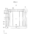
- FIG. 1 shows a top plan view of a photoelectric converting cell module according to an embodiment
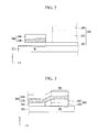
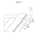
- FIG. 2 shows a cross-sectional view with respect to a line II-II of FIG. 1
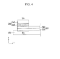
- FIG. 3 shows a cross-sectional view with respect to a line III-III of FIG. 1
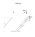
- FIG. 4 shows a cross-sectional view with respect to a line IV-IV of FIG. 1 .
- the photoelectric converting cell module 10 includes a substrate 101, a plurality of photoelectric converting cells 100, interconnect wiring 200, and a bus bar 300.
- the substrate 101 includes an active area (AA) in which a plurality of photoelectric converting cells 100 are formed, and a periphery area (PA) which surrounds the active area (AA) and in which the bus bar 300 is formed.
- the substrate 101 can be formed with various materials including plate-type glass, ceramic, stainless steel, metal, or film-type polymers.
- the photoelectric converting cell 100 is formed in the active area (AA).
- the photoelectric converting cells 100 is extended in a first direction (y-axis direction of FIG. 1 ) of the substrate 101, and is coupled in series in a second direction (x-axis direction of FIG. 1 ) crossing the first direction.
- the photoelectric converting cell 100 includes a rear electrode layer 102, a light absorbing layer (or photoelectric converting layer) 103, and a transparent electrode layer 104 disposed on the substrate 101.
- the rear electrode layer 102 is provided on the substrate 101.
- the rear electrode layer 102 is made of a metal with excellent optical reflective efficiency and excellent adhesion to the substrate 101.
- the rear electrode layer 102 includes molybdenum (Mo).
- Mo molybdenum
- the molybdenum (Mo) has high electrical conductivity, forms an ohmic contact with the photoelectric converting layer 103, and realizes great stability during a high temperature heat treatment for forming the photoelectric converting layer 103.
- the photoelectric converting layer 103 is provided over the rear electrode layer 102.
- the photoelectric converting layer 103 is made of one of silicon and a compound semiconductor.
- the photoelectric converting layer 103 has a semiconductor pn junction or a pin junction structure. Therefore, the photoelectric converting layer 103 includes a p-type semiconductor layer and an n-type semiconductor layer, and an intrinsic semiconductor layer is inserted between the p-type semiconductor layer and the n-type semiconductor layer.
- the photoelectric converting layer 103 is made of a compound semiconductor, it is formed with at least one material of CIGS, CIS, CGS, and CdTe.
- the photoelectric converting layer 103 is formed with at least one material selected from the group of CdTe, CuInSe 2 , Cu(In,Ga)Se 2 , Cu(In,Ga)(Se,S) 2 , Ag(InGa)Se 2 , Cu(In,Al)Se 2 , and CuGaSe 2 .
- the transparent electrode layer 104 is provided over the photoelectric converting layer 103.
- the transparent electrode layer 104 is formed with a metal oxide including boron doped zinc oxide (BZO), zinc oxide (ZnO), indium oxide (In 2 O 3 ), and indium tin oxide (ITO) with excellent light transmittance.
- BZO boron doped zinc oxide
- ZnO zinc oxide
- ITO indium tin oxide
- the transparent electrode layer 104 has great electrical conductivity and great light transmittance.
- the current generated by the photoelectric converting cell 100 is collected by the interconnect wiring 200.
- the interconnect wiring 200 is electrically connected to the photoelectric converting cell 100 formed in the outermost region of the active area (AA).
- a wiring connector (W) formed by partially exposing the rear electrode layer 102 is formed on the photoelectric converting cell 100 formed in the outermost region.
- the interconnect wiring 200 includes a wiring metal layer 240 for collecting the current, and a conductive adhesive layer 220 for adhering the wiring metal layer 240 to the wiring connector (W) of the rear electrode layer 102 and turning them on. That is, the interconnect wiring 200 is a conductive metal tape including the conductive adhesive layer 220. Depending on the cases, the interconnect wiring 200 further includes a black cover layer (not shown) made of a black polyethylene terephthalate (PET) film on the wiring metal layer 240 for the purpose of improving the outer appearance.
- PET polyethylene terephthalate
- the wiring metal layer 240 is a metal foil or a metal ribbon made of copper (Cu), copper (Cu)/tin (Sn), aluminum (Al), lead (Pb), silver (Ag), or an alloy thereof.
- a thickness of the wiring metal layer 240 is between 30 to 400 ⁇ m.
- the wiring metal layer 240 is thicker than 30 ⁇ m in order to secure electric conductivity, and a thicker wiring metal layer 240 is preferred so as to prevent power loss, although the thickness of the wiring metal layer 240 is 400 ⁇ m or less. When the wiring metal layer 240 is thicker than 400 ⁇ m, only the costs are increased without any further improvement to power loss.
- the conductive adhesive layer 220 includes conductive particles, and an adhesive in which the conductive particle are spread.
- the conductive particles are metal particles including at least one of copper (Cu), silver (Ag), gold (Au), iron (Fe), nickel (Ni), lead (Pb), zinc (Zn), cobalt (Co), titanium (Ti), and magnesium (Mg), or plating particles caused by them.
- the conductive particles have a diameter of 10nm-100000nm regarding acquisition of conductivity and maintenance of adhesiveness. When the diameter of a conductive particle is less than 10nm, it is difficult to acquire sufficient conductivity, but when the diameter of the conductive particle is larger than 100000nm, the adhesiveness of the conductive adhesive layer 220 is weak.
- the adhesive in which the conductive particles are spread is an adhesive layer made of a resin including an acryl-based resin, an epoxy-based resin, a butyl-based resin, ethylvinyl acetate (EVA), polyvinyl butyral (PVB), silicon (Si), ionomer, or polyoxy ethylene (POE).
- a resin including an acryl-based resin, an epoxy-based resin, a butyl-based resin, ethylvinyl acetate (EVA), polyvinyl butyral (PVB), silicon (Si), ionomer, or polyoxy ethylene (POE).
- a thickness of the conductive adhesive layer 220 is set considering adhesiveness between the rear electrode layer 102 and the wiring metal layer 240, and contact resistance.
- the thickness of the conductive adhesive layer 220 is from 1 ⁇ m to 500 ⁇ m.
- the conductive adhesive layer 220 is thinner than 1 ⁇ m, the adhesiveness between the rear electrode layer 102 and the wiring metal layer 240 is weak.
- the conductive adhesive layer 220 is thicker than 500 ⁇ m, the contact resistance between the rear electrode layer 102 and the wiring metal layer 240 is increased.
- the interconnect wiring 200 is adhered to the wiring connector (W) by the conductive adhesive layer 220. That is, the interconnect wiring 200 is adhered to a top of the rear electrode layer 102 exposed in the first direction (y-axis direction of FIG. 1 ) of the photoelectric converting cell 100 formed in the outermost region of the active area (AA).
- the current generated by the photoelectric converting cell 100 is collected through the rear electrode layer 102, the conductive adhesive layer 220, and the interconnect wiring 200.
- the interconnect wiring 200 is configured with the wiring metal layer 240 and the conductive adhesive layer 220 for adhering it, the module wiring for collecting the current is easily formed by adhering the metal tape type of interconnect wiring 200 to the wiring connector (W) without a conventional soldering or welding process.
- the interconnect wiring 200 includes an extended portion 201 further extended in the first direction (y-axis direction of FIG. 1 ) of the photoelectric converting cell 100 to reach the periphery area (PA).
- the extended portion 201 is electrically connected to the bus bar 300 formed in the periphery area (PA). According to this, the current collected to the interconnect wiring 200 is transmitted to the bus bar 300, and it is then transmitted to a junction box (not shown) formed outside the photoelectric converting cell module 10 through the bus bar 300.
- the bus bar 300 includes a bus bar metal layer 340 and an insulating adhesive layer 320 for adhering the bus bar metal layer 340 to the substrate 101. That is, the bus bar 300 is an insulating metal tape including the insulating adhesive layer 320.
- the bus bar metal layer 340 is a metal foil or a metal ribbon made of copper (Cu), copper (Cu)/tin (Sn), aluminum (Al), lead (Pb), silver (Ag), or an alloy thereof.
- the insulating adhesive layer 320 is an adhesive layer made of resin including an acryl-based resin, an epoxy-based resin, a butyl-based resin, ethylvinyl acetate (EVA), polyvinyl butyral (PVB), silicon (Si), an ionomer, and polyoxy ethylene (POE).
- the thickness of the insulating adhesive layer 320 is appropriately selected by considering prevention of generation of a leakage current and a step caused by coupling with other components.
- the insulating adhesive layer 320 is substantially thicker than 1 ⁇ m so as to sufficiently insulate a space between the bus bar metal layer 340 and the substrate 101 and prevent a current leakage. Also, it is thinner than 500 ⁇ m in consideration of the interconnect wiring 200 and a sealing member (not shown).
- the bus bar metal layer 340 is adhered to the periphery area (PA) of the substrate 101 by the insulating adhesive layer 320. Therefore, when the current flows to the bus bar metal layer 340, the leakage of current to the substrate 101 is prevented.
- the bus bar 300 includes an overlapped portion 301 overlapped on the extended portion 201 of the interconnect wiring 200 and formed on a first end of the bus bar 300. That is, the conductive adhesive portion 220 of the extended portion 201 is adhered to the bus bar metal layer 340 of the overlapped portion 301. Accordingly, the current collected to the interconnect wiring 200 is transmitted to the bus bar metal layer 340 through the conductive adhesive portion 220 and is then transmitted to an external junction box (not shown) through the bus bar 300.
- bus bar 300 As described, by configuring the bus bar 300 with the bus bar metal layer 340 and the insulating adhesive layer 320 for adhering it on the substrate 101, a bus bar 300 that generates no leakage of current can be formed without an additional insulation process.
- the adhesive layer of the interconnect wiring 200 by configuring the adhesive layer of the interconnect wiring 200 with the conductive adhesive layer 220 and the adhesive layer of the bus bar 300 with the insulating adhesive layer 320, conductivity of the interconnect wiring 200 is acquired (i.e., resistance is reduced) and the generation of leakage current by the bus bar 300 is prevented.
- the insulating adhesive layer 320, the bus bar metal layer 340, the conductive adhesive layer 220, and the wiring metal layer 240 are sequentially stacked on a region in which the extended portion 201 of the interconnect wiring 200 is overlapped with the overlapped portion 301 of the bus bar 300. Accordingly, the interconnect wiring 200 and the bus bar 300 are electrically connected to each other, and the bus bar 300 is sufficiently insulated from the substrate 101. That is, the bus bar 300 can be formed by a simple process, and insulated from the substrate 101 without further processing at the same time, so as to prevent generation of the leakage current, since the bus bar 300 is attached to the substrate 101 by the insulating adhesive layer 320.
- the interconnect wiring 200 can be formed by a simple process, and electrically connected to the rear electrode layer 102 and the bus bar 300 without further processing at the same time, since the interconnect wiring 200 is attached to the rear electrode layer 102 and the bus bar 300 by the conductive adhesive layer 220.
- both of the interconnect wiring 200 and the bus bar 300 are formed by a conductive metal tape, so as to form the module wirings by a simple process without a soldering or welding process. In this case, however, the leakage current is generated from the bus bar 300.
- extra insulating tape must be formed between the bus bar 300 and the substrate 101, so that the additional process attaches the extra insulating tape which increases the entire thickness.
- the interconnect wiring 200 and the bus bar 300 can be formed by a simple process, and at the same time, the generation of the leakage current can be prevented without any extra insulating tape.
- each of the thickness of the adhesive layers 220 and 320 can be appropriately adjusted without increasing the entire thickness of the region overlapping the extended portion 201 and the overlapped portion 301.
- the insulating adhesive layer 320 is thick (e.g., thicker than about 300 ⁇ m), thereby providing sufficient insulation between the substrate 101 and the bus bar metal layer 340
- the conductive adhesive layer 220 can be thinner (e.g., thinner than about 100 ⁇ m) to compensate the increasing thickness of the insulating adhesive layer 320.
- the bus bar metal layer 340 is sufficiently insulated from the substrate 101, so that the generation of the leakage current can be prevented without increasing the entire thickness of the region overlapping the interconnect wiring 200 and the bus bar 300.
- the contact resistance of the interconnect wiring 200 can be decreased by decreasing the transfer distance of electrons through the conductive adhesive layer 220, since the thickness of the conductive adhesive layer 220 is decreased.
- the interconnect wiring 200 is adhered by the conductive adhesive layer 220 including the conductive particles, so relatively uniform contact resistance is maintained without much influence by external moisture and heat.
- FIG. 5 shows a graph for a damp heat test result for a photoelectric converting cell module 10 according to an embodiment.
- the photoelectric converting cell module 10 is left alone for about 1000 hours at a 85 °C temperature in an 85 % moisture condition, and a charge of the contact resistance is measured.
- #1, #2, and #3 show results acquired by performing the same test and measuring it three times.
- the change of the contact resistance is about 2 m ⁇ /cm 2 after the damp heat test given for 1000 hours so the change is not much.
- the contact resistance is increased up to 80 m ⁇ /cm 2 from the contact resistance of 15 m ⁇ /cm 2 after 1000 hours. That is, according to the present embodiment, the conductive adhesive layer 220 has a structure for protecting the conductive particles by the adhesive layer so it can have excellent reliability against external heat and moisture.
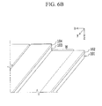
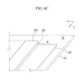
- FIG. 6A to 6F show a method for manufacturing a photoelectric converting cell module according to an embodiment, magnifying a part V of FIG. 1
- FIG. 7 is a flow chart illustrating the process of a method for fabricating a photoelectric converting cell module according to an embodiment.
- a rear electrode layer 102, a photoelectric converting layer 103, and a transparent electrode layer 104 are sequentially stacked on the substrate 101 and patterned to form a plurality of photoelectric converting cells 100 (S100).
- the photoelectric converting layer 103 and the transparent electrode layer 104 of the photoelectric converting cell 100 formed in the outermost region are selectively etched to expose the rear electrode layer 102 (S102).
- the exposed rear electrode layer 102 includes a wiring connector (W) to which the interconnect wiring 200 is adhered.
- the selecting etching process is performed by at least one of the laser scribing method mechanical deletion, wet etching, or paste etching.
- the edges of the rear electrode layer 102, the photoelectric converting layer 103, and the transparent electrode layer 104 are deleted along an edge of the substrate 101 to expose the substrate 101 (S104).
- the deleted portions correspond to the periphery area (PA).
- the deletion process is performed by at least one of the laser scribing method mechanical deletion, wet etching, or paste etching.
- a bus bar 300 is formed in the periphery area (PA) of the substrate 101 (S106).
- the bus bar 300 is formed in a direction (x-axis direction of FIG. 6D ) that is perpendicular to the length direction of the photoelectric converting cell 100.
- the bus bar metal layer 340 is adhered to the substrate 101 by using the insulating adhesive layer 320.
- An opposite first end of the bus bar 300 not shown in FIG. 6D can be electrically connected to a junction box (not shown) disposed outside the photoelectric converting cell module 10.
- an interconnect wiring 200 is formed over the wiring connector (W) of the rear electrode layer 102 and the top of the bus bar 300 (S108).
- the interconnect wiring 200 is formed in a direction (y-axis direction of FIG. 6E ) that is parallel with the length direction of the photoelectric converting cell 100.
- the conductive adhesive layer 220 is used to adhere the wiring metal layer 240 to the wiring connector (W) of the rear electrode layer 102. Also, a part that is passed through the wiring connector (W) and is further extended is adhered to the bus bar metal layer 340 of the bus bar 300.
- the wiring metal layer 240 is electrically connected to the rear electrode layer 102 and the bus bar 300 through the conductive particles in the conductive adhesive layer 220.
- a pressure process is performed regarding the interconnect wiring 200 so as to secure a sufficient electrical connection. That is, the rear electrode 102 (or bus bar metal layer 340), the conductive particle, and the wiring metal layer 240 is contacted and electrically connected to each other by the pressure process.
- the pressure process is separately performed when the interconnect wiring 200 is attached, or is performed with a lamination process (described later) or by pressure of the lamination process.
- a black cover layer (not shown) made of a black polyethylene terephthalate (PET) film is further adhered to the wiring metal layer 240 and the bus bar metal layer 340 so as to improve the appearance. That is, the interconnect wiring 200 with black cover layer thereon is attached to the rear electrode layer 102 and the bus bar 300, and then a tape type black cover layer is attached on the bus bar 300 and the extended portion 201 of the interconnect wiring 200, so that the black cover layer can be formed easily.
- PET polyethylene terephthalate
- a cover substrate (not shown) is disposed on the photoelectric converting cell module 10, and then a sealing process and a lamination process is performed (S 110).
- a frame and a junction box (not shown) are assembled with the photoelectric converting cell module 10 to complete the photoelectric converting cell module 10 (S112).
- the interconnect wiring 200 and the bus bar 300 of the photoelectric converting cell module 10 is formed by adhering the metal tape so the cost is reduced and the process is simplified.
- the adhesive layer of the interconnect wiring 200 is formed with the conductive adhesive layer 240 and the adhesive layer of the bus bar 300 is formed with the insulating adhesive layer 340, thereby acquiring an excellent characteristic through the simple process. That is, interconnect wiring 200 can have excellent current flow without increasing contact resistance regarding the rear electrode layer 102 and the bus bar 300. In addition, generation of the leakage current by the bus bar 300 is prevented since the bus bar 300 is sufficiently insulated from the substrate 101.
Abstract
Description
- The described technology relates generally to a photoelectric converting cell module and a manufacturing method thereof.
- A solar cell is a photovoltaic conversion device for converting light energy of the sun into electrical energy by using the photovoltaic effect. In general, a solar cell module (or photoelectric converting cell module) used for a sunlight electric generator system is an electric device that includes a plurality of photoelectric converting cells coupled in series. A current generated by the electrically connected photoelectric converting cells is collected by the module wiring formed on the solar cell module and is then transmitted to a junction box. The above information disclosed in this Background section is only for enhancement of understanding of the background of the described technology and therefore it may contain information that does not form the prior art that is already known in this country to a person of ordinary skill in the art.
- The described technology has been made in an effort to provide a photoelectric converting cell module for preventing current leakage, providing excellent durability, and allowing an excellent effect with a low cost through a simple and easy process, and a manufacturing method thereof.
- According to the method for manufacturing the photoelectric converting cell module of the present embodiment, the photoelectric converting cell module for generating an excellent effect with a low cost by using a simple and easy process can be manufactured.
- Further, according to the present embodiment, a photoelectric converting cell module without current leakage and with excellent durability is acquired.
- According to an aspect of the present invention, there is provided a photoelectric converting cell module according to
Claim 1. Preferred features of this aspect are set out inClaims 2 to 10. According to a further aspect of the present invention, there is provided a method of manufacturing a photoelectric converting cell module of the current invention according to Claim 11. Preferred embodiments of this aspect are set out in Claims 12 to 15. -
-
FIG. 1 shows a top plan view of a photoelectric converting cell module according to an embodiment. -
FIG. 2 shows a cross-sectional view with respect to a line II-II ofFIG. 1 . -
FIG. 3 shows a cross-sectional view with respect to a line III-IIT ofFIG. 1 . -
FIG. 4 shows a cross-sectional view with respect to a line IV-IV ofFIG. 1 . -
FIG. 5 shows a graph for a damp heat test result according to an embodiment. -
FIG. 6A to 6F show a method for manufacturing a solar cell module according to an embodiment, magnifying a part VI ofFIG. 1 . -
FIG. 7 is a flow chart illustrating the process of a method for fabricating a photoelectric converting cell module according to an embodiment. - The present invention will be described more fully hereinafter with reference to the accompanying drawings, in which embodiments of the invention are shown. As those skilled in the art would realize, the described embodiments may be modified in various different ways, all without departing from the scope of the presently claimed invention.
-
FIG. 1 shows a top plan view of a photoelectric converting cell module according to an embodiment,FIG. 2 shows a cross-sectional view with respect to a line II-II ofFIG. 1 ,FIG. 3 shows a cross-sectional view with respect to a line III-III ofFIG. 1 , andFIG. 4 shows a cross-sectional view with respect to a line IV-IV ofFIG. 1 . - Referring to
FIG. 1 to FIG. 3 , the photoelectricconverting cell module 10 includes asubstrate 101, a plurality ofphotoelectric converting cells 100, interconnectwiring 200, and abus bar 300. - The
substrate 101 includes an active area (AA) in which a plurality of photoelectric convertingcells 100 are formed, and a periphery area (PA) which surrounds the active area (AA) and in which thebus bar 300 is formed. Thesubstrate 101 can be formed with various materials including plate-type glass, ceramic, stainless steel, metal, or film-type polymers. - The
photoelectric converting cell 100 is formed in the active area (AA). Thephotoelectric converting cells 100 is extended in a first direction (y-axis direction ofFIG. 1 ) of thesubstrate 101, and is coupled in series in a second direction (x-axis direction ofFIG. 1 ) crossing the first direction. Thephotoelectric converting cell 100 includes arear electrode layer 102, a light absorbing layer (or photoelectric converting layer) 103, and atransparent electrode layer 104 disposed on thesubstrate 101. - The
rear electrode layer 102 is provided on thesubstrate 101. Therear electrode layer 102 is made of a metal with excellent optical reflective efficiency and excellent adhesion to thesubstrate 101. For example, therear electrode layer 102 includes molybdenum (Mo). The molybdenum (Mo) has high electrical conductivity, forms an ohmic contact with thephotoelectric converting layer 103, and realizes great stability during a high temperature heat treatment for forming thephotoelectric converting layer 103. - The
photoelectric converting layer 103 is provided over therear electrode layer 102. Thephotoelectric converting layer 103 is made of one of silicon and a compound semiconductor. For example, thephotoelectric converting layer 103 has a semiconductor pn junction or a pin junction structure. Therefore, thephotoelectric converting layer 103 includes a p-type semiconductor layer and an n-type semiconductor layer, and an intrinsic semiconductor layer is inserted between the p-type semiconductor layer and the n-type semiconductor layer. Also, when thephotoelectric converting layer 103 is made of a compound semiconductor, it is formed with at least one material of CIGS, CIS, CGS, and CdTe. For example, thephotoelectric converting layer 103 is formed with at least one material selected from the group of CdTe, CuInSe2, Cu(In,Ga)Se2, Cu(In,Ga)(Se,S)2, Ag(InGa)Se2, Cu(In,Al)Se2, and CuGaSe2. - The
transparent electrode layer 104 is provided over thephotoelectric converting layer 103. Thetransparent electrode layer 104 is formed with a metal oxide including boron doped zinc oxide (BZO), zinc oxide (ZnO), indium oxide (In2O3), and indium tin oxide (ITO) with excellent light transmittance. Thetransparent electrode layer 104 has great electrical conductivity and great light transmittance. - The current generated by the
photoelectric converting cell 100 is collected by theinterconnect wiring 200. Theinterconnect wiring 200 is electrically connected to the photoelectric convertingcell 100 formed in the outermost region of the active area (AA). Referring toFIG. 2 , for a connection to theinterconnect wiring 200, a wiring connector (W) formed by partially exposing therear electrode layer 102 is formed on the photoelectric convertingcell 100 formed in the outermost region. - The
interconnect wiring 200 includes awiring metal layer 240 for collecting the current, and a conductiveadhesive layer 220 for adhering thewiring metal layer 240 to the wiring connector (W) of therear electrode layer 102 and turning them on. That is, theinterconnect wiring 200 is a conductive metal tape including the conductiveadhesive layer 220. Depending on the cases, theinterconnect wiring 200 further includes a black cover layer (not shown) made of a black polyethylene terephthalate (PET) film on thewiring metal layer 240 for the purpose of improving the outer appearance. - The
wiring metal layer 240 is a metal foil or a metal ribbon made of copper (Cu), copper (Cu)/tin (Sn), aluminum (Al), lead (Pb), silver (Ag), or an alloy thereof. A thickness of thewiring metal layer 240 is between 30 to 400µm. Thewiring metal layer 240 is thicker than 30µm in order to secure electric conductivity, and a thickerwiring metal layer 240 is preferred so as to prevent power loss, although the thickness of thewiring metal layer 240 is 400µm or less. When thewiring metal layer 240 is thicker than 400µm, only the costs are increased without any further improvement to power loss. - The conductive
adhesive layer 220 includes conductive particles, and an adhesive in which the conductive particle are spread. The conductive particles are metal particles including at least one of copper (Cu), silver (Ag), gold (Au), iron (Fe), nickel (Ni), lead (Pb), zinc (Zn), cobalt (Co), titanium (Ti), and magnesium (Mg), or plating particles caused by them. The conductive particles have a diameter of 10nm-100000nm regarding acquisition of conductivity and maintenance of adhesiveness. When the diameter of a conductive particle is less than 10nm, it is difficult to acquire sufficient conductivity, but when the diameter of the conductive particle is larger than 100000nm, the adhesiveness of the conductiveadhesive layer 220 is weak. The adhesive in which the conductive particles are spread is an adhesive layer made of a resin including an acryl-based resin, an epoxy-based resin, a butyl-based resin, ethylvinyl acetate (EVA), polyvinyl butyral (PVB), silicon (Si), ionomer, or polyoxy ethylene (POE). - A thickness of the conductive
adhesive layer 220 is set considering adhesiveness between therear electrode layer 102 and thewiring metal layer 240, and contact resistance. For example, the thickness of the conductiveadhesive layer 220 is from 1µm to 500µm. When the conductiveadhesive layer 220 is thinner than 1µm, the adhesiveness between therear electrode layer 102 and thewiring metal layer 240 is weak. However, when the conductiveadhesive layer 220 is thicker than 500µm, the contact resistance between therear electrode layer 102 and thewiring metal layer 240 is increased. - The
interconnect wiring 200 is adhered to the wiring connector (W) by the conductiveadhesive layer 220. That is, theinterconnect wiring 200 is adhered to a top of therear electrode layer 102 exposed in the first direction (y-axis direction ofFIG. 1 ) of the photoelectric convertingcell 100 formed in the outermost region of the active area (AA). The current generated by the photoelectric convertingcell 100 is collected through therear electrode layer 102, the conductiveadhesive layer 220, and theinterconnect wiring 200. When theinterconnect wiring 200 is configured with thewiring metal layer 240 and the conductiveadhesive layer 220 for adhering it, the module wiring for collecting the current is easily formed by adhering the metal tape type ofinterconnect wiring 200 to the wiring connector (W) without a conventional soldering or welding process. - Referring to
FIG. 1 andFIG. 3 , theinterconnect wiring 200 includes anextended portion 201 further extended in the first direction (y-axis direction ofFIG. 1 ) of the photoelectric convertingcell 100 to reach the periphery area (PA). Theextended portion 201 is electrically connected to thebus bar 300 formed in the periphery area (PA). According to this, the current collected to theinterconnect wiring 200 is transmitted to thebus bar 300, and it is then transmitted to a junction box (not shown) formed outside the photoelectric convertingcell module 10 through thebus bar 300. - The
bus bar 300 includes a busbar metal layer 340 and an insulatingadhesive layer 320 for adhering the busbar metal layer 340 to thesubstrate 101. That is, thebus bar 300 is an insulating metal tape including the insulatingadhesive layer 320. - The bus
bar metal layer 340 is a metal foil or a metal ribbon made of copper (Cu), copper (Cu)/tin (Sn), aluminum (Al), lead (Pb), silver (Ag), or an alloy thereof. The insulatingadhesive layer 320 is an adhesive layer made of resin including an acryl-based resin, an epoxy-based resin, a butyl-based resin, ethylvinyl acetate (EVA), polyvinyl butyral (PVB), silicon (Si), an ionomer, and polyoxy ethylene (POE). The thickness of the insulatingadhesive layer 320 is appropriately selected by considering prevention of generation of a leakage current and a step caused by coupling with other components. That is, the insulatingadhesive layer 320 is substantially thicker than 1µm so as to sufficiently insulate a space between the busbar metal layer 340 and thesubstrate 101 and prevent a current leakage. Also, it is thinner than 500µm in consideration of theinterconnect wiring 200 and a sealing member (not shown). - The bus
bar metal layer 340 is adhered to the periphery area (PA) of thesubstrate 101 by the insulatingadhesive layer 320. Therefore, when the current flows to the busbar metal layer 340, the leakage of current to thesubstrate 101 is prevented. Thebus bar 300 includes an overlappedportion 301 overlapped on theextended portion 201 of theinterconnect wiring 200 and formed on a first end of thebus bar 300. That is, the conductiveadhesive portion 220 of theextended portion 201 is adhered to the busbar metal layer 340 of the overlappedportion 301. Accordingly, the current collected to theinterconnect wiring 200 is transmitted to the busbar metal layer 340 through the conductiveadhesive portion 220 and is then transmitted to an external junction box (not shown) through thebus bar 300. - As described, by configuring the
bus bar 300 with the busbar metal layer 340 and the insulatingadhesive layer 320 for adhering it on thesubstrate 101, abus bar 300 that generates no leakage of current can be formed without an additional insulation process. - Also, according to the present embodiment, by configuring the adhesive layer of the
interconnect wiring 200 with the conductiveadhesive layer 220 and the adhesive layer of thebus bar 300 with the insulatingadhesive layer 320, conductivity of theinterconnect wiring 200 is acquired (i.e., resistance is reduced) and the generation of leakage current by thebus bar 300 is prevented. - Referring to
FIG. 4 , the insulatingadhesive layer 320, the busbar metal layer 340, the conductiveadhesive layer 220, and thewiring metal layer 240 are sequentially stacked on a region in which theextended portion 201 of theinterconnect wiring 200 is overlapped with the overlappedportion 301 of thebus bar 300. Accordingly, theinterconnect wiring 200 and thebus bar 300 are electrically connected to each other, and thebus bar 300 is sufficiently insulated from thesubstrate 101. That is, thebus bar 300 can be formed by a simple process, and insulated from thesubstrate 101 without further processing at the same time, so as to prevent generation of the leakage current, since thebus bar 300 is attached to thesubstrate 101 by the insulatingadhesive layer 320. Further, theinterconnect wiring 200 can be formed by a simple process, and electrically connected to therear electrode layer 102 and thebus bar 300 without further processing at the same time, since theinterconnect wiring 200 is attached to therear electrode layer 102 and thebus bar 300 by the conductiveadhesive layer 220. - Conventionally, both of the
interconnect wiring 200 and thebus bar 300 are formed by a conductive metal tape, so as to form the module wirings by a simple process without a soldering or welding process. In this case, however, the leakage current is generated from thebus bar 300. Thus, in order to solve this problem, extra insulating tape must be formed between thebus bar 300 and thesubstrate 101, so that the additional process attaches the extra insulating tape which increases the entire thickness. On the other hand, according to the present embodiment, as described above, theinterconnect wiring 200 and thebus bar 300 can be formed by a simple process, and at the same time, the generation of the leakage current can be prevented without any extra insulating tape. - Also, according to the present embodiment, if needed, each of the thickness of the
adhesive layers extended portion 201 and the overlappedportion 301. For example, when the insulatingadhesive layer 320 is thick (e.g., thicker than about 300µm), thereby providing sufficient insulation between thesubstrate 101 and the busbar metal layer 340, the conductiveadhesive layer 220 can be thinner (e.g., thinner than about 100µm) to compensate the increasing thickness of the insulatingadhesive layer 320. In this case, the busbar metal layer 340 is sufficiently insulated from thesubstrate 101, so that the generation of the leakage current can be prevented without increasing the entire thickness of the region overlapping theinterconnect wiring 200 and thebus bar 300. Also, the contact resistance of theinterconnect wiring 200 can be decreased by decreasing the transfer distance of electrons through the conductiveadhesive layer 220, since the thickness of the conductiveadhesive layer 220 is decreased. - Further, the
interconnect wiring 200 is adhered by the conductiveadhesive layer 220 including the conductive particles, so relatively uniform contact resistance is maintained without much influence by external moisture and heat. -
FIG. 5 shows a graph for a damp heat test result for a photoelectric convertingcell module 10 according to an embodiment. The photoelectric convertingcell module 10 is left alone for about 1000 hours at a 85 °C temperature in an 85 % moisture condition, and a charge of the contact resistance is measured. InFIG. 5 , #1, #2, and #3 show results acquired by performing the same test and measuring it three times. As shown inFIG. 5 , regarding the photoelectric convertingcell module 10 according to the present embodiment, it is found that the change of the contact resistance is about 2 mΩ/cm2 after the damp heat test given for 1000 hours so the change is not much. However, when theinterconnect wiring 200 is formed with silver paste in the same condition as the present embodiment, the contact resistance is increased up to 80 mΩ/cm2 from the contact resistance of 15 mΩ/cm2 after 1000 hours. That is, according to the present embodiment, the conductiveadhesive layer 220 has a structure for protecting the conductive particles by the adhesive layer so it can have excellent reliability against external heat and moisture. - A method for manufacturing a photoelectric converting
cell module 10 according to an embodiments will now be described with reference toFIG. 6A to FIG. 6F , andFIG. 7 .FIG. 6A to 6F show a method for manufacturing a photoelectric converting cell module according to an embodiment, magnifying a part V ofFIG. 1 , andFIG. 7 is a flow chart illustrating the process of a method for fabricating a photoelectric converting cell module according to an embodiment. - As shown in
FIG. 6A , arear electrode layer 102, a photoelectric convertinglayer 103, and atransparent electrode layer 104 are sequentially stacked on thesubstrate 101 and patterned to form a plurality of photoelectric converting cells 100 (S100). - As shown in
FIG. 6B , the photoelectric convertinglayer 103 and thetransparent electrode layer 104 of the photoelectric convertingcell 100 formed in the outermost region are selectively etched to expose the rear electrode layer 102 (S102). The exposedrear electrode layer 102 includes a wiring connector (W) to which theinterconnect wiring 200 is adhered. The selecting etching process is performed by at least one of the laser scribing method mechanical deletion, wet etching, or paste etching. - As shown in
FIG. 6C , the edges of therear electrode layer 102, the photoelectric convertinglayer 103, and thetransparent electrode layer 104 are deleted along an edge of thesubstrate 101 to expose the substrate 101 (S104). The deleted portions correspond to the periphery area (PA). The deletion process is performed by at least one of the laser scribing method mechanical deletion, wet etching, or paste etching. - As shown in
FIG. 6D , abus bar 300 is formed in the periphery area (PA) of the substrate 101 (S106). Thebus bar 300 is formed in a direction (x-axis direction ofFIG. 6D ) that is perpendicular to the length direction of the photoelectric convertingcell 100. The busbar metal layer 340 is adhered to thesubstrate 101 by using the insulatingadhesive layer 320. An opposite first end of thebus bar 300 not shown inFIG. 6D can be electrically connected to a junction box (not shown) disposed outside the photoelectric convertingcell module 10. - As shown in
FIG. 6E andFIG. 6F , aninterconnect wiring 200 is formed over the wiring connector (W) of therear electrode layer 102 and the top of the bus bar 300 (S108). Theinterconnect wiring 200 is formed in a direction (y-axis direction ofFIG. 6E ) that is parallel with the length direction of the photoelectric convertingcell 100. The conductiveadhesive layer 220 is used to adhere thewiring metal layer 240 to the wiring connector (W) of therear electrode layer 102. Also, a part that is passed through the wiring connector (W) and is further extended is adhered to the busbar metal layer 340 of thebus bar 300. Therefore, thewiring metal layer 240 is electrically connected to therear electrode layer 102 and thebus bar 300 through the conductive particles in the conductiveadhesive layer 220. At this time, a pressure process is performed regarding theinterconnect wiring 200 so as to secure a sufficient electrical connection. That is, the rear electrode 102 (or bus bar metal layer 340), the conductive particle, and thewiring metal layer 240 is contacted and electrically connected to each other by the pressure process. The pressure process is separately performed when theinterconnect wiring 200 is attached, or is performed with a lamination process (described later) or by pressure of the lamination process. - In addition, if needed, a black cover layer (not shown) made of a black polyethylene terephthalate (PET) film is further adhered to the
wiring metal layer 240 and the busbar metal layer 340 so as to improve the appearance. That is, theinterconnect wiring 200 with black cover layer thereon is attached to therear electrode layer 102 and thebus bar 300, and then a tape type black cover layer is attached on thebus bar 300 and theextended portion 201 of theinterconnect wiring 200, so that the black cover layer can be formed easily. - Thereafter, a cover substrate (not shown) is disposed on the photoelectric converting
cell module 10, and then a sealing process and a lamination process is performed (S 110). A frame and a junction box (not shown) are assembled with the photoelectric convertingcell module 10 to complete the photoelectric converting cell module 10 (S112). - According to the present embodiment, the
interconnect wiring 200 and thebus bar 300 of the photoelectric convertingcell module 10 is formed by adhering the metal tape so the cost is reduced and the process is simplified. - Further, the adhesive layer of the
interconnect wiring 200 is formed with the conductiveadhesive layer 240 and the adhesive layer of thebus bar 300 is formed with the insulatingadhesive layer 340, thereby acquiring an excellent characteristic through the simple process. That is,interconnect wiring 200 can have excellent current flow without increasing contact resistance regarding therear electrode layer 102 and thebus bar 300. In addition, generation of the leakage current by thebus bar 300 is prevented since thebus bar 300 is sufficiently insulated from thesubstrate 101. - While preferred embodiments have been described, it is to be understood that the invention is not limited thereto, but is intended to cover various modifications and equivalent arrangements included within the scope of the appended claims, description, and drawings.
Claims (15)
- A photoelectric converting cell module comprising:a substrate;a plurality of photoelectric converting cells coupled in series;interconnect wiring comprising a wiring metal layer and a conductive adhesive layer; anda bus bar comprising a bus bar metal layer and an insulating adhesive layer, wherein:the substrate includes an active area in which the plurality of photoelectric converting cells are formed, and a periphery area which surrounds the active area and in which the bus bar is formed;the interconnect wiring is electrically coupled to the photoelectric converting cell formed in the outermost region of the active area and extends from the active area to the periphery area and is electrically coupled to the bus bar.
- The photoelectric converting cell module according to Claim 1, wherein each of the plurality of photoelectric converting cells comprises a rear electrode layer, a photoelectric converting layer and a transparent electrode layer disposed in order on top of the substrate.
- The photoelectric converting cell module according to Claim 1 or Claim 2, further comprising a wiring connector that is a partially exposed section of the rear electrode layer of the photoelectric converting cell formed in the outermost region of the active area and forms the electrical connection between the plurality of photoelectric converting cells and the interconnect wiring.
- The photoelectric converting cell module according to Claim 2 or Claim 3, wherein:(a) the photoelectric converting cells extend in a first direction of the substrate and are coupled in series in a second direction perpendicular to the first direction; and/or(b) the substrate is formed from one or more of plate-type glass, ceramic, stainless steel, metal, or film-type polymers; and/or(c) the rear electrode layer is made of a metal or alloy that adheres to the substrate, optionally the metal or alloy comprises molybdenum; and/or(d) the photoelectric converting layer is made of one of silicon and a compound semiconductor; and/or(e) the transparent electrode layer is formed from a metal oxide that comprises one or more of boron doped zinc oxide (BZO), zinc oxide (ZnO), indium oxide (In2O3) and indium tin oxide (ITO); and/or(f) the substrate is formed with plate-type glass, ceramic, stainless steel, metal, or film-type polymers.
- The photoelectric converting cell module according to any one of Claims 1 to 4, wherein:(a) the wiring metal layer is a metal foil or a metal ribbon made of copper (Cu), copper (Cu)/tin (Sn), aluminum (Al), lead (Pb), silver (Ag), or an alloy thereof; and/or(b) the thickness of the wiring metal layer is between 30 to 400µm;
and/or(c) the interconnect wiring is adhered to the wiring connector by the conductive adhesive layer; and/or(d) the interconnect wiring further comprises a black cover layer made of a black polyethylene terephthalate, optionally wherein the interconnect wiring is adhered to a top of the rear electrode layer exposed in the first direction of the photoelectric converting cell formed in the outermost region of the active area. - The photoelectric converting cell module according to any one of Claims 1 to 5, wherein the conductive adhesive layer comprises conductive particles and an adhesive in which the conductive particles are distributed.
- The photoelectric converting cell module according to Claim 6, wherein:(a) the conductive particles are metal particles comprising at least one of copper (Cu), silver (Ag), gold (Au), iron (Fe), nickel (Ni), lead (Pb), zinc (Zn), cobalt (Co), titanium (Ti) and magnesium (Mg) or plating particles caused by said metals; and/or(b) the conductive particles have a diameter of from 10nm to 100,000nm; and/or(c) the adhesive in which the conductive particles are distributed is an adhesive layer made of a resin including an acryl-based resin, an epoxy-based resin, a butyl-based resin, ethylvinyl acetate (EVA), polyvinyl butyral (PVB), silicon (Si), ionomer, or polyoxy ethylene (POE); and/or(d) the thickness of the conductive adhesive layer is from 1µm to 500µm; and/or(e) the conductive particles are distributed homogeneously throughout the adhesive layer.
- The photoelectric converting cell module according to any one of Claims 1 to 7, wherein:(a) the bus bar metal layer is a metal foil or a metal ribbon made of copper (Cu), copper (Cu)/tin (Sn), aluminum (Al), lead (Pb), silver (Ag), or an alloy thereof; and/or(b) the insulating adhesive layer 320 is an adhesive layer made of resin including an acryl-based resin, an epoxy-based resin, a butyl-based resin, ethylvinyl acetate (EVA), polyvinyl butyral (PVB), silicon (Si), an ionomer, and polyoxy ethylene (POE); and/or(c) the insulating adhesive layer is substantially thicker than 1µm and is thinner than 500µm; and/or(d) the bus bar metal layer is adhered to the periphery area (PA) of the substrate by the insulating adhesive layer; and/or(e) the bus bar is formed in a second direction that is perpendicular to the length direction of the plurality of photoelectric converting cells.
- The photoelectric converting cell module according to any one of Claims 1 to 8, wherein the interconnect wiring further comprises an extended portion and the bus bar further comprises an overlapped portion formed on a first end of the bus bar, such that the extended portion of the interconnect wiring overlaps and is attached to the overlapped portion of the bus bar.
- The photoelectric converting cell module according to Claim 9, wherein the insulating adhesive layer, the bus bar metal layer, the conductive adhesive layer, and the wiring metal layer are sequentially stacked on a region in which the extended portion of the interconnect wiring is overlapped with the overlapped portion of the bus bar.
- A method of manufacturing a photoelectric converting cell module according to any one of Claims 1 to 10, comprising the steps of:(a) forming a plurality of photoelectric converting cells coupled in series on a substrate;(b) selectively etching the plurality of photoelectric converting cells on the substrate to generate a wiring connector;(c) deleting the edges of the plurality of photoelectric converting cells are deleted along at least one edge of the substrate to expose the substrate and generate an active area and a periphery area on said substrate, wherein the periphery area corresponds to the exposed substrate and the active area comprises the plurality of photoelectric converting cells and the wiring connector;(d) forming a bus bar on the periphery area of the substrate; and(e) electrically connecting an interconnect wiring to the wiring connector of the rear electrode layer and to the bus bar.
- A method of manufacturing a photoelectric converting cell module according to Claim 11, wherein:(i) in step (a) a rear electrode layer, a photoelectric converting layer, and a transparent electrode layer are sequentially stacked on a substrate and patterned to form the plurality of photoelectric converting cells coupled in series; and/or(ii) in step (b) the photoelectric converting layer and the transparent electrode layer of the photoelectric converting cell formed in the outermost region are selectively etched to expose the rear electrode layer, at least part of said exposed rear electrode layer forming the wiring connector, optionally wherein the etching process is performed by at least one of the laser scribing method, mechanical deletion, wet etching, or paste etching; and/or(iii) in step (c) the edges of the rear electrode layer, the photoelectric converting layer, and the transparent electrode layer of the plurality of photoelectric converting cells are deleted along at least one edge of the substrate to expose the substrate and generate an active area and a periphery area on said substrate, wherein the periphery area corresponds to the exposed substrate and the active area comprises the plurality of photoelectric converting cells and the wiring connector disposed on the substrate, optionally wherein the deletion process is performed by at least one of the laser scribing method, mechanical deletion, wet etching, or paste etching.
- A method of manufacturing a photoelectric converting cell module according to Claim 11 or 12, wherein in step (d):(i) the bus bar is formed on the periphery area of the substrate in a direction that is perpendicular to the length direction of the plurality of photoelectric converting cells; and/or(ii) the bus bar comprises a bus bar metal layer and an insulating adhesive layer as described in any of Claims 1 to 10, such that the bus bar metal layer is adhered to the substrate by using the insulating adhesive layer.
- A method of manufacturing a photoelectric converting cell module according to any one of Claims 11 to 13, wherein in step (e):(i) the interconnect wiring is formed in a direction that is parallel with the length direction of the plurality of photoelectric converting cells; and/or(ii) the interconnect wiring comprises a wiring metal layer and a conductive adhesive layer as described in any of Claims 1 to 10 and wherein the conductive adhesive layer is used to adhere the wiring metal layer to the wiring connector of the rear electrode layer and an extended portion thereof is adhered to the bus bar metal layer of the bus bar; and/or(iii) after application of the interconnect wiring a pressure process is performed so as to secure an electrical connection.
- The method of any one of Claims 11 to 14, further comprising:(A) a step (f) comprising the addition of a black cover layer made of polyethylene terephthalate (PET) is adhered to the wiring metal layer 240 and the bus bar metal layer; and/or(B) a step (g) comprising disposing a cover substrate on the photoelectric converting cell module, and then a sealing process and a lamination process is performed; and/or(C) a step (h) comprising assembling a frame and a junction box with the photoelectric converting cell module to complete the photoelectric converting cell module.
Applications Claiming Priority (2)
| Application Number | Priority Date | Filing Date | Title |
|---|---|---|---|
| US201261699685P | 2012-09-11 | 2012-09-11 | |
| US13/829,224 US20140069479A1 (en) | 2012-09-11 | 2013-03-14 | Photoelectric Device Module and Manufacturing Method Thereof |
Publications (2)
| Publication Number | Publication Date |
|---|---|
| EP2706580A2 true EP2706580A2 (en) | 2014-03-12 |
| EP2706580A3 EP2706580A3 (en) | 2015-10-21 |
Family
ID=48082926
Family Applications (1)
| Application Number | Title | Priority Date | Filing Date |
|---|---|---|---|
| EP13162381.1A Withdrawn EP2706580A3 (en) | 2012-09-11 | 2013-04-04 | Photoelectric device module and manufacturing method thereof |
Country Status (6)
| Country | Link |
|---|---|
| US (1) | US20140069479A1 (en) |
| EP (1) | EP2706580A3 (en) |
| JP (1) | JP2014057059A (en) |
| KR (1) | KR20140034683A (en) |
| CN (1) | CN103681894A (en) |
| IN (1) | IN2013MU02463A (en) |
Families Citing this family (6)
| Publication number | Priority date | Publication date | Assignee | Title |
|---|---|---|---|---|
| US10483410B2 (en) * | 2015-10-20 | 2019-11-19 | Alta Devices, Inc. | Forming front metal contact on solar cell with enhanced resistance to stress |
| JP2019152772A (en) * | 2018-03-05 | 2019-09-12 | 株式会社Joled | Semiconductor device and display device |
| DE102018116466B3 (en) * | 2018-07-06 | 2019-06-19 | Solibro Hi-Tech Gmbh | Thin-film solar module and method for producing a thin-film solar module |
| KR102624328B1 (en) * | 2018-10-31 | 2024-01-15 | 상라오 신위안 웨동 테크놀러지 디벨롭먼트 컴퍼니, 리미티드 | Solar cell module |
| KR20210070762A (en) * | 2019-12-05 | 2021-06-15 | 주식회사 엘지에너지솔루션 | Battery pack comprising thermal progagation blocking member |
| CN115148833A (en) | 2021-03-30 | 2022-10-04 | 金阳(泉州)新能源科技有限公司 | FPCB/FCCL replaces tin-plated copper solder strip as photovoltaic module bus bar |
Family Cites Families (9)
| Publication number | Priority date | Publication date | Assignee | Title |
|---|---|---|---|---|
| US4443652A (en) * | 1982-11-09 | 1984-04-17 | Energy Conversion Devices, Inc. | Electrically interconnected large area photovoltaic cells and method of producing said cells |
| JP2939075B2 (en) * | 1992-12-24 | 1999-08-25 | キヤノン株式会社 | Solar cell module |
| JP4526223B2 (en) * | 2001-06-29 | 2010-08-18 | シャープ株式会社 | Wiring member, solar cell module and manufacturing method thereof |
| JP2005175160A (en) * | 2003-12-10 | 2005-06-30 | Sanyo Electric Co Ltd | Photovoltaic device |
| US20060231802A1 (en) * | 2005-04-14 | 2006-10-19 | Takuya Konno | Electroconductive thick film composition, electrode, and solar cell formed therefrom |
| US8900970B2 (en) * | 2006-04-28 | 2014-12-02 | Semiconductor Energy Laboratory Co., Ltd. | Method for manufacturing a semiconductor device using a flexible substrate |
| US20080245409A1 (en) * | 2006-12-27 | 2008-10-09 | Emcore Corporation | Inverted Metamorphic Solar Cell Mounted on Flexible Film |
| JP5985983B2 (en) * | 2009-06-30 | 2016-09-06 | エルジー イノテック カンパニー リミテッド | Solar power plant |
| KR101168810B1 (en) * | 2010-10-29 | 2012-07-25 | 엘지이노텍 주식회사 | Solar cell apparatus and method of fabricating the same |
-
2013
- 2013-03-14 US US13/829,224 patent/US20140069479A1/en not_active Abandoned
- 2013-04-04 EP EP13162381.1A patent/EP2706580A3/en not_active Withdrawn
- 2013-07-05 KR KR1020130079280A patent/KR20140034683A/en not_active Application Discontinuation
- 2013-07-24 IN IN2463MU2013 patent/IN2013MU02463A/en unknown
- 2013-09-02 JP JP2013181410A patent/JP2014057059A/en active Pending
- 2013-09-11 CN CN201310412302.5A patent/CN103681894A/en active Pending
Non-Patent Citations (1)
| Title |
|---|
| None |
Also Published As
| Publication number | Publication date |
|---|---|
| US20140069479A1 (en) | 2014-03-13 |
| CN103681894A (en) | 2014-03-26 |
| IN2013MU02463A (en) | 2015-07-31 |
| EP2706580A3 (en) | 2015-10-21 |
| JP2014057059A (en) | 2014-03-27 |
| KR20140034683A (en) | 2014-03-20 |
Similar Documents
| Publication | Publication Date | Title |
|---|---|---|
| JP5410050B2 (en) | Solar cell module | |
| JP6224307B2 (en) | Solar cell module | |
| EP2706580A2 (en) | Photoelectric device module and manufacturing method thereof | |
| EP2761674B1 (en) | Photovoltaic cell interconnect | |
| JP2008135655A (en) | Solar battery module, manufacturing method therefor, and solar battery cell | |
| CN103890970B (en) | Photovoltaic cell interconnects | |
| EP2535950B1 (en) | Solar cell module | |
| JP2008010857A (en) | Solar cell module | |
| JP4489126B2 (en) | Solar cell module | |
| US20120090680A1 (en) | Solar cell module and method for manufacturing solar cell module | |
| WO2011129083A1 (en) | Solar cell module and method for manufacturing same | |
| KR101714780B1 (en) | Solar cell module | |
| JP2002252362A (en) | Solar battery module | |
| US20140202528A1 (en) | Thin film solar cell and method of manufacturing the same | |
| US20140246074A1 (en) | Solar module with ribbon cable, and a method for the manufacture of same | |
| WO2011135856A1 (en) | Solar cell module | |
| JP2006041349A (en) | Photovoltaic element and its manufacturing method | |
| JP2012234936A (en) | Photoelectric conversion module and method for manufacturing the same | |
| KR101798148B1 (en) | Solar cell module | |
| WO2014119441A1 (en) | Photoelectric conversion device | |
| WO2013080549A1 (en) | Solar cell module and method for producing same | |
| JP2015170716A (en) | photoelectric conversion module | |
| JP2014146749A (en) | Photoelectric conversion device |
Legal Events
| Date | Code | Title | Description |
|---|---|---|---|
| PUAI | Public reference made under article 153(3) epc to a published international application that has entered the european phase |
Free format text: ORIGINAL CODE: 0009012 |
|
| AK | Designated contracting states |
Kind code of ref document: A2 Designated state(s): AL AT BE BG CH CY CZ DE DK EE ES FI FR GB GR HR HU IE IS IT LI LT LU LV MC MK MT NL NO PL PT RO RS SE SI SK SM TR |
|
| AX | Request for extension of the european patent |
Extension state: BA ME |
|
| PUAL | Search report despatched |
Free format text: ORIGINAL CODE: 0009013 |
|
| AK | Designated contracting states |
Kind code of ref document: A3 Designated state(s): AL AT BE BG CH CY CZ DE DK EE ES FI FR GB GR HR HU IE IS IT LI LT LU LV MC MK MT NL NO PL PT RO RS SE SI SK SM TR |
|
| AX | Request for extension of the european patent |
Extension state: BA ME |
|
| RIC1 | Information provided on ipc code assigned before grant |
Ipc: H01L 31/05 20140101AFI20150911BHEP |
|
| STAA | Information on the status of an ep patent application or granted ep patent |
Free format text: STATUS: THE APPLICATION IS DEEMED TO BE WITHDRAWN |
|
| 18D | Application deemed to be withdrawn |
Effective date: 20160422 |