EP2704343A1 - Multi-wavelength fast tunable transmission device and optical packet switching node - Google Patents
Multi-wavelength fast tunable transmission device and optical packet switching node Download PDFInfo
- Publication number
- EP2704343A1 EP2704343A1 EP12182896.6A EP12182896A EP2704343A1 EP 2704343 A1 EP2704343 A1 EP 2704343A1 EP 12182896 A EP12182896 A EP 12182896A EP 2704343 A1 EP2704343 A1 EP 2704343A1
- Authority
- EP
- European Patent Office
- Prior art keywords
- optical
- transmission device
- subset
- laser
- laser sources
- Prior art date
- Legal status (The legal status is an assumption and is not a legal conclusion. Google has not performed a legal analysis and makes no representation as to the accuracy of the status listed.)
- Granted
Links
Images
Classifications
-
- H—ELECTRICITY
- H01—ELECTRIC ELEMENTS
- H01S—DEVICES USING THE PROCESS OF LIGHT AMPLIFICATION BY STIMULATED EMISSION OF RADIATION [LASER] TO AMPLIFY OR GENERATE LIGHT; DEVICES USING STIMULATED EMISSION OF ELECTROMAGNETIC RADIATION IN WAVE RANGES OTHER THAN OPTICAL
- H01S5/00—Semiconductor lasers
- H01S5/10—Construction or shape of the optical resonator, e.g. extended or external cavity, coupled cavities, bent-guide, varying width, thickness or composition of the active region
- H01S5/12—Construction or shape of the optical resonator, e.g. extended or external cavity, coupled cavities, bent-guide, varying width, thickness or composition of the active region the resonator having a periodic structure, e.g. in distributed feedback [DFB] lasers
-
- H—ELECTRICITY
- H04—ELECTRIC COMMUNICATION TECHNIQUE
- H04Q—SELECTING
- H04Q11/00—Selecting arrangements for multiplex systems
- H04Q11/0001—Selecting arrangements for multiplex systems using optical switching
- H04Q11/0005—Switch and router aspects
-
- H—ELECTRICITY
- H01—ELECTRIC ELEMENTS
- H01S—DEVICES USING THE PROCESS OF LIGHT AMPLIFICATION BY STIMULATED EMISSION OF RADIATION [LASER] TO AMPLIFY OR GENERATE LIGHT; DEVICES USING STIMULATED EMISSION OF ELECTROMAGNETIC RADIATION IN WAVE RANGES OTHER THAN OPTICAL
- H01S5/00—Semiconductor lasers
- H01S5/40—Arrangement of two or more semiconductor lasers, not provided for in groups H01S5/02 - H01S5/30
- H01S5/4012—Beam combining, e.g. by the use of fibres, gratings, polarisers, prisms
-
- H—ELECTRICITY
- H01—ELECTRIC ELEMENTS
- H01S—DEVICES USING THE PROCESS OF LIGHT AMPLIFICATION BY STIMULATED EMISSION OF RADIATION [LASER] TO AMPLIFY OR GENERATE LIGHT; DEVICES USING STIMULATED EMISSION OF ELECTROMAGNETIC RADIATION IN WAVE RANGES OTHER THAN OPTICAL
- H01S5/00—Semiconductor lasers
- H01S5/40—Arrangement of two or more semiconductor lasers, not provided for in groups H01S5/02 - H01S5/30
- H01S5/4025—Array arrangements, e.g. constituted by discrete laser diodes or laser bar
- H01S5/4087—Array arrangements, e.g. constituted by discrete laser diodes or laser bar emitting more than one wavelength
-
- H—ELECTRICITY
- H04—ELECTRIC COMMUNICATION TECHNIQUE
- H04Q—SELECTING
- H04Q11/00—Selecting arrangements for multiplex systems
- H04Q11/0001—Selecting arrangements for multiplex systems using optical switching
- H04Q11/0005—Switch and router aspects
- H04Q2011/0007—Construction
- H04Q2011/0013—Construction using gating amplifiers
-
- H—ELECTRICITY
- H04—ELECTRIC COMMUNICATION TECHNIQUE
- H04Q—SELECTING
- H04Q11/00—Selecting arrangements for multiplex systems
- H04Q11/0001—Selecting arrangements for multiplex systems using optical switching
- H04Q11/0005—Switch and router aspects
- H04Q2011/0007—Construction
- H04Q2011/0015—Construction using splitting combining
-
- H—ELECTRICITY
- H04—ELECTRIC COMMUNICATION TECHNIQUE
- H04Q—SELECTING
- H04Q11/00—Selecting arrangements for multiplex systems
- H04Q11/0001—Selecting arrangements for multiplex systems using optical switching
- H04Q11/0005—Switch and router aspects
- H04Q2011/0007—Construction
- H04Q2011/0018—Construction using tunable transmitters or receivers
Definitions
- the optical transmission device further comprises an output combiner arranged to guide the optical signals passed by the first and second optical gates to a shared optical output.
- the laser sources are distributed feedback (DFB) laser sources.
- DFB distributed feedback
- the outputs of the two SOAs 3 and 5 are connected to a single optical output 7 by an optical combiner 6.
- the optical combiners 2 4 and 6 refer to non-colored components, i.e. capable of passing all wavelengths within the operating range of the transmitter.
Landscapes
- Physics & Mathematics (AREA)
- Condensed Matter Physics & Semiconductors (AREA)
- General Physics & Mathematics (AREA)
- Electromagnetism (AREA)
- Optics & Photonics (AREA)
- Engineering & Computer Science (AREA)
- Computer Networks & Wireless Communication (AREA)
- Optical Communication System (AREA)
Abstract
a multi-wavelength array chip including a plurality of laser sources (DFB1, ... DFB 12),
each laser source being tunable over a respective fine range of wavelengths of the laser source,
a first optical combiner (2) arranged to guide the optical signals generated by a first subset of the laser sources to a first optical gate (3),
a second optical combiner (4) arranged to guide the optical signals generated by a second subset of the laser sources to a second optical gate (5), and
a transmission controller (8) adapted to perform repeatedly a first tuning and sending sequence and a second tuning and sending sequence in a time-offset manner to send optical packets with the first subset of the laser sources and with the second subset of the laser sources at different instants in time on different wavelength channels located within the total range.
Description
- The invention relates to the technical field of wavelength-tunable optical sources, and in particular fast tunable laser sources suitable for optical communication systems employing a packet granularity.
- Optical packet switching networks employing Wavelength Division Multiplexing (WDM) provide flexibility, high capacity and efficient use of the bandwidth through multiplexing techniques in both time and wavelength. Optical packet switching, especially when paired with coherent reception, is a promising technology to realize very efficient networks, e.g. high capacity switch/routers, and to provide an efficient aggregation mechanism in a ring network. An optical packet add and drop multiplexer (OPADM) for a WDM network makes it possible to perform fundamental functions such as optical packet insertion, optical packet extraction and transparent forwarding of transit traffic on each of a plurality of wavelength channels. The optical transparency of the transit path reduces dramatically the number of transponders required to make such equipment.
- As a conventional Reconfigurable Optical Add Drop Multiplexer, an OPADM typically comprises an optical unit managing the transit traffic in the optical domain, dropping traffic to a drop module and adding traffic from an a2dd module, and an electronic unit that comprises the add and drop modules and interfaces with client devices. Examples of OPADM architectures are described in "Optical Packet Add/Drop Multiplexers for packet ring networks," Proceedings of ECOC 2008, Brussels Expo, Belgium, pp 103-106, XP001524738, in
EP-A1-2160045 andEP-A1-2458761 . - In an embodiment, the invention provides a wavelength-tunable optical transmission device comprising:
- a multi-wavelength array chip including a plurality of laser sources, each laser source being tunable over a respective fine range of wavelengths of the laser source, wherein the fine ranges of the plurality of laser sources continuously span a total range of wavelengths of the laser optical transmission device, characterized by:
- a first optical combiner arranged to guide the optical signals generated by a first subset of the laser sources to a first optical gate,
- a second optical combiner arranged to guide the optical signals generated by a second subset of the laser sources to a second optical gate, and
- a transmission controller adapted to perform repeatedly a first tuning and sending sequence and a second tuning and sending sequence in a time-offset manner to send optical packets with the first subset of the laser sources and with the second subset of the laser sources at different instants in time on different wavelength channels located within the total range,
- wherein the first tuning and sending sequence comprises closing the first optical gate, selecting a laser source in the first subset as a function of a first target wavelength channel so that the fine range of the laser source includes the first target wavelength channel, tuning the selected laser source to the first target wavelength channel and opening the first optical gate, and
- wherein the second tuning and sending sequence comprises closing the second optical gate, selecting a laser source in the second subset as a function of a second target wavelength channel so that the fine range of the laser source includes the second target wavelength channel, tuning the selected laser source to the second target wavelength channel and opening the second optical gate.
- In an embodiment, the optical transmission device further comprises an output combiner arranged to guide the optical signals passed by the first and second optical gates to a shared optical output.
- In an embodiment, the optical transmission device further comprises an optical modulator arranged for modulating the optical signals passed by the optical output.
- In an embodiment, the optical modulator is adapted to modulate the optical signals in accordance with a multilevel Quadrature Amplitude Modulation scheme.
- In an embodiment, the fine range of each laser source spans 2.7 nm or more.
- In an embodiment, the fine tuning of a laser source is performed by controlling a temperature of the laser source.
- In an embodiment, the laser sources are in the number of 12 or more.
- In an embodiment, the laser sources in a subset are in the number of 6 or more.
- In an embodiment, the total range of wavelengths spans 32 nm or more in the C band.
- In an embodiment, the laser sources are distributed feedback (DFB) laser sources.
- In an embodiment, the invention also provides an optical packet switching node comprising:
- an input section for receiving optical packets,
- a controller adapted to receive control data associated to the optical packets,
- an output section for transmitting optical packets,
- an optical transit section adapted to pass optical packets from the input section to the output section, and
- an optical packet drop section including an optical packet receiver connected to the input section and adapted to demodulate an optical packet,
- and an optical packet add section including an optical transmission device adapted to transmit an optical packet to the output section
- Aspects of the invention stem from the observation that fast tunable lasers are required to fully benefit from the advantages of optical packet switching in WDM networks.
- Aspects of the invention stem from the observation that tunable lasers cannot be switched as fast as a few nanoseconds, which would be necessary to tune the wavelength during the time between two packets, and cannot be maintained stable with a narrow linewidth for the packet duration, which would be necessary for optimal operation of a coherent receiver.
- Aspects of the invention are based on the idea of providing a transmitter device capable of tuning the output wavelength in as short a time as tens or hundreds of nanoseconds.
- These and other aspects of the invention will be apparent from and elucidated with reference to the embodiments described hereinafter, by way of example, with reference to the drawings.
-
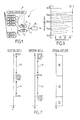
Figure 1 is a functional representation of a tunable optical packet transmitter. -
Figure 2 is a flow diagram showing an operation of the transmitter ofFig.1 in time. -
Figure 3 is a graph showing the range of wavelengths attainable by each of the DFB laser sources of the transmitter ofFig. 1 . - With reference to
Figure 1 , a tunableoptical packet transmitter 1 comprises a plurality of DFB laser sources. The embodiment shown comprises 12 laser sources designated as DFB1 to DFB12. A higher or lower number of DFB laser sources can be made in the same manner. - The DFB laser sources can be made in an integrated manner as a multi-wavelength array chip. Further details about the making of such an array chip are disclosed in B. Pezeshki et al., "12 element multi-wavelength DFB arrays for widely tunable laser modules", paper ThGG71, OFC 2002, pp 711-712. Such an array chip offers the advantages of a simple, compact, low-cost and high-yield chip design with proven technological maturity. The disclosed 12 elements multi-wavelength array can be tuned over 32nm in the C band. Each element of the multi-wavelength array can be individually tuned over 2.7nm through temperature control.
- As shown on
Fig. 1 , the laser sources DFB1 to DFB12 are split in two subsets or more through the use of optical combiners. More precisely, the optical combiner 2 couples the outputs of a first half of the laser sources to a semiconductor optical amplifier (SOA) 3 that operates as an optical gate. Similarly, the optical combiner 4 couples the outputs of a second half of the laser sources to a semiconductor optical amplifier (SOA) 5 that operates as a second optical gate. In the embodiment shown, the first subset comprises all laser sources with an odd rank and the second subset comprises all laser sources with an even rank. However, the grouping could be done otherwise. - The outputs of the two SOAs 3 and 5 are connected to a single optical output 7 by an optical combiner 6. The
optical combiners 2 4 and 6 refer to non-colored components, i.e. capable of passing all wavelengths within the operating range of the transmitter. - The wavelength tunability of the
transmitter 1 is illustrated inFig. 3 . Namely, each DFB source has a unique fine-tuning range shown by a continuous line inFig. 3 . The lowest line corresponds to DFB1 and the top line to DFB12. Together, the fine tuning ranges of the DFB sources span the entire interval 1532 to 1565 nm, with some overlap. The left-hand side vertical axis onFig. 3 shows the spectral intervals that can be attained by the DFB sources in the first subset and the righthand side vertical axis onFig. 3 shows the spectral intervals that can be attained by the DFB sources in the second subset. - With reference to
Figure 2 , the operation of the fast tunable transmitter will now be described.Figure 2 depicts a process that is performed repeatedly in time under the control of acontrol unit 8. In this process, the optical gates 3 and 5 are alternatively opened and closed in opposition so that only one of the two subsets can send an optical signal at every instant in time. While an optical gate remains open, a laser source that has been previously tuned to the desired wavelength sends an optical signal, which reaches the transmitter output 7. During that period depicted byarrow 12, a laser source in the other subset is being tuned to the desired wavelength channel for the next packet to be emitted. Therefore, the time period taken by the tuning process, which is depicted byarrow 11, overlaps entirely or almost entirely the transmittingperiod 12 of the other source. In this manner, it is possible to set the inter-packet interval, i.e. the time gap between two consecutive packets sent by thetransmitter 1 independently form the duration of the tuning process. Furthermore, as shown, the inter-packet interval can be reduced to almost zero to optimize capacity. - The
control unit 8 performs an identical sequence of operations with each of the two subsets of optical sources, namely: - Closing the optical gate at the end of the optical packet being sent,
- obtaining the next wavelength to be transmitted, which could be communicated e.g. as a standard ITU channel number by a node controller,
- selecting a laser source within the subset of which the tuning range contains the next wavelength,
- activating and tuning the laser source by temperature control, and
- opening the optical gate when the optical packet must be sent.
-
Figure 2 also shows the optical signals obtained at the output 7, namely a firstoptical packet 10 sent by a source of the first subset, then a secondoptical packet 20 sent by a source of the second subset, then a thirdoptical packet 30 sent by a source of the first subset, and so on. - This process may take place in a synchronous network, e.g. as disclosed in
EP-A1-2458761 . In particular, thetransmitter 1 can be installed in the add module of a packet switching node. A constraint results from the fact that a subset of the sources may not be able to tune to all wavelengths channels, as shown onFig. 3 . Therefore, a subset may sometimes not be capable of sending useful traffic at its turn, due to a mismatch between the desired wavelength and the tuning range of the subset. Overall, such instances do not substantially degrade the network efficiency thanks to the possibility for other nodes in the packet network to reuse the time slot left available. Furthermore, wavelength assignment can be optimized to reduce the probability of such mismatches. -
Fig. 1 also shows an externaloptical modulator 15 arranged at the output 7 to modulate the sent optical packets. In an embodiment, a modulation scheme with a large constellation such as QAM16 or QAM64 is used. For such constellations, the narrow linewidth of the laser sources is critical. - In the above-described embodiment, the laser sources are distributed feedback (DFB) laser sources. Other sorts of laser sources can be arranged and used in the same manner, e.g. any flavor of distributed Bragg grating (DBR) sources.
- Elements such as the control units could be e.g. hardware means like e.g. an ASIC, or a combination of hardware and software means, e.g. an ASIC and an FPGA, or at least one microprocessor and at least one memory with software modules located therein.
- The invention is not limited to the described embodiments. The appended claims are to be construed as embodying all modification and alternative constructions that may be occurred to one skilled in the art, which fairly fall within the basic teaching here, set forth.
- The use of the verb "to comprise" or "to include" and its conjugations does not exclude the presence of elements or steps other than those stated in a claim. Furthermore, the use of the article "a" or "an" preceding an element or step does not exclude the presence of a plurality of such elements or steps.
- In the claims, any reference signs placed between parentheses shall not be construed as limiting the scope of the claims.
Claims (11)
- A wavelength-tunable optical transmission device (1) comprising:a multi-wavelength array chip including a plurality of (DFB1, ... DFB 12) laser sources,each laser source being tunable over a respective fine range of wavelengths of the laser source, wherein the fine ranges of the plurality of laser sources continuously span a total range of wavelengths of the laser optical transmission device,characterized by:a first optical combiner (2) arranged to guide the optical signals generated by a first subset of the laser sources to a first optical gate (3),a second optical combiner (4) arranged to guide the optical signals generated by a second subset of the laser sources to a second optical gate (5), anda transmission controller (8) adapted to perform repeatedly a first tuning and sending sequence and a second tuning and sending sequence in a time-offset manner to send optical packets (10, 20, 30) with the first subset of the laser sources and with the second subset of the laser sources at different instants in time on different wavelength channels located within the total range,wherein the first tuning and sending sequence comprises closing the first optical gate (3), selecting a laser source in the first subset as a function of a first target wavelength channel so that the fine range of the laser source includes the first target wavelength channel, tuning (11) the selected laser source to the first target wavelength channel and opening the first optical gate (3), andwherein the second tuning and sending sequence comprises closing the second optical gate (5), selecting a laser source in the second subset as a function of a second target wavelength channel so that the fine range of the laser source includes the second target wavelength channel, tuning (11) the selected laser source to the second target wavelength channel and opening the second optical gate (5).
- The optical transmission device in accordance with claim 1, further comprising an output combiner (6) arranged to guide the optical signals passed by the first and second optical gates to a shared optical output (7).
- The optical transmission device in accordance with claim 2, further comprising an optical modulator (15) arranged for modulating the optical signals passed by the optical output (7).
- The optical transmission device in accordance with claim 3, wherein the optical modulator (15) is adapted to modulate the optical signals in accordance with a multilevel Quadrature Amplitude Modulation scheme.
- The optical transmission device in accordance with any one of claims 1 to 4, wherein the fine range of each laser source spans 2.7 nm or more.
- The optical transmission device in accordance with any one of claims 1 to 5, wherein the fine tuning of a laser source is performed by controlling a temperature of the laser source.
- The optical transmission device in accordance any one of claims 1 to 6, wherein the laser sources are in the number of 12 or more.
- The optical transmission device in accordance any one of claims 1 to 7, wherein the laser sources in a subset are in the number of 6 or more.
- The optical transmission device in accordance any one of claims 1 to 8, wherein the total range of wavelengths spans 32 nm or more in the C band.
- The optical transmission device in accordance any one of claims 1 to 9, wherein the laser sources are distributed feedback laser sources.
- An optical packet switching node comprising:an input section for receiving optical packets,a controller adapted to receive control data associated to the optical packets,an output section for transmitting optical packets,an optical transit section adapted to pass optical packets from the input section to the output section, andan optical packet drop section including an optical packet receiver connected to the input section and adapted to demodulate an optical packet,and an optical packet add section including an optical transmission device (1) adapted to transmit an optical packet to the output section, characterized in that the optical transmission device is accordance with any one of claims 1 to 10.
Priority Applications (1)
| Application Number | Priority Date | Filing Date | Title |
|---|---|---|---|
| EP12182896.6A EP2704343B1 (en) | 2012-09-04 | 2012-09-04 | Multi-wavelength fast tunable transmission device and optical packet switching node |
Applications Claiming Priority (1)
| Application Number | Priority Date | Filing Date | Title |
|---|---|---|---|
| EP12182896.6A EP2704343B1 (en) | 2012-09-04 | 2012-09-04 | Multi-wavelength fast tunable transmission device and optical packet switching node |
Publications (2)
| Publication Number | Publication Date |
|---|---|
| EP2704343A1 true EP2704343A1 (en) | 2014-03-05 |
| EP2704343B1 EP2704343B1 (en) | 2015-11-04 |
Family
ID=46796442
Family Applications (1)
| Application Number | Title | Priority Date | Filing Date |
|---|---|---|---|
| EP12182896.6A Active EP2704343B1 (en) | 2012-09-04 | 2012-09-04 | Multi-wavelength fast tunable transmission device and optical packet switching node |
Country Status (1)
| Country | Link |
|---|---|
| EP (1) | EP2704343B1 (en) |
Cited By (3)
| Publication number | Priority date | Publication date | Assignee | Title |
|---|---|---|---|---|
| CN106887790A (en) * | 2017-04-13 | 2017-06-23 | 中国科学院半导体研究所 | Multi-wavelength silicon substrate hybrid integrated slot laser arrays and preparation method thereof |
| CN106921112A (en) * | 2017-04-13 | 2017-07-04 | 中国科学院半导体研究所 | Multi-wavelength silicon substrate hybrid integrated slot laser integrated optical sources and preparation method thereof |
| CN113253539A (en) * | 2021-05-31 | 2021-08-13 | 南京邮电大学 | All-optical packet switch based on integrated SOA series tunable laser |
Families Citing this family (1)
| Publication number | Priority date | Publication date | Assignee | Title |
|---|---|---|---|---|
| CN110995354B (en) * | 2019-12-19 | 2021-05-14 | 成都优博创通信技术股份有限公司 | Optical assembly and optical module |
Citations (2)
| Publication number | Priority date | Publication date | Assignee | Title |
|---|---|---|---|---|
| EP2160045A1 (en) | 2008-08-25 | 2010-03-03 | Alcatel Lucent | Optical packet communication node |
| EP2458761A1 (en) | 2010-11-29 | 2012-05-30 | Alcatel Lucent | Optical packet switching node |
-
2012
- 2012-09-04 EP EP12182896.6A patent/EP2704343B1/en active Active
Patent Citations (2)
| Publication number | Priority date | Publication date | Assignee | Title |
|---|---|---|---|---|
| EP2160045A1 (en) | 2008-08-25 | 2010-03-03 | Alcatel Lucent | Optical packet communication node |
| EP2458761A1 (en) | 2010-11-29 | 2012-05-30 | Alcatel Lucent | Optical packet switching node |
Non-Patent Citations (4)
| Title |
|---|
| "Optical Packet Add/Drop Multiplexers for packet ring networks", PROCEEDINGS OF ECOC 2008, BRUSSELS EXPO, BELGIUM, pages 103 - 106 |
| B. PEZESHKI ET AL.: "12 element multi-wavelength DFB arrays for widely tunable laser modules", OFC, 2002, pages 711 - 712 |
| KOTAKI Y ET AL: "Wavelength tunable DFB laser array for WDM applications", ECOC 2002. 28TH EUROPEAN CONFERENCE ON OPTICAL COMMUNICATION (IEEE CAT. NO. 02TH8640) IEEE PISCATAWAY, NJ, USA, vol. 2, 2002, XP002688049, ISBN: 87-90974-64-6, Retrieved from the Internet <URL:http://ieeexplore.ieee.org/stamp/stamp.jsp?tp=&arnumber=1600970> [retrieved on 20121126] * |
| PEZESHKI B ET AL: "12 element multi-wavelength DFB arrays for widely tunable laser modules", OPTICAL FIBER COMMUNICATIONS CONFERENCE. (OFC). POSTCONFERENCE TECHNICAL DIGEST. POSTDEADLINE PAPERS (IEEE CAT. NO.02CH37339) OPT SOC. AMERICA WASHINGTON, DC, USA; [TRENDS IN OPTICS AND PHOTONICS SERIES. (TOPS)], IEEE, vol. TOPS. VOL. 70, 17 March 2002 (2002-03-17), pages 711 - 712, XP010618084, ISBN: 978-1-55752-701-1, DOI: 10.1109/OFC.2002.1036667 * |
Cited By (3)
| Publication number | Priority date | Publication date | Assignee | Title |
|---|---|---|---|---|
| CN106887790A (en) * | 2017-04-13 | 2017-06-23 | 中国科学院半导体研究所 | Multi-wavelength silicon substrate hybrid integrated slot laser arrays and preparation method thereof |
| CN106921112A (en) * | 2017-04-13 | 2017-07-04 | 中国科学院半导体研究所 | Multi-wavelength silicon substrate hybrid integrated slot laser integrated optical sources and preparation method thereof |
| CN113253539A (en) * | 2021-05-31 | 2021-08-13 | 南京邮电大学 | All-optical packet switch based on integrated SOA series tunable laser |
Also Published As
| Publication number | Publication date |
|---|---|
| EP2704343B1 (en) | 2015-11-04 |
Similar Documents
| Publication | Publication Date | Title |
|---|---|---|
| US6014237A (en) | Multiwavelength mode-locked dense wavelength division multiplexed optical communication systems | |
| US8818207B2 (en) | Optical transmitter | |
| EP2173043B1 (en) | Integrated optical comb source system and method | |
| KR0157429B1 (en) | Transmission apparatus and optical signal system of wavelength division multiplexing optical communication system | |
| US8571419B2 (en) | Method and system for flexible optical signal aggregation and transmission | |
| US20200343680A1 (en) | Wavelength switchable laser | |
| EP2704343B1 (en) | Multi-wavelength fast tunable transmission device and optical packet switching node | |
| US8849128B2 (en) | Multi-wavelength light source | |
| US10396901B2 (en) | Reception of multiple-wavelength optical signals consisting of single-band optical bursts | |
| EP2913943A1 (en) | Optical communication with spatially multiplexed optical packet signals | |
| US10263722B2 (en) | Multi-wavelength balanced optical transmission networks | |
| Proietti et al. | Quasi-hitless defragmentation technique in elastic optical networks by a coherent RX LO with fast TX wavelength tracking | |
| EP1345342A1 (en) | An optical transmitter for transmitting signals with high data rates, an optical transmission system and a method therefor | |
| CN103517161B (en) | The method communicated between local side apparatus and optical network unit in EPON | |
| Zervas et al. | QoS-aware ingress optical grid user network interface: high-speed ingress OBS node design and implementation | |
| Ware et al. | Towards WDM slot switching for aggregation access and metropolitan applications: the ANR N-GREEN project | |
| EP2773057A1 (en) | Optical network node and method of transmitting wavelength multiplexed optical data signals | |
| JPH0591052A (en) | Wavelength switching device and method | |
| US11909512B1 (en) | Methods of injection locking for multiple optical source generation | |
| JP7270852B1 (en) | Optical transmission device and optical transmission method | |
| US7848655B2 (en) | Mode-locked optical amplifier as a source for a wdm-WDM hierarchy architecture | |
| US20250113124A1 (en) | Sub-passband ramping as a method of managing power transients in c+l band optical line networks | |
| WO2009120219A1 (en) | Dynamic signal equalization in optical transmission systems | |
| Betoule et al. | Impact of optical flexibility and sub-band switching on multi-layer transport network architectures | |
| Altabas et al. | Design of flexible udWDM metro-access network devices assisted by high resolution complex spectroscopy |
Legal Events
| Date | Code | Title | Description |
|---|---|---|---|
| AK | Designated contracting states |
Kind code of ref document: A1 Designated state(s): AL AT BE BG CH CY CZ DE DK EE ES FI FR GB GR HR HU IE IS IT LI LT LU LV MC MK MT NL NO PL PT RO RS SE SI SK SM TR |
|
| AX | Request for extension of the european patent |
Extension state: BA ME |
|
| PUAI | Public reference made under article 153(3) epc to a published international application that has entered the european phase |
Free format text: ORIGINAL CODE: 0009012 |
|
| 17P | Request for examination filed |
Effective date: 20140408 |
|
| RBV | Designated contracting states (corrected) |
Designated state(s): AL AT BE BG CH CY CZ DE DK EE ES FI FR GB GR HR HU IE IS IT LI LT LU LV MC MK MT NL NO PL PT RO RS SE SI SK SM TR |
|
| 111Z | Information provided on other rights and legal means of execution |
Free format text: AL AT BE BG CH CY CZ DE DK EE ES FI FR GB GR HR HU IE IS IT LI LT LU LV MC MK MT NL NO PL PT RO RS SE SI SK SM TR Effective date: 20140516 |
|
| RAP1 | Party data changed (applicant data changed or rights of an application transferred) |
Owner name: ALCATEL LUCENT |
|
| D11X | Information provided on other rights and legal means of execution (deleted) | ||
| GRAP | Despatch of communication of intention to grant a patent |
Free format text: ORIGINAL CODE: EPIDOSNIGR1 |
|
| INTG | Intention to grant announced |
Effective date: 20150526 |
|
| GRAS | Grant fee paid |
Free format text: ORIGINAL CODE: EPIDOSNIGR3 |
|
| GRAA | (expected) grant |
Free format text: ORIGINAL CODE: 0009210 |
|
| AK | Designated contracting states |
Kind code of ref document: B1 Designated state(s): AL AT BE BG CH CY CZ DE DK EE ES FI FR GB GR HR HU IE IS IT LI LT LU LV MC MK MT NL NO PL PT RO RS SE SI SK SM TR |
|
| REG | Reference to a national code |
Ref country code: GB Ref legal event code: FG4D |
|
| REG | Reference to a national code |
Ref country code: CH Ref legal event code: EP |
|
| REG | Reference to a national code |
Ref country code: AT Ref legal event code: REF Ref document number: 759820 Country of ref document: AT Kind code of ref document: T Effective date: 20151115 |
|
| REG | Reference to a national code |
Ref country code: IE Ref legal event code: FG4D |
|
| REG | Reference to a national code |
Ref country code: DE Ref legal event code: R096 Ref document number: 602012012101 Country of ref document: DE |
|
| REG | Reference to a national code |
Ref country code: NL Ref legal event code: MP Effective date: 20151104 |
|
| REG | Reference to a national code |
Ref country code: LT Ref legal event code: MG4D |
|
| REG | Reference to a national code |
Ref country code: AT Ref legal event code: MK05 Ref document number: 759820 Country of ref document: AT Kind code of ref document: T Effective date: 20151104 |
|
| PG25 | Lapsed in a contracting state [announced via postgrant information from national office to epo] |
Ref country code: IT Free format text: LAPSE BECAUSE OF FAILURE TO SUBMIT A TRANSLATION OF THE DESCRIPTION OR TO PAY THE FEE WITHIN THE PRESCRIBED TIME-LIMIT Effective date: 20151104 Ref country code: ES Free format text: LAPSE BECAUSE OF FAILURE TO SUBMIT A TRANSLATION OF THE DESCRIPTION OR TO PAY THE FEE WITHIN THE PRESCRIBED TIME-LIMIT Effective date: 20151104 Ref country code: NO Free format text: LAPSE BECAUSE OF FAILURE TO SUBMIT A TRANSLATION OF THE DESCRIPTION OR TO PAY THE FEE WITHIN THE PRESCRIBED TIME-LIMIT Effective date: 20160204 Ref country code: IS Free format text: LAPSE BECAUSE OF FAILURE TO SUBMIT A TRANSLATION OF THE DESCRIPTION OR TO PAY THE FEE WITHIN THE PRESCRIBED TIME-LIMIT Effective date: 20160304 Ref country code: LT Free format text: LAPSE BECAUSE OF FAILURE TO SUBMIT A TRANSLATION OF THE DESCRIPTION OR TO PAY THE FEE WITHIN THE PRESCRIBED TIME-LIMIT Effective date: 20151104 Ref country code: NL Free format text: LAPSE BECAUSE OF FAILURE TO SUBMIT A TRANSLATION OF THE DESCRIPTION OR TO PAY THE FEE WITHIN THE PRESCRIBED TIME-LIMIT Effective date: 20151104 Ref country code: HR Free format text: LAPSE BECAUSE OF FAILURE TO SUBMIT A TRANSLATION OF THE DESCRIPTION OR TO PAY THE FEE WITHIN THE PRESCRIBED TIME-LIMIT Effective date: 20151104 |
|
| PG25 | Lapsed in a contracting state [announced via postgrant information from national office to epo] |
Ref country code: FI Free format text: LAPSE BECAUSE OF FAILURE TO SUBMIT A TRANSLATION OF THE DESCRIPTION OR TO PAY THE FEE WITHIN THE PRESCRIBED TIME-LIMIT Effective date: 20151104 Ref country code: PL Free format text: LAPSE BECAUSE OF FAILURE TO SUBMIT A TRANSLATION OF THE DESCRIPTION OR TO PAY THE FEE WITHIN THE PRESCRIBED TIME-LIMIT Effective date: 20151104 Ref country code: LV Free format text: LAPSE BECAUSE OF FAILURE TO SUBMIT A TRANSLATION OF THE DESCRIPTION OR TO PAY THE FEE WITHIN THE PRESCRIBED TIME-LIMIT Effective date: 20151104 Ref country code: GR Free format text: LAPSE BECAUSE OF FAILURE TO SUBMIT A TRANSLATION OF THE DESCRIPTION OR TO PAY THE FEE WITHIN THE PRESCRIBED TIME-LIMIT Effective date: 20160205 Ref country code: SE Free format text: LAPSE BECAUSE OF FAILURE TO SUBMIT A TRANSLATION OF THE DESCRIPTION OR TO PAY THE FEE WITHIN THE PRESCRIBED TIME-LIMIT Effective date: 20151104 Ref country code: AT Free format text: LAPSE BECAUSE OF FAILURE TO SUBMIT A TRANSLATION OF THE DESCRIPTION OR TO PAY THE FEE WITHIN THE PRESCRIBED TIME-LIMIT Effective date: 20151104 Ref country code: RS Free format text: LAPSE BECAUSE OF FAILURE TO SUBMIT A TRANSLATION OF THE DESCRIPTION OR TO PAY THE FEE WITHIN THE PRESCRIBED TIME-LIMIT Effective date: 20151104 Ref country code: PT Free format text: LAPSE BECAUSE OF FAILURE TO SUBMIT A TRANSLATION OF THE DESCRIPTION OR TO PAY THE FEE WITHIN THE PRESCRIBED TIME-LIMIT Effective date: 20160304 |
|
| PG25 | Lapsed in a contracting state [announced via postgrant information from national office to epo] |
Ref country code: CZ Free format text: LAPSE BECAUSE OF FAILURE TO SUBMIT A TRANSLATION OF THE DESCRIPTION OR TO PAY THE FEE WITHIN THE PRESCRIBED TIME-LIMIT Effective date: 20151104 |
|
| REG | Reference to a national code |
Ref country code: DE Ref legal event code: R097 Ref document number: 602012012101 Country of ref document: DE |
|
| PG25 | Lapsed in a contracting state [announced via postgrant information from national office to epo] |
Ref country code: SM Free format text: LAPSE BECAUSE OF FAILURE TO SUBMIT A TRANSLATION OF THE DESCRIPTION OR TO PAY THE FEE WITHIN THE PRESCRIBED TIME-LIMIT Effective date: 20151104 Ref country code: RO Free format text: LAPSE BECAUSE OF FAILURE TO SUBMIT A TRANSLATION OF THE DESCRIPTION OR TO PAY THE FEE WITHIN THE PRESCRIBED TIME-LIMIT Effective date: 20151104 Ref country code: DK Free format text: LAPSE BECAUSE OF FAILURE TO SUBMIT A TRANSLATION OF THE DESCRIPTION OR TO PAY THE FEE WITHIN THE PRESCRIBED TIME-LIMIT Effective date: 20151104 Ref country code: EE Free format text: LAPSE BECAUSE OF FAILURE TO SUBMIT A TRANSLATION OF THE DESCRIPTION OR TO PAY THE FEE WITHIN THE PRESCRIBED TIME-LIMIT Effective date: 20151104 Ref country code: SK Free format text: LAPSE BECAUSE OF FAILURE TO SUBMIT A TRANSLATION OF THE DESCRIPTION OR TO PAY THE FEE WITHIN THE PRESCRIBED TIME-LIMIT Effective date: 20151104 |
|
| PLBE | No opposition filed within time limit |
Free format text: ORIGINAL CODE: 0009261 |
|
| STAA | Information on the status of an ep patent application or granted ep patent |
Free format text: STATUS: NO OPPOSITION FILED WITHIN TIME LIMIT |
|
| REG | Reference to a national code |
Ref country code: FR Ref legal event code: PLFP Year of fee payment: 5 |
|
| 26N | No opposition filed |
Effective date: 20160805 |
|
| PG25 | Lapsed in a contracting state [announced via postgrant information from national office to epo] |
Ref country code: SI Free format text: LAPSE BECAUSE OF FAILURE TO SUBMIT A TRANSLATION OF THE DESCRIPTION OR TO PAY THE FEE WITHIN THE PRESCRIBED TIME-LIMIT Effective date: 20151104 |
|
| PG25 | Lapsed in a contracting state [announced via postgrant information from national office to epo] |
Ref country code: BE Free format text: LAPSE BECAUSE OF FAILURE TO SUBMIT A TRANSLATION OF THE DESCRIPTION OR TO PAY THE FEE WITHIN THE PRESCRIBED TIME-LIMIT Effective date: 20151104 |
|
| PG25 | Lapsed in a contracting state [announced via postgrant information from national office to epo] |
Ref country code: MC Free format text: LAPSE BECAUSE OF FAILURE TO SUBMIT A TRANSLATION OF THE DESCRIPTION OR TO PAY THE FEE WITHIN THE PRESCRIBED TIME-LIMIT Effective date: 20151104 |
|
| REG | Reference to a national code |
Ref country code: CH Ref legal event code: PL |
|
| REG | Reference to a national code |
Ref country code: IE Ref legal event code: MM4A |
|
| PG25 | Lapsed in a contracting state [announced via postgrant information from national office to epo] |
Ref country code: CH Free format text: LAPSE BECAUSE OF NON-PAYMENT OF DUE FEES Effective date: 20160930 Ref country code: LI Free format text: LAPSE BECAUSE OF NON-PAYMENT OF DUE FEES Effective date: 20160930 Ref country code: IE Free format text: LAPSE BECAUSE OF NON-PAYMENT OF DUE FEES Effective date: 20160904 |
|
| PG25 | Lapsed in a contracting state [announced via postgrant information from national office to epo] |
Ref country code: LU Free format text: LAPSE BECAUSE OF NON-PAYMENT OF DUE FEES Effective date: 20160904 |
|
| REG | Reference to a national code |
Ref country code: FR Ref legal event code: PLFP Year of fee payment: 6 |
|
| PG25 | Lapsed in a contracting state [announced via postgrant information from national office to epo] |
Ref country code: CY Free format text: LAPSE BECAUSE OF FAILURE TO SUBMIT A TRANSLATION OF THE DESCRIPTION OR TO PAY THE FEE WITHIN THE PRESCRIBED TIME-LIMIT Effective date: 20151104 Ref country code: HU Free format text: LAPSE BECAUSE OF FAILURE TO SUBMIT A TRANSLATION OF THE DESCRIPTION OR TO PAY THE FEE WITHIN THE PRESCRIBED TIME-LIMIT; INVALID AB INITIO Effective date: 20120904 |
|
| PG25 | Lapsed in a contracting state [announced via postgrant information from national office to epo] |
Ref country code: MT Free format text: LAPSE BECAUSE OF NON-PAYMENT OF DUE FEES Effective date: 20160930 Ref country code: TR Free format text: LAPSE BECAUSE OF FAILURE TO SUBMIT A TRANSLATION OF THE DESCRIPTION OR TO PAY THE FEE WITHIN THE PRESCRIBED TIME-LIMIT Effective date: 20151104 Ref country code: MK Free format text: LAPSE BECAUSE OF FAILURE TO SUBMIT A TRANSLATION OF THE DESCRIPTION OR TO PAY THE FEE WITHIN THE PRESCRIBED TIME-LIMIT Effective date: 20151104 |
|
| PG25 | Lapsed in a contracting state [announced via postgrant information from national office to epo] |
Ref country code: BG Free format text: LAPSE BECAUSE OF FAILURE TO SUBMIT A TRANSLATION OF THE DESCRIPTION OR TO PAY THE FEE WITHIN THE PRESCRIBED TIME-LIMIT Effective date: 20151104 |
|
| REG | Reference to a national code |
Ref country code: FR Ref legal event code: PLFP Year of fee payment: 7 |
|
| PG25 | Lapsed in a contracting state [announced via postgrant information from national office to epo] |
Ref country code: AL Free format text: LAPSE BECAUSE OF FAILURE TO SUBMIT A TRANSLATION OF THE DESCRIPTION OR TO PAY THE FEE WITHIN THE PRESCRIBED TIME-LIMIT Effective date: 20151104 |
|
| REG | Reference to a national code |
Ref country code: DE Ref legal event code: R082 Ref document number: 602012012101 Country of ref document: DE Representative=s name: METACOM LEGAL RECHTSANWAELTE, DE Ref country code: DE Ref legal event code: R082 Ref document number: 602012012101 Country of ref document: DE Representative=s name: METACOM LEGAL, DE Ref country code: DE Ref legal event code: R082 Ref document number: 602012012101 Country of ref document: DE Representative=s name: BARKHOFF REIMANN VOSSIUS, DE Ref country code: DE Ref legal event code: R081 Ref document number: 602012012101 Country of ref document: DE Owner name: WSOU INVESTMENTS, LLC, LOS ANGELES, US Free format text: FORMER OWNER: ALCATEL LUCENT, BOULOGNE BILLANCOURT, FR |
|
| REG | Reference to a national code |
Ref country code: GB Ref legal event code: 732E Free format text: REGISTERED BETWEEN 20201022 AND 20201028 |
|
| REG | Reference to a national code |
Ref country code: DE Ref legal event code: R082 Ref document number: 602012012101 Country of ref document: DE Representative=s name: METACOM LEGAL RECHTSANWAELTE, DE Ref country code: DE Ref legal event code: R082 Ref document number: 602012012101 Country of ref document: DE Representative=s name: METACOM LEGAL, DE Ref country code: DE Ref legal event code: R082 Ref document number: 602012012101 Country of ref document: DE Representative=s name: METACOM LEGAL NAGEL MARKOWSKY VOSSIUS RECHTSAN, DE |
|
| P01 | Opt-out of the competence of the unified patent court (upc) registered |
Effective date: 20230606 |
|
| PGFP | Annual fee paid to national office [announced via postgrant information from national office to epo] |
Ref country code: GB Payment date: 20260227 Year of fee payment: 14 |
|
| PGFP | Annual fee paid to national office [announced via postgrant information from national office to epo] |
Ref country code: DE Payment date: 20260227 Year of fee payment: 14 |
|
| PGFP | Annual fee paid to national office [announced via postgrant information from national office to epo] |
Ref country code: FR Payment date: 20260225 Year of fee payment: 14 |