EP1345342A1 - An optical transmitter for transmitting signals with high data rates, an optical transmission system and a method therefor - Google Patents
An optical transmitter for transmitting signals with high data rates, an optical transmission system and a method therefor Download PDFInfo
- Publication number
- EP1345342A1 EP1345342A1 EP02360077A EP02360077A EP1345342A1 EP 1345342 A1 EP1345342 A1 EP 1345342A1 EP 02360077 A EP02360077 A EP 02360077A EP 02360077 A EP02360077 A EP 02360077A EP 1345342 A1 EP1345342 A1 EP 1345342A1
- Authority
- EP
- European Patent Office
- Prior art keywords
- optical
- signal
- filter
- optical transmitter
- conversion filter
- Prior art date
- Legal status (The legal status is an assumption and is not a legal conclusion. Google has not performed a legal analysis and makes no representation as to the accuracy of the status listed.)
- Granted
Links
- 230000003287 optical effect Effects 0.000 title claims abstract description 147
- 230000005540 biological transmission Effects 0.000 title claims abstract description 27
- 238000000034 method Methods 0.000 title claims abstract description 17
- 238000006243 chemical reaction Methods 0.000 claims abstract description 51
- 230000003595 spectral effect Effects 0.000 claims abstract description 13
- 230000003252 repetitive effect Effects 0.000 claims description 2
- 239000000835 fiber Substances 0.000 description 10
- 230000004044 response Effects 0.000 description 9
- 238000010586 diagram Methods 0.000 description 6
- 238000001228 spectrum Methods 0.000 description 5
- 239000000969 carrier Substances 0.000 description 3
- 230000008901 benefit Effects 0.000 description 2
- 230000003111 delayed effect Effects 0.000 description 2
- 230000009467 reduction Effects 0.000 description 2
- 230000008878 coupling Effects 0.000 description 1
- 238000010168 coupling process Methods 0.000 description 1
- 238000005859 coupling reaction Methods 0.000 description 1
- 230000007423 decrease Effects 0.000 description 1
- 230000003247 decreasing effect Effects 0.000 description 1
- 230000001419 dependent effect Effects 0.000 description 1
- 238000001514 detection method Methods 0.000 description 1
- 238000011161 development Methods 0.000 description 1
- 230000018109 developmental process Effects 0.000 description 1
- 238000001914 filtration Methods 0.000 description 1
- 230000010354 integration Effects 0.000 description 1
- 230000008569 process Effects 0.000 description 1
- 238000004088 simulation Methods 0.000 description 1
- 230000001131 transforming effect Effects 0.000 description 1
Images

Classifications
-
- H—ELECTRICITY
- H04—ELECTRIC COMMUNICATION TECHNIQUE
- H04J—MULTIPLEX COMMUNICATION
- H04J14/00—Optical multiplex systems
- H04J14/08—Time-division multiplex systems
-
- H—ELECTRICITY
- H04—ELECTRIC COMMUNICATION TECHNIQUE
- H04B—TRANSMISSION
- H04B10/00—Transmission systems employing electromagnetic waves other than radio-waves, e.g. infrared, visible or ultraviolet light, or employing corpuscular radiation, e.g. quantum communication
- H04B10/50—Transmitters
- H04B10/508—Pulse generation, e.g. generation of solitons
-
- H—ELECTRICITY
- H04—ELECTRIC COMMUNICATION TECHNIQUE
- H04J—MULTIPLEX COMMUNICATION
- H04J14/00—Optical multiplex systems
- H04J14/02—Wavelength-division multiplex systems
-
- H—ELECTRICITY
- H04—ELECTRIC COMMUNICATION TECHNIQUE
- H04J—MULTIPLEX COMMUNICATION
- H04J14/00—Optical multiplex systems
- H04J14/02—Wavelength-division multiplex systems
- H04J14/03—WDM arrangements
- H04J14/0305—WDM arrangements in end terminals
Definitions
- the invention relates to an optical transmitter for transmitting signals with high data rates according to the preamble of claim 1, an optical transmission system according to the preamble of claim 8 and a method according to the preamble of claim 9.
- Wavelength division multiplexing (WDM) methods are increasingly being used in optical transmission systems.
- WDM signals a number of modulated optical carriers with different carrier frequencies, further referred to as WDM signals, are transmitted simultaneously on an optical transmission link.
- Each of these carriers can be regarded as independent (wavelength) channel.
- WDM transmission systems To enhance the transmission capacity, the number of channels of WDM transmission systems is increasingly being enlarged.
- the frequency spacing and correspondingly the wavelength spacing is increasingly reduced.
- DWDM dense WDM
- DWDM transmission systems shows equidistant frequency spacing of down to 100 GHz.
- the bandwidth of the spectrum of one WDM signal is, besides to the bit rate, strongly related to the modulation method, i.e. the format of the optical pulses of said WDM signal.
- Commonly used pulse formats in optical systems are the so-called non-return-to-zero (NRZ-) format and the return-to-zero (RZ-) format.
- NRZ-format shows a less broad frequency spectrum compared to an RZ-format.
- the wavelength spacing required is smaller for the NRZ-format compared to the RZ-format.
- optical transmission systems the transmitted optical signals often carry data of a number of signal sources, the signals of which are combined by means of time division multiplexing.
- electronic time division multiplexing (ETDM) methods are widely used in optical transmission systems.
- electrical input signals are multiplexed by means of an electrical time division multiplexer to generate a multiplexed electrical system.
- An optical modulator fed with an optical laser light, preferably a continuous wave (CW) laser light modulates said laser light according to said multiplexed electrical signal.
- the optical output signal of said modulator shows a multiple bit rate compared to each electrical input signal, e.g. showing a bit rate of 40 Gigabit per second, in the following abbreviated as Gbit/s, if by way of example four electronic signals each showing a bit rate of 10 Gbit/s are combined.
- the wavelength of this optical data signal is determined by the laser light source.
- a continuous wave laser light is used as input to the modulator.
- the modulation then can be easily carried out such, that the pulse format of the optical output signal shows non-return-to-zero characteristics.
- Optical signals created in this way are preferably used in a DWDM transmission system with tight channel spacing. However with electronic devices, it is difficult to raise the bit rate of the electronic data signals beyond a certain value. Moreover electrically controlled optical modulators are also limited to a certain bit rate.
- Optical time division multiplexing (OTDM-) systems are able to process optical signals of very high bit rates, e.g. beyond 40 Gbit/s in future optical systems.
- a pulsed optical signal for example with a pulse repetition rate of 10 GHz
- This signal is split in several, for example four, portions of the same intensity, showing the same, original pulse pattern.
- Each of these portions is fed into a modulator, each responsive to a 10 Gbit/s bit rate electrical data signal.
- the modulators act as electro-optical converters generating optical signals out of said electrical signals.
- These optical signals are further combined at an optical coupler with a certain time lag between each of them to generate the multiplexer output signal with a multiple bit rate compared to bit rate of the input signals, e.g. of 40 Gbit/s following the above example.
- optical time division multiplexing concerns the channel cross talk due to pulse overlapping.
- the pulses of the modulated optical signals to be combined at the optical coupler must show a return-to-zero like format showing a quite narrow pulse width (e.g. below 30% of the time window, that is theoretically available).
- a signal using short pulses shows a large frequency spectrum and thus requires a broad spectral bandwidth.
- a tight channel spacing as described above can not be realised.
- the object of the invention is to propose an optical transmitter with optical time division multiplexing means, that uses a minimum of optical bandwidth.
- the main idea of the invention is to propose an optical transmitter without unnecessary use of bandwidth.
- the basic principle of the invention is to combine in an optical transmitter a laser light source generating a pulse signal with return-to-zero like pulses with an optical conversion filter.
- the conversion filter broadens the return-to-zero like pulse to reduce the use of spectral bandwidth before transmitting the signal on the transmission line.
- Fig .1 schematically shows an optical transmission system OS according to the invention.
- the optical transmission system shows an optical transmitter OT, an optical transmission line OF and an optical receiver OR.
- the optical transmitter OT is described in details.
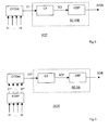
- Fig .2a schematically shows an optical transmitter OT being the transmitting component of an optical transmission system according to the invention.
- the optical transmitter OT comprises an optical time division multiplexing unit OTDM, referred to below as time multiplexer OTDM and a conversion filter CF.
- Four electrical input signals 11 - 14, symbolised as arrows, are each fed to respective input ports of said time multiplexer OTDM.
- One multiplexer output signal Sl or multiplexed signal Sl, symbolised as arrow, that is emitted at the output port of said time multiplexer OTDM, is fed to the input port of the conversion filter CF.
- the optical transmitter output signal SO is emitted.
- the optical time division multiplexing unit OTDM of the optical transmitter OT preferably shows a structure as described above.
- a pulsed optical signal is emitted by a pulsed laser source. This signal is split into a certain number of portions of the same intensity, showing the same, original pulse pattern. Each of these portions is fed into a modulator, each responsive to a data signal with a bit rate, that equals the bit rate of the output optical system divided by the number of branches or modulators.
- the different data signals represent electrical input signals.
- the modulated signals are then recombined at an optical coupler with a certain time lag between each of them to generate the optical output signal with a multiple bit rate compared to bit rate of the input signals.
- the time multiplexer output signal Sl shows a return-to-zero (RZ) like pulse format with a pulse width, that is far smaller than the bit duration time of said multiplexer output signal Sl.
- the conversion filter CF is connected to the output of the optical time multiplexer unit OTDM.
- the conversion filter CF broadens the RZ like pulses of said time multiplexer output signal Sll up to such a pulse width that pulses do not overlap into adjacent time windows or only overlap such, that time channel division at receivers side remains possible.
- the spectral bandwidth of the output signal SO is reduced compared to input signal Sl1 of the conversion filter CF.
- a signal with RZ like pulses is converted to a signal showing NRZ like pulses, i.e. a pulse format, that uses a minimum optical bandwidth.
- the conversion filter CF may be realised as an optical filter with a planar optical structure like cascaded Mach-Zehnder interferometers, as optical transversal filter or as a fiber bragg grating as known in the prior art.
- the most important advantage of a method according to the invention is achieved when using time division multiplexing OTDM methods, often used to gain very high bit rates, in combination with wavelength division multiplexing (WDM) methods, often used in optical core networks or for long distance transmission to exploit fiber capacity.
- WDM wavelength division multiplexing
- WDM transmission
- WDM-signals a certain number of modulated optical carriers with different frequencies
- WDM-signals are simultaneously transmitted in an optical waveguide without significant mutual optical influencing (cross talk) between each other.
- Each optical carrier can be seen as independent wavelength channel or WDM channel.
- WDM channels In current WDM systems with tight channel spacing, so-called dense wavelength-division multiplexing (DWDM) systems, for example, 40 channels are transmitted showing an equidistant frequency spacing of the carrier frequencies of down to 50 GHz.
- DWDM dense wavelength-division multiplexing
- the allowed bandwidth of the corresponding WDM signals is at least limited to the distance between the carrier frequencies; however the allowed bandwidth is further limited to smaller values for reasons of accurate signal discrimination in the frequency domain. To allow high bit rates in each the WDM channels, effective use of bandwidth is necessary.
- Parallel bandwidth reduction of the said signals can be achieved by connecting a conversion filter CF in each optical branch between the different time division multiplexers and said wavelength division multiplexer.
- Fig.2b schematically shows a wavelength division multiplex optical transmitter WOT, further referred to as WDM transmitter WOT.
- the WDM transmitter WOT by way of example comprises two time multiplexers OTDM1 and OTDM2, a wavelength division multiplexer WDM and a WDM conversion filter WCF.
- the two time multiplexers OTDM1 and OTDM2 each shows four input signals l1- 14 respectively 11' - 14'
- Each time multiplexer OTDM1 and OTDM2 emits a first time multiplexer (optical output) signal Sl1 and a second time multiplexer (optical output) signal Sl2 respectively, that are fed to a wavelength division multiplexer WDM.
- the wavelength division multiplexer output signal Sl' is fed to a WDM conversion filter WCF.
- the output of said WDM conversion filter WCF emits an WDM output signal SO'.
- the time multiplexers OTDM1 and OTDM2 combines said input signals I1-14 and I1'- 14' respectively as described under Fig. each by first carrying out an electro-optical conversion of said input signals and then optically combining them to said first time multiplexer signal SI1 and to a second time multiplexer signal Sl2 respectively.
- the carrier signal of each of said time multiplexer signals SI1 and Sl2 shows different frequencies or wavelengths respectively.
- the output signal Sl ' of the WDM multiplexer is fed to the conversion filter WCF, showing a repetitive optical transfer characteristics with a free spectral range (FSR) equal to integers of the WDM channel spacing, e.g. 50 GHz for the above mentioned frequency spacing example, or with a free spectral range (FSR) showing a multiple whole-numbered multiple of the channel spacing like optical lattice filters consisting og Mach-Zehnder interferometers with e.g. 100 GHz or 200 GHz.
- FSR free spectral range
- Fig. 3 schematically shows an exemplary embodiment of a conversion filter CF provided for an optical transmitter according to the invention.
- An optical circulator OZ is shown with an (optical) input port 1, an (optical) intermediate port 2 and an (optical) output port 3.
- An input fiber IF is connected to the input port 1
- a reflection fiber RF is connected to the intermediate port 2
- an output fiber OF is connected to the output port 3.
- the reflection fiber shows a bragg grating BG integrated in the optical waveguide, a so-called in-fiber bragg grating.
- An (optical) input signal Sl is fed to the input fiber IF and an (optical) output signal SO is output by the output fiber OF.
- the circulator OZ is configured in such a way that an optical signal arriving at the input port 1 is dropped again at the intermediate port 2 and an optical signal arriving at the intermediate port 2 is dropped again at the output port 3.
- the input signal Sl proceeds to the input port of the circulator OZ.
- This signal is dropped at the intermediate port 2 into the reflecting fiber RF.
- the bragg grating BG operates in a reflecting mode.
- the bragg grating BG is constructed such, that only a part of the irradiated signal is reflected back to the intermediate port 2 depending on the frequency, with an amplitude and a phase spectrum according to the transfer function of the filter CF.
- This signal then is dropped at the output port 3 forming the output signal SO.
- the output signal SO shows an expansion of its pulses in the time domain.
- the conversion filter CF according to Fig.3 can be applied both to an optical transmitter OT according to the invention and a wavelength division multiplex optical transmitter WOT according to the invention.
- the free spectral range (FSR) must be equal to the WDM frequency spacing or of an integer multiple of the WDM frequency spacing.
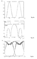
- FIG.4a - Fig.4c show simulation results with a conversion filter CF according to Fig.3.
- Fig.4a shows an eye diagram with an exemplary RZ modulation pulse format of an optically multiplexed optical signal as input signal Sl of a conversion filter CF.
- a normalised time T is marked running from 0 to 2, representing two bit periods of the input signal Sl.
- a normalised amplitude A is marked, running from 0 to 1.
- the eye representation shows, that the input signal Sl after each pulse returns to zero, not regarding whether an optical pulse will follow in the next bit period or not.
- the pulse width is quite narrow, e.g. less than 50 % of the available bit time window regarding the 0.5-level of the normalised amplitude A.
- Fig.4b shows a diagram with a schematic exemplary transfer function curve or filter response of a conversion filter CF.
- a phase filter response and in the lower part, an amplitude filter response is shown.
- a frequency F is marked running from -1 to 1, to be multiplied by a factor 1 exp 11.
- a logarithmic amplitude ADB is marked, running from -20 to 0.
- the amplitude response shows one main lobe in the frequency center and two smaller side lobes each to the left and the right side of the mail lobe.
- the phase PH In the area of the mail lobe, the phase PH equals zero. In the areas of the side lobes, the phase PH equals pi (3,14157), i.e. the transfer function in these areas shows negative values.
- the si-function represents a rectangle impulse.
- the output pulse of a conversion filter CF is determined by a time domain convolution of the input signal with said filter response, narrow pulses of an input signal Sl are broadened in the output signal.
- the time delay, that is accompanied by said filtering is not relevant here and thus is not further regarded.
- Fig.4c shows an eye diagram of an output signal SO of the conversion filter CF described under Fig.4b, fed by a signal described under Fig.4a.
- a normalised time T is marked running from 0 to 2, representing two bit periods of the output signal Sl.
- a normalised amplitude A is marked, running from 0 to 1.
- the eye representation shows, that the pulse width of the output signal SO is significantly broader the pulse format of the input signal Sl, e.g. more than 80 % of the available bit time window regarding the 0.5-level of the normalised amplitude A.
- the pulses of two subsequent bit periods of the output signal SO generated by an inventive transmitter partly overlap just such, that said signal SO does not return to zero between said pulses.
- the bandwidth of the output signal SO thus is significantly smaller than the bandwidth of the input signal Sl.
- Fig.5 schematically shows a vestigial side band optical transmitter VOT according to the invention, comprising, by way of example, the optical time division multiplexing unit OTDM and the conversion filter CF as shown in Fig.2a.
- four electrical input signals I1 - I4 are fed to respective input ports of the optical time division multiplexing unit OTDM and the multiplexed signal Sl, emitted at the output port of said time multiplexer OTDM, is fed to the input port of the conversion filter CF.
- the output port of said conversion Filter CF providing the output signal SO is connected to an additionally provided vestigial side band filter VSBF compared to Fig.2a.
- the output of said vestigial side band filter VSBF provides the vestigial side band output signal SVSB.
- the conversion filter CF and the vestigial side band filter VSBF connected together in series, form a first modified filter RZ-VSB.
- the conversion filter CF transforming return-to-zero signals to non-return-to-zero signals reduces the signal bandwidth of the filter output signal SO as described above.
- the vestigial side band filter VSBF cuts one of the two side bands of the received signal SO and thus further reduces the bandwidth of respective vestigial side band output signal SVSB compared to the multiplexed signal Sl.
- the vestigial side band filter VSBF allows for reducing the bandwidth of the respectively received signal SO to the half.
- the bandwidth of the multiplexed signal Sl is reduced in two stages.
- the first modified filter RZ-VSB is realised as single optical filter, the transfer characteristics of which are corresponding to the transfer characteristics of the described filters connected in series, i.e. the optical functionalities of each of both filters CF and VSBF are performed by said single optical filter.
- Fig.6 schematically shows a duobinary optical transmitter DOT according to the invention, comprising, by way of example, the optical time division multiplexing unit OTDM and the conversion filter CF as shown in Fig.2a. Additionally an electrical duobinary precoder EDBP and a duobinary filter DBF are shown. The four electrical input signals I1- I4 known from Fig.2a are fed to the electrical duobinary precoder EDBP. Said electrical duobinary precoder EDBP generates precoded input signals I1*- I4* that are fed to the input ports of the optical time division multiplexing unit OTDM.
- the output port of said conversion Filter CF, providing the precoded output signal SO* is connected to the duobinary filter DBF.
- the output of said duobinary filter DBF provides the duobinary output signal SDB.
- the conversion filter CF and the duobinary filter DBF connected together in series, form a second modified filter RZ-DB.
- the conversion filter CF reduces the bandwidth of the received multiplexed signal Sl as described before.
- the precoded multiplexed signal SI* shows two different discrete intensity values (representing the possible bit values "0" and "1").
- the duobinary coder or duo binary filter DBF generates a tree intensity value signal SDB e.g. splitting the received signal SO* into two signals SO*, time delaying one of these signals SO* to the duration of one bit slot and adding or coupling the delayed signal and the non delayed signal.
- the generated duobinary signals SDB requires less bandwidth than the comparable NRZ signal SO*.
- the original electrical input signals are electrically precoded by the electrical duobinary precoder EDBP.
- the precoder may comprise a feed back loop as known from the prior art.
- the precoder may be realized using standard logic integrated circuits.
- the second modified filter RZ-DB is realised as single optical filter with transfer characteristics similar to the transfer characteristics of the described filters CF and DBF connected in series.
- a further embodiment of the invention concerns the integration of a WDM conversion filter WCF into a WDM multiplexer or WDM demultiplexer e.g. realised as arrayed wave guide.
- WDM multiplexer or WDM demultiplexer e.g. realised as arrayed wave guide.
- RZ like signals can be multiplexed and converted to NRZ like signals at the same time.
Landscapes
- Engineering & Computer Science (AREA)
- Computer Networks & Wireless Communication (AREA)
- Signal Processing (AREA)
- Physics & Mathematics (AREA)
- Electromagnetism (AREA)
- Optical Communication System (AREA)
Abstract
Description
- Fig.1
- schematically shows an optical transmission system according to the invention comprising an optical transmitter according to the invention, an optical transmission line and an optical receiver,
- Fig.2a
- schematically shows an optical transmitter with a single optical carrier at its output according to the invention,
- Fig.2b
- schematically shows an optical transmitter for a WDM system according to the invention,
- Fig.3
- schematically shows an exemplary embodiment of a conversion filter provided for an optical transmitter according to the invention,
- Fig.4a
- shows a diagram with an exemplary modulation pulse format of a multiplexed optical signal at the input of a conversion filter according to Fig.3,
- Fig.4b
- shows a diagram with an exemplary transfer function curve of a conversion filter according to Fig.3,
- Fig.4c
- shows a diagram with an exemplary optical eye pattern of an output signal of a conversion filter output according to Fig.3,
- Fig.5
- shows an optical transmitter according to the invention with a vestigial side band filter and
- Fig.6
- shows an optical transmitter according to the invention with a duobinary filter.
Claims (9)
- An optical transmitter (OT, WOT) for transmitting signals with high data rates, comprising at least one optical signal source for generating a return-to-zero like pulse signal, characterised in, that further a conversion filter (CF, WCF) at the output of the optical transmitter (OT, WOT) is comprised, wherein the conversion filter (CF, WCF) shows filter means for generating an optical output signal (SO, SO') with broadened pulses for reducing the use of spectral bandwidth.
- An optical transmitter (OT, WOT) according to claim 1, characterised in, that said at least one optical signal source is realised by at least one corresponding optical time division multiplexer (OTDM) and each optical time division multiplexer (OTDM) is realised such, that a corresponding return-to-zero like pulse multiplexed signal (Sl, Sl') is generated out of at least two input signals (11, 12).
- An optical transmitter (WOT) according to claim 2, characterised in, that two or more time division multiplexers (OTDM1, OTDM2) and a wavelength division multiplexer (WDMU) are comprised, wherein the wavelength division multiplexer (WDMU) shows at least two optical inputs to combine the optical output signals (Sl1, Sl2) of said time division multiplexers (OTDM1, OTDM2) to generate a time and wavelength multiplexed signal (Sl') with a defined frequency spacing, and that the conversion filter (WCF) for reducing the use of spectral bandwidth of the time and wavelength division multiplexed signal (Sl') is a frequency repetitive conversion filter (WCF) showing a free spectral range corresponding to said defined frequency spacing.
- An optical transmitter (OT) according to claim 1, characterized in, that the filter means of the conversion filter (CF) are realised such, that return-to-zero like pulses of the time division multiplexer output signal (Sl) are converted into non-return-to-zero like pulses.
- An optical transmitter (VOT) according to claim 1, characterized in, that an optical vestigial side band filter (VSBF) is comprised connected in series behind the conversion filter (CF).
- An optical transmitter (DOT) according to claim 1, characterized in, that that an optical duo binary filter (DBF) is comprised connected in series to the conversion filter (CF).
- An optical transmitter (DOT) according to claim 5, characterized in, that that an electrical duobinary precoder (EDBP) is comprised with means to precode the electrical input signals (11, 12) such, that an error propagation of a decoding error at receivers side can be avoided.
- An optical transmission system with an optical transmitter (OT), an optical transmission link (OF) and an optical receiver (OR), wherein the optical transmitter comprises an optical time division multiplexer (OTDM) for generating a multiplexed signal (Sl) out of at least two input signals (I1, 12) characterised in, that the optical transmitter (OT) further comprises a conversion filter (CF) for compressing or reducing the spectral bandwidth of the multiplexed signal (Sl).
- A method to generate an optical output signal (SO, SO') by optically time multiplexing at least two input signals (I1, 12) to a multiplexed signal (Sl, Sl')/ characterized in, that the bandwidth of said multiplexed signal (Sl, Sl') is compressed or reduced to obtain an output signal (SO, SO') with a reduced use of optical bandwidth compared to the use of optical bandwidth of said multiplexed signal (Sl, Sl').
Priority Applications (5)
| Application Number | Priority Date | Filing Date | Title |
|---|---|---|---|
| AT02360077T ATE260002T1 (en) | 2002-03-04 | 2002-03-04 | OPTICAL TRANSMITTER, SYSTEM AND METHOD FOR TRANSMITTING SIGNALS WITH HIGH DATA RATES |
| DE60200221T DE60200221T2 (en) | 2002-03-04 | 2002-03-04 | Optical transmitter, system and method for transmitting signals with high data rates |
| EP02360077A EP1345342B1 (en) | 2002-03-04 | 2002-03-04 | An optical transmitter for transmitting signals with high data rates, an optical transmission system and a method therefor |
| US10/368,628 US20030165341A1 (en) | 2002-03-04 | 2003-02-20 | Optical transmitter for transmitting signals with high data rates, an optical transmission system and a method therefore |
| CN03104991.5A CN1220347C (en) | 2002-03-04 | 2003-02-28 | Optical transmitter optical transmission system and method used for high data speed transmission signal |
Applications Claiming Priority (1)
| Application Number | Priority Date | Filing Date | Title |
|---|---|---|---|
| EP02360077A EP1345342B1 (en) | 2002-03-04 | 2002-03-04 | An optical transmitter for transmitting signals with high data rates, an optical transmission system and a method therefor |
Publications (2)
| Publication Number | Publication Date |
|---|---|
| EP1345342A1 true EP1345342A1 (en) | 2003-09-17 |
| EP1345342B1 EP1345342B1 (en) | 2004-02-18 |
Family
ID=27763464
Family Applications (1)
| Application Number | Title | Priority Date | Filing Date |
|---|---|---|---|
| EP02360077A Expired - Lifetime EP1345342B1 (en) | 2002-03-04 | 2002-03-04 | An optical transmitter for transmitting signals with high data rates, an optical transmission system and a method therefor |
Country Status (5)
| Country | Link |
|---|---|
| US (1) | US20030165341A1 (en) |
| EP (1) | EP1345342B1 (en) |
| CN (1) | CN1220347C (en) |
| AT (1) | ATE260002T1 (en) |
| DE (1) | DE60200221T2 (en) |
Families Citing this family (9)
| Publication number | Priority date | Publication date | Assignee | Title |
|---|---|---|---|---|
| FR2844654B1 (en) * | 2002-09-12 | 2005-02-25 | Cit Alcatel | FREQUENCY COMB FOR OPTICAL FREQUENCY DIVISION MULTIPLEXING NETWORK |
| GB0308951D0 (en) * | 2003-04-17 | 2003-05-28 | Azea Networks Ltd | Top-flat spectrum data format for Nx40 Gbit/s WDM transmission with 0.8 bit/s/Hz spectral efficiency |
| KR100547781B1 (en) * | 2003-06-10 | 2006-01-31 | 삼성전자주식회사 | Polarized Duobinary Optical Transmission Device |
| FR2892581B1 (en) * | 2005-10-21 | 2008-01-04 | Alcatel Sa | HIGH SPEED MULTIPLEXER WITH PARALLEL ARCHITECTURE |
| US7706420B2 (en) * | 2006-09-05 | 2010-04-27 | Corning Incorporated | Optical power modulation at high frequency |
| US20080082085A1 (en) * | 2006-09-08 | 2008-04-03 | Krasutsky Nicholas J | Time division multiplexed, beam combining for laser signal generation |
| US8238757B2 (en) * | 2007-01-18 | 2012-08-07 | Futurewei Technologies, Inc. | Method and apparatus for generating optical duobinary signals with enhanced receiver sensitivity and spectral efficiency |
| CN106533564B (en) * | 2016-11-25 | 2019-04-05 | 通号工程局集团北京研究设计实验中心有限公司 | A kind of multi-wavelength digital optical communication system based on Wavelength-encoding |
| US11540443B2 (en) * | 2019-01-31 | 2023-01-03 | Deere & Company | System and method for measurement of harvested material in a cleaning assembly |
Citations (4)
| Publication number | Priority date | Publication date | Assignee | Title |
|---|---|---|---|---|
| US5926297A (en) * | 1996-09-03 | 1999-07-20 | Fujitsu Limited | Optical modulating device and optical modulating method |
| EP1041783A2 (en) * | 1999-04-01 | 2000-10-04 | Nortel Networks Limited | Encoding, modulation and multiplexing for optical transmission |
| US6141129A (en) * | 1997-12-18 | 2000-10-31 | Lucent Technologies Inc. | Method and apparatus for all-optical data regeneration |
| EP1143643A2 (en) * | 2000-01-12 | 2001-10-10 | Alcatel | An optical transmission system |
Family Cites Families (8)
| Publication number | Priority date | Publication date | Assignee | Title |
|---|---|---|---|---|
| US6195484B1 (en) * | 1997-10-02 | 2001-02-27 | 3M Innovative Properties Company | Method and apparatus for arbitrary spectral shaping of an optical pulse |
| AU3881199A (en) * | 1998-05-08 | 1999-11-29 | University Of Michigan, The | Soliton pulse transmission over waveguide fiber lengths |
| US6289151B1 (en) * | 1998-10-30 | 2001-09-11 | Lucent Technologies Inc. | All-pass optical filters |
| JP3721062B2 (en) * | 2000-08-30 | 2005-11-30 | 日本電信電話株式会社 | Optical transmitter |
| US6490069B1 (en) * | 2001-01-29 | 2002-12-03 | Stratalight Communications, Inc. | Transmission and reception of duobinary multilevel pulse-amplitude-modulated optical signals using subtraction-based encoder |
| JP4801281B2 (en) * | 2001-05-31 | 2011-10-26 | 富士通株式会社 | Optical pulse insertion device |
| US7035538B2 (en) * | 2001-07-09 | 2006-04-25 | University Of Southern California | Monitoring optical dispersion based on vestigial side band optical filtering |
| US6956989B2 (en) * | 2002-12-18 | 2005-10-18 | Agilent Technologies, Inc. | Method and system for generating low jitter NRZ optical data utilizing an optical pulse stretcher |
-
2002
- 2002-03-04 DE DE60200221T patent/DE60200221T2/en not_active Expired - Lifetime
- 2002-03-04 EP EP02360077A patent/EP1345342B1/en not_active Expired - Lifetime
- 2002-03-04 AT AT02360077T patent/ATE260002T1/en not_active IP Right Cessation
-
2003
- 2003-02-20 US US10/368,628 patent/US20030165341A1/en not_active Abandoned
- 2003-02-28 CN CN03104991.5A patent/CN1220347C/en not_active Expired - Lifetime
Patent Citations (4)
| Publication number | Priority date | Publication date | Assignee | Title |
|---|---|---|---|---|
| US5926297A (en) * | 1996-09-03 | 1999-07-20 | Fujitsu Limited | Optical modulating device and optical modulating method |
| US6141129A (en) * | 1997-12-18 | 2000-10-31 | Lucent Technologies Inc. | Method and apparatus for all-optical data regeneration |
| EP1041783A2 (en) * | 1999-04-01 | 2000-10-04 | Nortel Networks Limited | Encoding, modulation and multiplexing for optical transmission |
| EP1143643A2 (en) * | 2000-01-12 | 2001-10-10 | Alcatel | An optical transmission system |
Non-Patent Citations (2)
| Title |
|---|
| BIGO S ET AL: "MULTI-TERABIT/S TRANSMISSION OVER ALCATEL TERALIGHTTM FIBER", ELECTRICAL COMMUNICATION, ALCATEL. BRUSSELS, BE, no. 4, 1 October 2000 (2000-10-01), pages 288 - 296, XP000976732, ISSN: 0013-4252 * |
| NAVARRO J A ET AL: "Direct-modulation/direct-detection technology in multigigabit optical networks", ELECTROTECHNICAL CONFERENCE, 1994. PROCEEDINGS., 7TH MEDITERRANEAN ANTALYA, TURKEY 12-14 APRIL 1994, NEW YORK, NY, USA,IEEE, 12 April 1994 (1994-04-12), pages 175 - 178, XP010130833, ISBN: 0-7803-1772-6 * |
Also Published As
| Publication number | Publication date |
|---|---|
| ATE260002T1 (en) | 2004-03-15 |
| CN1220347C (en) | 2005-09-21 |
| US20030165341A1 (en) | 2003-09-04 |
| CN1442975A (en) | 2003-09-17 |
| DE60200221T2 (en) | 2004-07-08 |
| DE60200221D1 (en) | 2004-03-25 |
| EP1345342B1 (en) | 2004-02-18 |
Similar Documents
| Publication | Publication Date | Title |
|---|---|---|
| EP1060589B1 (en) | Method and apparatus for improving spectral efficiency in wavelength division multiplexed transmission systems | |
| CA2183912C (en) | Chirped-pulse multiple wavelength communications system | |
| CA2132559C (en) | High-density optical wavelength division multiplexing | |
| US7340182B2 (en) | Multiplexer | |
| US7627253B1 (en) | RF-photonic transversal filter method and apparatus | |
| EP1304819A2 (en) | Central multi-wavelength source | |
| KR0157429B1 (en) | Optimized wavelength-division-multiplexed lightwave communication system | |
| EP1083685B1 (en) | Optical signal generating circuit and optical transmission line | |
| US7197251B2 (en) | Optical phase modulation | |
| KR20010043970A (en) | Multiwavelength mode-locked dense wavelength division multiplexed optical communication systems | |
| JP2003298525A (en) | Optical single side band transmitter | |
| EP1345342B1 (en) | An optical transmitter for transmitting signals with high data rates, an optical transmission system and a method therefor | |
| JPH09214427A (en) | Method for reducing influence of optical beat interruption and optical wave signal transmission system | |
| US6496297B1 (en) | Device and method for modulating an optical signal | |
| US6430336B1 (en) | Device and method for minimizing optical channel drift | |
| EP1436919B1 (en) | Optical signal transmission | |
| Moscoso-Mártir et al. | Silicon photonics DWDM NLFT soliton transmitter implementation and link budget assessment | |
| JP4622785B2 (en) | Optical code division multiplexing transmitter | |
| US6172781B1 (en) | Wave division multiplexed optical network | |
| EP1396950A2 (en) | Optical transmission system, optical transmitter and methods thereof | |
| US6751416B2 (en) | Reconfigurable optical recognition of bit information in a digital data stream with different bit rates | |
| JP2005094287A (en) | Optical transmission and reception method and system, and optical transmission method and apparatus | |
| EP1618691B1 (en) | Data format for high bit rate wdm transmission | |
| EP1408633A1 (en) | Apparatus and method for regeneration of optical pulses | |
| JP3953934B2 (en) | Code conversion circuit and optical transmission circuit |
Legal Events
| Date | Code | Title | Description |
|---|---|---|---|
| PUAI | Public reference made under article 153(3) epc to a published international application that has entered the european phase |
Free format text: ORIGINAL CODE: 0009012 |
|
| GRAP | Despatch of communication of intention to grant a patent |
Free format text: ORIGINAL CODE: EPIDOSNIGR1 |
|
| 17P | Request for examination filed |
Effective date: 20021030 |
|
| AK | Designated contracting states |
Kind code of ref document: A1 Designated state(s): AT BE CH CY DE DK ES FI FR GB GR IE IT LI LU MC NL PT SE TR |
|
| AX | Request for extension of the european patent |
Extension state: AL LT LV MK RO SI |
|
| GRAS | Grant fee paid |
Free format text: ORIGINAL CODE: EPIDOSNIGR3 |
|
| GRAA | (expected) grant |
Free format text: ORIGINAL CODE: 0009210 |
|
| AK | Designated contracting states |
Kind code of ref document: B1 Designated state(s): AT BE CH CY DE DK ES FI FR GB GR IE IT LI LU MC NL PT SE TR |
|
| AX | Request for extension of the european patent |
Extension state: AL LT LV MK RO SI |
|
| PG25 | Lapsed in a contracting state [announced via postgrant information from national office to epo] |
Ref country code: NL Free format text: LAPSE BECAUSE OF FAILURE TO SUBMIT A TRANSLATION OF THE DESCRIPTION OR TO PAY THE FEE WITHIN THE PRESCRIBED TIME-LIMIT Effective date: 20040218 Ref country code: CY Free format text: LAPSE BECAUSE OF FAILURE TO SUBMIT A TRANSLATION OF THE DESCRIPTION OR TO PAY THE FEE WITHIN THE PRESCRIBED TIME-LIMIT Effective date: 20040218 Ref country code: CH Free format text: LAPSE BECAUSE OF FAILURE TO SUBMIT A TRANSLATION OF THE DESCRIPTION OR TO PAY THE FEE WITHIN THE PRESCRIBED TIME-LIMIT Effective date: 20040218 Ref country code: LI Free format text: LAPSE BECAUSE OF FAILURE TO SUBMIT A TRANSLATION OF THE DESCRIPTION OR TO PAY THE FEE WITHIN THE PRESCRIBED TIME-LIMIT Effective date: 20040218 Ref country code: FI Free format text: LAPSE BECAUSE OF FAILURE TO SUBMIT A TRANSLATION OF THE DESCRIPTION OR TO PAY THE FEE WITHIN THE PRESCRIBED TIME-LIMIT Effective date: 20040218 Ref country code: BE Free format text: LAPSE BECAUSE OF FAILURE TO SUBMIT A TRANSLATION OF THE DESCRIPTION OR TO PAY THE FEE WITHIN THE PRESCRIBED TIME-LIMIT Effective date: 20040218 Ref country code: TR Free format text: LAPSE BECAUSE OF FAILURE TO SUBMIT A TRANSLATION OF THE DESCRIPTION OR TO PAY THE FEE WITHIN THE PRESCRIBED TIME-LIMIT Effective date: 20040218 Ref country code: AT Free format text: LAPSE BECAUSE OF FAILURE TO SUBMIT A TRANSLATION OF THE DESCRIPTION OR TO PAY THE FEE WITHIN THE PRESCRIBED TIME-LIMIT Effective date: 20040218 |
|
| REG | Reference to a national code |
Ref country code: GB Ref legal event code: FG4D |
|
| REG | Reference to a national code |
Ref country code: CH Ref legal event code: EP |
|
| PG25 | Lapsed in a contracting state [announced via postgrant information from national office to epo] |
Ref country code: IE Free format text: LAPSE BECAUSE OF NON-PAYMENT OF DUE FEES Effective date: 20040304 Ref country code: LU Free format text: LAPSE BECAUSE OF NON-PAYMENT OF DUE FEES Effective date: 20040304 |
|
| REG | Reference to a national code |
Ref country code: IE Ref legal event code: FG4D |
|
| REF | Corresponds to: |
Ref document number: 60200221 Country of ref document: DE Date of ref document: 20040325 Kind code of ref document: P |
|
| PG25 | Lapsed in a contracting state [announced via postgrant information from national office to epo] |
Ref country code: MC Free format text: LAPSE BECAUSE OF NON-PAYMENT OF DUE FEES Effective date: 20040331 |
|
| PG25 | Lapsed in a contracting state [announced via postgrant information from national office to epo] |
Ref country code: DK Free format text: LAPSE BECAUSE OF FAILURE TO SUBMIT A TRANSLATION OF THE DESCRIPTION OR TO PAY THE FEE WITHIN THE PRESCRIBED TIME-LIMIT Effective date: 20040518 Ref country code: GR Free format text: LAPSE BECAUSE OF FAILURE TO SUBMIT A TRANSLATION OF THE DESCRIPTION OR TO PAY THE FEE WITHIN THE PRESCRIBED TIME-LIMIT Effective date: 20040518 Ref country code: SE Free format text: LAPSE BECAUSE OF FAILURE TO SUBMIT A TRANSLATION OF THE DESCRIPTION OR TO PAY THE FEE WITHIN THE PRESCRIBED TIME-LIMIT Effective date: 20040518 |
|
| PG25 | Lapsed in a contracting state [announced via postgrant information from national office to epo] |
Ref country code: ES Free format text: LAPSE BECAUSE OF FAILURE TO SUBMIT A TRANSLATION OF THE DESCRIPTION OR TO PAY THE FEE WITHIN THE PRESCRIBED TIME-LIMIT Effective date: 20040529 |
|
| AKX | Designation fees paid |
Designated state(s): AT BE CH CY DE DK ES FI FR GB GR IE IT LI LU MC NL PT SE TR |
|
| LTIE | Lt: invalidation of european patent or patent extension |
Effective date: 20040218 |
|
| NLV1 | Nl: lapsed or annulled due to failure to fulfill the requirements of art. 29p and 29m of the patents act | ||
| REG | Reference to a national code |
Ref country code: CH Ref legal event code: PL |
|
| ET | Fr: translation filed | ||
| PLBE | No opposition filed within time limit |
Free format text: ORIGINAL CODE: 0009261 |
|
| STAA | Information on the status of an ep patent application or granted ep patent |
Free format text: STATUS: NO OPPOSITION FILED WITHIN TIME LIMIT |
|
| REG | Reference to a national code |
Ref country code: IE Ref legal event code: MM4A |
|
| 26N | No opposition filed |
Effective date: 20041119 |
|
| PG25 | Lapsed in a contracting state [announced via postgrant information from national office to epo] |
Ref country code: PT Free format text: LAPSE BECAUSE OF NON-PAYMENT OF DUE FEES Effective date: 20040718 |
|
| REG | Reference to a national code |
Ref country code: GB Ref legal event code: 732E Free format text: REGISTERED BETWEEN 20131114 AND 20131120 |
|
| REG | Reference to a national code |
Ref country code: FR Ref legal event code: GC Effective date: 20140717 |
|
| REG | Reference to a national code |
Ref country code: FR Ref legal event code: RG Effective date: 20141016 |
|
| REG | Reference to a national code |
Ref country code: FR Ref legal event code: PLFP Year of fee payment: 14 |
|
| REG | Reference to a national code |
Ref country code: FR Ref legal event code: PLFP Year of fee payment: 15 |
|
| REG | Reference to a national code |
Ref country code: FR Ref legal event code: PLFP Year of fee payment: 16 |
|
| REG | Reference to a national code |
Ref country code: FR Ref legal event code: PLFP Year of fee payment: 17 |
|
| REG | Reference to a national code |
Ref country code: DE Ref legal event code: R082 Ref document number: 60200221 Country of ref document: DE Representative=s name: METACOM LEGAL, DE Ref country code: DE Ref legal event code: R082 Ref document number: 60200221 Country of ref document: DE Representative=s name: BARKHOFF REIMANN VOSSIUS, DE Ref country code: DE Ref legal event code: R081 Ref document number: 60200221 Country of ref document: DE Owner name: WSOU INVESTMENTS, LLC, LOS ANGELES, US Free format text: FORMER OWNER: ALCATEL LUCENT, PARIS, FR |
|
| PGFP | Annual fee paid to national office [announced via postgrant information from national office to epo] |
Ref country code: IT Payment date: 20200423 Year of fee payment: 19 |
|
| REG | Reference to a national code |
Ref country code: GB Ref legal event code: 732E Free format text: REGISTERED BETWEEN 20201022 AND 20201028 |
|
| PGFP | Annual fee paid to national office [announced via postgrant information from national office to epo] |
Ref country code: FR Payment date: 20210825 Year of fee payment: 20 |
|
| PGFP | Annual fee paid to national office [announced via postgrant information from national office to epo] |
Ref country code: DE Payment date: 20210827 Year of fee payment: 20 Ref country code: GB Payment date: 20210827 Year of fee payment: 20 |
|
| REG | Reference to a national code |
Ref country code: DE Ref legal event code: R082 Ref document number: 60200221 Country of ref document: DE Representative=s name: METACOM LEGAL, DE |
|
| REG | Reference to a national code |
Ref country code: DE Ref legal event code: R071 Ref document number: 60200221 Country of ref document: DE |
|
| REG | Reference to a national code |
Ref country code: GB Ref legal event code: PE20 Expiry date: 20220303 |
|
| PG25 | Lapsed in a contracting state [announced via postgrant information from national office to epo] |
Ref country code: IT Free format text: LAPSE BECAUSE OF NON-PAYMENT OF DUE FEES Effective date: 20210304 Ref country code: GB Free format text: LAPSE BECAUSE OF EXPIRATION OF PROTECTION Effective date: 20220303 |