EP2704185A1 - Method for producing electronic component module and electronic component module - Google Patents
Method for producing electronic component module and electronic component module Download PDFInfo
- Publication number
- EP2704185A1 EP2704185A1 EP12775989.2A EP12775989A EP2704185A1 EP 2704185 A1 EP2704185 A1 EP 2704185A1 EP 12775989 A EP12775989 A EP 12775989A EP 2704185 A1 EP2704185 A1 EP 2704185A1
- Authority
- EP
- European Patent Office
- Prior art keywords
- electronic component
- bumps
- center
- bare
- plural
- Prior art date
- Legal status (The legal status is an assumption and is not a legal conclusion. Google has not performed a legal analysis and makes no representation as to the accuracy of the status listed.)
- Withdrawn
Links
Images



Classifications
-
- H—ELECTRICITY
- H05—ELECTRIC TECHNIQUES NOT OTHERWISE PROVIDED FOR
- H05K—PRINTED CIRCUITS; CASINGS OR CONSTRUCTIONAL DETAILS OF ELECTRIC APPARATUS; MANUFACTURE OF ASSEMBLAGES OF ELECTRICAL COMPONENTS
- H05K1/00—Printed circuits
- H05K1/18—Printed circuits structurally associated with non-printed electric components
- H05K1/181—Printed circuits structurally associated with non-printed electric components associated with surface mounted components
-
- H—ELECTRICITY
- H05—ELECTRIC TECHNIQUES NOT OTHERWISE PROVIDED FOR
- H05K—PRINTED CIRCUITS; CASINGS OR CONSTRUCTIONAL DETAILS OF ELECTRIC APPARATUS; MANUFACTURE OF ASSEMBLAGES OF ELECTRICAL COMPONENTS
- H05K13/00—Apparatus or processes specially adapted for manufacturing or adjusting assemblages of electric components
- H05K13/04—Mounting of components, e.g. of leadless components
- H05K13/046—Surface mounting
- H05K13/0465—Surface mounting by soldering
-
- H—ELECTRICITY
- H05—ELECTRIC TECHNIQUES NOT OTHERWISE PROVIDED FOR
- H05K—PRINTED CIRCUITS; CASINGS OR CONSTRUCTIONAL DETAILS OF ELECTRIC APPARATUS; MANUFACTURE OF ASSEMBLAGES OF ELECTRICAL COMPONENTS
- H05K3/00—Apparatus or processes for manufacturing printed circuits
- H05K3/30—Assembling printed circuits with electric components, e.g. with resistors
- H05K3/32—Assembling printed circuits with electric components, e.g. with resistors electrically connecting electric components or wires to printed circuits
- H05K3/34—Assembling printed circuits with electric components, e.g. with resistors electrically connecting electric components or wires to printed circuits by soldering
- H05K3/341—Surface mounted components
-
- H—ELECTRICITY
- H10—SEMICONDUCTOR DEVICES; ELECTRIC SOLID-STATE DEVICES NOT OTHERWISE PROVIDED FOR
- H10W—GENERIC PACKAGES, INTERCONNECTIONS, CONNECTORS OR OTHER CONSTRUCTIONAL DETAILS OF DEVICES COVERED BY CLASS H10
- H10W70/00—Package substrates; Interposers; Redistribution layers [RDL]
- H10W70/60—Insulating or insulated package substrates; Interposers; Redistribution layers
- H10W70/62—Insulating or insulated package substrates; Interposers; Redistribution layers characterised by their interconnections
- H10W70/65—Shapes or dispositions of interconnections
-
- H—ELECTRICITY
- H10—SEMICONDUCTOR DEVICES; ELECTRIC SOLID-STATE DEVICES NOT OTHERWISE PROVIDED FOR
- H10W—GENERIC PACKAGES, INTERCONNECTIONS, CONNECTORS OR OTHER CONSTRUCTIONAL DETAILS OF DEVICES COVERED BY CLASS H10
- H10W70/00—Package substrates; Interposers; Redistribution layers [RDL]
- H10W70/60—Insulating or insulated package substrates; Interposers; Redistribution layers
- H10W70/62—Insulating or insulated package substrates; Interposers; Redistribution layers characterised by their interconnections
- H10W70/65—Shapes or dispositions of interconnections
- H10W70/652—Cross-sectional shapes
-
- H—ELECTRICITY
- H10—SEMICONDUCTOR DEVICES; ELECTRIC SOLID-STATE DEVICES NOT OTHERWISE PROVIDED FOR
- H10W—GENERIC PACKAGES, INTERCONNECTIONS, CONNECTORS OR OTHER CONSTRUCTIONAL DETAILS OF DEVICES COVERED BY CLASS H10
- H10W70/00—Package substrates; Interposers; Redistribution layers [RDL]
- H10W70/60—Insulating or insulated package substrates; Interposers; Redistribution layers
- H10W70/67—Insulating or insulated package substrates; Interposers; Redistribution layers characterised by their insulating layers or insulating parts
- H10W70/688—Flexible insulating substrates
-
- H—ELECTRICITY
- H10—SEMICONDUCTOR DEVICES; ELECTRIC SOLID-STATE DEVICES NOT OTHERWISE PROVIDED FOR
- H10W—GENERIC PACKAGES, INTERCONNECTIONS, CONNECTORS OR OTHER CONSTRUCTIONAL DETAILS OF DEVICES COVERED BY CLASS H10
- H10W72/00—Interconnections or connectors in packages
- H10W72/90—Bond pads, in general
-
- H—ELECTRICITY
- H10—SEMICONDUCTOR DEVICES; ELECTRIC SOLID-STATE DEVICES NOT OTHERWISE PROVIDED FOR
- H10W—GENERIC PACKAGES, INTERCONNECTIONS, CONNECTORS OR OTHER CONSTRUCTIONAL DETAILS OF DEVICES COVERED BY CLASS H10
- H10W74/00—Encapsulations, e.g. protective coatings
- H10W74/10—Encapsulations, e.g. protective coatings characterised by their shape or disposition
- H10W74/111—Encapsulations, e.g. protective coatings characterised by their shape or disposition the semiconductor body being completely enclosed
- H10W74/127—Encapsulations, e.g. protective coatings characterised by their shape or disposition the semiconductor body being completely enclosed characterised by arrangements for sealing or adhesion
-
- H—ELECTRICITY
- H10—SEMICONDUCTOR DEVICES; ELECTRIC SOLID-STATE DEVICES NOT OTHERWISE PROVIDED FOR
- H10W—GENERIC PACKAGES, INTERCONNECTIONS, CONNECTORS OR OTHER CONSTRUCTIONAL DETAILS OF DEVICES COVERED BY CLASS H10
- H10W90/00—Package configurations
- H10W90/701—Package configurations characterised by the relative positions of pads or connectors relative to package parts
-
- H—ELECTRICITY
- H05—ELECTRIC TECHNIQUES NOT OTHERWISE PROVIDED FOR
- H05K—PRINTED CIRCUITS; CASINGS OR CONSTRUCTIONAL DETAILS OF ELECTRIC APPARATUS; MANUFACTURE OF ASSEMBLAGES OF ELECTRICAL COMPONENTS
- H05K2203/00—Indexing scheme relating to apparatus or processes for manufacturing printed circuits covered by H05K3/00
- H05K2203/02—Details related to mechanical or acoustic processing, e.g. drilling, punching, cutting, using ultrasound
- H05K2203/0278—Flat pressure, e.g. for connecting terminals with anisotropic conductive adhesive
-
- H—ELECTRICITY
- H05—ELECTRIC TECHNIQUES NOT OTHERWISE PROVIDED FOR
- H05K—PRINTED CIRCUITS; CASINGS OR CONSTRUCTIONAL DETAILS OF ELECTRIC APPARATUS; MANUFACTURE OF ASSEMBLAGES OF ELECTRICAL COMPONENTS
- H05K3/00—Apparatus or processes for manufacturing printed circuits
- H05K3/30—Assembling printed circuits with electric components, e.g. with resistors
- H05K3/32—Assembling printed circuits with electric components, e.g. with resistors electrically connecting electric components or wires to printed circuits
- H05K3/34—Assembling printed circuits with electric components, e.g. with resistors electrically connecting electric components or wires to printed circuits by soldering
- H05K3/3465—Application of solder
-
- H—ELECTRICITY
- H10—SEMICONDUCTOR DEVICES; ELECTRIC SOLID-STATE DEVICES NOT OTHERWISE PROVIDED FOR
- H10W—GENERIC PACKAGES, INTERCONNECTIONS, CONNECTORS OR OTHER CONSTRUCTIONAL DETAILS OF DEVICES COVERED BY CLASS H10
- H10W70/00—Package substrates; Interposers; Redistribution layers [RDL]
- H10W70/01—Manufacture or treatment
- H10W70/05—Manufacture or treatment of insulating or insulated package substrates, or of interposers, or of redistribution layers
- H10W70/093—Connecting or disconnecting other interconnections thereto or therefrom, e.g. connecting bond wires or bumps
-
- H—ELECTRICITY
- H10—SEMICONDUCTOR DEVICES; ELECTRIC SOLID-STATE DEVICES NOT OTHERWISE PROVIDED FOR
- H10W—GENERIC PACKAGES, INTERCONNECTIONS, CONNECTORS OR OTHER CONSTRUCTIONAL DETAILS OF DEVICES COVERED BY CLASS H10
- H10W72/00—Interconnections or connectors in packages
- H10W72/01—Manufacture or treatment
- H10W72/012—Manufacture or treatment of bump connectors, dummy bumps or thermal bumps
- H10W72/01221—Manufacture or treatment of bump connectors, dummy bumps or thermal bumps using local deposition
- H10W72/01223—Manufacture or treatment of bump connectors, dummy bumps or thermal bumps using local deposition in liquid form, e.g. by dispensing droplets or by screen printing
-
- H—ELECTRICITY
- H10—SEMICONDUCTOR DEVICES; ELECTRIC SOLID-STATE DEVICES NOT OTHERWISE PROVIDED FOR
- H10W—GENERIC PACKAGES, INTERCONNECTIONS, CONNECTORS OR OTHER CONSTRUCTIONAL DETAILS OF DEVICES COVERED BY CLASS H10
- H10W72/00—Interconnections or connectors in packages
- H10W72/01—Manufacture or treatment
- H10W72/012—Manufacture or treatment of bump connectors, dummy bumps or thermal bumps
- H10W72/01221—Manufacture or treatment of bump connectors, dummy bumps or thermal bumps using local deposition
- H10W72/01225—Manufacture or treatment of bump connectors, dummy bumps or thermal bumps using local deposition in solid form, e.g. by using a powder or by stud bumping
-
- H—ELECTRICITY
- H10—SEMICONDUCTOR DEVICES; ELECTRIC SOLID-STATE DEVICES NOT OTHERWISE PROVIDED FOR
- H10W—GENERIC PACKAGES, INTERCONNECTIONS, CONNECTORS OR OTHER CONSTRUCTIONAL DETAILS OF DEVICES COVERED BY CLASS H10
- H10W72/00—Interconnections or connectors in packages
- H10W72/01—Manufacture or treatment
- H10W72/012—Manufacture or treatment of bump connectors, dummy bumps or thermal bumps
- H10W72/01231—Manufacture or treatment of bump connectors, dummy bumps or thermal bumps using blanket deposition
- H10W72/01233—Manufacture or treatment of bump connectors, dummy bumps or thermal bumps using blanket deposition in liquid form, e.g. spin coating, spray coating or immersion coating
- H10W72/01235—Manufacture or treatment of bump connectors, dummy bumps or thermal bumps using blanket deposition in liquid form, e.g. spin coating, spray coating or immersion coating by plating, e.g. electroless plating or electroplating
-
- H—ELECTRICITY
- H10—SEMICONDUCTOR DEVICES; ELECTRIC SOLID-STATE DEVICES NOT OTHERWISE PROVIDED FOR
- H10W—GENERIC PACKAGES, INTERCONNECTIONS, CONNECTORS OR OTHER CONSTRUCTIONAL DETAILS OF DEVICES COVERED BY CLASS H10
- H10W72/00—Interconnections or connectors in packages
- H10W72/01—Manufacture or treatment
- H10W72/012—Manufacture or treatment of bump connectors, dummy bumps or thermal bumps
- H10W72/01261—Chemical or physical modification, e.g. by sintering or anodisation
-
- H—ELECTRICITY
- H10—SEMICONDUCTOR DEVICES; ELECTRIC SOLID-STATE DEVICES NOT OTHERWISE PROVIDED FOR
- H10W—GENERIC PACKAGES, INTERCONNECTIONS, CONNECTORS OR OTHER CONSTRUCTIONAL DETAILS OF DEVICES COVERED BY CLASS H10
- H10W72/00—Interconnections or connectors in packages
- H10W72/071—Connecting or disconnecting
- H10W72/072—Connecting or disconnecting of bump connectors
-
- H—ELECTRICITY
- H10—SEMICONDUCTOR DEVICES; ELECTRIC SOLID-STATE DEVICES NOT OTHERWISE PROVIDED FOR
- H10W—GENERIC PACKAGES, INTERCONNECTIONS, CONNECTORS OR OTHER CONSTRUCTIONAL DETAILS OF DEVICES COVERED BY CLASS H10
- H10W72/00—Interconnections or connectors in packages
- H10W72/071—Connecting or disconnecting
- H10W72/072—Connecting or disconnecting of bump connectors
- H10W72/07221—Aligning
-
- H—ELECTRICITY
- H10—SEMICONDUCTOR DEVICES; ELECTRIC SOLID-STATE DEVICES NOT OTHERWISE PROVIDED FOR
- H10W—GENERIC PACKAGES, INTERCONNECTIONS, CONNECTORS OR OTHER CONSTRUCTIONAL DETAILS OF DEVICES COVERED BY CLASS H10
- H10W72/00—Interconnections or connectors in packages
- H10W72/071—Connecting or disconnecting
- H10W72/072—Connecting or disconnecting of bump connectors
- H10W72/07221—Aligning
- H10W72/07227—Aligning involving guiding structures, e.g. spacers or supporting members
-
- H—ELECTRICITY
- H10—SEMICONDUCTOR DEVICES; ELECTRIC SOLID-STATE DEVICES NOT OTHERWISE PROVIDED FOR
- H10W—GENERIC PACKAGES, INTERCONNECTIONS, CONNECTORS OR OTHER CONSTRUCTIONAL DETAILS OF DEVICES COVERED BY CLASS H10
- H10W72/00—Interconnections or connectors in packages
- H10W72/071—Connecting or disconnecting
- H10W72/072—Connecting or disconnecting of bump connectors
- H10W72/07231—Techniques
- H10W72/07232—Compression bonding, e.g. thermocompression bonding
-
- H—ELECTRICITY
- H10—SEMICONDUCTOR DEVICES; ELECTRIC SOLID-STATE DEVICES NOT OTHERWISE PROVIDED FOR
- H10W—GENERIC PACKAGES, INTERCONNECTIONS, CONNECTORS OR OTHER CONSTRUCTIONAL DETAILS OF DEVICES COVERED BY CLASS H10
- H10W72/00—Interconnections or connectors in packages
- H10W72/071—Connecting or disconnecting
- H10W72/072—Connecting or disconnecting of bump connectors
- H10W72/07251—Connecting or disconnecting of bump connectors characterised by changes in properties of the bump connectors during connecting
- H10W72/07252—Connecting or disconnecting of bump connectors characterised by changes in properties of the bump connectors during connecting changes in structures or sizes
-
- H—ELECTRICITY
- H10—SEMICONDUCTOR DEVICES; ELECTRIC SOLID-STATE DEVICES NOT OTHERWISE PROVIDED FOR
- H10W—GENERIC PACKAGES, INTERCONNECTIONS, CONNECTORS OR OTHER CONSTRUCTIONAL DETAILS OF DEVICES COVERED BY CLASS H10
- H10W72/00—Interconnections or connectors in packages
- H10W72/071—Connecting or disconnecting
- H10W72/072—Connecting or disconnecting of bump connectors
- H10W72/07251—Connecting or disconnecting of bump connectors characterised by changes in properties of the bump connectors during connecting
- H10W72/07253—Connecting or disconnecting of bump connectors characterised by changes in properties of the bump connectors during connecting changes in shapes
-
- H—ELECTRICITY
- H10—SEMICONDUCTOR DEVICES; ELECTRIC SOLID-STATE DEVICES NOT OTHERWISE PROVIDED FOR
- H10W—GENERIC PACKAGES, INTERCONNECTIONS, CONNECTORS OR OTHER CONSTRUCTIONAL DETAILS OF DEVICES COVERED BY CLASS H10
- H10W72/00—Interconnections or connectors in packages
- H10W72/071—Connecting or disconnecting
- H10W72/072—Connecting or disconnecting of bump connectors
- H10W72/07251—Connecting or disconnecting of bump connectors characterised by changes in properties of the bump connectors during connecting
- H10W72/07254—Connecting or disconnecting of bump connectors characterised by changes in properties of the bump connectors during connecting changes in dispositions
-
- H—ELECTRICITY
- H10—SEMICONDUCTOR DEVICES; ELECTRIC SOLID-STATE DEVICES NOT OTHERWISE PROVIDED FOR
- H10W—GENERIC PACKAGES, INTERCONNECTIONS, CONNECTORS OR OTHER CONSTRUCTIONAL DETAILS OF DEVICES COVERED BY CLASS H10
- H10W72/00—Interconnections or connectors in packages
- H10W72/20—Bump connectors, e.g. solder bumps or copper pillars; Dummy bumps; Thermal bumps
- H10W72/221—Structures or relative sizes
- H10W72/227—Multiple bumps having different sizes
-
- H—ELECTRICITY
- H10—SEMICONDUCTOR DEVICES; ELECTRIC SOLID-STATE DEVICES NOT OTHERWISE PROVIDED FOR
- H10W—GENERIC PACKAGES, INTERCONNECTIONS, CONNECTORS OR OTHER CONSTRUCTIONAL DETAILS OF DEVICES COVERED BY CLASS H10
- H10W72/00—Interconnections or connectors in packages
- H10W72/20—Bump connectors, e.g. solder bumps or copper pillars; Dummy bumps; Thermal bumps
- H10W72/231—Shapes
- H10W72/232—Plan-view shape, i.e. in top view
-
- H—ELECTRICITY
- H10—SEMICONDUCTOR DEVICES; ELECTRIC SOLID-STATE DEVICES NOT OTHERWISE PROVIDED FOR
- H10W—GENERIC PACKAGES, INTERCONNECTIONS, CONNECTORS OR OTHER CONSTRUCTIONAL DETAILS OF DEVICES COVERED BY CLASS H10
- H10W72/00—Interconnections or connectors in packages
- H10W72/20—Bump connectors, e.g. solder bumps or copper pillars; Dummy bumps; Thermal bumps
- H10W72/231—Shapes
- H10W72/234—Cross-sectional shape, i.e. in side view
-
- H—ELECTRICITY
- H10—SEMICONDUCTOR DEVICES; ELECTRIC SOLID-STATE DEVICES NOT OTHERWISE PROVIDED FOR
- H10W—GENERIC PACKAGES, INTERCONNECTIONS, CONNECTORS OR OTHER CONSTRUCTIONAL DETAILS OF DEVICES COVERED BY CLASS H10
- H10W72/00—Interconnections or connectors in packages
- H10W72/20—Bump connectors, e.g. solder bumps or copper pillars; Dummy bumps; Thermal bumps
- H10W72/241—Dispositions, e.g. layouts
-
- H—ELECTRICITY
- H10—SEMICONDUCTOR DEVICES; ELECTRIC SOLID-STATE DEVICES NOT OTHERWISE PROVIDED FOR
- H10W—GENERIC PACKAGES, INTERCONNECTIONS, CONNECTORS OR OTHER CONSTRUCTIONAL DETAILS OF DEVICES COVERED BY CLASS H10
- H10W72/00—Interconnections or connectors in packages
- H10W72/20—Bump connectors, e.g. solder bumps or copper pillars; Dummy bumps; Thermal bumps
- H10W72/241—Dispositions, e.g. layouts
- H10W72/244—Dispositions, e.g. layouts relative to underlying supporting features, e.g. bond pads, RDLs or vias
-
- H—ELECTRICITY
- H10—SEMICONDUCTOR DEVICES; ELECTRIC SOLID-STATE DEVICES NOT OTHERWISE PROVIDED FOR
- H10W—GENERIC PACKAGES, INTERCONNECTIONS, CONNECTORS OR OTHER CONSTRUCTIONAL DETAILS OF DEVICES COVERED BY CLASS H10
- H10W72/00—Interconnections or connectors in packages
- H10W72/20—Bump connectors, e.g. solder bumps or copper pillars; Dummy bumps; Thermal bumps
- H10W72/241—Dispositions, e.g. layouts
- H10W72/247—Dispositions of multiple bumps
-
- H—ELECTRICITY
- H10—SEMICONDUCTOR DEVICES; ELECTRIC SOLID-STATE DEVICES NOT OTHERWISE PROVIDED FOR
- H10W—GENERIC PACKAGES, INTERCONNECTIONS, CONNECTORS OR OTHER CONSTRUCTIONAL DETAILS OF DEVICES COVERED BY CLASS H10
- H10W72/00—Interconnections or connectors in packages
- H10W72/20—Bump connectors, e.g. solder bumps or copper pillars; Dummy bumps; Thermal bumps
- H10W72/241—Dispositions, e.g. layouts
- H10W72/247—Dispositions of multiple bumps
- H10W72/248—Top-view layouts, e.g. mirror arrays
-
- H—ELECTRICITY
- H10—SEMICONDUCTOR DEVICES; ELECTRIC SOLID-STATE DEVICES NOT OTHERWISE PROVIDED FOR
- H10W—GENERIC PACKAGES, INTERCONNECTIONS, CONNECTORS OR OTHER CONSTRUCTIONAL DETAILS OF DEVICES COVERED BY CLASS H10
- H10W72/00—Interconnections or connectors in packages
- H10W72/20—Bump connectors, e.g. solder bumps or copper pillars; Dummy bumps; Thermal bumps
- H10W72/251—Materials
- H10W72/252—Materials comprising solid metals or solid metalloids, e.g. PbSn, Ag or Cu
-
- H—ELECTRICITY
- H10—SEMICONDUCTOR DEVICES; ELECTRIC SOLID-STATE DEVICES NOT OTHERWISE PROVIDED FOR
- H10W—GENERIC PACKAGES, INTERCONNECTIONS, CONNECTORS OR OTHER CONSTRUCTIONAL DETAILS OF DEVICES COVERED BY CLASS H10
- H10W72/00—Interconnections or connectors in packages
- H10W72/20—Bump connectors, e.g. solder bumps or copper pillars; Dummy bumps; Thermal bumps
- H10W72/29—Bond pads specially adapted therefor
-
- H—ELECTRICITY
- H10—SEMICONDUCTOR DEVICES; ELECTRIC SOLID-STATE DEVICES NOT OTHERWISE PROVIDED FOR
- H10W—GENERIC PACKAGES, INTERCONNECTIONS, CONNECTORS OR OTHER CONSTRUCTIONAL DETAILS OF DEVICES COVERED BY CLASS H10
- H10W72/00—Interconnections or connectors in packages
- H10W72/90—Bond pads, in general
- H10W72/921—Structures or relative sizes of bond pads
- H10W72/923—Bond pads having multiple stacked layers
-
- H—ELECTRICITY
- H10—SEMICONDUCTOR DEVICES; ELECTRIC SOLID-STATE DEVICES NOT OTHERWISE PROVIDED FOR
- H10W—GENERIC PACKAGES, INTERCONNECTIONS, CONNECTORS OR OTHER CONSTRUCTIONAL DETAILS OF DEVICES COVERED BY CLASS H10
- H10W72/00—Interconnections or connectors in packages
- H10W72/90—Bond pads, in general
- H10W72/931—Shapes of bond pads
- H10W72/932—Plan-view shape, i.e. in top view
-
- H—ELECTRICITY
- H10—SEMICONDUCTOR DEVICES; ELECTRIC SOLID-STATE DEVICES NOT OTHERWISE PROVIDED FOR
- H10W—GENERIC PACKAGES, INTERCONNECTIONS, CONNECTORS OR OTHER CONSTRUCTIONAL DETAILS OF DEVICES COVERED BY CLASS H10
- H10W72/00—Interconnections or connectors in packages
- H10W72/90—Bond pads, in general
- H10W72/941—Dispositions of bond pads
- H10W72/9415—Dispositions of bond pads relative to the surface, e.g. recessed, protruding
-
- H—ELECTRICITY
- H10—SEMICONDUCTOR DEVICES; ELECTRIC SOLID-STATE DEVICES NOT OTHERWISE PROVIDED FOR
- H10W—GENERIC PACKAGES, INTERCONNECTIONS, CONNECTORS OR OTHER CONSTRUCTIONAL DETAILS OF DEVICES COVERED BY CLASS H10
- H10W72/00—Interconnections or connectors in packages
- H10W72/90—Bond pads, in general
- H10W72/951—Materials of bond pads
- H10W72/952—Materials of bond pads comprising metals or metalloids, e.g. PbSn, Ag or Cu
-
- H—ELECTRICITY
- H10—SEMICONDUCTOR DEVICES; ELECTRIC SOLID-STATE DEVICES NOT OTHERWISE PROVIDED FOR
- H10W—GENERIC PACKAGES, INTERCONNECTIONS, CONNECTORS OR OTHER CONSTRUCTIONAL DETAILS OF DEVICES COVERED BY CLASS H10
- H10W74/00—Encapsulations, e.g. protective coatings
- H10W74/10—Encapsulations, e.g. protective coatings characterised by their shape or disposition
- H10W74/15—Encapsulations, e.g. protective coatings characterised by their shape or disposition on active surfaces of flip-chip devices, e.g. underfills
-
- H—ELECTRICITY
- H10—SEMICONDUCTOR DEVICES; ELECTRIC SOLID-STATE DEVICES NOT OTHERWISE PROVIDED FOR
- H10W—GENERIC PACKAGES, INTERCONNECTIONS, CONNECTORS OR OTHER CONSTRUCTIONAL DETAILS OF DEVICES COVERED BY CLASS H10
- H10W90/00—Package configurations
- H10W90/701—Package configurations characterised by the relative positions of pads or connectors relative to package parts
- H10W90/721—Package configurations characterised by the relative positions of pads or connectors relative to package parts of bump connectors
- H10W90/724—Package configurations characterised by the relative positions of pads or connectors relative to package parts of bump connectors between a chip and a stacked insulating package substrate, interposer or RDL
-
- Y—GENERAL TAGGING OF NEW TECHNOLOGICAL DEVELOPMENTS; GENERAL TAGGING OF CROSS-SECTIONAL TECHNOLOGIES SPANNING OVER SEVERAL SECTIONS OF THE IPC; TECHNICAL SUBJECTS COVERED BY FORMER USPC CROSS-REFERENCE ART COLLECTIONS [XRACs] AND DIGESTS
- Y02—TECHNOLOGIES OR APPLICATIONS FOR MITIGATION OR ADAPTATION AGAINST CLIMATE CHANGE
- Y02P—CLIMATE CHANGE MITIGATION TECHNOLOGIES IN THE PRODUCTION OR PROCESSING OF GOODS
- Y02P70/00—Climate change mitigation technologies in the production process for final industrial or consumer products
- Y02P70/50—Manufacturing or production processes characterised by the final manufactured product
Definitions
- the present invention relates to a method of manufacturing an electronic component module, the method being used to respectively join a plurality of outer terminals of an electronic component to a plurality of bumps provided on one surface of a substrate, and also relates to the electronic component module manufactured by the manufacturing method.
- Patent Document 1 discloses a method of forming bumps when a semiconductor is joined to a substrate with the bumps interposed between them.
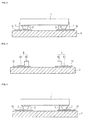
- Fig. 1 is a schematic sectional view illustrating a related-art method of manufacturing an electronic component module.
- a bump 6 is formed on a surface electrode 10 of a substrate 9 by ejecting a metal paste 4 from an ink head 3 and by drying the metal paste 4.
- outer terminals 2 of a bare IC i.e., an electronic component provided with outer terminals
- a bare IC i.e., an electronic component provided with outer terminals
- the bare IC is placed on the substrate 9, and the outer terminals 2 are joined to the bumps 6, respectively, by applying pressure and heat to such an extent that the bumps 6 are deformed.
- the bare IC 1 is thus mounted to the substrate 9.
- Patent Document 1 Japanese Unexamined Patent Application Publication No. 2004-228375
- the related-art manufacturing method described above for example, when the bump 6 is formed in a relatively large thickness, there is a possibility that the deformed bump 6 may extend up to a lateral surface of the bare IC 1, and electrical conduction may occur between the surface electrode 10 of the substrate 9 and an internal wiring of the bare IC 1.
- the electronic component module manufactured by the related-art manufacturing method, described above has a risk that characteristics of the bare IC 1 may degrade.
- Fig. 2 is a sectional view illustrating a structure of the electronic component module manufactured by the related-art manufacturing method.
- a joining portion 7 between the outer terminal 2 of the bare IC 1 and the surface electrode 10 of the substrate 9 is caused to extend up to the lateral surface of the bare IC 1, and the joining portion 7 comes into contact with the lateral surface of the bare IC 1.
- chipping occurs in dicer cutting of the bare IC 1, the internal wiring is often exposed at the lateral surface of the bare IC 1.
- the contact of the joining portion 7 with the lateral surface of the bare IC 1 causes electrical conduction between the surface electrode 10 of the substrate 9 and the internal wiring of the bare IC 1.
- the characteristics of the bare IC 1 degrade.
- the present invention has been accomplished in view of the above-described situation in the art, and an object of the present invention is to provide a method of manufacturing an electronic component module in which joining portions joining a plurality of outer terminals of an electronic component and a plurality of surface electrodes of a substrate are not contacted with a lateral surface of the electronic component, and to provide the electronic component module manufactured by the manufacturing method.
- the present invention provides a method of manufacturing an electronic component module, the method being used to join a plurality of outer terminals of an electronic component respectively to a plurality of bumps provided on one surface of a substrate, the method comprising the steps of forming, on the one surface of the substrate, the plural bumps such that each bump includes a thicker portion having a relatively large thickness and a thinner portion having a relatively small thickness, and that, when looking at the electronic component in a mounted state in a plan view, the thicker portion is positioned on side closer to a center of the electronic component relative to corresponding one of the outer terminals, and the thinner portion is positioned on opposite side away from the center of the electronic component relative to the corresponding outer terminal, and forming a plurality of joining portions, which join the plural outer terminals respectively to the plural bumps, having been formed in the preceding step, through deformation of the bumps, such that a height of each joining portion on the opposite side away from the center of the electronic component when looking at the mounted electronic
- each of the plural bumps includes the thicker portion having a relatively large thickness and the thinner portion having a relatively small thickness.
- Each bump is formed on one surface of the substrate such that, when looking at the electronic component in a mounted state in a plan view, the thicker portion is positioned on the side closer to a center of the electronic component relative to corresponding one of the outer terminals, and the thinner portion is positioned on the opposite side away from the center of the electronic component relative to the corresponding outer terminal.
- the plural joining portions joining the plural outer terminals respectively to the plural bumps, having been formed in the preceding step, through deformation of the bumps are formed such that a height of each joining portion on the opposite side away from the center of the electronic component when looking at the mounted electronic component in a plan view is lower than a height of the joining portion on the side closer to the center of the electronic component. Therefore, the joining portions are avoided from contacting with lateral surfaces of the electronic component. Thus, even when an internal wiring of the electronic component is exposed at the lateral surfaces of the electronic component due to dicer cutting, characteristics of the electronic component do not degrade.
- the plural bumps are each formed in a stepped shape.
- the joining portions can be formed such that the height of each joining portion on the opposite side away from the center of the electronic component when looking at the mounted electronic component in a plan view is lower than the height of the joining portion on the side closer to the center of the electronic component. Therefore, the joining portions are avoided from contacting with the lateral surfaces of the electronic component. Thus, even when the internal wiring of the electronic component is exposed at the lateral surfaces of the electronic component due to dicer cutting, characteristics of the electronic component do not degrade.
- the plural bumps are formed by an ink jet method.
- the thinner portion and the thicker portion having different thicknesses can be easily formed by adjusting the number of times a metal paste is ejected. Furthermore, the thinner portion and the thicker portion can be both formed in a continuous step, and the production cost can be reduced.
- the present invention also provides an electronic component module comprising a substrate, a plurality of bumps provided on one surface of the substrate, an electronic component having a plurality of outer terminals, and a resin sealing surroundings of a plurality of joining portions which join the plural outer terminals respectively to the plural bumps through deformation of the bumps, wherein the plural joining portions are formed such that a height of each joining portion on opposite side away from a center of the electronic component when looking at the electronic component module in a plan view is lower than a height of the joining portion on side closer to the center of the electronic component module.
- the plural joining portions are formed such that the height of each joining portion on the opposite side away from the center of the electronic component when looking at the electronic component in a plan view is lower than the height of the joining portion on the side closer to the center of the electronic component, the joining portions are avoided from contacting with the lateral surfaces of the electronic component.
- the internal wiring of the electronic component is exposed at the lateral surfaces of the electronic component due to dicer cutting, characteristics of the electronic component do not degrade.
- the plural bumps are formed in pairs at opposed positions symmetrical with respect to the center of the electronic component when looking at the electronic component in a plan view.
- the plural bumps are formed in pairs at opposed positions symmetrical with respect to the center of the electronic component when looking at the electronic component in a plan view, a pressing force can be applied in a balanced state and the plural bumps can be deformed evenly when the electronic component is mounted. It is hence possible to avoid bonding strength from being locally changed.
- each of the plural bumps includes the thicker portion having the relatively large thickness and the thinner portion having the relatively small thickness.
- Each bump is formed on one surface of the substrate such that, when looking at the electronic component in a mounted state in a plan view, the thicker portion is positioned on the side closer to the center of the electronic component relative to the corresponding outer terminal, and the thinner portion is positioned on the opposite side away from the center of the electronic component relative to the corresponding outer terminal.
- the plural joining portions joining the plural outer terminals respectively to the plural bumps, having been formed in the preceding step, through deformation of the bumps are formed such that the height of each joining portion on the opposite side away from the center of the electronic component when looking at the mounted electronic component in a plan view is lower than the height of the joining portion on the side closer to the center of the electronic component. Therefore, the joining portions are avoided from contacting with the lateral surfaces of the electronic component. Thus, even when the internal wiring of the electronic component is exposed at the lateral surfaces of the electronic component due to dicer cutting, characteristics of the electronic component do not degrade.
- Fig. 3 is a sectional view illustrating a structure of an electronic component module, in a state before mounting of a bare IC, according to an embodiment of the present invention.
- a surface electrode 10 is provided on one surface of a substrate 9, and a bump 6 is formed in a stepped shape on the surface electrode 10.
- the bump 6 includes a thinner portion 61 having a relatively small thickness, and a thicker portion 62 having a relatively large thickness.
- the thicker portion 62 and the thinner portion 61 are formed on the one surface of the substrate 9 such that, when an electronic component is mounted, the thicker portion 62 is positioned on the side closer to a center of the electronic component relative to a corresponding outer terminal 2 when looking at the mounted electronic component in a plan view, and the thinner portion 61 is positioned on the opposite side away from the center of the electronic component relative to the corresponding outer terminal 2 when looking at the mounted electronic component in a plan view.
- the following description is made in connection with an example in which a bare IC in the form of an electronic component provided with outer terminals is mounted.
- Fig. 4 is a sectional view illustrating a structure of the electronic component module according to the embodiment of the present invention.
- a portion joining the outer terminal 2 and the bump 6 to each other through deformation of the bump 6 is denoted by a joining portion 7.
- the joining portion 7 is formed in a state having a lower height in its region on the opposite side away from the center of the bare IC 1 when looking at the mounted bare IC 1 in a plan view than that in its region on the side closer to the center of the substrate 9 when looking at the mounted bare IC 1 in a plan view. Accordingly, the deformed bump 6 is avoided from extending up to a lateral surface of the bare IC 1.
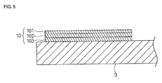
- Fig. 5 is an enlarged sectional view illustrating a part of the substrate 9.
- the substrate 9 is formed of a flexible resin.
- the surface electrode 10 is provided on the one surface of the substrate 9.
- the surface electrode 10 is constituted by forming an Au plating 101 over a nickel layer 102 and a copper layer 103, the latter two serving as ground coatings.
- the bump 6 is formed in a desired shape on the Au plating 101 by ejecting a metal paste from an ink head.
- a metal paste for example, an Ag paste is used as the metal paste.
- the thinner portion 61 and the thicker portion 62 having different thicknesses from each other can be easily formed by adjusting the number of times the metal paste is ejected.
- a method of forming the bump 6 is not limited to the ink jet method.
- the bump 6 may be formed by the screen printing method.
- the thinner portion 61 and the thicker portion 62 can be both formed in a continuous step, and the production cost can be reduced.
- the outer terminal 2 of the bare IC 1 has the shape of an inverted truncated cone and is formed by providing an Au wire bump on an Al pad that is an outer electrode of the bare IC 1.
- the Au wire bump has an outer diameter of 85 ⁇ m and a height of 25 ⁇ m.
- An Au plated bump, a Cu wire bump, or a Cu plated bump may be used instead of the Au wire bump.
- the outer terminal 2 may be formed in a disk-like shape with a plated bump.
- Fig. 6 is a schematic sectional view illustrating a method of manufacturing the electronic component module according to the embodiment of the present invention.
- a metal paste 4 is first ejected from an ink head 3 onto the surface electrode 10 of the substrate 9, thereby forming the thinner portion 61 as illustrated in Fig. 6(b) . More specifically, the metal paste 4 is ejected while a table on which the ink head 3 or the substrate 9 is placed is moved.
- An Ag paste is used as the metal paste 4, and one dot of the Ag paste ejected from the ink head 3 has a volume of 1 pl (1 ⁇ 10 -15 m 3 ).
- the thinner portion 61 having a thickness of 20 ⁇ m is formed by ejecting the metal paste 4 two times while the table on which the ink head 3 is placed is moved in the horizontal direction (right-to-left direction in Fig. 6 ).
- the thicker portion 62 is formed as illustrated in Fig. 6(c) .
- the metal paste 4 is ejected eight times while the table on which the ink head 3 is placed is moved in the horizontal direction.
- the bump 6 is formed with a thickness of 100 ⁇ m in its portion on the side closer to the center of the bare IC 1 when looking at the mounted bare IC 1 in a plan view.
- the formed bump 6 is then dried. Because the ejected metal paste 4 is a minute droplet, the formed bump 6 may be naturally dried without employing a special drying apparatus.
- a ratio of the thickness of the thicker portion 62 and the thickness of the thinner portion 61 is about 5 : 1 in this embodiment, the ratio is not limited to such a value.
- the ratio may be set to 2 : 1 insofar as the deformed bump 6 is avoided from extending up to the lateral surface of the bare IC 1 when the bare IC 1 is mounted.
- the thicker portion 62 has a width of 50 ⁇ m and the thinner portion 61 has a width of 100 ⁇ m in the horizontal direction (right-to-left direction in Fig. 6 ).
- the respective widths of the thicker portion 62 and the thinner portion 61 are not limited to those values, and the width of the thicker portion 62 may be set to 10 ⁇ m, for example.
- the outer terminals 2 of the bare IC (electronic component provided with outer terminals) 1 are aligned to face the bumps 6 on the substrate 9, respectively.
- the bare IC 1 is placed on the substrate 9, and the external terminals 2 are joined to the bumps 6, respectively, by applying pressure and heat to such an extent that the bumps 6 are deformed.
- the bare IC 1 is thus mounted to the substrate 9.
- a center of each outer terminal 2 of the bare IC 1 is positioned to be not overlapped with the thicker portion 62. With such an arrangement, the deformed bump 6 is made less apt to extend up to the lateral surface of the bare IC 1.
- Fig. 7 is a plan seeing-through view illustrating an arrangement of the bumps 6 in the electronic component module according to the embodiment of the present invention.
- the outer terminals 2 of the bare IC 1 are each denoted by a white circle
- the bumps 6 are each denoted by a hatched area.
- the plural bumps 6 are arranged in pairs at opposed positions symmetrical with respect to a center 71 of the bare IC 1 when looking at the bare IC 1 in a plan view.
- the thicker portions 62 of the bumps 6 are also formed in pairs at opposed positions symmetrical with respect to the center 71 of the bare IC 1 when looking at the bare IC 1 in a plan view. Accordingly, when the bare IC 1 is mounted, a pressing force can be applied in a balanced state, and the plural bumps 6 can be deformed in similar ways. It is hence possible to avoid bonding strength from being locally changed.
- the shape of the bump 6 in a plan view is not limited to a rectangle as illustrated in Fig. 7 .
- Fig. 8 is a plan seeing-through view illustrating an arrangement of the bumps 6 in the electronic component module according to the embodiment of the present invention when the bumps 6 have a different shape from that in Fig. 7 .
- the bump 6 may have a substantially elliptic shape in a plan view, by forming the thinner portion 61 having a substantially elliptic shape in a plan view, and the thicker portion 62 having a substantially elliptic shape in a plan view.
- the bumps 6 are formed, similarly to the above-mentioned case, in pairs at opposed positions symmetrical with respect to the center 71 of the bare IC 1 when looking at the bare IC 1 in a plan view. Moreover, the thicker portions 62 of the bumps 6 are also formed in pairs at opposed positions symmetrical with respect to the center 71 of the bare IC 1 when looking at the bare IC 1 in a plan view.
- Fig. 9 is a plan seeing-through view illustrating an arrangement of the bumps 6 in the electronic component module according to the embodiment of the present invention when the bare IC 1 has two outer terminals 2.
- the outer terminals 2 are each formed in a rectangular shape, when viewed in a plan view, in many cases from the viewpoint of mounting the bare IC 1 in a stable state.
- a similar advantageous effect to that described above is expected by forming the bump 6 in such a stepped shape that the thicker portion 62 is positioned on the side closer to the center of the bare IC 1 when looking at the bare IC 1 in a plan view than a center line of the outer terminal 2 extending in the lengthwise direction thereof, and that the thinner portion 61 is positioned on the opposite side with respect to the center line of the outer terminal 2.
- the plural joining portions 7 joining the plural outer terminals 2 respectively to the plural bumps 6, having been formed in the preceding step, through deformation of the bumps 6 are each formed such that the height of the joining portion 7 on the opposite side away from the center of the bare IC 1 when looking at the bare IC 1 in a plan view is lower than the height of the joining portion 7 on the side closer to the center of the bare IC 1 when looking at the bare IC 1 in a plan view. Therefore, the joining portion 7 is avoided from contacting with the lateral surface of the bare IC 1. Thus, even when the internal wiring of the bare IC 1 is exposed at the lateral surface of the bare IC 1 due to dicer cutting, characteristics of the bare IC 1 do not degrade.
- Fig. 10 is a sectional view illustrating a structure of the electronic component module, in a state before mounting of the bare IC 1, according to the embodiment of the present invention when the bumps 6 have other different shapes.
- Fig. 10(a) illustrates an example in which the bump 6 is formed in a three-step shape including a thicker portion, an intermediate portion, and a thinner portion.
- the bump 6 is formed such that those three portions have thicknesses gradually increasing toward the side closer to the center of the bare IC 1 when looking at the mounted bare IC 1 in a plan view.
- the bump 6 may be formed in a sloped shape having a thickness that gradually increases toward the side closer to the center of the bare IC 1 when looking at the mounted bare IC 1 in a plan view, as illustrated in Fig. 10(b) .
- the present invention is not limited to the above-described embodiment, and it may be variously modified and improved without departing from the scope of the present invention.
- applications of the present invention are not limited to an electronic component module in which an electronic component, e.g., a bare IC, is mounted to a substrate
- the present invention is also applicable to an electronic component module in which a medium-sized electronic component incorporating a small-sized electronic component therein is mounted to a substrate.
- the present invention can be applied to an electronic component module in which, after resin-molding a small-sized electronic component together with a substrate, an electromagnetic shield portion is formed on a top surface or a lateral surface of the electronic component module.
Landscapes
- Engineering & Computer Science (AREA)
- Microelectronics & Electronic Packaging (AREA)
- Manufacturing & Machinery (AREA)
- Wire Bonding (AREA)
- Encapsulation Of And Coatings For Semiconductor Or Solid State Devices (AREA)
- Physics & Mathematics (AREA)
- Geometry (AREA)
- Non-Metallic Protective Coatings For Printed Circuits (AREA)
Abstract
Description
- The present invention relates to a method of manufacturing an electronic component module, the method being used to respectively join a plurality of outer terminals of an electronic component to a plurality of bumps provided on one surface of a substrate, and also relates to the electronic component module manufactured by the manufacturing method.
-
Patent Document 1 discloses a method of forming bumps when a semiconductor is joined to a substrate with the bumps interposed between them.Fig. 1 is a schematic sectional view illustrating a related-art method of manufacturing an electronic component module. InPatent Document 1, as illustrated inFig. 1(a) , abump 6 is formed on asurface electrode 10 of asubstrate 9 by ejecting ametal paste 4 from anink head 3 and by drying themetal paste 4. - Next, as illustrated in
Fig. 1(b) ,outer terminals 2 of a bare IC (i.e., an electronic component provided with outer terminals) 1 are aligned to face thebumps 6 on thesubstrate 9, respectively. Furthermore, as illustrated inFig. 1(c) , the bare IC is placed on thesubstrate 9, and theouter terminals 2 are joined to thebumps 6, respectively, by applying pressure and heat to such an extent that thebumps 6 are deformed. Thebare IC 1 is thus mounted to thesubstrate 9. - Patent Document 1: Japanese Unexamined Patent Application Publication No.
2004-228375 - With the related-art manufacturing method described above, for example, when the
bump 6 is formed in a relatively large thickness, there is a possibility that thedeformed bump 6 may extend up to a lateral surface of thebare IC 1, and electrical conduction may occur between thesurface electrode 10 of thesubstrate 9 and an internal wiring of thebare IC 1. Thus, the electronic component module manufactured by the related-art manufacturing method, described above, has a risk that characteristics of thebare IC 1 may degrade. -
Fig. 2 is a sectional view illustrating a structure of the electronic component module manufactured by the related-art manufacturing method. When thebump 6 is formed in a relatively large thickness, a joiningportion 7 between theouter terminal 2 of thebare IC 1 and thesurface electrode 10 of thesubstrate 9 is caused to extend up to the lateral surface of thebare IC 1, and the joiningportion 7 comes into contact with the lateral surface of thebare IC 1. If chipping occurs in dicer cutting of thebare IC 1, the internal wiring is often exposed at the lateral surface of thebare IC 1. In such a case, the contact of the joiningportion 7 with the lateral surface of thebare IC 1 causes electrical conduction between thesurface electrode 10 of thesubstrate 9 and the internal wiring of thebare IC 1. As a result, the characteristics of thebare IC 1 degrade. - The present invention has been accomplished in view of the above-described situation in the art, and an object of the present invention is to provide a method of manufacturing an electronic component module in which joining portions joining a plurality of outer terminals of an electronic component and a plurality of surface electrodes of a substrate are not contacted with a lateral surface of the electronic component, and to provide the electronic component module manufactured by the manufacturing method.
- To achieve the above-mentioned object, the present invention provides a method of manufacturing an electronic component module, the method being used to join a plurality of outer terminals of an electronic component respectively to a plurality of bumps provided on one surface of a substrate, the method comprising the steps of forming, on the one surface of the substrate, the plural bumps such that each bump includes a thicker portion having a relatively large thickness and a thinner portion having a relatively small thickness, and that, when looking at the electronic component in a mounted state in a plan view, the thicker portion is positioned on side closer to a center of the electronic component relative to corresponding one of the outer terminals, and the thinner portion is positioned on opposite side away from the center of the electronic component relative to the corresponding outer terminal, and forming a plurality of joining portions, which join the plural outer terminals respectively to the plural bumps, having been formed in the preceding step, through deformation of the bumps, such that a height of each joining portion on the opposite side away from the center of the electronic component when looking at the mounted electronic component in a plan view is lower than a height of the joining portion on the side closer to the center of the electronic component.
- With the feature mentioned above, each of the plural bumps includes the thicker portion having a relatively large thickness and the thinner portion having a relatively small thickness. Each bump is formed on one surface of the substrate such that, when looking at the electronic component in a mounted state in a plan view, the thicker portion is positioned on the side closer to a center of the electronic component relative to corresponding one of the outer terminals, and the thinner portion is positioned on the opposite side away from the center of the electronic component relative to the corresponding outer terminal. The plural joining portions joining the plural outer terminals respectively to the plural bumps, having been formed in the preceding step, through deformation of the bumps are formed such that a height of each joining portion on the opposite side away from the center of the electronic component when looking at the mounted electronic component in a plan view is lower than a height of the joining portion on the side closer to the center of the electronic component. Therefore, the joining portions are avoided from contacting with lateral surfaces of the electronic component. Thus, even when an internal wiring of the electronic component is exposed at the lateral surfaces of the electronic component due to dicer cutting, characteristics of the electronic component do not degrade.
- In the method of manufacturing the electronic component module according to the present invention, preferably, the plural bumps are each formed in a stepped shape.
- With the feature mentioned above, since the plural bumps are each formed in a stepped shape, the joining portions can be formed such that the height of each joining portion on the opposite side away from the center of the electronic component when looking at the mounted electronic component in a plan view is lower than the height of the joining portion on the side closer to the center of the electronic component. Therefore, the joining portions are avoided from contacting with the lateral surfaces of the electronic component. Thus, even when the internal wiring of the electronic component is exposed at the lateral surfaces of the electronic component due to dicer cutting, characteristics of the electronic component do not degrade.
- In the method of manufacturing the electronic component module according to the present invention, preferably, the plural bumps are formed by an ink jet method.
- With the feature mentioned above, since the plural bumps are formed by an ink jet method, the thinner portion and the thicker portion having different thicknesses can be easily formed by adjusting the number of times a metal paste is ejected. Furthermore, the thinner portion and the thicker portion can be both formed in a continuous step, and the production cost can be reduced.
- To achieve the above-mentioned object, the present invention also provides an electronic component module comprising a substrate, a plurality of bumps provided on one surface of the substrate, an electronic component having a plurality of outer terminals, and a resin sealing surroundings of a plurality of joining portions which join the plural outer terminals respectively to the plural bumps through deformation of the bumps, wherein the plural joining portions are formed such that a height of each joining portion on opposite side away from a center of the electronic component when looking at the electronic component module in a plan view is lower than a height of the joining portion on side closer to the center of the electronic component module.
- With the feature mentioned above, since the plural joining portions are formed such that the height of each joining portion on the opposite side away from the center of the electronic component when looking at the electronic component in a plan view is lower than the height of the joining portion on the side closer to the center of the electronic component, the joining portions are avoided from contacting with the lateral surfaces of the electronic component. Thus, even when the internal wiring of the electronic component is exposed at the lateral surfaces of the electronic component due to dicer cutting, characteristics of the electronic component do not degrade.
- In the electronic component module according to the present invention, preferably, the plural bumps are formed in pairs at opposed positions symmetrical with respect to the center of the electronic component when looking at the electronic component in a plan view.
- With the feature mentioned above, since the plural bumps are formed in pairs at opposed positions symmetrical with respect to the center of the electronic component when looking at the electronic component in a plan view, a pressing force can be applied in a balanced state and the plural bumps can be deformed evenly when the electronic component is mounted. It is hence possible to avoid bonding strength from being locally changed.
- With the features described above, each of the plural bumps includes the thicker portion having the relatively large thickness and the thinner portion having the relatively small thickness. Each bump is formed on one surface of the substrate such that, when looking at the electronic component in a mounted state in a plan view, the thicker portion is positioned on the side closer to the center of the electronic component relative to the corresponding outer terminal, and the thinner portion is positioned on the opposite side away from the center of the electronic component relative to the corresponding outer terminal. The plural joining portions joining the plural outer terminals respectively to the plural bumps, having been formed in the preceding step, through deformation of the bumps are formed such that the height of each joining portion on the opposite side away from the center of the electronic component when looking at the mounted electronic component in a plan view is lower than the height of the joining portion on the side closer to the center of the electronic component. Therefore, the joining portions are avoided from contacting with the lateral surfaces of the electronic component. Thus, even when the internal wiring of the electronic component is exposed at the lateral surfaces of the electronic component due to dicer cutting, characteristics of the electronic component do not degrade.
-
- [
Fig. 1] Fig. 1 is a schematic sectional view illustrating a related-art method of manufacturing an electronic component module. - [
Fig. 2] Fig. 2 is a sectional view illustrating a structure of the electronic component module manufactured by the related-art manufacturing method. - [
Fig. 3] Fig. 3 is a sectional view illustrating a structure of an electronic component module, in a state before mounting of a bare IC, according to an embodiment of the present invention. - [
Fig. 4] Fig. 4 is a sectional view illustrating a structure of the electronic component module according to the embodiment of the present invention. - [
Fig. 5] Fig. 5 is an enlarged sectional view illustrating a part of a substrate. - [
Fig. 6] Fig. 6 is a schematic sectional view illustrating a method of manufacturing the electronic component module according to the embodiment of the present invention. - [
Fig. 7] Fig. 7 is a plan seeing-through view illustrating an arrangement of bumps in the electronic component module according to the embodiment of the present invention. - [
Fig. 8] Fig. 8 is a plan seeing-through view illustrating an arrangement of bumps in the electronic component module according to the embodiment of the present invention when the bumps have a different shape from that inFig. 7 . - [
Fig. 9] Fig. 9 is a plan seeing-through view illustrating an arrangement of bumps in the electronic component module according to the embodiment of the present invention when the bare IC has two outer terminals. - [
Fig. 10] Fig. 10 is a sectional view illustrating a structure of the electronic component module, in a state before mounting of the bare IC, according to the embodiment of the present invention when the bumps have other different shapes. - An embodiment of the present invention will be described in detail below with reference to the drawings.
-
Fig. 3 is a sectional view illustrating a structure of an electronic component module, in a state before mounting of a bare IC, according to an embodiment of the present invention. As illustrated inFig. 3 , asurface electrode 10 is provided on one surface of asubstrate 9, and abump 6 is formed in a stepped shape on thesurface electrode 10. - In more detail, the
bump 6 includes athinner portion 61 having a relatively small thickness, and athicker portion 62 having a relatively large thickness. Thethicker portion 62 and thethinner portion 61 are formed on the one surface of thesubstrate 9 such that, when an electronic component is mounted, thethicker portion 62 is positioned on the side closer to a center of the electronic component relative to a correspondingouter terminal 2 when looking at the mounted electronic component in a plan view, and thethinner portion 61 is positioned on the opposite side away from the center of the electronic component relative to the correspondingouter terminal 2 when looking at the mounted electronic component in a plan view. The following description is made in connection with an example in which a bare IC in the form of an electronic component provided with outer terminals is mounted. -
Fig. 4 is a sectional view illustrating a structure of the electronic component module according to the embodiment of the present invention. After aligning theouter terminals 2 of abare IC 1 to face thebumps 6 on thesubstrate 9, respectively, thebare IC 1 is placed on thesubstrate 9, and theouter terminals 2 are joined to thebumps 6, respectively, by applying pressure and heat to such an extent that thebumps 6 are deformed, as illustrated inFig. 4 . Thebare IC 1 is thus mounted to thesubstrate 9. - In this embodiment, a portion joining the
outer terminal 2 and thebump 6 to each other through deformation of thebump 6 is denoted by a joiningportion 7. The joiningportion 7 is formed in a state having a lower height in its region on the opposite side away from the center of thebare IC 1 when looking at the mountedbare IC 1 in a plan view than that in its region on the side closer to the center of thesubstrate 9 when looking at the mountedbare IC 1 in a plan view. Accordingly, thedeformed bump 6 is avoided from extending up to a lateral surface of thebare IC 1. As a result, even when chipping occurs in dicer cutting of thebare IC 1 and an internal wiring of thebare IC 1 is exposed at the lateral surface of thebare IC 1, electrical conduction between thesurface electrode 10 of thesubstrate 9 and the internal wiring of thebare IC 1 is not caused. Hence characteristics of thebare IC 1 do not degrade. - A method of manufacturing the electronic component module according to this embodiment will be described in detail below.
Fig. 5 is an enlarged sectional view illustrating a part of thesubstrate 9. Thesubstrate 9 is formed of a flexible resin. As illustrated inFig. 5 , thesurface electrode 10 is provided on the one surface of thesubstrate 9. Thesurface electrode 10 is constituted by forming an Au plating 101 over anickel layer 102 and acopper layer 103, the latter two serving as ground coatings. - The
bump 6 is formed in a desired shape on the Au plating 101 by ejecting a metal paste from an ink head. For example, an Ag paste is used as the metal paste. Thethinner portion 61 and thethicker portion 62 having different thicknesses from each other can be easily formed by adjusting the number of times the metal paste is ejected. - Of course, a method of forming the
bump 6 is not limited to the ink jet method. As another example, thebump 6 may be formed by the screen printing method. When thebump 6 is formed by the screen printing method, it is required to, after forming thethinner portion 61, dry the printedthinner portion 61 and then form thethicker portion 62 on a part of thethinner portion 61 after replacing a screen plate. On the other hand, when thebump 6 is formed by the ink jet method, thethinner portion 61 and thethicker portion 62 can be both formed in a continuous step, and the production cost can be reduced. - The
outer terminal 2 of thebare IC 1 has the shape of an inverted truncated cone and is formed by providing an Au wire bump on an Al pad that is an outer electrode of thebare IC 1. In this embodiment, the Au wire bump has an outer diameter of 85 µm and a height of 25 µm. An Au plated bump, a Cu wire bump, or a Cu plated bump may be used instead of the Au wire bump. Furthermore, theouter terminal 2 may be formed in a disk-like shape with a plated bump. -
Fig. 6 is a schematic sectional view illustrating a method of manufacturing the electronic component module according to the embodiment of the present invention. As illustrated inFig. 6(a) , ametal paste 4 is first ejected from anink head 3 onto thesurface electrode 10 of thesubstrate 9, thereby forming thethinner portion 61 as illustrated inFig. 6(b) . More specifically, themetal paste 4 is ejected while a table on which theink head 3 or thesubstrate 9 is placed is moved. An Ag paste is used as themetal paste 4, and one dot of the Ag paste ejected from theink head 3 has a volume of 1 pl (1 × 10-15 m3). In this embodiment, thethinner portion 61 having a thickness of 20 µm is formed by ejecting themetal paste 4 two times while the table on which theink head 3 is placed is moved in the horizontal direction (right-to-left direction inFig. 6 ). - Next, the
thicker portion 62 is formed as illustrated inFig. 6(c) . When forming thethicker portion 62, themetal paste 4 is ejected eight times while the table on which theink head 3 is placed is moved in the horizontal direction. As a result, thebump 6 is formed with a thickness of 100 µm in its portion on the side closer to the center of thebare IC 1 when looking at the mountedbare IC 1 in a plan view. The formedbump 6 is then dried. Because the ejectedmetal paste 4 is a minute droplet, the formedbump 6 may be naturally dried without employing a special drying apparatus. - While a ratio of the thickness of the
thicker portion 62 and the thickness of thethinner portion 61 is about 5 : 1 in this embodiment, the ratio is not limited to such a value. For example, the ratio may be set to 2 : 1 insofar as thedeformed bump 6 is avoided from extending up to the lateral surface of thebare IC 1 when thebare IC 1 is mounted. Furthermore, in this embodiment, thethicker portion 62 has a width of 50 µm and thethinner portion 61 has a width of 100 µm in the horizontal direction (right-to-left direction inFig. 6 ). However, the respective widths of thethicker portion 62 and thethinner portion 61 are not limited to those values, and the width of thethicker portion 62 may be set to 10 µm, for example. - After drying the formed
bumps 6, theouter terminals 2 of the bare IC (electronic component provided with outer terminals) 1 are aligned to face thebumps 6 on thesubstrate 9, respectively. Next, as illustrated inFig. 6(d) , thebare IC 1 is placed on thesubstrate 9, and theexternal terminals 2 are joined to thebumps 6, respectively, by applying pressure and heat to such an extent that thebumps 6 are deformed. Thebare IC 1 is thus mounted to thesubstrate 9. In the above-mentioned alignment of theouter terminals 2, a center of eachouter terminal 2 of thebare IC 1 is positioned to be not overlapped with thethicker portion 62. With such an arrangement, thedeformed bump 6 is made less apt to extend up to the lateral surface of thebare IC 1. -
Fig. 7 is a plan seeing-through view illustrating an arrangement of thebumps 6 in the electronic component module according to the embodiment of the present invention. InFig. 7 , theouter terminals 2 of thebare IC 1 are each denoted by a white circle, and thebumps 6 are each denoted by a hatched area. Theplural bumps 6 are arranged in pairs at opposed positions symmetrical with respect to acenter 71 of thebare IC 1 when looking at thebare IC 1 in a plan view. - The
thicker portions 62 of thebumps 6 are also formed in pairs at opposed positions symmetrical with respect to thecenter 71 of thebare IC 1 when looking at thebare IC 1 in a plan view. Accordingly, when thebare IC 1 is mounted, a pressing force can be applied in a balanced state, and theplural bumps 6 can be deformed in similar ways. It is hence possible to avoid bonding strength from being locally changed. - The shape of the
bump 6 in a plan view is not limited to a rectangle as illustrated inFig. 7 .Fig. 8 is a plan seeing-through view illustrating an arrangement of thebumps 6 in the electronic component module according to the embodiment of the present invention when thebumps 6 have a different shape from that inFig. 7 . As illustrated inFig. 8 , thebump 6 may have a substantially elliptic shape in a plan view, by forming thethinner portion 61 having a substantially elliptic shape in a plan view, and thethicker portion 62 having a substantially elliptic shape in a plan view. In such a case, thebumps 6 are formed, similarly to the above-mentioned case, in pairs at opposed positions symmetrical with respect to thecenter 71 of thebare IC 1 when looking at thebare IC 1 in a plan view. Moreover, thethicker portions 62 of thebumps 6 are also formed in pairs at opposed positions symmetrical with respect to thecenter 71 of thebare IC 1 when looking at thebare IC 1 in a plan view. - The number of the
outer terminals 2 is not limited to particular one, and the least necessary number of theouter terminals 2 is two.Fig. 9 is a plan seeing-through view illustrating an arrangement of thebumps 6 in the electronic component module according to the embodiment of the present invention when thebare IC 1 has twoouter terminals 2. - As illustrated in
Fig. 9 , when the number of theouter terminals 2 is two, theouter terminals 2 are each formed in a rectangular shape, when viewed in a plan view, in many cases from the viewpoint of mounting thebare IC 1 in a stable state. A similar advantageous effect to that described above is expected by forming thebump 6 in such a stepped shape that thethicker portion 62 is positioned on the side closer to the center of thebare IC 1 when looking at thebare IC 1 in a plan view than a center line of theouter terminal 2 extending in the lengthwise direction thereof, and that thethinner portion 61 is positioned on the opposite side with respect to the center line of theouter terminal 2. - Returning to
Fig. 6 , the surroundings of the joiningportion 7 are finally sealed by an insulatingresin 8 as illustrated inFig. 6(e) , whereby the electronic component module is completed. - According to this embodiment, as described above, the
plural joining portions 7 joining the pluralouter terminals 2 respectively to theplural bumps 6, having been formed in the preceding step, through deformation of thebumps 6 are each formed such that the height of the joiningportion 7 on the opposite side away from the center of thebare IC 1 when looking at thebare IC 1 in a plan view is lower than the height of the joiningportion 7 on the side closer to the center of thebare IC 1 when looking at thebare IC 1 in a plan view. Therefore, the joiningportion 7 is avoided from contacting with the lateral surface of thebare IC 1. Thus, even when the internal wiring of thebare IC 1 is exposed at the lateral surface of thebare IC 1 due to dicer cutting, characteristics of thebare IC 1 do not degrade. - While, in the embodiment described above, the
bump 6 is formed in a two-step shape including thethicker portion 62 and thethinner portion 61, the shape of thebump 6 is not particularly limited to the two-step shape.Fig. 10 is a sectional view illustrating a structure of the electronic component module, in a state before mounting of thebare IC 1, according to the embodiment of the present invention when thebumps 6 have other different shapes. -
Fig. 10(a) illustrates an example in which thebump 6 is formed in a three-step shape including a thicker portion, an intermediate portion, and a thinner portion. As a matter of course, thebump 6 is formed such that those three portions have thicknesses gradually increasing toward the side closer to the center of thebare IC 1 when looking at the mountedbare IC 1 in a plan view. Alternatively, when an amount of themetal paste 4 ejected from theink head 3 can be finely controlled, thebump 6 may be formed in a sloped shape having a thickness that gradually increases toward the side closer to the center of thebare IC 1 when looking at the mountedbare IC 1 in a plan view, as illustrated inFig. 10(b) . - The present invention is not limited to the above-described embodiment, and it may be variously modified and improved without departing from the scope of the present invention. For example, applications of the present invention are not limited to an electronic component module in which an electronic component, e.g., a bare IC, is mounted to a substrate, and the present invention is also applicable to an electronic component module in which a medium-sized electronic component incorporating a small-sized electronic component therein is mounted to a substrate. As one example, the present invention can be applied to an electronic component module in which, after resin-molding a small-sized electronic component together with a substrate, an electromagnetic shield portion is formed on a top surface or a lateral surface of the electronic component module.
-
- 1
- bare IC (electronic component provided with outer terminals)
- 2
- outer terminal
- 4
- metal paste
- 6
- bump
- 7
- joining portion
- 8
- insulating resin
- 9
- substrate
- 10
- surface electrode
- 61
- thinner portion
- 62
- thicker portion
Claims (5)
- A method of manufacturing an electronic component module, the method being used to join a plurality of outer terminals of an electronic component respectively to a plurality of bumps provided on one surface of a substrate, the method comprising the steps of:forming, on the one surface of the substrate, the plural bumps such that each bump includes a thicker portion having a relatively large thickness and a thinner portion having a relatively small thickness, and that, when looking at the electronic component in a mounted state in a plan view, the thicker portion is positioned on side closer to a center of the electronic component relative to corresponding one of the outer terminals, and the thinner portion is positioned on opposite side away from the center of the electronic component relative to the corresponding outer terminal; andforming a plurality of joining portions, which join the plural outer terminals respectively to the plural bumps, having been formed in the preceding step, through deformation of the bumps, such that a height of each joining portion on the opposite side away from the center of the electronic component when looking at the mounted electronic component in a plan view is lower than a height of the joining portion on the side closer to the center of the electronic component.
- The method of manufacturing the electronic component module according to Claim 1, wherein the plural bumps are each formed in a stepped shape.
- The method of manufacturing the electronic component module according to Claim 1 or 2, wherein the plural bumps are formed by an ink jet method.
- An electronic component module comprising:a substrate;a plurality of bumps provided on one surface of the substrate;an electronic component having a plurality of outer terminals; anda resin sealing surroundings of a plurality of joining portions which join the plural outer terminals respectively to the plural bumps through deformation of the bumps,wherein the plural joining portions are formed such that a height of each joining portion on opposite side away from a center of the electronic component when looking at the electronic component module in a plan view is lower than a height of the joining portion on side closer to the center of the electronic component module.
- The electronic component module according to Claim 4, wherein the plural bumps are formed in pairs at opposed positions symmetrical with respect to the center of the electronic component when looking at the electronic component in a plan view.
Applications Claiming Priority (2)
| Application Number | Priority Date | Filing Date | Title |
|---|---|---|---|
| JP2011099951 | 2011-04-27 | ||
| PCT/JP2012/059305 WO2012147480A1 (en) | 2011-04-27 | 2012-04-05 | Method for producing electronic component module and electronic component module |
Publications (2)
| Publication Number | Publication Date |
|---|---|
| EP2704185A1 true EP2704185A1 (en) | 2014-03-05 |
| EP2704185A4 EP2704185A4 (en) | 2014-10-29 |
Family
ID=47072004
Family Applications (1)
| Application Number | Title | Priority Date | Filing Date |
|---|---|---|---|
| EP12775989.2A Withdrawn EP2704185A4 (en) | 2011-04-27 | 2012-04-05 | METHOD FOR MANUFACTURING ELECTRONIC COMPONENT MODULE AND ELECTRONIC COMPONENT MODULE |
Country Status (6)
| Country | Link |
|---|---|
| US (2) | US9532495B2 (en) |
| EP (1) | EP2704185A4 (en) |
| JP (1) | JP5626460B2 (en) |
| KR (1) | KR101489146B1 (en) |
| CN (1) | CN103493191B (en) |
| WO (1) | WO2012147480A1 (en) |
Cited By (1)
| Publication number | Priority date | Publication date | Assignee | Title |
|---|---|---|---|---|
| EP3668284A1 (en) * | 2018-12-13 | 2020-06-17 | Endress+Hauser SE+Co. KG | Circuit board and method for manufacturing a circuit board |
Families Citing this family (1)
| Publication number | Priority date | Publication date | Assignee | Title |
|---|---|---|---|---|
| US10600755B2 (en) * | 2017-08-10 | 2020-03-24 | Amkor Technology, Inc. | Method of manufacturing an electronic device and electronic device manufactured thereby |
Family Cites Families (21)
| Publication number | Priority date | Publication date | Assignee | Title |
|---|---|---|---|---|
| DE3824865A1 (en) * | 1988-07-21 | 1990-01-25 | Productech Gmbh | MANUFACTURE OF SOLAR AREAS |
| US5291375A (en) * | 1991-09-30 | 1994-03-01 | Kabushiki Kaisha Toshiba | Printed circuit board and electric device configured to facilitate bonding |
| JPH0677632A (en) * | 1992-02-24 | 1994-03-18 | Matsushita Electric Ind Co Ltd | Circuit board |
| US5400950A (en) * | 1994-02-22 | 1995-03-28 | Delco Electronics Corporation | Method for controlling solder bump height for flip chip integrated circuit devices |
| US5663529A (en) * | 1995-09-14 | 1997-09-02 | Ford Motor Company | Anti-skew mounting pads and processing method for electronic surface mount components |
| JP3783754B2 (en) * | 1998-02-27 | 2006-06-07 | 富士ゼロックス株式会社 | Insulating substrate, semiconductor device, and semiconductor mounting device |
| JP3420076B2 (en) * | 1998-08-31 | 2003-06-23 | 新光電気工業株式会社 | Method for manufacturing flip-chip mounting board, flip-chip mounting board, and flip-chip mounting structure |
| JP2001284783A (en) * | 2000-03-30 | 2001-10-12 | Shinko Electric Ind Co Ltd | Surface mounting substrate and surface mounting structure |
| JP2004228375A (en) | 2003-01-23 | 2004-08-12 | Seiko Epson Corp | Bump formation method, device, and electronic apparatus |
| JP4175197B2 (en) * | 2003-06-27 | 2008-11-05 | 株式会社デンソー | Flip chip mounting structure |
| US7860495B2 (en) * | 2004-08-09 | 2010-12-28 | Siemens Industry Inc. | Wireless building control architecture |
| EP1720389B1 (en) * | 2005-04-25 | 2019-07-03 | Brother Kogyo Kabushiki Kaisha | Method for forming pattern and a wired board |
| JP4817892B2 (en) * | 2005-06-28 | 2011-11-16 | 富士通セミコンダクター株式会社 | Semiconductor device |
| JP2008060438A (en) | 2006-09-01 | 2008-03-13 | Matsushita Electric Ind Co Ltd | Electronic component mounting apparatus and electronic component mounting method |
| JP2008060483A (en) * | 2006-09-01 | 2008-03-13 | Sharp Corp | Semiconductor device mounting structure and method of manufacturing the same |
| JP4962217B2 (en) * | 2007-08-28 | 2012-06-27 | 富士通株式会社 | Printed wiring board and electronic device manufacturing method |
| US7851928B2 (en) * | 2008-06-10 | 2010-12-14 | Texas Instruments Incorporated | Semiconductor device having substrate with differentially plated copper and selective solder |
| US9095066B2 (en) * | 2008-06-18 | 2015-07-28 | Semiconductor Energy Laboratory Co., Ltd. | Printed board |
| US8018027B2 (en) * | 2009-10-30 | 2011-09-13 | Murata Manufacturing Co., Ltd. | Flip-bonded dual-substrate inductor, flip-bonded dual-substrate inductor, and integrated passive device including a flip-bonded dual-substrate inductor |
| JP5991915B2 (en) * | 2012-12-27 | 2016-09-14 | ルネサスエレクトロニクス株式会社 | Manufacturing method of semiconductor device |
| JP6476871B2 (en) * | 2014-05-22 | 2019-03-06 | 株式会社村田製作所 | Circuit board, power storage device, battery pack and electronic device |
-
2012
- 2012-04-05 JP JP2013511987A patent/JP5626460B2/en active Active
- 2012-04-05 EP EP12775989.2A patent/EP2704185A4/en not_active Withdrawn
- 2012-04-05 WO PCT/JP2012/059305 patent/WO2012147480A1/en not_active Ceased
- 2012-04-05 CN CN201280020504.9A patent/CN103493191B/en active Active
- 2012-04-05 KR KR1020137027639A patent/KR101489146B1/en active Active
-
2013
- 2013-10-24 US US14/062,767 patent/US9532495B2/en active Active
-
2016
- 2016-11-16 US US15/353,362 patent/US10177108B2/en active Active
Cited By (1)
| Publication number | Priority date | Publication date | Assignee | Title |
|---|---|---|---|---|
| EP3668284A1 (en) * | 2018-12-13 | 2020-06-17 | Endress+Hauser SE+Co. KG | Circuit board and method for manufacturing a circuit board |
Also Published As
| Publication number | Publication date |
|---|---|
| CN103493191B (en) | 2017-09-26 |
| KR20130136545A (en) | 2013-12-12 |
| US20170084566A1 (en) | 2017-03-23 |
| JPWO2012147480A1 (en) | 2014-07-28 |
| EP2704185A4 (en) | 2014-10-29 |
| US20140049922A1 (en) | 2014-02-20 |
| US9532495B2 (en) | 2016-12-27 |
| CN103493191A (en) | 2014-01-01 |
| US10177108B2 (en) | 2019-01-08 |
| JP5626460B2 (en) | 2014-11-19 |
| WO2012147480A1 (en) | 2012-11-01 |
| KR101489146B1 (en) | 2015-02-03 |
Similar Documents
| Publication | Publication Date | Title |
|---|---|---|
| KR100523495B1 (en) | Semiconductor device and fabrication method thereof | |
| CN100561737C (en) | Stacked ball grid array package of center-bonded chip and manufacturing method thereof | |
| KR100288035B1 (en) | Flip chip connection method, flip chip connection structure and electronic device using same | |
| KR20080080406A (en) | Microelectronic Assemblies with Ultrafine Pitch Stacks | |
| US20090102049A1 (en) | Semiconductor device, layered type semiconductor device using the same, base substrate and semiconductor device manufacturing method | |
| US20130133193A1 (en) | Surface mount technology process for advanced quad flat no-lead package process and stencil used therewith | |
| US10177108B2 (en) | Method of manufacturing electronic component module and electronic component module | |
| US10219380B2 (en) | Electronic device module and manufacturing method thereof | |
| TW471077B (en) | Bump forming method, bump forming bonding tool, semiconductor wafer, semiconductor chip, semiconductor device, manufacture thereof, circuit board and electronic machine | |
| US12610837B2 (en) | Laterally mounted and packaged structure and manufacturing method thereof | |
| US8077466B2 (en) | Heat sink, semiconductor device, and method of manufacturing heat sink | |
| JP6268791B2 (en) | Resin multilayer substrate and manufacturing method thereof | |
| JP2013229358A (en) | Semiconductor device and method of manufacturing the same | |
| JP5818654B2 (en) | Multi-cavity wiring board, wiring board and electronic device | |
| JP3777131B2 (en) | Electronic component mounting method | |
| JP4699089B2 (en) | Chip-on-film semiconductor device | |
| JP4954778B2 (en) | Three-dimensional electronic circuit device and connecting member | |
| KR100891652B1 (en) | Semiconductor chip mounting board | |
| US20050003576A1 (en) | Semiconductor device manufacturing method | |
| JP2010010586A (en) | Flip-connection package and method of manufacturing flip-connection package | |
| JP4045718B2 (en) | Resin-sealed semiconductor device and manufacturing method thereof | |
| US20170367195A1 (en) | Printed circuit board and manufacturing method thereof | |
| JP2006135357A (en) | Multiple wiring board | |
| JP2002190552A (en) | Method for manufacturing semiconductor device | |
| JP2008283088A (en) | Manufacturing method of semiconductor module and semiconductor module |
Legal Events
| Date | Code | Title | Description |
|---|---|---|---|
| PUAI | Public reference made under article 153(3) epc to a published international application that has entered the european phase |
Free format text: ORIGINAL CODE: 0009012 |
|
| 17P | Request for examination filed |
Effective date: 20131122 |
|
| AK | Designated contracting states |
Kind code of ref document: A1 Designated state(s): AL AT BE BG CH CY CZ DE DK EE ES FI FR GB GR HR HU IE IS IT LI LT LU LV MC MK MT NL NO PL PT RO RS SE SI SK SM TR |
|
| DAX | Request for extension of the european patent (deleted) | ||
| A4 | Supplementary search report drawn up and despatched |
Effective date: 20140930 |
|
| RIC1 | Information provided on ipc code assigned before grant |
Ipc: H01L 23/12 20060101ALI20140924BHEP Ipc: H01L 23/498 20060101ALI20140924BHEP Ipc: H01L 21/60 20060101AFI20140924BHEP |
|
| STAA | Information on the status of an ep patent application or granted ep patent |
Free format text: STATUS: EXAMINATION IS IN PROGRESS |
|
| 17Q | First examination report despatched |
Effective date: 20180627 |
|
| GRAP | Despatch of communication of intention to grant a patent |
Free format text: ORIGINAL CODE: EPIDOSNIGR1 |
|
| STAA | Information on the status of an ep patent application or granted ep patent |
Free format text: STATUS: GRANT OF PATENT IS INTENDED |
|
| RIC1 | Information provided on ipc code assigned before grant |
Ipc: H01L 23/498 20060101ALI20200630BHEP Ipc: H01L 23/485 20060101ALI20200630BHEP Ipc: H05K 3/34 20060101ALI20200630BHEP Ipc: H01L 21/60 20060101AFI20200630BHEP |
|
| INTG | Intention to grant announced |
Effective date: 20200716 |
|
| RIN1 | Information on inventor provided before grant (corrected) |
Inventor name: KIYONO, SHINYA Inventor name: SATAKE, YOSHIAKI |
|
| STAA | Information on the status of an ep patent application or granted ep patent |
Free format text: STATUS: THE APPLICATION IS DEEMED TO BE WITHDRAWN |
|
| 18D | Application deemed to be withdrawn |
Effective date: 20201127 |