EP2698780A2 - Vorrichtung und Verfahren zur Verschlüsselungsverarbeitung - Google Patents
Vorrichtung und Verfahren zur Verschlüsselungsverarbeitung Download PDFInfo
- Publication number
- EP2698780A2 EP2698780A2 EP13173773.6A EP13173773A EP2698780A2 EP 2698780 A2 EP2698780 A2 EP 2698780A2 EP 13173773 A EP13173773 A EP 13173773A EP 2698780 A2 EP2698780 A2 EP 2698780A2
- Authority
- EP
- European Patent Office
- Prior art keywords
- agitation
- value
- key
- bit
- mgf
- Prior art date
- Legal status (The legal status is an assumption and is not a legal conclusion. Google has not performed a legal analysis and makes no representation as to the accuracy of the status listed.)
- Withdrawn
Links
Images




















Classifications
-
- G—PHYSICS
- G09—EDUCATION; CRYPTOGRAPHY; DISPLAY; ADVERTISING; SEALS
- G09C—CIPHERING OR DECIPHERING APPARATUS FOR CRYPTOGRAPHIC OR OTHER PURPOSES INVOLVING THE NEED FOR SECRECY
- G09C1/00—Apparatus or methods whereby a given sequence of signs, e.g. an intelligible text, is transformed into an unintelligible sequence of signs by transposing the signs or groups of signs or by replacing them by others according to a predetermined system
-
- G—PHYSICS
- G06—COMPUTING OR CALCULATING; COUNTING
- G06F—ELECTRIC DIGITAL DATA PROCESSING
- G06F21/00—Security arrangements for protecting computers, components thereof, programs or data against unauthorised activity
- G06F21/70—Protecting specific internal or peripheral components, in which the protection of a component leads to protection of the entire computer
- G06F21/71—Protecting specific internal or peripheral components, in which the protection of a component leads to protection of the entire computer to assure secure computing or processing of information
- G06F21/72—Protecting specific internal or peripheral components, in which the protection of a component leads to protection of the entire computer to assure secure computing or processing of information in cryptographic circuits
-
- H—ELECTRICITY
- H04—ELECTRIC COMMUNICATION TECHNIQUE
- H04L—TRANSMISSION OF DIGITAL INFORMATION, e.g. TELEGRAPHIC COMMUNICATION
- H04L9/00—Cryptographic mechanisms or cryptographic arrangements for secret or secure communications; Network security protocols
- H04L9/002—Countermeasures against attacks on cryptographic mechanisms
- H04L9/004—Countermeasures against attacks on cryptographic mechanisms for fault attacks
-
- H—ELECTRICITY
- H04—ELECTRIC COMMUNICATION TECHNIQUE
- H04L—TRANSMISSION OF DIGITAL INFORMATION, e.g. TELEGRAPHIC COMMUNICATION
- H04L9/00—Cryptographic mechanisms or cryptographic arrangements for secret or secure communications; Network security protocols
- H04L9/08—Key distribution or management, e.g. generation, sharing or updating, of cryptographic keys or passwords
- H04L9/0861—Generation of secret information including derivation or calculation of cryptographic keys or passwords
- H04L9/0869—Generation of secret information including derivation or calculation of cryptographic keys or passwords involving random numbers or seeds
-
- H—ELECTRICITY
- H04—ELECTRIC COMMUNICATION TECHNIQUE
- H04L—TRANSMISSION OF DIGITAL INFORMATION, e.g. TELEGRAPHIC COMMUNICATION
- H04L9/00—Cryptographic mechanisms or cryptographic arrangements for secret or secure communications; Network security protocols
- H04L9/32—Cryptographic mechanisms or cryptographic arrangements for secret or secure communications; Network security protocols including means for verifying the identity or authority of a user of the system or for message authentication, e.g. authorization, entity authentication, data integrity or data verification, non-repudiation, key authentication or verification of credentials
- H04L9/3271—Cryptographic mechanisms or cryptographic arrangements for secret or secure communications; Network security protocols including means for verifying the identity or authority of a user of the system or for message authentication, e.g. authorization, entity authentication, data integrity or data verification, non-repudiation, key authentication or verification of credentials using challenge-response
-
- H—ELECTRICITY
- H04—ELECTRIC COMMUNICATION TECHNIQUE
- H04L—TRANSMISSION OF DIGITAL INFORMATION, e.g. TELEGRAPHIC COMMUNICATION
- H04L2209/00—Additional information or applications relating to cryptographic mechanisms or cryptographic arrangements for secret or secure communication H04L9/00
- H04L2209/04—Masking or blinding
-
- H—ELECTRICITY
- H04—ELECTRIC COMMUNICATION TECHNIQUE
- H04L—TRANSMISSION OF DIGITAL INFORMATION, e.g. TELEGRAPHIC COMMUNICATION
- H04L2209/00—Additional information or applications relating to cryptographic mechanisms or cryptographic arrangements for secret or secure communication H04L9/00
- H04L2209/04—Masking or blinding
- H04L2209/046—Masking or blinding of operations, operands or results of the operations
-
- H—ELECTRICITY
- H04—ELECTRIC COMMUNICATION TECHNIQUE
- H04L—TRANSMISSION OF DIGITAL INFORMATION, e.g. TELEGRAPHIC COMMUNICATION
- H04L2209/00—Additional information or applications relating to cryptographic mechanisms or cryptographic arrangements for secret or secure communication H04L9/00
- H04L2209/12—Details relating to cryptographic hardware or logic circuitry
Definitions
- the embodiments discussed herein are related to an encryption processing device and method resistant to probe attacks.
- a challenge and response method is used as the authentication protocol.
- methods using an authentication chip methods using shared key encryption, which has a benefit of being able to prioritize the small size of the circuit scale, are widely used.
- Counterfeit printer cartridges are divided into two series. These series includes copying the circuit design and stealing the key. An attack is not possible if these two series are not combined together.
- Methods using a shared key encryption communication protocol as the countermeasures against counterfeiting and key stealing are generally used in devices provisioned with an authentication function (hereafter, authentication device).
- authentication device an authentication function
- shared key encryption an encryption method with a small circuit scale may be implemented.
- the main premise to inhibit counterfeiting is that a secret key is not leaked external to the authentication device such as the authentication chip.
- the general method involves writing the secret key to the device internal memory at the time of manufacture, such that after manufactured, the value of the secret key may not be read externally regardless of the operation used.
- the probe attack is a method in which the package protecting the circuit internal to the authentication chip storing the encryption key is removed, and a small needle called a microprobe is inserted into the internal circuit. The value of the key may be read directly by the insertion of the microprobe into the internal circuit storing the value of the secret key.
- a shield wire or shield circuit is provisioned to the topmost layer of the authentication chip in order to counter the probe attack.
- the circuit is physically configured with multiple layers, and so a cover is added to the lower layer circuit by setting the shield circuit, which is called a protection circuit, as the topmost layer functioning as the entrance point where the microprobe is inserted.
- the secret key may be protected from probe attacks as the insertion of the microprobe by the attacker is blocked by this cover.
- the authentication chip inhibits this stealing by performing processing such as deleting the key when detecting that the shield wire was broken.
- the authentication chip is unable to detect the cut in the shield wire, and so is unable to inhibit stealing.
- a safe encryption device and method is desired in which resistance to probe attacks is increased by directly protecting the actual circuit storing the secret key instead of indirectly protection against probe attacks using a shield circuit.
- an encryption processing device includes: a receiving unit configured to receive a first random number; a memory configured to store a first secret key and a first agitation value operated with the first secret key; a key agitation unit configured to generate a second agitation key based on the first secret key and the first agitation value; a generating unit configured to generate a first encryption information based on the second secret key and the first random number; an agitation value updating unit configured to update the first agitation value stored in the memory; and a transmitting unit configured to output the first agitation value and the first encryption information.
- the technology disclosed in the embodiments has a high resistance to probe attacks by adopting a challenge and response authentication protocol that agitates the key using an agitation value different for each authentication chip so that even if each portion of the key data in the authentication chip is obtained by a probe attack, the attacker is unable to restore the key data in its entirety.
- FIG. 1 is a diagram illustrating an overview of a challenge and response authentication protocol.
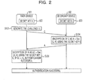
- FIG. 2 is a diagram illustrating an example of a general challenge and response authentication protocol using shared key encryption (1-sided authentication, encrypted and decrypted).
- FIG. 3 is a diagram illustrating an example of a general challenge and response authentication protocol using shared key encryption (1-sided authentication, encrypted only).
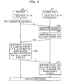
- FIG. 4 is a diagram illustrating an example of a general challenge and response authentication protocol using shared key encryption (2-sided authentication, encrypted and decrypted).
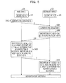
- FIG. 5 is a diagram illustrating an example of a general challenge and response authentication protocol using shared key encryption (2-sided authentication, encrypted only).
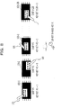
- FIG. 6 is a diagram illustrating an overview of a probe attack.
- FIG. 7A is a diagram illustrating an overview of a shield circuit as a countermeasure against a probe attack.
- FIG. 7B is a diagram illustrating an overview of a shield circuit as a countermeasure against a probe attack.
- FIG. 7C is a diagram illustrating an overview of a shield circuit as a countermeasure against a probe attack.
- FIG. 7D is a diagram illustrating an overview of a shield circuit as a countermeasure against a probe attack.
- FIG. 8 is a diagram illustrating an overview of a shield circuit as a countermeasure against a probe attack.
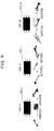
- FIG. 9 is a diagram illustrating an overview of a method using dynamic agitation processing on a key.
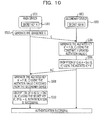
- FIG. 10 is a diagram illustrating an example of a challenge and response authentication (1-sided authentication, encrypted and decrypted) using shared key encryption that uses the method using the dynamic agitation processing on the key.
- FIG. 11 is a diagram illustrating an example of a challenge and response authentication (1-side authentication, encrypted only) using shared key encryption that uses the method using the dynamic agitation method on the key.
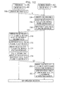
- FIG. 12 is a diagram illustrating an example of a challenge and response authentication (2-sided authentication, encrypted and decrypted) using shared key encryption that uses the method using the dynamic agitation processing on the key.
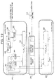
- FIG. 13 is a diagram illustrating an example of a challenge and response authentication (2-sided authentication, encrypted only) using shared key encryption that uses the method using the dynamic agitation processing on the key.
- FIG. 14 is a functional block diagram illustrating a key agitation processing unit for performing dynamic agitation processing on the key using an agitation function F (K, C).
- FIG. 15 is a diagram illustrating a first configuration of the agitation function F (K, C) regarding the key agitation processing unit for performing dynamic agitation processing on a key.
- FIG. 16 is a diagram illustrating an example of a configuration of an optimal asymmetrical encryption encoding processing unit.
- FIG. 17 is a diagram illustrating an example of a key agitation processing unit configured using the optimum asymmetrical encryption encoding processing unit.
- FIG. 18 is a diagram illustrating a second configuration of the agitation function F (K, C) regarding the key agitation processing unit for performing dynamic agitation processing on a key.
- FIG. 19 is a diagram illustrating a second example of a functional block diagram illustrating a key agitation processing unit for performing dynamic agitation processing on a key.
- FIG. 20 is a functional block diagram of a key agitation processing unit for performing dynamic agitation processing on the key including an MGF pre-complication processing unit using a mask generating function MGF.
- FIG. 21 is a diagram illustrating a first configuration of the key agitation processing unit for performing dynamic agitation processing on the key including an MGF pre-complication processing unit using a mask generating function MGF.
- FIG. 22 is a diagram illustrating a second example of the key agitation processing unit for performing dynamic agitation processing on the key including an MGF pre-complication processing unit using a mask generating function MGF.
- FIG. 23 is a first diagram illustrating an overview of a probe attack on the key agitation processing unit for performing dynamic agitation processing on the key including an MGF pre-complication processing using a mask generating function MGF.
- FIG. 24 is a second diagram illustrating an overview of a probe attack on the key agitation processing unit for performing dynamic agitation processing on the key including an MGF pre-complication processing using a mask generating function MGF.
- FIG. 25A is a first diagram describing an example of dynamic agitation processing on the key including an MGF pre-complication processing using a mask generating function MGF.
- FIG. 25B is a second diagram describing an example of dynamic agitation processing on the key including an MGF pre-complication processing using a mask generating function MGF.
- FIG. 26 is a diagram illustrating the nature of a swapping box.
- FIG. 27 is a diagram illustrating an example configuration of a 1-bit swapping box.
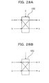
- FIG. 28A is a first diagram illustrating an example of an operation of the 1-bit swapping box.
- FIG. 28B is a second diagram illustrating an example of an operation of the 1-bit swapping box.
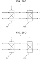
- FIG. 28C is a first diagram illustrating an example of an operation of a multi-stage 1-bit swapping box.
- FIG. 28D is a second diagram illustrating an example of an operation of the multi-stage 1-bit swapping box.
- FIG. 29 is a diagram illustrating an example configuration of a 2-bit swapping box.
- FIG. 30 is a diagram illustrating an example configuration of a multi-stage T-bit swapping box.
- FIG. 31A is a first diagram illustrating the nature of the multi-stage T-bit swapping box.
- FIG. 31B is a second diagram illustrating the nature of the multi-stage T-bit swapping box.
- FIG. 32 is a diagram illustrating the nature of an additive swapping box.
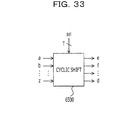
- FIG. 33 is a diagram illustrating the nature of the T-bit swapping box.
- FIG. 34A is a first diagram illustrating an example of the overall configuration of a first and second Embodiment.
- FIG. 34B is a second diagram illustrating an example of the overall configuration of a first and second Embodiment.
- FIG. 35 is a diagram illustrating a configuration example of the MGF pre-complication processing unit according to the first and a fifth Embodiment.
- FIG. 36 is a diagram illustrating an example configuration of a mask processing unit and an unmask processing unit according to the first and the second Embodiment.
- FIG. 37 is a diagram illustrating an example configuration of the MGF pre-complication processing unit according to the second Embodiment.
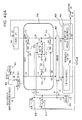
- FIG. 38A is a first diagram illustrating an example of the overall configuration of a third Embodiment.
- FIG. 38B is a second diagram illustrating an example of the overall configuration of a third Embodiment.
- FIG. 39 is a diagram illustrating an example configuration of the MGF pre-complication processing unit according to the third Embodiment.
- FIG. 40 is a diagram illustrating an example configuration of the mask processing unit according to the third Embodiment.
- FIG. 41 is a diagram illustrating an example configuration of the unmask processing unit according to the third Embodiment.
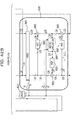
- FIG. 42A is a first diagram illustrating an example of the overall configuration of a fourth Embodiment.
- FIG. 42B is a second diagram illustrating an example of the overall configuration of a fourth Embodiment.
- FIG. 43 is a diagram illustrating an example configuration of the MGF pre-complication processing unit according to the fourth Embodiment.
- FIG. 44 is a diagram illustrating an example configuration of the mask processing unit and the unmask processing unit according to the fourth Embodiment.
- FIG. 45A is a first diagram illustrating an example of the overall configuration of the fifth Embodiment.
- FIG. 45B is a second diagram illustrating an example of the overall configuration of the fifth Embodiment.
- FIG. 46 is an example of a hardware configuration diagram capable of executing the devices of the embodiments.
- Encryption methods are mainly divided into public key encryption methods and shared key encryption methods.
- Public key encryption methods use different keys for encryption and decryption, in which the key for performing encryption (public key) is generally public, and the key for performing decryption of ciphertext (secret key) is designated as private information for only the receiver to preserve safety.
- methods called shared key encryption methods use the same key (secret key) for encryption and decryption, in which the sender and the receiver conceal this secret key from any third party to preserve safety.
- FIG. 1 is a diagram illustrating an overview of a challenge and response authentication protocol.
- an authentication chip 103 includes both a side performing authentication (main device) 101 and a side being authenticated (secondary device) 102.
- a communication protocol called a challenge and response authentication protocol is used to confirm the legitimacy of the devices.
- the challenge and response authentication includes a password using digital information, and the side performing authentication (main device) 101 sends random numbers called the challenge to the side being authenticated (secondary device) 102.
- the secondary device generates a response to the challenge and sends this to the main device.
- the main device determines the value of the response to the challenge, and so determines that the secondary device is a legitimate device if correct.
- FIG. 2 is a diagram illustrating an example of a general challenge and response authentication protocol using shared key encryption (1-sided authentication, encrypted and decrypted).
- the generation of the response corresponding to the challenge is generally a method using encryption functions.
- encryption functions There are different advantages and disadvantages depending on which encryption function is used, but in the case of authentication chips, methods widely used are shared key encryptions which have an advantage of giving priority to decreasing the size of the circuit scale.
- the protocol illustrated in FIG. 2 is pre-sharing a secret key K between the authentication chip 103 in the main device 101 and the authentication chip 103 in the secondary device 102. This is achieved by writing the value of the secret key K at the time of the chip manufacture.
- the important premise from a security viewpoint is that the value of this secret key K is not leaked externally.
- the main device 101 which is the side performing authentication, first generates a challenge called integer G, and transmits this to the secondary device 102, which is the side being authenticated.
- the integer G is a random number.
- the correct response A corresponding to the challenge G may only generated when the secret key K exists, and so the main device 101 is able to confirm the legitimacy of the secondary device 102.
- FIG. 3 is a diagram illustrating an example of a general challenge and response authentication protocol using shared key encryption (1-sided authentication, encrypted only).
- the secret key K is pre-shared between the authentication chip 103 in the main device 101 and the authentication chip 103 in the secondary device 102.
- the main device 101 which is the side performing authentication, generates the integer G called a challenge, and transmits this to the secondary device 102, which is the side being authenticated.
- Enc Enc (G, K)
- FIG. 4 is a diagram illustrating an example of a general challenge and response authentication protocol using shared key encryption (2-sided authentication, encrypted and decrypted).
- the authentication illustrated in FIG. 2 and FIG. 3 is called 1-sided authentication.
- 1-sided authentication is an authentication protocol for confirming the legitimacy of the secondary device 102 by the main device 101.
- the secondary device 102 is not capable of confirming the legitimacy of the main device 101, and so the secondary device 102 may not defend against an invalid main device 101.
- a method for the secondary device 102 to confirm the legitimacy of the main device 101 is preferred.
- An authentication protocol called a 2-sided authentication achieves this.
- the secondary device 102 transmits a challenge to the main device 101, and a processing is performed to confirm the response from the main device 101.
- the main device 101 transmits the challenge G to the secondary device 102.
- the secondary device 102 At a step S304, the secondary device 102 generates a challenge H.
- the challenge H may be an integer or a random number.
- the secondary device 102 transmits the response A and the challenge H to the main device 101.
- the secondary device 102 calculates the response A, which is the result of encrypting the challenge G by the secret key K stored in the authentication chip 103.
- the main device 101 decrypts the response A by the secret key K stored in the authentication chip 103, and determines that the secondary device 102 is legitimate if this matches with the challenge G generated at step S302. Further, the main device 101 generates an integer B, which is the encryption of the challenge H using the secret key K, as the response. Then, the main device 101 sends this response B to the secondary device 102.
- the secondary device 102 decrypts the response B from the main device 101 by the secret key K, and determines that the main device 101 is legitimate if this result matches the challenge H generated at step S304.
- FIG. 5 is a diagram illustrating an example of a general challenge and response authentication protocol using shared key encryption (2-sided authentication, encrypted only).
- the authentication illustrated in FIG. 4 is a 2-sided authentication using encryption and decryption, but authentication using only encryption is also possible.
- the main device 101 generates an integer G as the challenge, and transmits this to the secondary device 102.
- the secondary device 102 At a step S404, the secondary device 102 generates an integer H as the challenge. At a step S406, the secondary device 102 transmits the response A and the challenge H to the main device 101.
- the challenge H may be a random number.
- FIG. 6 is a diagram illustrating an overview of a probe attack.
- the attacker removes the chip package protecting the circuit in the authentication chip 103, and inserts a small electrode called a microprober 105 into the internal wiring. Then, the attacker directly read the value of the key using a sensor 104.
- the probe attack is a powerful method, but it is known that the maximum number of probers provisioned with a reading device using a microprober is limited, and even if many probers are so equipped, the number of microprobers that may be used simultaneously due to physical interference between the microprobers is also limited. That is to say, there is a limit to the number of bits that may be stolen simultaneously by probe attacks.
- probe attacks simultaneously stealing q bits is called a q-bit probe attack.
- FIGs. 7A, 7B , 7C, and 7D are diagrams illustrating an overview of shield circuits functioning as probe attack countermeasures.
- the authentication chip 103 is divided into layers in order from the bottom of the authentication chip 103 towards the top, the layers including an internal circuit B106c, an internal circuit A106b, and a shield circuit 106a (the combinations of these may be referred to as the internal circuit 106).
- the shield circuit 106a is arranged to cover the internal circuit B106c and the internal circuit A106b.
- the wiring called the shield wire is arranged in multiples in the uppermost layer.
- This shield wire functions as a cover against probe intrusions to inhibit intrusions. A certain voltage is applied to each of the shield wires, and when the shield wire is broken, the voltage at the end of the opened shield wire becomes zero. Thus, as the break is detected, the shield circuit 106a may inhibit simple physical modifications.
- FIG. 8 is a diagram illustrating an overview of the shield circuit functioning as a probe attack countermeasure.
- the attacker uses the microprobe 105 to steal one different bit from each of the 128 authentication chips 103_1, 103_2, ..., 103_128 from chip #1 through chip #128. For example, the attacker steals a first key bit value of one (key bit #1) from the first authentication chip 103_1 (authentication chip #1). A second key bit value of zero (key bit #2) is stolen from the second authentication chip 103_2 (authentication chip #2), and a third key bit value of one (key bit #3) is stolen from the third authentication chip 103_3 (authentication chip #3).
- FIG. 9 is a diagram illustrating on overview of a method using dynamic agitation processing of keys.
- the secondary device holds the same key as the main device, and at the same time, holds an agitation value (for example, a random number value) that changes while the power is on (the agitation value is a different value for each secondary device).
- the secondary device encrypts the challenge by an agitation key generated based on the key and the agitation value.
- the secondary device sends the encrypted challenge together with the agitation value to the main device.
- the main device authenticates by decrypting the received, encrypted challenge based on the held key and the received agitation value.
- the main device authenticates by encrypting the challenge by the agitation key generated based on the agitation value and on the key, and comparing this with the encrypted challenge received from the secondary device.
- a different agitation processing is executed on the keys stored in each chip for an N number of authentication chips from #1 to #N labeled as authentication chip 1003_1, 1003_2, ..., 1003_N (the combination of this will be called the authentication chip 1003).
- each authentication chip does not hold a fixed secret key, as the value of the key constantly changed while the power is on.
- the agitation processing is performed on the basis of the value of the secret key stored in the authentication chip 1003 and the agitation value. It is preferable for the agitation value to be different for each authentication chip 1003.
- the agitation value may be a random number that constantly generated while the power is on, or may be a value starting from an initial value different for each authentication chip 1003 to which the authentication chip constantly adds a value of one while the power is on.
- the value produced by agitation using the agitation value different for each authentication chip 1003 corresponding to the shared secret key among the authentication chip 1003 is held internally in the authentication chip 1003. Therefore, as the value of the key at each authentication chip 1003 is observed as a different value, probe attacks against multiple authentication chips 1003 may be inhibited.
- FIG. 10 is a diagram illustrating an example of a challenge and response authentication (1-sided authentication, encrypted and decrypted) using shared key encryption that uses the method using the dynamic agitation method on the key.
- a main device 1001 includes the authentication chip 1003, and a secondary device 1002 includes the authentication chip 1003.
- the authentication chip 1003 stores the secret key K
- the authentication chip 1003 stores the secret key K and the agitation value C.
- the main device 1001 which is the side performing authentication, first generates a challenge called integer G, and transmits this to the secondary device 1002, which is the side being authenticated.
- the integer G may be a random number.
- a receiving unit for receiving the challenge G, which is a random integer, as an input
- a first memory which is non-
- the functions of the main device 1001 and the secondary device 1002 may be interchangeably switched with a combination of the main device 1001 and the secondary device 1002 having the previously described configurations.
- FIG. 11 is a diagram illustrating an example of a challenge and response authentication (1-side authentication, encrypted only) using shared key encryption that uses the method using the dynamic agitation method on the key.
- the main device 1001 which is the side performing authentication, first generates a challenge called integer G, and transmits this to the secondary device 1002, which is the side being authenticated.
- the integer G may be a random number.
- a receiving unit for receiving the challenge G, which is a random integer, as an input
- a first memory which is non-
- the functions of the main device 1001 and the secondary device 1002 may be interchangeably switched with a combination of the main device 1001 and the secondary device 1002 having the previously described configurations.
- FIG. 12 is a diagram illustrating an example of a challenge and response authentication (2-sided authentication, encrypted and decrypted) using shared key encryption that uses the method using the dynamic agitation method on the key.
- the main device 1001 which is the side performing authentication, first generates a challenge called integer G, and transmits this to the secondary device 1002, which is the side being authenticated.
- the integer G may be a random number.
- the secondary device 1002 generates a challenge H.
- the challenge H is an integer, and may be a random number.
- the main device 1001 processing the method illustrated in FIG. 12 receives the agitation value C, the response A, and the second challenge H output by the secondary device 1002, performs an operation of the received agitation value C and a second secret key K, which has the same value as the secret key K stored previously in its own non-volatile memory, in the agitation function F (K, C) to generate the secret key comparison value K', which is an integer, performs an operation of the secret key comparison value K' and the response A in the decryption function Dec (A, K'), which is the reverse function of the encryption function to generate the challenge comparison value Gc, performs an operation of the second agitation value D, which is an integer store in its memory, and the secret key K in the agitation function F (K, D) to generate the second secret comparison value K", which is an integer, compares the challenge G with the challenge comparison result Gc, and when the secondary device 1002 is authenticated based on the results of comparing the challenge G with the challenge comparison value Gc, performs an an
- the key agitation unit in the secondary device 1002 processing the method illustrated in FIG. 12 includes a decryption unit that performs an operation of the secret key K and the second agitation value D in the agitation function F (K, D) to generate the second agitated secret key K", which is an integer, and also performs an operation of the second agitated secret key K" and the second response H in the decryption function Dec (H, K") to generate the second challenge comparison value Hc, and an authenticating unit for authenticating the main device 1001 based on the comparison of the second challenge comparison value Hc and the second challenge H.
- the roles of the main device 1001 and the secondary device 1002 may be interchangeably switched regarding the combination of the main device 1001 and the secondary device 1002 having the previously described configurations.
- FIG. 13 is a diagram illustrating an example of a challenge and response authentication (2-sided authentication, encrypted only) using shared key encryption that uses the method using the dynamic agitation processing on the key.
- the main device 1001 which is the side performing authentication, first generates a challenge called integer G, and transmits this to the secondary device 1002, which is the side being authenticated.
- the integer G may be a random number.
- the secondary device 1002 generates a challenge H.
- the challenge H is an integer, and may be a random number.
- the main device 1001 processing the method illustrated in FIG. 13 receives the agitation value C, the response A, and the second challenge H output by the secondary device 1002, performs an operation of the received agitation value C and a second secret key K, which has the same value as the secret key K stored previously in its own non-volatile memory, in the agitation function F (K, D) to generate the secret key comparison value K', which is an integer, performs an operation of the secret key comparison value K' and the challenge G in the encryption function Enc (G, K') to generate the response comparison value Ac, which is an integer, performs an operation of the second agitation value D, which is an integer stored in its memory, and the secret key K in the agitation function F (K, D) to generate the second agitated secret key K", compares the response A with the response comparison value Ac, and when the secondary device (1002) is authenticated based on the results of comparing the response A with the response comparison value Ac, performs an operation of the second secret key comparison value K" and
- the key agitation unit in the secondary device 1002 processing the method illustrated in FIG. 13 includes a encryption unit that performs an operation of the secret key K and the second agitation value D in the agitation function F (K, D) to generate the second agitated secret key (K"), which is an integer, and also performs an operation of the second agitation value D and the secret key K in the encryption function Enc (K, D) to generate the second response comparison value Bc, and an authenticating unit for authenticating the main device 1001 based on the comparison of the second response B and the second response comparison value Bc.
- the roles of the main device 1001 and the secondary device 1002 may be interchangeably switched regarding the combination of the main device 1001 and the secondary device 1002 having the previously described configurations.
- the following describes (i) classification of countermeasures for probe attacks of non-volatile circuits, (ii) classification of countermeasures for probe attacks of volatile circuits, and (iii) classification of secret key mask calculations.
- Circuits are generally divided into two categories.
- Non-volatile circuits circuits in which reads and writes are both possible, and values are stored at a state when the power is cut or after a reset. Examples include flash ROM, Electrically Erasable Programmable Read-Only Memory (EEPROM), Ferroelectric Random Access Memory (FRAM (registered trademark)), and non-volatile flip flops.
- flash ROM Electrically Erasable Programmable Read-Only Memory
- EEPROM Electrically Erasable Programmable Read-Only Memory
- FRAM Ferroelectric Random Access Memory
- non-volatile flip flops non-volatile flip flops.
- Volatile circuits Circuits in which values are not stored at a state when the power is cut or after a reset. Examples include registers and logic circuits.
- FIG. 14 is a functional block diagram illustrating a key agitation processing unit for performing dynamic agitation processing on the key using an agitation function F (K, C).
- the key agitation processing unit includes a wrapping processing unit 2000, a key storage unit 2100, an unwrapping processing unit 2200, and a bit shortening processing unit 2300.
- the wrapping processing unit 2000 includes a memory 2002 for storing the secret key K, an agitation function operating unit 2004 for performing agitation processing using an agitation function F, a memory 2008 for storing the agitation value C, an agitation value updating unit 2006 for updating the agitation value C stored in the connected memory 2008, and a switcher 2010 for switching between inputs into the agitation function operating unit 2004, whether the input from a device external to the authentication chip 1003 or the agitation value stored in the memory 2008.
- the agitation function operating unit 2004 performs an operation of the secret key K input from the memory 2002 storing the secret key K and the agitation value C input from the switcher 2010 in the agitation function F (K, C).
- the agitation function operating unit 2004 outputs the processing result value F (K, C) to the key storage unit 2100. In this way, at the wrapping processing unit 2000, by performing an operation of the secret key K and the agitation value C in the agitation function F, the key agitation result represented as F (K, C) is generated.
- the key storage unit 2100 is configured by a non-volatile circuit, and includes an agitation key storage unit 2102. Hereafter, the key storage unit 2100 may also be referred to as the non-volatile circuit 2100.
- the agitation key storage unit 2102 stores the value generated by the agitation function operating unit 2004 in the receiving device wrapping processing unit 2000.
- the agitation key storage unit 2102 is connected to the bit shortening processing unit 2300.
- the bit shortening processing unit 2300 shortens the number of bits of the value stored in the agitation key storage unit 2102 as desirable, and outputs this as the agitation key.
- the unwrapping processing unit 2200 includes an inverse function operating unit 2202.
- the inverse function operating unit 2202 uses an inverse agitation function F -1 (K, C) of the agitation function F (K, C) to obtain the secret key K and the agitation value C from the value stored in the agitation key storage unit 2102.
- the secret key K which is the output of the inverse function operating unit 2202, is input and stored into the memory 2002 in the wrapping processing unit 2000.
- the agitated key K' F (K, C) is generated expressed as F (K, C) from the secret key K and agitation value C.
- the agitation key K' is stored in the agitation key storage unit 2102 in the key storage unit 2100, which is configured by a non-volatile circuit.
- the agitation value C is output to a device external to the authentication chip 1003 for synchronizing the main device 1001 and the secondary device 1002 according to an authentication protocols illustrated in FIG. 10 through FIG. 13 . Also, according to these authentication protocols, the main device 1001 or the secondary device 1002 may receive the agitation value C from an external device.
- the agitation value C is a value that is constantly changed while power is running to the chip.
- the content of the processing to update the agitation value is not particularly restricted, and may be an update that is not predictable such as hardware random numbering, or may be an update that is predictable, such as adding a one to the value.
- the agitation function F (K, C) it is desirable for the agitation function F (K, C) to have the following (Nature 1), (Nature 2), and (Nature 3).
- the non-volatile circuit 2100 may satisfy the previously described (Condition 2) "It has to be impossible to steal all bits of the secret key from multiple authentication chips even when a probe attack of Q bits or less is performed repeatedly.”
- the group (K, C) of K and C may be obtained from the agitation key K' stored in the agitation key storage unit 2102.
- the processing to obtain the group (K, C) of K and C from the agitation key K' is performed by volatile circuits such as logical circuits and registers. That is to say, the volatile circuits have the potential to be vulnerable to 1-bit probe attacks on multiple authentication chips. This problem is resolved by using the method ⁇ Countermeasures for Probe Attacks on Volatile Circuits> described later.
- (Nature 3) and (Nature 3') are natures for guaranteeing the difficulty for probe attacks on the non-volatile circuit 2100.
- F (K, C) is 256 bits
- the attacker does not conduct probe attacks simultaneously for the values of the 256 bits which are dynamically updated according to the agitation value C, it is not possible to obtain the group (K, C) of K and C from F (K, C). That is to say, regarding the non-volatile circuit 2100, the previously described (Condition 1) "It has to be impossible to steal all bits of a secret key with regard to a Q-bit probe attack when the maximum number of bits that may be simultaneously stolen by an attacker is designated as Q" may be satisfied.
- the non-volatile circuit 2100 may satisfy the previously described (Condition 1) and (Condition 2).
- the value stored in the non-volatile circuit 2100 may be used directly as the agitation key, or may be used as the agitation key after the bit shortening processing is performed at the bit shortening processing unit 2300.
- FIG. 15 is a diagram illustrating a first configuration of the agitation function F (K, C) regarding the key agitation processing unit for performing dynamic agitation processing on the key.
- the method disclosed in FIG. 15 is based on a public key message padding method called Optimal Asymmetric Encryption Padding (OAEP).
- OAEP Optimal Asymmetric Encryption Padding
- FIG. 16 is a diagram illustrating an example of a configuration of an optimal asymmetrical encryption encoding processing unit.
- FIG. 17 is a diagram illustrating an example of a key agitation processing unit configured using the optimal asymmetrical encryption encoding processing unit.
- the optimal asymmetrical encryption encoding unit in FIG. 16 will be described, and afterwards, the example of a key agitation processing unit configured using the optimal asymmetrical encryption encoding processing unit in FIG. 17 will be described. Afterwards, the description will return to the first configuration of the agitation function F (K, C) in FIG. 15 .
- the optimal asymmetrical encryption encoding unit in FIG. 16 includes a key storage unit 2800, a mask generating function (MGF) operating unit 2702, a mask generating function (MGF) operating unit 2706, a mask generating function (MGF) operating unit 2902, a mask generating function (MGF) operating unit 2906, an XOR gate 2704, an XOR gate 2708, an XOR gate 2904, and an XOR gate 2908.
- the storage unit 2800 is configured by a non-volatile circuit, and further includes a first memory 2802 for storing an agitation key 1 and a second memory 2804 for storing an agitation key 2.
- the mask generating function (MGF) operating unit 2702, the mask generating function (MGF) operating unit 2706, the mask generating function (MGF) operating unit 2902, and the mask generating function (MGF) operating unit 2906 perform an operation of the input in a mask generating function MGF.
- the mask generating function MGF is called a message generating function, and has the following natures.
- the bit length of the input and output may be adjusted by a parameter.
- the mask generating function MGF is basically a hash function that may adjust the bit length of the input and output.
- a seed value seed is input into the mask generating function (MGF) operating unit 2702, and an output MGF (seed) is obtained.
- the output MGF (seed) is input to the XOR gate 2704, and an XOR is calculated with the data value DB to obtain an output DB*MGF (seed).
- MGF mask generating function
- the output DB*MGF (seed) from the XOR gate 2704 is stored in the second memory 2804 in the storage unit 2800. Further, the output DB*MGF (seed) is input into the mask generating function (MGF) operating unit 2706. The result MGF (DB*MGF (seed)) is input into the XOR gate 2708, an XOR is calculated with the seed value seed to obtain an output seed*MGF (DB*MGF (seed)). The output seed*MGF (DB*MGF (seed)) is stored in the first memory 2802 in the storage unit 2800.
- the processing up to this point corresponds to the processing to encrypt the data value DB using the seed value seed.
- the seed*MGF (DB*MGF (seed)) is stored in the first memory 2802 in the storage unit 2800, and the DB*MGF (seed) is stored in the second memory 2804.
- the first item on the left side of the expression above is the value stored in the first memory 2802.
- the second item on the left side is the value obtained by performing the operation of the value stored in the second memory 2804 in the mask generating function (MGF).
- the value stored in the second memory 2804 is input into the mask generating function (MGF) operating unit 2902 to obtain the output MGF DB*MGF (seed). Further, the seed value seed is obtained by an XOR calculation of the output MGF (DB*MGF (seed)) and the seed*MGF (DB*MGF (seed)) value stored in the first memory 2802 performed by the XOR gate 2904.
- MGF mask generating function
- the first item on the left side of the expression above is the value obtained by performing an operation of the output from the XOR gate 2904 in the mask generating function (MGF).
- the second item on the left side is the value stored in the second memory 2804.
- the output from the XOR gate 2904 is input into the mask generating function (MGF) operating unit 2906 to obtain the output MGF (seed).
- an XOR operation is performed by the XOR gate 2908 on the output MGF (seed) from the mask generating function (MGF) operating unit 2906 and the DB*MGF (seed) value stored in the second memory 2804.
- FIG. 17 is a diagram illustrating an example of a key agitation processing unit configured using the optimal asymmetrical encryption encoding processing unit.
- the seed corresponds to the agitation value C in FIG. 14
- the DB corresponds to the secret key K.
- the key agitation processing unit in FIG. 17 includes a wrapping processing unit 3000, a key storage unit 3100, and an unwrapping processing unit 3200.
- the wrapping processing unit 3000 includes a mask generating function (MGF) operating unit 3002, a mask generating function (MGF) operating unit 3006, an XOR gate 3004, and an XOR gate 3008.
- MMF mask generating function
- MMF mask generating function
- the key storage unit 3100 includes a first memory 3102 and a second memory 3104.
- the unwrapping processing unit 3200 includes a mask generating function (MGF) operating unit 3202, a mask generating function (MGF) operating unit 3206, a XOR gate 3204, and a XOR gate 3208.
- MMF mask generating function
- MMF mask generating function
- the agitation value C input into the wrapping processing unit 3000 is constantly updated.
- the agitation value C is input into the mask generating function (MGF) operating unit 3002 to obtain the output MGF (C).
- the output MGF (C) is input into the XOR gate 3004, and an XOR with the secret key K is calculated to obtain the output K*MGF (C).
- the output K*MGF (C) from the XOR gate 3004 is stored in the second memory 3104 in the key storage unit 3100, and at the same time, is input into the mask generating function (MGF) operating unit 3006.
- the result MGF (K*MGF (C)) is input into the XOR gate 3008, and an XOR with the agitation value C is calculated to obtain the output C*MGF (K*MGF (C)).
- the output C*MGF (K*MGF (C)) is stored in the first memory 3102 in the key storage unit 3100.
- the key storage unit 3100 is configured by a non-volatile circuit.
- the value expressed as C*MGF (K* MGF (C)) is stored in the first memory 3102 of the non-volatile circuit, and the value expressed as K*MGF (C) is stored in the second memory 3104.
- the value of the agitation value C may be monitored from a device external to the authentication chip.
- the secret key K is not obtainable.
- the value of the MGF (K*MGF (C)) is a value that is not understood by the attacker as long as probe attacks are not performed on all bits of the secret key K. In this way, the safety of the encryption processing device according to the present embodiment is guaranteed.
- the value K*MGF (C)) is vulnerable against probe attacks when stored in a non-volatile circuit.
- the agitation value C may be monitored from a device external to the authentication chip, and so the attacker is able to calculate the value of MGF (C), probe attacks on the value K*MGF (C) stored in the second memory 3104 are the same as probe attacks on the secret key K which has not been agitated.
- bit combinations are represented by the symbol "
- the key agitation processing unit includes a wrapping processing unit 2300, a key storage unit 2400, and an unwrapping processing unit 2500.
- the high half of the bits of the secret key K are designated as K H
- the low half of the bits of the secret key K are designated as K L
- the high half of the agitation value C are designated as C H
- the low half of the bits of the agitation value C are designated as C L .
- bit combinations are represented by the symbol "
- a memory 2602 stores the K H
- the memory 2602 is connected to an update processing unit 2604.
- the update processing unit 2604 updates the C H , which is the high half bits of the agitation value C stored in the memory 2602.
- a memory 2606 stores the K L
- the memory 2606 is connected to an update processing unit 2608.
- the update processing unit 2608 updates the C L , which is the low half bits of the agitation value C stored in the memory 2606.
- the memory 2602 and memory 2606 are connected to the input terminal of the wrapping processing unit 2300.
- a mask generating function (MGF) operating unit 2302 takes the value of K H
- MGF mask generating function
- the output of the XOR gate 2304 is input into the key storage unit 2400, and at the same time, the mask processing is conducted by a mask generating function (MGF) operating unit 2306. Then, an MGF (K L
- An XOR gate 2308 performs an XOR of the MGF (K L
- the output of the XOR gate 2308 is input into the key storage unit 2400.
- the key storage unit 2400 includes a first agitation key storage unit 2402 and a second agitation key storage unit 2404.
- the first agitation key storage unit 2402 stores the output K H
- the second agitation key storage unit 2404 stores the output K L
- a mask generating function (MGF) operating unit 2502 executes the mask processing on the value K L
- C H )) is generated.
- an XOR gate 2504 an XOR is performed on the MGF (K L
- a mask generating function (MGF) operating unit 2506 the mask processing is conducted on this output K H
- an XOR gate 2508 an XOR is performed on the output MGF (K H
- C L may be stored again in the memory 2602 and the memory 2606, respectively.
- the wrapping processing unit 2300 and the unwrapping processing unit 2500 each include two stages of mask generating function (MGF) operating units.
- the first configuration of the agitation function F (K, C) for the key agitation processing unit illustrated in FIG. 15 may satisfy the (Condition 1) and (Condition 2) regarding non-volatile circuits.
- FIG. 18 is a diagram illustrating a second configuration of the agitation function F (K, C) regarding the key agitation processing unit for performing dynamic agitation processing on the key.
- a wrapping processing unit 3400 and an unwrapping processing unit 3600 both include three stages of mask generating function (MGF) operating units. Also, with the configuration illustrated in FIG. 18 , the division and recombination processing of the secret key K and the agitation value C is not performed, which is different from the configuration illustrated in FIG. 15 .
- the reason for not performing the division and recombination processing of the secret key K and the agitation value C is because an attacker is not able to obtain the value of the key K as long as all bits in the non-volatile circuit are not simultaneously probed. That is to say, it is because the two values stored in the non-volatile circuit as the result of applying the mask generating function (MGF) three times are masked by the mask generating function (MGF) value to which the secret key K was input.
- MMF mask generating function
- the key agitation processing unit includes the wrapping processing unit 3400, a key storage unit 3500, and the unwrapping processing unit 3600.
- the wrapping processing unit 3400 includes a mask generating function (MGF) operating unit 3402, a mask generating function (MGF) operating unit 3406, a mask generating function (MGF) operating unit 3410, an XOR gate 3404, an XOR gate 3408, and an XOR gate 3412.
- MMF mask generating function
- the key storage unit 3100 includes a first memory 3502 and a second memory 3504.
- the unwrapping processing unit 3200 includes a mask generating function (MGF) operating unit 3602, a mask generating function (MGF) operating unit 3606, a mask generating function (MGF) operating unit 3610, the XOR gate 3204, the XOR gate 3208, and an XOR gate 3612.
- MMF mask generating function
- a memory 3702 stores the agitation value C.
- the memory 3702 is connected to an update processing unit 3704.
- the update processing unit 3704 updates the agitation value C stored in the memory 3702.
- a memory 3706 stores the secret key K.
- the memory 3702 and the memory 3706 are connected to the input terminal of the wrapping processing unit 3400.
- the mask processing is conducted by the mask generating function (MGF) operating unit 3402 on the agitation value C input into the wrapping processing unit 3400 from the memory 3702, and the MGF (C) is generated.
- the MGF (C) is input into the XOR gate 3404.
- An XOR is performed on the secret key K and the value input into the wrapping processing unit 3400 from the memory 3706, that is to say, K*MGF (C) is calculated.
- the output of the XOR gate 3404 is input into the XOR gate 3412, and at the same time, the mask processing is conducted by the mask generating function (MGF) operating unit 3406, and an MGF (K*MGF (C)) is generated.
- the XOR gate 3408 performs an XOR of the MGF (K*MGF (C)) and the agitation value C input into the wrapping processing unit 3400 from the memory 3702, and the C*MGF (K*MGF (C)) is calculated.
- the output of the XOR gate 3408 is stored in the first memory 3502 of the key storage unit 3100.
- the mask processing is conducted by the mask generating function (MGF) operating unit 3410 on the C*MGF (K*MGF (C)), and an MGF (C*MGF (K*MGF (C))) is generated.
- the MGF (C*MGF (K*MGF (C))) is input into the XOR gate 3412.
- An XOR is performed on the output K*MGF (C) from the XOR gate 3404 and the MGF (C*MGF (K*MGF (C))), that is to say, the K*MGF (C)* MGF (C*MGF (K*MGF (C))) is calculated.
- the output of the XOR gate 3612 is stored in the second memory 3504 in the key storage unit 3100.
- the key storage unit 3100 is configured by non-volatile memory.
- the first memory 3502 in key storage unit 3100 stores the value C*MGF (K*MGF (C)).
- the second memory 3504 in the key storage unit 3100 stores the value K*MGF (C)*MGF (C*MGF (K*MGF (C))).
- the mask generating function (MGF) operating unit 3602 executes the mask processing on the value C*MGF (K*MGF (C)) stored in the first memory 3502, and MGF (C*MGF (K*MGF (C))) is generated.
- MGF C*MGF (K*MGF (C))
- XOR gate 3604 an XOR is performed on the MGF (C*MGF (K*MGF (C))) and the value K*MGF (C)*MGF (C*MGF (K*MGF (C))) stored in the first memory 3502 to obtain the output K*MGF (C).
- a mask generating function (MGF) operating unit 3606 the mask processing is conducted on this output K*MGF (C) from the XOR gate 3604, and the result MGF (K*MGF (C)) is generated.
- an XOR is performed on the output K*MGF (C) from the mask generating function (MGF) operating unit 3606 and the value C*MGF (K*MGF (C)) stored in the first memory 3502 to obtain the output C.
- the mask processing is conducted by the mask generating function (MGF) operating unit 3610 on the output C from the XOR gate 3608 to generate an MGF (C).
- MGF mask generating function
- FIG. 19 is a diagram illustrating a second example of a functional block diagram illustrating a key agitation processing unit for performing dynamic agitation processing on the key.
- the secret key K (shared key K) is masked by a value called the mask value.
- the mask value uses a V number of values M 0 , M 1 , ..., M v-1 .
- the masked value K*M is stored in a logic circuit.
- the mask value M is different for each authentication chip, and the value is constantly updated while the power is on. Similar to the agitation value, the mask value M is not a value that may be observed from a device external to the authentication chip, the value may only be used within the authentication chip.
- the secret key K is masked by the mask value M, which is dynamically changing, and so the attacker is unable to know the value of the secret key K.
- the V number of mask values M 0 , M 1 , ..., M v-1 have to be observed at the same timing. If this V value is more than the Q as in (Condition 1) and (Condition 2), the attacker is not able to perform probe attacks, and so the (Condition 1) and (Condition 2) may also be satisfied regarding volatile circuits.
- the key agitation processing unit includes a wrapping processing unit 3800, a key storage unit 3900, and an unwrapping processing unit 4000.
- the wrapping processing unit 3800 includes a memory 3802 for storing the value K*M and the V number of mask values M 0 , M 1 , ..., M v-1 , a first update processing unit (mask value update processing unit) 3804 for updating the V number of mask values M 0 , M 1 , ..., M v-1 , a memory 3806 for storing the agitation value C, a second update processing unit (agitation value update processing unit) 3808 for updating the agitation value, a switcher 3810, and an agitation function operating unit F (K, C, M 0 , M 1 , ..., M v-1 ) 3812.
- the agitated secret key F' (K, M 0 , M 1 , ..., M v-1 ) are obtained as output of the agitation function operating unit F (K, C, M 0 , M 1 , ..., M v-1 ) 3812.
- the key storage unit 3900 is configured by a non-volatile circuit, and includes an agitation key storage unit 3902.
- the agitated secret key F' (K, M 0 , M 1 , ..., M v-1 ) is stored in the agitation key storage unit 3902 in the key storage unit 3900.
- the unwrapping processing unit 4000 includes an inverse function operating unit 4002. Using an inverse function agitation function F' -1 (K, M 0 , M 1 , ..., M v-1 ) of the agitation function F' (K, M 0 , M 1 , ..., M v-1 ), the inverse function operating unit 4002 obtains the value K*M and the agitation value C from the value stored in the agitation key storage unit 3902.
- the output K*M from the inverse function operating unit 4002 may be stored in the memory 3802.
- the mask value is a value that may not be observed externally from the chip. That is to say, according to the protocols illustrated in FIG. 10 , FIG. 11 , FIG. 12 , and FIG. 13 , the mask value may not be synchronized between the main device and the secondary device. Authentication based on the mask value, which may not be synchronized, may not be performed. That is to say, regarding the authentication protocols illustrated in FIG. 10 through FIG. 13 , the result of the key agitation processing is not affected by the mask value.
- a key agitation processing including the mask generating function MGF
- the operation of the mask generating function (MGF) on the value of the masked key is affected by all bits of the mask value, and the key agitation processing may produce changes that are not predictable at the main device, which is the side performing authentication.
- the key agitation function F' K, M 0 , M 1 , ..., M v-1
- the key agitation function F' is affected by all bits of the mask value and produces changes which are not predictable, removing the mask value from this calculation result is very difficult.
- the key agitation result expressed by F' (K, M 0 , M 1 , ..., M v-1 ) is not affected by the mask value, and changes only affected by the secret key K and agitation value C.
- the inverse function of the key agitation function F' is expressed as F' -1 (K, M 0 , M 1 , ..., M v-1 ), but the masked secret key K*M is output having been affected by the updated mask values M 0 , M 1 , ..., M v-1 .
- MGF pre-complication processing is a bit transposing processing that determined by the secret key K and the agitation value C.
- FIG. 20 is a functional block diagram of a key agitation processing unit for performing dynamic agitation processing on the key including an MGF pre-complication processing using a mask generating function MGF.
- MGF mask generating function
- the next information describes the inputs and outputs of the MGF pre-complication processing.
- probe attacks on the input side and probe attack on the output side are conceivable.
- the secret key K is masked by the V number of mask values M 0 , M 1 , ..., M v-1 , and so this is made safe by setting the V higher than the Q in (Condition 1) and (Condition 2).
- Probe attacks on the output side are safe due to the nature in which the input value K may not be obtained from the value of P (K, C) even if the agitation value C is known.
- FIG. 21 is a diagram illustrating a first configuration of the key agitation processing unit for performing dynamic agitation processing on the key including an MGF pre-complication processing unit using a mask generating function MGF.
- an input set 4200 is input into an MGF pre-complication processing unit 4202, and an MGF pre-complication processing result P (K, C) 4204 is output. Then, the MGF pre-complication processing result P (K, C) 4204 is input into the mask generating function (MGF) operating unit 4206.
- MGF mask generating function
- an XOR is calculated on the masked secret key K*M and the agitation value C. Afterwards, in order to remove the effect of the mask values M 0 *M 1 ...*M v-1 , the XOR calculation is repeated in the order M 0 , M 1 , ..., M v-1 . Finally, the output K*C is obtained.
- FIG. 22 is a diagram illustrating a second configuration of the key agitation processing unit for performing dynamic agitation processing on the key including an MGF pre-complication processing unit using a mask generating function MGF. According to the key agitation processing unit illustrated in FIG. 22 , a further improvement with a matrix operation has been added to the configuration of the key agitation processing unit illustrated in FIG. 21 .
- an input set 4300 is input into an MGF pre-complication processing unit 4302, and an MGF pre-complication processing result P (K, C) 4304 is output. Then, the MGF pre-complication processing result P (K, C) 4304 is input into the mask generating function (MGF) operating unit 4306.
- MGF mask generating function
- the configuration illustrated in FIG. 22 does not satisfy the previously described condition (Complication 2). Therefore, the configuration illustrated in FIG. 22 does not satisfy the previously described (Condition 1) and (Condition 2).
- FIG. 23 is a first diagram illustrating an overview of a probe attack on the key agitation processing unit for performing dynamic agitation processing on the key including an MGF pre-complication processing using a mask generating function MGF.
- FIG. 24 is a second diagram illustrating an overview of a probe attack on the key agitation processing unit for performing dynamic agitation processing on the key including an MGF pre-complication processing using a mask generating function MGF.
- the linearity or other relationship with the calculation result may be used.
- these configurations are able to satisfy (Condition 3) as the effect of the mask values may be easily removed.
- the relationship between the input and the output of the MGF pre-complication processing is easy for the attacker to formulate, which makes it easy to obtain the input from the output, and so the (Condition 1) and (Condition 2) may not be satisfied. That is to say, according to the MGF pre-complication processing illustrated in FIG. 23 , as illustrated in FIG. 24 , the relational expression between the input and output is definitive and easily attacked.
- an MGF pre-complication processing which simultaneously satisfies both the nature of removing the effect of the mask values, and the nature of not being able to obtain the input from the output, which are difficult to establish together.
- FIG. 25A and FIG. 25B are diagrams describing an example of the key agitation processing unit for performing dynamic agitation processing on the key including an MGF pre-complication processing using a mask generating function MGF.
- a bit transposing processing is executed depending of the value of the secret key K and the agitation value C.
- the relationship of the output regarding the input is changed depending on the exponential number of patterns formed from the bit values of the secret key K and the agitation value C, and so as long as all bit values of the secret key K are not known by the attacker, the relationship of the output regarding the input may not be specified, and so is safe. Also, formulating the bit transposing is difficult, and has an advantage of suppressing attacks.
- the result of the bit transposing processing desirably depends on the values of the secret key K and agitation value C, but there is a restriction in that it may not be dependent on the mask values.
- a circuit described below called a swapping box is used in the MGF pre-complication processing.
- FIG. 26 , FIG. 27 , FIG. 28 , and FIG. 29 are diagrams describing the configuration and nature of the swapping box.
- FIG. 26 is a diagram illustrating the nature of the swapping box.
- FIG. 27 is a diagram illustrating a configuration example of a 1-bit swapping box 4600.
- FIG. 28A is a first diagram illustrating an operation example of a 1-bit swapping box 4700.
- FIG. 28B is a second diagram illustrating an operation example of a 1-bit swapping box 4702.
- FIG. 28C is a first diagram illustrating an operation example of a multi-stage 1-bit swapping box configured from a 1-bit swapping box 4706 and a 1-bit swapping box 4708.
- FIG. 28D is a second diagram illustrating an operation example of a multi-stage 1-bit swapping box configured from a 1-bit swapping box 4710 and a 1-bit swapping box 4712.
- FIG. 29 is a diagram illustrating a configuration example of a 2-bit swapping box 4800.
- the swapping box is a circuit that performs bit transposing depending on a selector signal. Also, it has the following nature.
- the bit transposing result when a (V+1) number of swapping boxes are connected in series, and selector signals K*M, M 0 , M 1 ,..., M v-1 are assigned to each of these is the same as the bit transposing result when the selector signals K*M, M 0 , M 1 , ..., M v-1 are assigned to one swapping box.
- the swapping box When the bit length of the selector signal input into the swapping box is T bits, the swapping box is called a T-bit swapping box.
- FIG. 27A is a diagram illustrating a configuration example of a 1-bit swapping box 4600.
- FIG. 28A is a diagram illustrating an operation example of a 1-bit swapping box.
- FIG. 28B is a diagram illustrating an operation example of a 1-bit swapping box 4702.
- the 1-bit swapping box receives two inputs a and b, and returns outputs X and Y.
- the selector signal is zero, the bit transposing is not executed.
- the selector signal is one, the bit transposing is executed.
- the selector signal has the same nature as the XOR calculation, and as illustrated in FIG. 30 , the bit transposing result from a multi-stage swapping box is equivalent to the bit transposing result from one swapping box when an XOR was calculated on the selector signal.
- FIG. 29 is a diagram illustrating a configuration example of a 2-bit swapping box.
- bit transposing is performed to switch the bit positions of each pair of a and b, and c and d, and when the sel [0] is zero, bit transposing is not performed.
- an arbitrary T-bit swapping box may be easily configured, and the bit transposing result from a multi-stage swapping box is equivalent to the bit transposing result from one swapping box when an XOR was calculated on the selector signal. That is to say, bit transposing dependent on the value of the key is performed, and at the same time, the key mask may be removed, and so the (Condition 1), (Condition 2), and (Condition 3) may be simultaneously satisfied.
- FIG. 30 is a diagram illustrating a configuration example of a multi-stage T-bit swapping box.
- bit transposing dependent on all bit values of the secret key K may be achieved.
- the swapping box processing receiving the effect of all bits of the secret key K is achieved.
- a linear feedback processing is performed as the post processing of the multi-stage swapping box processing repeated for n times.
- the input into the swapping boxes illustrated in FIG. 26 through FIG. 30 may be constants, agitation values, or masked secret key K*M values.
- K*M masked secret key
- FIG. 31A and FIG. 31B are diagrams illustrating the nature of the multi-stage T-bit swapping boxes.
- the result from the XOR calculation of all output from the number of inputs illustrated in FIG. 31A assigned to the swapping box is the same as the output when the XOR calculation values all of these multiple inputs as illustrated in FIG. 31B are assigned to the swapping box.
- the selector signal assigned to the swapping box at this time has to be the same as for the multiple number of inputs.
- the swapping box processing result when the masked secret key K*M is input into the swapping box and the XOR calculation result of the swapping box processing result when each value M 0 , M 1 , ..., M v-1 is input, are the same as the output when the secret key K is assigned to the swapping box.
- swapping boxes illustrated in FIG. 26 through FIG. 29
- FIG. 32 and FIG. 33 Other configuration examples are illustrated in FIG. 32 and FIG. 33 .
- FIG. 32 is a diagram illustrating the nature of an additive swapping box.
- FIG. 33 is a diagram illustrating the nature of the T-bit swapping box.
- the result of bit transposing when a (V + 1) number of swapping boxes are connected in series, and the K*M*M 0 *M 1 , *...*M v-1 for each box is assigned as the selector signal is the same as when K*M, M 0 , M 1 , ..., M v-1 is assigned as the selector signal for one swapping box.
- M K*M*M 0 *M 1 *...*M v-1
- the swapping box having this kind of nature may be achieved by a cyclic shift circuit using the value of the selector signal as a shift bit number. It is obvious that the result of cyclic shifting the data z with the x bit and the result of cyclic shifting with the y bit is the same as the result of cyclic shifting the data z with the x + y bit, and so the bit transposing result of the multi-stage swapping box is the same as the bit transposing result of one swapping box that has added all selector signals for the multi-stage swapping box.
- the embodiment is configured from the combination of the three classes, (i) Classes of Countermeasures for Probe Attacks on Non-Volatile Circuits, (ii) Classes of Countermeasures for Probe Attacks on Volatile Circuits, and (iii) Classes of Mask Calculations of Secret Keys.
- Classes of Countermeasures for Probe Attacks on Non-Volatile Circuits (ii) Classes of Countermeasures for Probe Attacks on Volatile Circuits, and (iii) Classes of Mask Calculations of Secret Keys.
- the first Embodiment is an embodiment of the following combination.
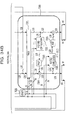
- FIG. 34A and FIG. 34B are diagrams illustrating an example of the overall configuration of a first Embodiment.
- the 128-bit secret key K is divided into a K H of the higher 64 bits and a K L of the lower 64 bits. Masked by a 16-bit mask value M, a data K H * (M
- the 16-bit registers 7009 through 7024 may also function as updating units 7009 through 7024.
- the result of performing the processing to operate the key agitation function F (K, C) on these values is stored in two 128-bit registers, a non-volatile register 7201 and a non-volatile register 7202, and these two values are used as the 128-bit agitation key as the result of the XOR calculation with these two values as the input.
- processing is performed at an MGF pre-complication processing unit 7101, an MGF pre-complication processing unit 7104, an MGF operating unit 7102, an MGF operating unit 7105, an XOR gate 7103, and an XOR gate 7106.
- M), the C L bit combination value, which is the lower 64 bits of the 128-bit agitation value C, and the Mi are input into the MGF pre-complication processing unit 7101.
- the previously described MGF pre-complication processing is performed.
- the result is input into the MGF operating unit 7102.
- the processing is performed so that the processing result is not affected by the Mi values.
- the output of the XOR gate 7103 and the XOR gate 7106 are affected by the 64-bit register 7002 and the 64-bit register 7005, and so are affected by the mask value M.
- the output of the XOR gate 7103 and the XOR gate 7106 are input into an unmasking processing unit 7107, where the unmasking processing is conducted.
- the unmasking processing unit 7107 removes the effect of the mask value M by receiving the M 1 , ..., M 15 and performing a sequential XOR calculation. As a result, this value is stored in the non-volatile flip flop 7201 and 7202, which are not affected by the mask value M.
- the update processing of the agitation value C and the mask value Mi is performed.
- the higher 64 bits of the agitation value C, or C H is executed by an updating unit 7003, and the lower 64 bits of the agitation value C, or C L , is executed by an updating unit 7006.
- the updating of the mask value Mi is executed by updating units 7009 through 7024.
- a masking processing unit 7301 masking of the values stored in the non-volatile flip flop 7201 and the non-volatile flip flop 7202 is performed using the updated mask value Mi.
- This processing is executed by sequentially operating the XOR calculation of the values K H
- processing is performed at an MGF pre-complication processing unit 7303, an MGF pre-complication processing unit 7306, an MGF pre-complication processing unit 7302, an MGF pre-complication processing unit 7305, an XOR gate 7304, and an XOR gate 7307.
- C H )) from the non-volatile flip flop 7202 and the updated mask value Mi is input into the MGF pre-complication processing unit 7302.
- the output from the MGF pre-complication processing unit 7302 is input into the MGF processing unit 7303.
- C H )) from the non-volatile flip flop 7201 and the output from the MGF operating unit 7303 is input into the XOR gate 7304, and an XOR calculation is performed.
- the higher 64 bits of the 128-bit output from the XOR gate 7304 is stored as the new value in the 64-bit register 7001.
- C H )) from the non-volatile flip flop 7201 and the updated mask value Mi is input into the MGF pre-complication processing unit 7305.
- the output from the MGF pre-complication processing unit 7305 is input into the MGF operating unit 7306.
- the XOR gate 7307 performs an XOR calculation on the 128-bit output value obtained from inputting the K L
- the higher 64 bits of the 128-bit output from the XOR gate 7307 is stored as the new value in the 64-bit register 7005.
- the key agitation function F (K, C) is calculated again. Also, the values stored in the non-volatile flip flop 7201 and the non-volatile flip flop 7202 are updated. Also, the updating of the values stored in the 64-bit register 7001 and the 64-bit register 7005 by the calculation processing of F -1 (K, C) are repeated while power to the authentication chip is on.
- Switchers 7007 and 7008 perform the switch processing of the agitation value from the internal registers and external input.
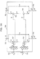
- FIG. 35 is a diagram illustrating a configuration example of a MGF pre-complication processing unit 7400 according to the first Embodiment.
- the configuration illustrated in FIG. 35 applies the MGF pre-complication processing units 7101, 7104, 7302, and 7305 as in FIG. 34 .
- the masked 128-bit data X*M and the 16 values of the 16-bit mask value Mi are input into a terminal 7402 in the MGF pre-complication processing unit 7400.
- the 128-bit constant C is input into a terminal 7401, for example.
- the terminal 7401 is an auxiliary input terminal.
- the MGF pre-complication processing is executed from these inputs to generate the 128-bit output. This output is output from an output terminal 7408.
- the 128-bit data X input into the input terminal 7402 is divided into an XH of the higher 64 bits and an XL of the lower 64 bits, and an XOR calculation of these values is executed by an XOR gate 7419.
- the obtained 64-bit value is further divided into 16 4-bit values, and input into a switcher 7420.
- the output of the switcher 7420 is input into a 4-bit swapping box 7439 and a 4-bit swapping box 7461.
- the 4-bit swapping box 7439 corresponds to a bit transposing processing unit configured of 16 4-bit swapping boxes 7439 through 4-bit swapping boxes 7455 connected in series and a 16-bit linear feedback shift register (LFSR) 7456.
- LFSR linear feedback shift register
- the bit transposing processing is performed at each of the 4-bit swapping boxes 7439 through 4-bit swapping boxes 7455.
- the switcher 7420 assigns the appropriate selector signal for selecting the swapping box, and enables the bit transposing processing repeated 16 times to be executed successfully.
- the 16 16-bit mask values Mi are individually input into terminal 7403 through terminal 7418, divided into 4-bit values, and input into the 16 switcher 7422 through switcher 7437. These switchers output the selector signal for selecting the swapping box so that the bit transposing processing repeated 16 times is executed successfully using the 4-bit swapping box 7439 through the 4-bit swapping box 7455 connected in series and the 16-bit linear feedback shift register (LFSR) 7456.
- LFSR linear feedback shift register
- Processing to repeat the bit transposing processing 16 times is executed at the 4-bit swapping box 7439 through the 4-bit swapping box 7455.
- the bit transposing with the output from the switcher 7420 as the selector signal is performed at the 8 4-bit swapping boxes connected to the switcher 7420 (for example, 4-bit swapping boxes 7439, 7461).
- the selector signal from the switcher 7420 is affected by the mask value, and so the output of the 8 4-bit swapping boxes connected to the switcher 7420 is also affected by the mask value M.
- the 8-serial 16-stage 4-bit swapping boxes including the 4-bit swapping box 7439 through the 4-bit swapping box 7455 and the 4-bit swapping box 7461 through the swapping box 7476 designate the signal generated from the 16 16-bit mask values Mi to be a selector signal, and so the effect of the mask value M may be removed.
- bit transposing processing unit including the 8-serial 16-stage 4-bit swapping boxes and the 16-bit linear feedback shift register (LFSR) is repeated 16 times. Also, the output value of the combining each of the 8-serial 16 bits is affected by the 128-bit data X input from the terminal 7403, and the value that is not affected by the mask value M may be obtained.
- LFSR linear feedback shift register
- FIG. 36 is a diagram illustrating an example configuration of a mask processing unit and an unmask processing unit according to the first Embodiment.
- the mask processing unit and the unmask processing unit share the same configuration.
- the mask processing unit and the unmask processing unit use 16 16-bits mask values M 0 , M 1 , ..., M 15 input into an input terminal 7501 through 7516, an input terminal 7551, and an input terminal 7552, and two 128-bit input values x and y to generate two 128-bit output values X and Y output from an output terminal 7561 and an output terminal 7562.
- Mi is converted by the bit combination of the 16 16-bit mask values M 0 , M 1 , ..., M 15 . Also, an XOR calculation is executed in the order of M0, M1..., M15 on the higher 64 bits of the two 128-bit input values x and y. The result of this XOR calculation and the lower 64 bits of the 128-bit input values x and y are combined to obtain the 128-bit output values X and Y.
- the second Embodiment is an embodiment of the following combination.
- the point that is different between the second Embodiment and the first Embodiment is that the configuration of the swapping boxes is not the configuration in FIG. 30 , but the configuration in FIG. 31 .
- the processing configuration of the MGF pre-complication illustrated in FIG. 35 changes.
- FIG. 34 Similar to the first Embodiment, the overall configuration of the second Embodiment is illustrated in FIG. 34 , and the configuration of the mask processing unit and the unmask processing unit is illustrated in FIG. 36 .
- FIG. 37 is a diagram illustrating an example configuration of the MGF pre-complication processing unit according to the second Embodiment.
- the masked 128-bit data is input from an input terminal 7602, and the 16 16-bit mask values M0, M1, ..., M15 are input from 16 terminals including an input terminal 7603 and input terminal 7604.
- An input terminal 7601 is an auxiliary input terminal.
- a random number generator 7605 generates 128-bit random numbers.
- a 128-bit constant is input into the input terminal 7601.
- a 128-bit output value is generated from the 16 terminals including the input terminal 7602, the input terminal 7603, and the input terminal 7604, the input to the input terminal 7601, and the random number, and the output value is output from the output terminal 7608.
- the MGF pre-complication processing overview 7600 includes two modules, a module 7700 and a module 7800.
- the module 7700 includes an input terminal 7701 through an input terminal 7718
- the module 7800 includes an input terminal 7801 through an input terminal 7818.
- the output of the random number generator 7605 is input into the input terminal 7701 in the module 7700 and the input terminal 7801 in the module 7800.
- the masked 128-bit data input into the input terminal 7602 is input into the input terminal 7702 in the module 7700 and the input terminal 7802 in the module 7800.
- the 16 16-bit mask values M 0 , M 1 , ..., M 15 are input into the 16 input terminals 7703 through input terminals 7718 in the module 7700 and the 16 input terminals 7803 through input terminals 7818 in the module 7800.
- an XOR calculation is performed on the random number generated by the random number generator 7605 and the masked 128-bit data input into the input terminal 7602 by an XOR gate 7606.
- the 128-bit output value from the XOR gate 7606 is input into the input terminal 7801 in the module 7800.
- the output from the module 7700 and the output from the module 7800 are input into an XOR gate 7607. Also, an XOR calculation is performed on the output from the module 7700 and the output from the module 7800 by the XOR gate 7607. The output from the XOR gate 7607 is output from the output terminal 7608.
- FIG. 37 is logically equivalent to FIG. 35 , but the input values into the swapping boxes internal to the module 7700 and the module 7800 are randomized due to the result of the random number generated by the random number generator 7605, which may increase resistance to probe attacks.
- the third Embodiment is an embodiment of the following combination.
- the difference with the first Embodiment is the replacement of the XOR calculation of the mask calculation of the secret key to addition.
- the overall configuration illustrated in FIG. 34 , the MGF pre-complication processing configuration illustrated in FIG. 35 , and the configuration of the mask processing unit and unmask processing unit illustrated in FIG. 36 change.
- the basic structure is the same, but a portion of the calculation replaces the XOR calculation with addition or subtraction.
- FIG. 38A and FIG. 38B are diagrams illustrating examples of an overall configuration of the third Embodiment.
- FIG. 38A and FIG. 38B are basically the same as the embodiment illustrated in FIG. 34A and FIG. 34B .
- the mask processing of the secret key is changed from a form using an XOR calculation to a form using addition. For this reason, a portion of the XOR calculation is replaced with addition and subtraction.
- the mask value M for the secret key are handled in units of 4 bits, the mask values Mi divided 16 times (i is an integer from 0 to 15) are also 4 bits.
- the 128-bit secret key K is divided into K H , which is the higher 64 bits, and K L , which is the lower 64 bits.
- the K H which is the higher 64 bits
- K L which is the lower 64 bits, are each divided every four bits into 16 values K H, 0 , K H, 1 , ..., K H, 15 and K L, 0 , K L, 1 , ..., K L, 15 .
- the 4-bit mask values M are added to produce the masked data (K H, 15 *M)
- the 128-bit agitation value C is divided into the higher 64 bits C H and the lower 64 bits C L , and are stored in a 64-bit register 7902 and a 64-bit register 7905, respectively.
- the 16-bit registers 7909 through 7924 may also function as updating units 7909 through 7924.
- the result of performing the processing to operate the key agitation function F (K, C) on these values is stored in two 128-bit registers, a non-volatile register 8101 and a non-volatile register 8102, and these two values are used as the 128-bit agitation key as the result of the XOR calculation with these two values as the input.
- processing is performed at an MGF pre-complication processing unit 8001, an MGF pre-complication processing unit 8004, an MGF operating unit 8002, an MGF operating unit 8005, an addition gate 8003, and an addition gate 8006.
- (K H, 0 *M) stored in the 64-bit register 7901, the bit combination value of C H , which is the higher 64 bits of the 128-bit agitation value C stored in the 64-bit register 7902, and the Mi are input into the MGF pre-complication processing unit 8001, and the previously described MGF pre-complication processing is performed. This result is input into the MGF operating unit 8002.
- the processing result is processed so that it is not affected by the Mi value.
- the addition gate 8003 the addition calculation is performed on the output from the MGF operating unit 8002, the (K L, 15 *M)
- the output of the addition gate 8003 is input into an unmask processing unit 8007.
- the MGF pre-complication processing is performed by the MGF pre-complication processing unit 8004 on the output from the addition gate 8003, and the MGF is operated by the MGF operation unit 8005.
- the output from the MGF operation unit 8005 is added to the (K H, 15 *M)
- the output of the addition gate 8003 and the addition gate 8006 become the 128-bit input into the unmask processing unit 8007.
- the unmask processing is performed by the unmask processing unit 8007 on the input, and the effect on the value of the masked key is removed by performing a subtraction processing.
- This result which are the values stored in a non-volatile flip flop 8101 and non-volatile flip flop 8102, are not affected by the mask value M.
- the calculation of the key agitation function F (K, C) is completed by the above.
- the update processing is performed on the agitation value C and the mask values K H , 0 , K H,1 , ..., K H, 15 , K L, 0 , K L, 1 , ..., K L, 15 .
- the update of the C H which is the higher 64 bits of the agitation value C, is performed by an updating unit 7903, and the lower 64 bits C L is updated by an updating unit 7906.
- the updating of the mask values K H, 0 , K H, 1 , ..., K L, 15 , K H, 0 , K L, 1 , ..., K L, 15 is executed by an updating unit 7909 through an updating unit 7924.
- the masking of the values stored in the non-volatile flip flop 8101 and the non-volatile flip flop 8102 is performed by a masking processing unit 8201 using the updated mask value Mi.
- This processing is executed by operating the addition calculation of the updated mask value Mi sequentially to the value K H
- processing is performed at an MGF operating unit 8203, an MGF operating unit 8206, an MGF pre-complication processing unit 8202, an MGF pre-complication processing unit 8205, a subtraction gate 8204, and a subtraction gate 8207.
- C H )) from the non-volatile flip flop 8102 and the updated mask value Mi is input into the MGF pre-complication processing unit 8202.
- the output of the MGF pre-complication processing unit 8202 is input into the MGF operating unit 8203.
- C H )) from the non-volatile flip flop 8101 and the output from the MGF operating unit 8203 is input into the subtraction gate 8204, where the subtraction processing is executed.
- the higher 64 bits of the 128-bit output from the subtraction gate 8204 is stored as the new value in the 64-bit register 7901.
- C H )) from the non-volatile flip flop 8101 and the updated mask value Mi is input into the MGF pre-complication processing unit 8205.
- the output of the MGF pre-complication processing unit 8205 is input into the MGF operating unit 8206.
- the subtraction processing is performed by the subtraction gate 8207 on the 128-bit output value obtained by inputting the K L
- the higher 64 bits of the 128-bit output from the subtraction gate 8207 are stored as the new value into the 64-bit register 7905.
- the key agitation function F (K, C) is calculated again.
- the values stored in the non-volatile flip flop 8101 and the non-volatile flip flop 8102 are updated. Also, the updating of the values stored in the 64-bit register 7901 and the 64-bit register 7904 by the subtraction processing of F -1 (K, C) is repeated while the power to the authentication chip is on.
- a switcher 7907 and a switcher 7908 performs processing to switch the agitation value from an internal register to an external input.
- FIG. 39 is a diagram illustrating an example configuration of the MGF pre-complication processing unit according to the third Embodiment.
- the masked 128-bit data X*M and the 16 16-bit mask values Mi are input into a terminal 8302 in an MGF pre-complication processing unit 8300.
- the 128-bit constant C is input into a terminal 8301, for example.
- the terminal 8301 is an auxiliary input terminal.
- the MGF pre-complication processing unit 8300 executes the MGF pre-complication processing from these inputs, and generates the 128-bit output.
- the output may be output from an output terminal 8360.
- the 128-bit data X input into the input terminal 8302 is divided into the higher 64 bits XH and the lower 64 bits XL, and an addition processing is executed on these values by an addition gate 8319.
- the obtained 64-bit value is further divided into 16 4-bit values and input into a switcher 8320.
- the output of the switcher 8320 is input into a 4-bit swapping box 8322 and a 4-bit swapping box 8341.
- the 4-bit swapping box 8322 is the end of a bit transposing processing unit configured from 16 4-bit swapping boxes 8322 through a 4-bit swapping box 8338 connected in series and a 16-bit linear feedback shift register (LFSR) 8339.
- the bit transposing processing is executed 16 times at the 4-bit swapping box 8322 through the 4-bit swapping box 8338.
- Each 4-bit swapping box 8322 through the 4-bit swapping box 8338 is a swapping box related to the addition mask of the secret key K.
- Each 4-bit swapping box 8322 through the 4-bit swapping box 8338 are implemented as 16-bit cyclic shift circuits that perform shifts of only the value of the 4-bit selector signal.
- the switcher 8320 assigns the appropriate selector signal for selecting the swapping box so that the bit transposing processing repeated 16 times is executed successfully.
- Each of the 16 16-bit mask values Mi input into the terminal 8303 through the terminal 8318 are also divided into 4-bit values and input into the 16 4-bit swapping boxes 8322 through the 4-bit swapping box 8338.
- a switcher 8321 outputs the selector signal for selecting the swapping box so that the bit transposing processing repeated 16 times using the 4-bit swapping box 8322 through the 4-bit swapping box 8338 connected in series and the 16-bit linear feedback shift register (LFSR) 8339 is executed successfully when the bit transposing processing is repeated 16 times.
- LFSR linear feedback shift register
- the 8 16-bit values C 0 , C 1 , ..., C 7 are input as 8-serial execution bit transposing processing initial values.
- the bit transposing with the output from the switcher 8320 as the selector signal is performed at the 8 4-bit swapping boxes connected to the switcher 8320 (for example, 4-bit swapping boxes 8322, 8341).
- the selector signal from the switcher 8320 is affected by the mask value, and so the output of the 8 4-bit swapping boxes connected to the switcher 8320 is also affected by the mask value M.
- the 8-serial 16-stage 4-bit swapping boxes including the 4-bit swapping box 8322 through the 4-bit swapping box 8338 and the 4-bit swapping box 8341 through the swapping box 8357 designate the signal generated from the 16 16-bit mask values Mi to be a selector signal, and so the effect of the mask value M may be removed.
- bit transposing processing unit including the 8-serial 16-stage 4-bit swapping boxes and the 16-bit linear feedback shift register (LFSR) is repeated 16 times. Also, the output value of the combining each of the 8-serial 16 bits is affected by the 128-bit data X input from the terminal 8302, and the value that is not affected by the mask value M may be obtained.
- LFSR linear feedback shift register
- FIG. 40 is a diagram illustrating a configuration example of an unmask processing unit according to the third Embodiment.
- An unmask processing unit 8400 receives the 16 4-bit mask values M 0 , M 1 , ..., M 15 input into an input terminal 8401 through an input terminal 8416 and 64-bit input values x and y to be input into an input terminal 8417 through an input terminal 8450. Further, the bit combination value x
- the unmask processing unit 8400 outputs the 128-bit output value X and the output value Y from an output terminal 8480 and an output terminal 8481.
- a processing is performed to sequentially subtract the 4-bit mask values M 0 , M 1 , ..., M 15 from the 64-bit input values x and y to be input into the input terminal 8417, which are divided every 4 bits into 16 4-bit values x 0 , ..., X 15 , y 0 , ..., y 15 .
- the 64-bit value generated from combining the bits of the result of subtracting the 4-bit mask values M 0 , M 1 , ..., M 15 from the 4-bit values x 0 , ..., x 15 , and the 64-bit input value x input into the input terminal 8417 are combined and output from the output terminal 8480.
- the 64-bit value generated from combining the bits of the result of subtracting the 4-bit mask values M 0 , M 1 , ..., M 15 from the 4-bit values y 0 , ..., y 15 , and the 64-bit input value y input into the input terminal 8450 are combined and output from the output terminal 8481.
- FIG. 41 is a diagram illustrating a configuration example of an unmask processing unit according to the third Embodiment.
- An unmask processing unit 8500 receives the 16 4-bit mask values M 0 , M 1 , ..., M 15 input into an input terminal 8501 through an input terminal 8516 and 64-bit input values x and y to be input into an input terminal 8517 through an input terminal 8550. Further, the bit combination value x
- a processing is performed to sequentially subtract the 4-bit mask values M 0 , M 1 , ..., M 15 from the 64-bit input values x and y to be input into the input terminal 8417, which are divided every 4 bits into 16 4-bit values x 0 , ..., x 15 , y 0 , ..., y 15 .
- the 64-bit value generated from combining the bits of the result of subtracting the 4-bit mask values M 0 , M 1 , ..., M 15 from the 4-bit values x 0 , ..., x 15 , and the 64-bit input value x input into the input terminal 8517 are combined and output from the output terminal 8580.
- the 64-bit value generated from combining the bits of the result of subtracting the 4-bit mask values M 0 , M 1 , ..., M 15 from the 4-bit values y 0 , ..., y 15 , and the 64-bit input value y input into the input terminal 8450 are combined and output from the output terminal 8581.
- the fourth Embodiment is an embodiment of the following combination.
- the difference with the first Embodiment is that the configuration in FIG. 18 is used as the countermeasure for probe attacks on non-volatile circuits.
- FIG. 42A and 42B are diagrams illustrating an example of the overall configuration of a fourth Embodiment.
- the agitation value C is stored in a 128-bit register 8601.
- the masked secret key is stored in a 128-bit register 8603.
- M is a 16-bit mask value
- the masked secret key is expressed as K*(M
- the mask value M is not directly stored in a register.
- the 16-bit register 8604 through the 16-bit register 8619 may also function as an updating unit 8604 through an updating unit 8619.
- the result of performing the processing to operate the key agitation function F (K, C) on these values is stored in two 128-bit registers, a non-volatile register 8901 and a non-volatile register 8902.
- processing is performed at an MGF pre-complication processing unit 8704, an MGF operating unit 8701, an MGF operating unit 8703, an MGF operating unit 8706, an XOR gate 8702, and XOR gate 8705, and an XOR gate 8707.
- the agitation value C stored in the 128-bit register 8601 is input into the MGF operating unit 8701.
- the agitation value C is not affected by the mask, and so the MGF pre-complication processing is not valid.
- the addition processing is performed by the XOR gate 8702 on the output of the MGF operating unit 8701 and the output K*(M
- the output of the XOR gate 8702 is input into the MGF pre-complication processing unit 8704.
- the MGF pre-complication processing unit 8704 generates the 128-bit value that is not affected by the mask value Mi from the output of the XOR gate 8702.
- This value is affected by the secret key K and the agitation value C, but is not affected by the mask value M.
- the output of the MGF pre-complication processing unit 8704 is input into the MGF operating unit 8703, and the mask generating function MGF is operated.
- An XOR calculation is conducted in the XOR gate 8705 with the 128-bit output from the MGF operating unit 8703 and the agitation value C, and then input into an unmask processing unit 8800.
- the 128-bit output from the XOR gate 8705 is input into the MGF operating unit 8706, and an XOR calculation is performed in the XOR gate 8707 with the result and the output from the XOR gate 8702.
- the 128-bit output from the XOR gate 8707 is input into the unmask processing unit 8800.
- the two 128-bit input values and the mask value Mi divided into 16 values is input into the unmask processing unit 8800, and using an XOR calculation, generates two values in which the effect of the mask values Mi have been removed from the two 128-bit input values.
- the values C*MGF (K*MGF (C)) and K*MGF (C) *MGF (C*MGF (K*MGF (C))) stored in the non-volatile register 8901 and the non-volatile register 8902 are affected by the secret key K and the agitation value C, but are not affected by the mask value M (or the 16-bit mask values Mi).
- the update processing for the agitation value C and the mask value M is executed.
- the updating of the agitation value C is performed at an updating unit 8602, and the updating of the mask value is performed at an updating unit 8621 and an updating unit 8622.
- the result is an agitation value C stored in the 128-bit register 8601, and updated 16-bit mask values Mi stored in the 16 16-bit registers 8604 through 8619.
- the calculation processing of the inverse agitation function F -1 (K, C) is performed.
- the mask processing is performed at a mask processing unit 9001.
- the mask processing unit 9001 performs the mask processing on the values C*MGF (K*MGF (C)) and K*MGF (C) *MGF (C*MGF (K*MGF (C))) stored in the non-volatile register 8901 and the non-volatile register 8902 using the 16 16-bit mask values Mi stored in the 16 16-bit registers 8604 through the 16-bit register 8619.
- the value C*MGF (K*MGF (C)) stored in the non-volatile register 8901 is output as it is from the mask processing unit 9001.
- an XOR calculation is conducted on to mask the value K*MGF (C) *MGF (C*MGF (K*MGF (C))) stored in the non-volatile register 8902 with the 16 16-bit mask values Mi stored in the 16 16-bit registers 8604 through 8619.
- the input into the MGF operating unit 9002 is not affected by the mask value.
- the output from the MGF operating unit 9002 is input into an XOR gate 9003, where an XOR calculation is performed with the masked value of the K*MGF (C) *MGF (C*MGF (K*MGF (C))) stored in the non-volatile register 8902.
- the output from the XOR gate 9003 is input into an MGF pre-complication processing unit 9004.
- the input into the MGF pre-complication processing unit 9004 is affected by the mask value, but the output is not affected by the mask value.
- the output of the MGF pre-complication processing unit 9004 is input into an MGF operating unit 9005, the MGF is operated and output.
- the output from the MGF operating unit 9005 is not affected by the mask value.
- An XOR calculation is performed at an XOR gate 9006 on the output from the MGF operating unit 9005 with the value C*MGF (K*MGF (C)) stored in the non-volatile register 8901, which is one output from the mask processing unit 9001.
- the XOR calculation result is input into an MGF operating unit 9007, and the MGF is operated.
- An XOR calculation is executed at an XOR gate 9008 on the output from the MGF operating unit 9007 with the output from the XOR gate 9003, and this result is stored in the 128-bit register 8603.
- the key agitation function F (K, C) is calculated again.
- the values stored in the non-volatile register 8901 and the non-volatile register 8902 are updated. Also, the updating of the value stored in the 128-bit register 8603 by the calculation processing of the inverse agitation function F -1 (K, C) is repeated while power to the authentication chip is on.
- a switcher 8623 performs processing to switch the agitation value from the internal register to external input.
- FIG. 43 is a diagram illustrating an example configuration of an MGF pre-complication processing unit according to the fourth Embodiment.
- the masked 128-bit data X*M and the 16 16-bit mask values Mi are input into an MGF pre-complication processing unit 9100 and a terminal 9102 through a terminal 9118.
- the 128-bit constant C is input into a terminal 9101, for example.
- the terminal 9101 is an auxiliary input terminal.
- the MGF pre-complication processing unit 9100 executes the MGF pre-complication processing on these inputs, and generates the 128-bit output. This output is output from an output terminal 9190.
- the 128-bit data X input into the input terminal 9102 is divided into 32 4-bit values X0, ..., X31, and input into a switcher 9119.
- the output from the switcher 9119 is input into 16 4-bit swapping boxes including 4-bit swapping boxes 9137 through 9153.
- the 4-bit swapping box 9137 corresponds to the end of a bit transposing processing unit configured from 16 4-bit swapping boxes 9137 through 9153 connected in series and a 16-bit linear feedback shift register (LFSR) 9154.
- the bit transposing processing is performed at the 16 4-bit swapping boxes 9137 through 9153, repeated for 32 times.
- the bit transposing processing is performed at 8 x 16 4-bit swapping boxes including 4-bit swapping boxes 9161 through 9177.
- Each swapping box is a swapping box related to the mask of the secret key K, and so are implemented as 16-bit cyclic shift circuits that perform shifts of only the value of the 4-bit selector signal.
- the switcher 9119 assigns the appropriate selector signal for selecting the swapping box so that the bit transposing processing repeated 32 times is executed successfully.
- the 16 16-bit mask values Mi input into the terminal 9103 through the terminal 9118 are divided every 4 bits and input into 16 switchers 9120 through a switcher 9135.
- the switcher 9120 through the switcher 9135 send the selector signal to the 8 x 16 4-bit swapping boxes so that the bit transposing processing that is repeated 32 times is processed successfully using the 8 x 16 4-bit swapping boxes including the 4-bit swapping boxes 9137 through 9153, and 9161 through 9177, and the 8 16-bit linear feedback shift registers (LFSR) including 16-bit linear feedback shift register (LFSR) 9154, and a 16-bit linear feedback shift register (LFSR) 9188.
- LFSR linear feedback shift registers
- the bit transposing processing is repeated 32 times using the 8 x 16 4-bit swapping boxes including the 4-bit swapping boxes 9137 through 9153, and 9161 through 9177, and the 8 16-bit linear feedback shift registers (LFSR) including 16-bit linear feedback shift register (LFSR) 9154, and the 16-bit linear feedback shift register (LFSR) 9188.
- LFSR linear feedback shift registers
- the bit transposing is performed at the 8 4-bit swapping boxes connected to each of the 8 switchers to which the 8 16-bit values C 0 , C 1 , ..., and C 7 are input, using the selector signal output from the switchers.
- the selector signal from the switcher 9136 is affected by the mask value, and so the output from the 8 4-bit swapping boxes including the 4-bit swapping box 9137 connected to the switcher 9136 is also affected by the mask value M.
- the 8-serial 16-stage 4-bit swapping boxes including the 4-bit swapping boxes 9137 through 9153 and the 4-bit swapping boxes 9161 through 9187 use the signals generated from the 16 16-bit mask values Mi as selector signals, and so the effect of the mask value M may be removed.
- the processing the by the bit transposing processing unit including these 8-serial 16-stage 4-bit swapping boxes and 16-bit linear feedback shift registers (LFSR) is repeated 32 times.
- the output values from combining the 8-serial 16 bits may be obtained as a value which is affected by the 128-bit data X input into the terminal 9190, and is not affected by the mask value M.
- FIG. 44 is a diagram illustrating an example configuration of a mask processing unit and an unmask processing unit according to the fourth Embodiment.
- the mask processing unit and the unmask processing unit share the same configuration.
- the mask processing unit and unmask processing unit generates two 128-bit output values X and Y to be output from an output terminal 9220 and an output terminal 9221 using the 16 16-bit mask values M 0 , M 1 , ..., M 15 input into input terminals 9203 through 9219, 9201, and 9202, and the two 128-bit input values x and y.
- the 16 16-bit mask values M 0 , M 1 , ..., M 15 are converted by bit combination into a 128-bit value expressed as Mi
- the result of the XOR calculation with y is output from the output terminal 9221 as the 128-bit output Y.
- the result of the XOR calculation with the 128-bit value x input into the input terminal 9201 is output from the output terminal 9220 as the output X.
- the fifth Embodiment is an embodiment of the following combination.
- the basic combination is the same as that of the first Embodiment.
- the difference with the first Embodiment is that the values stored in the non-volatile registers are also masked.
- the values stored in the two non-volatile registers are masked by the same value.
- the mask value is cancelled by using an authentication protocol in which a value obtained by performing an XOR calculation on these two values is used as the agitation key.
- the agitation key is not affected by the mask value.
- the fifth Embodiment is able to further increase resistance to probe attacks.
- the storage place of the M 0 , M 1 .,..., M 15 which is the mask value M divided into 16 portions, has to be changed from a volatile register to a non-volatile register.
- the non-volatile registers are affected by the mask value, if the correct values corresponding mask values are not stored, the correct key value may not be stored.
- the dispersed mask values M 0 , M 1 , ..., M 15 are stored in non-volatile registers.
- FIG. 45A and 45B are diagrams illustrating overall configuration examples of the fifth Embodiment.
- the 128-bit secret key K is divided into a K H , which is the higher 64 bits, and a K L , which is the lower 64 bits.
- the K H and K L are masked by the 16-bit mask values M to produce the data K H * (M
- the 128-bit agitation value C is divided into a C H , which is the higher 64 bits, and a C L , which is the lower 64 bits.
- the C H and C L are stored in a 64-bit register 9302 and a 64-bit register 9305, respectively.
- the 16-bit register 9401 through the 16-bit register 9416 are configured by non-volatile flip flops.
- the 16-bit register 9401 through the 16-bit register 9416 may also function as an updating unit 9401 through an updating unit 9416.
- the result of performing the processing to operate the key agitation function F (K, C) on these values is stored in two 128-bit registers, a non-volatile register 9601 and a non-volatile register 9602, and these two values are used as the 128-bit agitation key as the result of the XOR calculation with these two values as the input.
- processing is performed at an MGF pre-complication processing unit 9501, an MGF pre-complication processing unit 9504, an MGF operating unit 9502, an MGF operating unit 9505, an XOR gate 9503, and an XOR gate 9506.
- M), the C L , which is the lower 64 bits of the 128-bit agitation value C, and the Mi are input into the MGF pre-complication processing unit 9501, where the previously described MGF pre-complication processing is performed. This result is input into the MGF operating unit 9502.
- the processing is performed so that the processing result is not affected by the Mi values.
- the output of the XOR gate 9503 and the XOR gate 9506 are affected by the register 9302 and the register 9305, and so are affected by the mask value M.
- the output of the XOR gate 9503 and the XOR gate 9506 are stored in the non-volatile flip flop 9601 and the non-volatile flip flop 9602 without the unmask processing performed, which is different from the first Embodiment.
- the values stored in the non-volatile flip flop 9601 and the non-volatile flip flop 9602 are both values expressed as M
- the high 64-bit values of the non-volatile register 9601 and non-volatile register 9602 are both affected by the XOR mask of the same value M
- M the XOR mask of the same value
- M the XOR mask of the same value
- the update processing of the agitation value C and the mask value Mi is performed.
- the higher 64 bits of the agitation value C, or C H is executed by an updating unit 9303, and the lower 64 bits of the agitation value C, or C L , is executed by an updating unit 9306.
- the updating of the mask value Mi is executed by updating units 9401 through an updating unit 9416.
- processing is performed at an MGF pre-complication processing unit 9701, an MGF pre-complication processing unit 9704, an MGF operating unit 9702, an MGF operating unit 9705, an XOR gate 9703, and an XOR gate 9706.
- CH)) from the non-volatile flip flop 9702 and the mask value Mi updated by the 8 updating units including the updating unit 9417 and the updating unit 9418 are input into the MGF pre-complication processing unit 9701.
- the output from the MGF pre-complication processing unit 9701 is input into the MGF operating unit 9702.
- the MGF is operated on the input at the MGF operating unit 9702 and output.
- the output from the XOR gate 9703 and the mask value Mi updated by the 8 updating units including the updating unit 9417 and the updating unit 9418 are input into the MGF pre-complication processing unit 9704.
- the output from the MGF pre-complication processing unit 9704 is input into the MGF operating unit 9705.
- an XOR calculation is performed on (K L * (M
- the higher 64 bits of the 128-bit output from the XOR gate 9706 is stored as the new value in the 64-bit register 9304.
- a switcher 9307 and a switcher 9308 perform the switch processing of the agitation value from the internal registers and external input.
- FIG. 46 is an example of a hardware configuration diagram capable of executing the devices of the embodiments.
- each functional block may be configured using a computer configured with standard hardware.
- FIG. 46 is a configuration diagram of an example of computer usable as the encryption processing devices according to the previously described embodiment.
- This computer 9800 is provisioned with an MPU 9801, a ROM 9802, a RAM 9803, a hard disk device 9804, a register 9805, a non-volatile circuit 9806, and an interface device 9807. Further, these configuration components are connected by a bus line 9810, and various data may be sent and received under the management of the MPU 9801.
- the MPU (Micro Processing Unit) 9801 is a calculation processing device for controlling the overall operation of this computer 9800, and functions as the control processing unit of the computer 9800.
- the ROM (Read Only Memory) 9802 is read only semiconductor memory to which a predetermined basic control program has been previously recorded.
- the MPU 9810 is able to control the operation of each configuration element in this computer 9800 by reading out and executing this basic program when the computer 9800 starts up.
- the RAM (Random Access Memory) 9803 is semiconductor memory that may be written to and read from at any time, which is used as a work storage region as desirable by the MPU 9801 when executing various control programs.
- the hard disk device 9804 is a recording device for recording various control programs and various data executed by the MPU 9801.
- the MPU 9801, the ROM 9802, the RAM 9803, the hard disk device 9804, the register 9805, and the non-volatile circuit 9806 configure the control unit.
- the secret key K, the agitation value C, the mask value M, and so on are stored in the register 9805 and the non-volatile 9806.
- the non-volatile circuit 9806 may store the secret key
- the register 9805 may store the agitation value.
- control unit may perform the various processing at the previously described processing units described with reference to FIGs. 10 through 45 .
- the interface device 9807 performs management of the sending and receiving of various information between the various devices connected to this computer 9800. For example, when the present computer 9800 is the main device, this performs management of communication with the secondary device. Also, when the present computer 9800 is the secondary device, this performs management of communication with the main device.
- the interface device 9807 functions as the receiving unit for receiving the random number input as the challenge, and as the transmitting unit for transmitting the agitation value and the response.
- a recording medium drive device 9808 performs readouts of various control programs and data stored in a portable recording medium 9809.
- the MPU 9801 may perform various control processing described later by reading out and executing the predetermined control programs stored in the portable recording medium 9809 via the recording medium drive device 9808.
- examples of the portable recording medium 9809 include flash memory provisioned with connectors of the USB (Universal Serial Bus) specification, CD-ROM (Compact Disc Read Only Memory), DVD-ROM (Digital Versatile Disc Read Only Memory), and others.
- the combination of the MPU 9801, the ROM 9802, the RAM 9803, the register 9805, and the non-volatile circuit 9806 function as the key agitation unit for generating the agitated secret key by operating the agitation function on the secret key and the agitation value, the response generating unit for generating a response by operating an encryption function on a random number using the agitated secret key, and the agitation value updating unit for updating the agitation value.
- a control program is created in which processes are written that enable the MPU 9801 to perform each function block of processing configuring the encryption processing device, for example.
- the created control program is previously stored in the hard disk device 9804 or the portable recording medium 9809. Also, predetermined instructions are assigned to the MPU 9801 to read out and execute this control program. By this designation, the functions provisioned with the encryption processing device are provided by the MPU 9801. Therefore, this computer 9800 may function as the encryption processing device.
Landscapes
- Engineering & Computer Science (AREA)
- Computer Security & Cryptography (AREA)
- Physics & Mathematics (AREA)
- Theoretical Computer Science (AREA)
- Computer Networks & Wireless Communication (AREA)
- Signal Processing (AREA)
- Computer Hardware Design (AREA)
- General Physics & Mathematics (AREA)
- Software Systems (AREA)
- General Engineering & Computer Science (AREA)
- Mathematical Physics (AREA)
- Storage Device Security (AREA)
- Measuring Volume Flow (AREA)
Applications Claiming Priority (1)
| Application Number | Priority Date | Filing Date | Title |
|---|---|---|---|
| JP2012172410A JP5954030B2 (ja) | 2012-08-02 | 2012-08-02 | 暗号処理装置および方法 |
Publications (2)
| Publication Number | Publication Date |
|---|---|
| EP2698780A2 true EP2698780A2 (de) | 2014-02-19 |
| EP2698780A3 EP2698780A3 (de) | 2017-07-05 |
Family
ID=48747933
Family Applications (1)
| Application Number | Title | Priority Date | Filing Date |
|---|---|---|---|
| EP13173773.6A Withdrawn EP2698780A3 (de) | 2012-08-02 | 2013-06-26 | Vorrichtung und Verfahren zur Verschlüsselungsverarbeitung |
Country Status (3)
| Country | Link |
|---|---|
| US (1) | US20140037089A1 (de) |
| EP (1) | EP2698780A3 (de) |
| JP (1) | JP5954030B2 (de) |
Cited By (2)
| Publication number | Priority date | Publication date | Assignee | Title |
|---|---|---|---|---|
| CN105119900A (zh) * | 2015-07-17 | 2015-12-02 | 北京奇虎科技有限公司 | 信息安全传输方法、联网接入方法及相应的终端 |
| CN109257630A (zh) * | 2018-11-14 | 2019-01-22 | 苏州科达科技股份有限公司 | 视频点播中的数据传输系统、方法、装置及存储介质 |
Families Citing this family (13)
| Publication number | Priority date | Publication date | Assignee | Title |
|---|---|---|---|---|
| IT1264065B1 (it) | 1993-04-09 | 1996-09-10 | Cedal Srl | Assemblatrice automatica di pacchetti per laminati plastici ottenuti da nastri metallici continui |
| US9787568B2 (en) * | 2012-11-05 | 2017-10-10 | Cercacor Laboratories, Inc. | Physiological test credit method |
| JP6059347B2 (ja) * | 2013-07-18 | 2017-01-11 | 日本電信電話株式会社 | 復号装置、復号能力提供装置、それらの方法、およびプログラム |
| US10367803B2 (en) * | 2015-04-12 | 2019-07-30 | Gropper Adrian | Managed open source medical devices |
| JP2017076854A (ja) * | 2015-10-14 | 2017-04-20 | 富士通株式会社 | 電子装置、及びデータ検証方法 |
| US10853523B2 (en) * | 2016-03-22 | 2020-12-01 | New York University In Abu Dhabi Corporation | System, method and computer-accessible medium for satisfiability attack resistant logic locking |
| MX386209B (es) * | 2016-10-27 | 2025-03-18 | Hewlett Packard Development Co | Autentificación de elemento reemplazable. |
| EP3373178B1 (de) | 2017-03-08 | 2024-09-18 | Secure-IC SAS | Vergleich von ausführungkontextdaten signaturen mit referenzen |
| EP4368104A3 (de) | 2017-04-28 | 2024-09-25 | Masimo Corporation | Punktprüfmesssystem |
| US11296896B2 (en) * | 2018-03-30 | 2022-04-05 | Canon Kabushiki Kaisha | Method of authenticating authentication-target apparatus using challenge and response |
| KR102025569B1 (ko) * | 2019-01-31 | 2019-11-04 | 김동현 | 재생 카트리지에 설치되는 인증용 메모리 모듈 |
| US11218320B2 (en) * | 2019-06-28 | 2022-01-04 | Intel Corporation | Accelerators for post-quantum cryptography secure hash-based signing and verification |
| US11575521B2 (en) | 2019-06-28 | 2023-02-07 | Intel Corporation | Fast XMSS signature verification and nonce sampling process without signature expansion |
Family Cites Families (13)
| Publication number | Priority date | Publication date | Assignee | Title |
|---|---|---|---|---|
| JPH104403A (ja) * | 1996-06-17 | 1998-01-06 | N T T Data Tsushin Kk | 暗号化装置、復号化装置およびその方法 |
| US5828753A (en) * | 1996-10-25 | 1998-10-27 | Intel Corporation | Circuit and method for ensuring interconnect security within a multi-chip integrated circuit package |
| WO1998051029A1 (en) * | 1997-05-07 | 1998-11-12 | Southwestern Bell Telephone Company | Apparatus and method for customized secondary access authentication |
| JPH11252069A (ja) * | 1998-03-06 | 1999-09-17 | Fuji Electric Co Ltd | 情報機器間の相互認証装置 |
| JPH11305661A (ja) * | 1998-04-23 | 1999-11-05 | Toyo Commun Equip Co Ltd | シフトレジスタ構成用回路およびシフトレジスタ |
| US6243811B1 (en) * | 1998-07-31 | 2001-06-05 | Lucent Technologies Inc. | Method for updating secret shared data in a wireless communication system |
| JP2002015512A (ja) * | 1999-07-15 | 2002-01-18 | Matsushita Electric Ind Co Ltd | デジタルデータ書込装置、デジタルデータ記録装置、デジタルデータ利用装置 |
| FR2820577B1 (fr) * | 2001-02-08 | 2003-06-13 | St Microelectronics Sa | Procede securise de calcul cryptographique a cle secrete et composant mettant en oeuvre un tel procede |
| US7034654B2 (en) * | 2004-01-13 | 2006-04-25 | General Motors Corporation | Motor vehicle engine immobilizer security system and method |
| US9497022B2 (en) * | 2005-05-24 | 2016-11-15 | Broadcom Corporation | Method and system for improved fault tolerance in distributed customization controls using non-volatile memory |
| DE102009024604B4 (de) * | 2009-06-10 | 2011-05-05 | Infineon Technologies Ag | Erzeugung eines Session-Schlüssels zur Authentisierung und sicheren Datenübertragung |
| JP5446650B2 (ja) * | 2009-09-17 | 2014-03-19 | 沖電気工業株式会社 | 通信データ新規性確認システム並びに送信端末及び受信端末 |
| US8614950B2 (en) * | 2010-11-30 | 2013-12-24 | Marvell Israel (M.I.S.L) Ltd. | Load balancing hash computation for network switches |
-
2012
- 2012-08-02 JP JP2012172410A patent/JP5954030B2/ja not_active Expired - Fee Related
-
2013
- 2013-06-17 US US13/919,299 patent/US20140037089A1/en not_active Abandoned
- 2013-06-26 EP EP13173773.6A patent/EP2698780A3/de not_active Withdrawn
Non-Patent Citations (1)
| Title |
|---|
| MIHIR BELLARE; PHILLIP ROGAWAY: "EUROCRYPT '94, LNCS", vol. 950, 1995, SPRINGER, article "Optimal Asymmetric Encryption: How to Encrypt with RSA", pages: 341 - 358 |
Cited By (4)
| Publication number | Priority date | Publication date | Assignee | Title |
|---|---|---|---|---|
| CN105119900A (zh) * | 2015-07-17 | 2015-12-02 | 北京奇虎科技有限公司 | 信息安全传输方法、联网接入方法及相应的终端 |
| CN105119900B (zh) * | 2015-07-17 | 2019-02-26 | 北京奇虎科技有限公司 | 信息安全传输方法、联网接入方法及相应的终端 |
| CN109257630A (zh) * | 2018-11-14 | 2019-01-22 | 苏州科达科技股份有限公司 | 视频点播中的数据传输系统、方法、装置及存储介质 |
| CN109257630B (zh) * | 2018-11-14 | 2020-12-11 | 苏州科达科技股份有限公司 | 视频点播中的数据传输系统、方法、装置及存储介质 |
Also Published As
| Publication number | Publication date |
|---|---|
| US20140037089A1 (en) | 2014-02-06 |
| EP2698780A3 (de) | 2017-07-05 |
| JP2014033324A (ja) | 2014-02-20 |
| JP5954030B2 (ja) | 2016-07-20 |
Similar Documents
| Publication | Publication Date | Title |
|---|---|---|
| EP2698780A2 (de) | Vorrichtung und Verfahren zur Verschlüsselungsverarbeitung | |
| Clulow | On the security of PKCS# 11 | |
| US9648026B2 (en) | Cryptographic method for securely exchanging messages and device and system for implementing this method | |
| US10790962B2 (en) | Device and method to compute a block cipher | |
| EP3169017B1 (de) | Split-and-merge-ansatz zum schutz gegen dfa-angriffe | |
| EP3363142B1 (de) | Kryptografische vorrichtung und codierungsvorrichtung | |
| EP2957062A1 (de) | Implementierung eines manipulationssicheren kryptografischen algorithmus | |
| WO2022237440A1 (en) | Authenticated encryption apparatus with initialization-vector misuse resistance and method therefor | |
| Gebotys | Security in embedded devices | |
| CN119602946A (zh) | 一种后量子密码与国密算法混合加密、解密方法和设备 | |
| CN105763322B (zh) | 一种可混淆的加密密钥隔离数字签名方法及系统 | |
| Kelber et al. | General design rules for chaos-based encryption systems | |
| RU2710670C2 (ru) | Криптографическая система и способ | |
| JP6890589B2 (ja) | 計算デバイス及び方法 | |
| Dreyer et al. | ESPuF–enabling SRAM PUFs on commodity hardware | |
| CN111314051A (zh) | 一种加解密方法和装置 | |
| KR102803454B1 (ko) | 부가 비밀키를 이용한 암호문의 복호화 방법 및 장치 | |
| KR20110100454A (ko) | 키 암호화 및 셔플링이 적용된 부채널 공격에 안전한 키 관리방법 | |
| JP2015534415A (ja) | メッセージへの全単射アルゴリズムの適用によるコードの真正性を制御するための制御方法およびデバイス | |
| US12021973B2 (en) | System and method for post-quantum trust provisioning and updating with contemporary cryptography | |
| Gomathisankaran et al. | Glitch resistant private circuits design using HORNS | |
| CN111314079A (zh) | 一种加解密方法、装置 |
Legal Events
| Date | Code | Title | Description |
|---|---|---|---|
| AK | Designated contracting states |
Kind code of ref document: A2 Designated state(s): AL AT BE BG CH CY CZ DE DK EE ES FI FR GB GR HR HU IE IS IT LI LT LU LV MC MK MT NL NO PL PT RO RS SE SI SK SM TR |
|
| AX | Request for extension of the european patent |
Extension state: BA ME |
|
| PUAI | Public reference made under article 153(3) epc to a published international application that has entered the european phase |
Free format text: ORIGINAL CODE: 0009012 |
|
| PUAL | Search report despatched |
Free format text: ORIGINAL CODE: 0009013 |
|
| AK | Designated contracting states |
Kind code of ref document: A3 Designated state(s): AL AT BE BG CH CY CZ DE DK EE ES FI FR GB GR HR HU IE IS IT LI LT LU LV MC MK MT NL NO PL PT RO RS SE SI SK SM TR |
|
| AX | Request for extension of the european patent |
Extension state: BA ME |
|
| RIC1 | Information provided on ipc code assigned before grant |
Ipc: H04L 9/08 20060101ALI20170526BHEP Ipc: H04L 9/32 20060101ALI20170526BHEP Ipc: H04L 9/00 20060101ALI20170526BHEP Ipc: G09C 1/00 20060101AFI20170526BHEP |
|
| 17P | Request for examination filed |
Effective date: 20171116 |
|
| RBV | Designated contracting states (corrected) |
Designated state(s): AL AT BE BG CH CY CZ DE DK EE ES FI FR GB GR HR HU IE IS IT LI LT LU LV MC MK MT NL NO PL PT RO RS SE SI SK SM TR |
|
| STAA | Information on the status of an ep patent application or granted ep patent |
Free format text: STATUS: THE APPLICATION IS DEEMED TO BE WITHDRAWN |
|
| 18D | Application deemed to be withdrawn |
Effective date: 20180106 |