EP2690534A2 - Touch screen panel and fabrication method thereof - Google Patents
Touch screen panel and fabrication method thereof Download PDFInfo
- Publication number
- EP2690534A2 EP2690534A2 EP12197629.4A EP12197629A EP2690534A2 EP 2690534 A2 EP2690534 A2 EP 2690534A2 EP 12197629 A EP12197629 A EP 12197629A EP 2690534 A2 EP2690534 A2 EP 2690534A2
- Authority
- EP
- European Patent Office
- Prior art keywords
- sensing cells
- sensing
- lines
- connecting lines
- touch screen
- Prior art date
- Legal status (The legal status is an assumption and is not a legal conclusion. Google has not performed a legal analysis and makes no representation as to the accuracy of the status listed.)
- Granted
Links
- 238000000034 method Methods 0.000 title claims description 24
- 238000004519 manufacturing process Methods 0.000 title claims description 14
- 230000008878 coupling Effects 0.000 claims abstract description 22
- 238000010168 coupling process Methods 0.000 claims abstract description 22
- 238000005859 coupling reaction Methods 0.000 claims abstract description 22
- 239000000463 material Substances 0.000 claims description 20
- 239000004020 conductor Substances 0.000 claims description 18
- AMGQUBHHOARCQH-UHFFFAOYSA-N indium;oxotin Chemical compound [In].[Sn]=O AMGQUBHHOARCQH-UHFFFAOYSA-N 0.000 claims description 11
- 238000000059 patterning Methods 0.000 claims description 7
- VYPSYNLAJGMNEJ-UHFFFAOYSA-N Silicium dioxide Chemical compound O=[Si]=O VYPSYNLAJGMNEJ-UHFFFAOYSA-N 0.000 description 8
- 238000012800 visualization Methods 0.000 description 7
- 238000005530 etching Methods 0.000 description 6
- 239000000377 silicon dioxide Substances 0.000 description 4
- 229920002284 Cellulose triacetate Polymers 0.000 description 2
- 239000004642 Polyimide Substances 0.000 description 2
- 229910052581 Si3N4 Inorganic materials 0.000 description 2
- NNLVGZFZQQXQNW-ADJNRHBOSA-N [(2r,3r,4s,5r,6s)-4,5-diacetyloxy-3-[(2s,3r,4s,5r,6r)-3,4,5-triacetyloxy-6-(acetyloxymethyl)oxan-2-yl]oxy-6-[(2r,3r,4s,5r,6s)-4,5,6-triacetyloxy-2-(acetyloxymethyl)oxan-3-yl]oxyoxan-2-yl]methyl acetate Chemical compound O([C@@H]1O[C@@H]([C@H]([C@H](OC(C)=O)[C@H]1OC(C)=O)O[C@H]1[C@@H]([C@@H](OC(C)=O)[C@H](OC(C)=O)[C@@H](COC(C)=O)O1)OC(C)=O)COC(=O)C)[C@@H]1[C@@H](COC(C)=O)O[C@@H](OC(C)=O)[C@H](OC(C)=O)[C@H]1OC(C)=O NNLVGZFZQQXQNW-ADJNRHBOSA-N 0.000 description 2
- 230000006866 deterioration Effects 0.000 description 2
- 229920003229 poly(methyl methacrylate) Polymers 0.000 description 2
- 229920000139 polyethylene terephthalate Polymers 0.000 description 2
- 239000005020 polyethylene terephthalate Substances 0.000 description 2
- 229920001721 polyimide Polymers 0.000 description 2
- 239000004926 polymethyl methacrylate Substances 0.000 description 2
- 230000035945 sensitivity Effects 0.000 description 2
- 235000012239 silicon dioxide Nutrition 0.000 description 2
- HQVNEWCFYHHQES-UHFFFAOYSA-N silicon nitride Chemical compound N12[Si]34N5[Si]62N3[Si]51N64 HQVNEWCFYHHQES-UHFFFAOYSA-N 0.000 description 2
- 239000012780 transparent material Substances 0.000 description 2
- 238000000137 annealing Methods 0.000 description 1
- 125000004122 cyclic group Chemical group 0.000 description 1
- 230000008021 deposition Effects 0.000 description 1
- 238000013461 design Methods 0.000 description 1
- 239000011521 glass Substances 0.000 description 1
- 239000007769 metal material Substances 0.000 description 1
- 238000012986 modification Methods 0.000 description 1
- 230000004048 modification Effects 0.000 description 1
- 229920000515 polycarbonate Polymers 0.000 description 1
- 239000004417 polycarbonate Substances 0.000 description 1
- 229920000098 polyolefin Polymers 0.000 description 1
- 238000012545 processing Methods 0.000 description 1
Images


Classifications
-
- G—PHYSICS
- G06—COMPUTING; CALCULATING OR COUNTING
- G06F—ELECTRIC DIGITAL DATA PROCESSING
- G06F3/00—Input arrangements for transferring data to be processed into a form capable of being handled by the computer; Output arrangements for transferring data from processing unit to output unit, e.g. interface arrangements
- G06F3/01—Input arrangements or combined input and output arrangements for interaction between user and computer
- G06F3/03—Arrangements for converting the position or the displacement of a member into a coded form
- G06F3/041—Digitisers, e.g. for touch screens or touch pads, characterised by the transducing means
- G06F3/044—Digitisers, e.g. for touch screens or touch pads, characterised by the transducing means by capacitive means
- G06F3/0443—Digitisers, e.g. for touch screens or touch pads, characterised by the transducing means by capacitive means using a single layer of sensing electrodes
-
- G—PHYSICS
- G06—COMPUTING; CALCULATING OR COUNTING
- G06F—ELECTRIC DIGITAL DATA PROCESSING
- G06F3/00—Input arrangements for transferring data to be processed into a form capable of being handled by the computer; Output arrangements for transferring data from processing unit to output unit, e.g. interface arrangements
- G06F3/01—Input arrangements or combined input and output arrangements for interaction between user and computer
- G06F3/03—Arrangements for converting the position or the displacement of a member into a coded form
- G06F3/041—Digitisers, e.g. for touch screens or touch pads, characterised by the transducing means
- G06F3/044—Digitisers, e.g. for touch screens or touch pads, characterised by the transducing means by capacitive means
-
- H—ELECTRICITY
- H03—ELECTRONIC CIRCUITRY
- H03K—PULSE TECHNIQUE
- H03K17/00—Electronic switching or gating, i.e. not by contact-making and –breaking
- H03K17/94—Electronic switching or gating, i.e. not by contact-making and –breaking characterised by the way in which the control signals are generated
- H03K17/96—Touch switches
- H03K17/9618—Touch switches using a plurality of detectors, e.g. keyboard
-
- H—ELECTRICITY
- H03—ELECTRONIC CIRCUITRY
- H03K—PULSE TECHNIQUE
- H03K17/00—Electronic switching or gating, i.e. not by contact-making and –breaking
- H03K17/94—Electronic switching or gating, i.e. not by contact-making and –breaking characterised by the way in which the control signals are generated
- H03K17/965—Switches controlled by moving an element forming part of the switch
- H03K17/975—Switches controlled by moving an element forming part of the switch using a capacitive movable element
-
- H—ELECTRICITY
- H05—ELECTRIC TECHNIQUES NOT OTHERWISE PROVIDED FOR
- H05K—PRINTED CIRCUITS; CASINGS OR CONSTRUCTIONAL DETAILS OF ELECTRIC APPARATUS; MANUFACTURE OF ASSEMBLAGES OF ELECTRICAL COMPONENTS
- H05K3/00—Apparatus or processes for manufacturing printed circuits
-
- G—PHYSICS
- G06—COMPUTING; CALCULATING OR COUNTING
- G06F—ELECTRIC DIGITAL DATA PROCESSING
- G06F2203/00—Indexing scheme relating to G06F3/00 - G06F3/048
- G06F2203/041—Indexing scheme relating to G06F3/041 - G06F3/045
- G06F2203/04103—Manufacturing, i.e. details related to manufacturing processes specially suited for touch sensitive devices
-
- G—PHYSICS
- G06—COMPUTING; CALCULATING OR COUNTING
- G06F—ELECTRIC DIGITAL DATA PROCESSING
- G06F2203/00—Indexing scheme relating to G06F3/00 - G06F3/048
- G06F2203/041—Indexing scheme relating to G06F3/041 - G06F3/045
- G06F2203/04111—Cross over in capacitive digitiser, i.e. details of structures for connecting electrodes of the sensing pattern where the connections cross each other, e.g. bridge structures comprising an insulating layer, or vias through substrate
-
- Y—GENERAL TAGGING OF NEW TECHNOLOGICAL DEVELOPMENTS; GENERAL TAGGING OF CROSS-SECTIONAL TECHNOLOGIES SPANNING OVER SEVERAL SECTIONS OF THE IPC; TECHNICAL SUBJECTS COVERED BY FORMER USPC CROSS-REFERENCE ART COLLECTIONS [XRACs] AND DIGESTS
- Y10—TECHNICAL SUBJECTS COVERED BY FORMER USPC
- Y10T—TECHNICAL SUBJECTS COVERED BY FORMER US CLASSIFICATION
- Y10T29/00—Metal working
- Y10T29/49—Method of mechanical manufacture
- Y10T29/49002—Electrical device making
- Y10T29/49117—Conductor or circuit manufacturing
- Y10T29/49124—On flat or curved insulated base, e.g., printed circuit, etc.
- Y10T29/49155—Manufacturing circuit on or in base
Definitions
- aspects of the present invention relate to a touch screen panel and a fabrication method thereof.
- a touch screen panel is an input device capable of inputting a user's instruction by selecting instruction contents displayed on a screen of an image display device, or the like, with a human hand or an object.
- the touch screen panel may be provided on a front surface of the image display device to convert a contact position directly contacted by the human hand or the object into an electric signal. Therefore, the instruction contents selected at the contact position may be recognized as an input signal.
- the touch screen panel may be substituted for a separate input device connected to the image display device, such as a keyboard or a mouse, application fields thereof have been gradually extended.
- Example types of the touch screen panel include a resistive type touch screen panel, a photosensitive type touch screen panel, a capacitive type touch screen panel, and the like.
- the capacitive type touch screen panel senses a change in capacitance formed between a conductive sensing pattern and neighboring other sensing patterns, a ground electrode, or the like, when a human hand or an object contacts the touch screen panel, thereby converting a contact position into an electric signal.
- the capacitive type touch screen panel may include first sensing cells coupled to each other and formed in a first direction, and second sensing cells coupled to each other and formed in a second direction.
- adjacent first sensing cells may be electrically connected to each other through a first connecting line
- adjacent second sensing cells may be electrically connected to each other through a second connecting line
- the first and second connecting lines may overlap each other (but are insulated by an insulating layer interposed therebetween).
- first and second sensing cells are formed on the same layer and the first or second connecting lines are formed on the insulating layer in a bridge pattern to couple the first or second sensing cells to each other, respectively, has been used.
- the connecting lines formed on the insulating layer may be made of the same material as that of the sensing cell, for example, a transparent conductive material (such as, an indium tin oxide (ITO), or a low resistance metal material).
- a transparent conductive material such as, an indium tin oxide (ITO), or a low resistance metal material.
- the bridge pattern may be observed (or viewed), which may interfere with an image displayed on the image display device.
- the quantity of material used in the bridge pattern and/or dimensions of length, width, and thickness thereof may be reduced (e.g., made as small as possible).
- such a design increases resistance of the bridge pattern, which causes other problems, such as a deterioration of sensing sensitivity and vulnerability to external electrostatic discharge (ESD).
- An aspect of an embodiment according to the present invention is to provide a touch screen panel capable of preventing (or reducing) observation of patterns and reducing resistance of connecting lines by implementing first and second sensing cells, configuring sensing patterns in a stacked structure, and/or forming the connecting lines coupling first sensing cells to each other integrally with an upper layer of the first sensing cells, and a fabrication method thereof.
- an embodiment of the present invention provides a touch screen panel including: sensing patterns in a display region of a transparent base; and sensing lines in a non-display region positioned at an outer side of the display region and coupled to the sensing patterns.
- the sensing patterns include: a plurality of first sensing cells in a plurality of first lines in a first direction; first connecting lines coupling the first sensing cells in corresponding first lines from among the plurality of first lines to each other; second sensing cells in a plurality of second lines in a second direction; and second connecting lines coupling the second sensing cells in corresponding second lines from among the plurality of second lines to each other, and the first sensing cells and the second sensing cells each have a stacked structure, and the first connecting lines are integral with an upper layer of the first sensing cells.
- Portions of the first connecting lines may overlap portions of the second connecting lines, and an insulating layer may be at a region between the first connecting lines and the second connecting lines.
- Each first sensing cell may include: a lower first sensing cell at a lower portion thereof; and an upper first sensing cell at an upper portion thereof
- each second sensing cell may include: a lower second sensing cell at a lower portion thereof; and an upper second sensing cell at an upper portion thereof.
- the first connecting lines are integral with the upper first sensing cells that are adjacent in the first direction
- the second connecting lines are integral with the upper second sensing cells that are adjacent in the second direction.
- the first connecting lines and the upper first sensing cells may have thicknesses smaller than that of the lower first sensing cells.
- the first sensing cells, the second sensing cells, the first connecting lines, and the second connecting lines may all be made of the same material.
- the same material is a crystalline indium tin oxide (ITO).
- a method of fabricating a touch screen panel including: forming a plurality of lower first sensing cells in a display region of a transparent base in a plurality of first lines in a first direction; forming a plurality of lower second sensing cells in the display region of the transparent base in a plurality of second lines in a second direction; forming a plurality of second connecting lines coupling together the lower second sensing cells in corresponding second lines; forming an insulating layer on the second connecting lines; forming a transparent conductive material to cover a region of the transparent base on which the lower first sensing cells, the lower second sensing cells, the second connecting lines, and the insulating layer are formed; and patterning the transparent conductive material to form upper first sensing cells on the lower first sensing cells, to form first connecting lines coupling the upper first sensing cells in corresponding first lines to each other in the first direction, and to form upper second sensing cells on the lower second sensing cells.
- the second connecting lines may be formed integrally with the lower second sensing cells that are adjacent in the second direction, and may be formed of the same material, on the same layer, and through the same process as that of the lower first sensing cells and the lower second sensing cells.
- the same material is a crystalline indium tin oxide (ITO).
- the transparent conductive material may be made of the same material as that of the lower first sensing cells, the lower second sensing cells, and the second connecting lines.
- the transparent conductive material may have a thickness smaller than thicknesses of the lower first sensing cells, the lower second sensing cells, and the second connecting lines.
- the first connecting lines maybe formed integrally with the upper first sensing cells that are adjacent in the first direction, and may be formed of the same material, on the same layer, and through the same process as that of the upper first sensing cells and the upper second sensing cells.
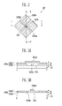
- FIG. 1 is a plan view schematically showing a touch screen panel according to an exemplary embodiment of the present invention.
- FIG. 2 is an enlarged view showing a part of the embodiment of a sensing pattern shown in FIG. 1 .
- FIGS. 3A and 3B are cross sectional views showing cross sections I-I', II-II' of the sensing patterns shown in FIG. 2 .
- FIGS. 4A to 4C are plan views and cross sectional views showing a fabrication process of a touch screen panel according to an exemplary embodiment of the present invention.
- an element when referred to as being “coupled to” (e.g., electrically coupled or connected to) another element, it may be directly coupled to the another element or may be indirectly coupled to the another element with one or more intervening elements interposed therebetween.
- like reference numerals refer to like elements.
- FIG. 1 is a plan view schematically showing a touch screen panel according to an exemplary embodiment of the present invention.
- a touch screen panel may include a transparent base 10, sensing patterns 220 formed in a display region of the transparent base 10, and sensing lines 230 formed in a non-display region and positioned at an outer side of the display region to couple the sensing patterns 220 to an external driving circuit (not shown) via a pad part 250.
- the transparent base 10 may be made of glass, but may also be implemented as a transparent base having a flexible characteristic and may be made of, for example, polyethyleneterephthalate (PET), retardant polycarbonate (PC), cyclic polyolefin (COP), polyimide (PI), polymethylmethacrylate (PMMA), triacetyl cellulose (TAC), ARTON, or the like.
- PET polyethyleneterephthalate
- PC retardant polycarbonate
- COP cyclic polyolefin
- PI polyimide
- PMMA polymethylmethacrylate
- ARTON triacetyl cellulose
- the touch screen panel according to the exemplary embodiment of the present invention as described above is a capacitive type touch screen panel, which when a contact object such as a human hand, a stylus pen, or the like, contacts the touch screen panel, a change in capacitance according to a contact position is transferred from the sensing patterns 220 to the driving circuit (not shown) via the sensing lines 230 and the pad unit 250.
- the change in capacitance may be converted into an electrical signal by an X and Y input processing circuits, or the like (not shown), such that the contact position is recognized.
- the sensing patterns 220 may include first sensing cells 220a and second sensing cells 220b, which may be implemented in a stacked structure.
- Connecting lines coupling the first sensing cells 220a to each other may be formed integrally with an upper layer of the first sensing cells 220a, thereby making it possible to improve visualization of patterns (e.g., reduce observance of the sensing patters 220) and reduce resistance of the connecting lines.
- sensing patterns 220 An embodiment of the sensing patterns 220 according to the present invention will now be described below in detail with reference to FIGS. 2, 3A, and 3B .
- FIG. 2 is an enlarged view showing part of an example sensing pattern shown in FIG. 1
- FIGS. 3A and 3B are cross sectional views showing cross sections I-I', II-II' of the sensing patterns shown in FIG. 2 .
- the sensing patterns 220 include a plurality of first sensing cells 220a formed to be coupled to each other in each row line in a first direction (as an example, an X direction), first connecting lines 220a1 coupling the first sensing cells 220a to each other in the row direction, a plurality of second sensing cells 220b formed to be coupled to each other in each column line in a second direction (as an example, a Y direction), and second connecting lines 220b1 coupling the second cells 220b to each other in the column direction, as shown in FIG. 2 .
- FIG. 2 shows some of the sensing patterns shown in FIG. 1 for convenience
- the touch screen panel has a structure in which the sensing pattern shown in FIG.2 is repeatedly disposed.
- the first and second sensing cells 220a and 220b are alternatively disposed so as not to be overlapped with each other; however, the first and second connecting lines 220a1 and 220b1 overlap with each other.
- the first and second connecting lines 220a1 and 220b1 have an insulating layer 240 interposed therebetween in order to insulate and secure stability (e.g., to provide structural support).
- an island-like insulating layer 240 is formed in order to prevent a short-circuit between the first and second connecting lines 220a1 and 220b1.
- the insulating layer 240 may be an inorganic insulating layer of a transparent material, for example, silicon dioxide (SiO 2 ) or silicon nitride (Si 3 N x ).
- a connecting line may be formed on the insulating layer 240 in a bridge pattern, which may be implemented in a rod shape, in order to couple adjacent sensing cells to each other.
- the bridge pattern having the rod shape may be disposed at a predetermined interval, which may cause a pattern to be viewed by a user, that is, a pattern visualization phenomenon.
- the amount of material used in the bridge pattern and dimensions of length, width, and thickness thereof may be reduced (e.g., be made as small as possible).
- a resistance of the bridge pattern increases, which may cause a deterioration of sensing sensitivity, or the like.
- each of the first and second sensing cells 220a and 220b configuring the sensing pattern 220 may be in a stacked structure comprising an upper layer and a lower layer (see, e.g., in FIGS. 3A and 3B , 220a' and 220a", and 220b' and 220b"), and a first connecting line 220a1 coupling first sensing cells 220a to each other may be formed integrally with upper first sensing cells 220a", which form upper layers of the first sensing cells 220a, thereby preventing (or reducing) visualization (or observation) of a pattern and reducing resistance of the connecting lines.
- the first sensing cell 220a may include a lower first sensing cell 220a' and an upper first sensing cell 220a", which overlaps the lower first sensing cell 220a'.
- the second sensing cell 220b may include a lower second sensing cell 220b' and an upper second sensing cell 220b", which overlaps the lower second sensing cell 220b'.
- the first connecting line 220a1 coupling the first sensing cells 220a to each other may be formed integrally with the upper first sensing cells 220a", which form the upper layers of the adjacent first sensing cells 220a, where the first connecting line 220a1 couples the first sensing cells 220a to each other in a first direction (as an example, a row direction).
- the second connecting line 220b1 coupling the sensing cells 220b to each other may be formed integrally with the lower second sensing cells 220b', which form lower layers of the adjacent second sensing cells 220b, where the second connecting line 220b1 couples the second sensing cells 220b to each other in a second direction (as an example, a column direction).
- the island-like insulating layer 240 may be formed in a region in which the first connecting line 220a and the second connecting line 220b1 overlap each other.
- the sensing cells 220a and 220b having the stacked structure may be made of a transparent conductive material, for example, an indium tin oxide (ITO) material.
- ITO indium tin oxide
- the lower first sensing cells 220a' and the upper first sensing cells 220a" of the first sensing cell 220a, the first connecting lines 220a1 integrally formed with the upper first sensing cell 220a", the lower second sensing cells 220b' and the upper second sensing cells 220b" of the second sensing cell 220b, and the second connecting lines 220b1 integrally formed with the lower second sensing cell 220b' may all be made of the same material.
- the first sensing cells 220a, the second sensing cells 220b, and the connecting lines 220a1 and 220b1 may all made of a crystalline indium tin oxide (poly-ITO).
- the connecting lines having a bridge pattern have been implemented in a rod shape as described above.
- sensing cells positioned beneath the connecting line may also be etched in an etching process for patterning the bridge pattern.
- the connecting line when the connecting line made of the crystalline poly ITO is etched into the bridge pattern, the sensing cell made of the same material as that of the connecting line may also be etched. Therefore, according to the related art, to prevent the above-described etching of the sensing sell, the connecting line may be made of an amorphous indium tin oxide (a-ITO) that has been selectively etched into the bridge pattern separately, and then has been annealed.
- a-ITO amorphous indium tin oxide
- the first connecting line 220a1 formed on the insulating layer 240 may be formed integrally with the upper first sensing cells 220a", which are formed to be overlapped (e.g., completely overlapped) with the lower sensing cells (i.e., the lower first sensing cells 220a'), such that a separate selective-etching need not be performed when the first sensing lines 220a1 and the upper first sensing cells 220a" are patterned.
- the above-described etching phenomena does not occur in the patterning process.
- the same etchant may be used in the process of patterning the sensing cells 220a and 220b and the connecting lines 220a1 and 220b1.
- the same etchant may be used in the process of patterning the sensing cells 220a and 220b and the connecting lines 220a1 and 220b1.
- fewer kinds of etchants than those used in the structure according to the related art may be used, which may reduce confusion in the manufacturing line.
- the first connecting line 220a1 may be formed integrally with the upper first sensing cells 220a", thereby significantly reducing resistance of the connecting line as compared to that in the existing bridge pattern having the rod shape.
- the same (or substantially the same) line resistance as that of the structure according to the related art may be implemented.
- a thickness d1 of the first connecting line 220a1 and the upper first sensing cell 220a" may be smaller than the thickness d2 of the lower first sensing cell 220a'.
- FIGS. 4A to 4C are plan views and cross sectional views showing a fabrication process of a touch screen panel according to the exemplary embodiment of the present invention.
- FIGS. 4A to 4C plan views and cross sectional views shown in FIGS. 4A to 4C will be described with reference to those shown in FIGS. 2 and 3A , by way of example.
- a plurality of lower first sensing cells 220a' arranged on a display region of a transparent base 10 for each line in a first direction (as an example, an X direction or row direction), a plurality of lower second sensing cells 220b' arranged for each line in a second direction (as an example, a Y direction or column direction), and second connecting lines 220b1 coupling the lower second sensing cells 220b' in the column direction.
- the lower first sensing cells 220a' and the lower second sensing cells 220b' may be alternately disposed so as not to be overlapped with each other, as shown in FIG. 4 , and the second connecting lines 220b1 may be formed integrally with the lower second sensing cells 220b' such that adjacent lower second sensing cells 220b' are coupled to each other through the second connecting line 220b1.
- the second connecting line 220b1 may be formed on the same layer, formed of the same transparent conductive material, and formed through the same process as the lower first sensing cells 220a' and the lower second sensing cells 220b'.
- the lower first sensing cells 220a', the lower second sensing cells 220b', and the second connecting lines 220b1 may be made of the transparent conductive material, for example, a crystalline indium tin oxide (poly ITO).
- poly ITO crystalline indium tin oxide
- the insulating layer 240 may be an inorganic insulating layer of a transparent material, for example silicon dioxide (SiO 2 ) or silicon nitride (Si 3 N x ).
- the transparent conductive material 300 may be formed on an entire surface of the transparent base 10 on which the lower first sensing cells 220a', the lower second sensing cells 220b', the second connecting lines 220b1 coupling the lower second sensing cells 220b', and the island-like insulating layer 240 are formed.
- the transparent conductive material may be made of the same material as that of the lower first sensing cells 220a', the lower second sensing cells 220b', and the second connecting lines 220b1, for example, crystalline indium tin oxide (poly ITO).
- poly ITO crystalline indium tin oxide
- the transparent conductive material may be formed of the amorphous indium tin oxide (a-ITO), or the poly-ITO through the annealing process.
- a-ITO amorphous indium tin oxide
- the transparent conductive material 300 may have a thickness smaller than the thickness of the lower first sensing cells 220a', the lower second sensing cells 220b', and the second connecting lines 220b1.
- the transparent conductive material 300 is patterned to form the upper first sensing cells 220a" at the region overlapping with the lower first sensing cells 220a', to from the first connecting lines 220a1 coupling the lower second sensing cells 200a", and to form the upper second sensing cells 220b" at the region overlapping with the lower second sensing cells 220b'.
- the upper first sensing cells 220a" and the upper second sensing cells 220b" are alternately disposed so as not to be overlapped with each other, as shown in FIG. 4 , and the first connecting lines 220a1 are formed integrally with the upper first sensing cells 220a", such that adjacent upper first sensing cells 220a" in the first direction are coupled to each other through the first connecting line 220a1.
- the first connecting line 220a1 may be formed on the same layer, formed of the same transparent conductive material, and formed through the same process as that of the upper first sensing cells 220a" and the upper second sensing cells 220b".
- first connecting line 220a1 and the second connecting line 220b1 overlap each other, they are isolated from each other by the island-like insulating layer 240.
- the first connecting line 220a1 formed on the insulating layer 240 may be formed integrally with the upper first sensing cells 220a", which are formed so as to be overlapped (e.g., completely overlapped) with the lower sensing cells (i.e., the lower first sensing cells 220a'), such that the lower first sensing cells 220a' positioned at a lower portion are overlapped (e.g., completely covered) when the first sensing lines 220a1 and the upper first sensing cells 220a" are patterned. Therefore, the separate selective-etching need not be performed.
- the sensing cells 220a and 220b and the connecting lines 220a1 and 220b1 are all made of the crystalline poly ITO as described above, an etching problem is not generated in the patterning process.
- the same etchant may be used, thereby fewer kinds of etchants than those used in the structure according to the related art may be used and confusion in the manufacturing line may be reduced.
- each of first and second sensing cells 220a and 220b forming the sensing pattern 220 may be implemented in a stacked structure (in the figure, 220a' and 220a", and 220b' and 220b"), and a first connecting line 220a1 coupling first sensing cells to each other may be formed integrally with upper first sensing cells 220a", which form upper layers of the first sensing cells 220a, thereby preventing visualization of the pattern and reducing resistance of the first connecting line 220a1.
- the first and second sensing cells that form the sensing patterns may have a stacked structure, and the connecting line coupling the first sensing cells to each other may be formed integrally with an upper layer of the first sensing cells, thereby improving visualization of patterns and reducing resistance of the connecting line.
Landscapes
- Engineering & Computer Science (AREA)
- General Engineering & Computer Science (AREA)
- Theoretical Computer Science (AREA)
- Human Computer Interaction (AREA)
- Physics & Mathematics (AREA)
- General Physics & Mathematics (AREA)
- Manufacturing & Machinery (AREA)
- Microelectronics & Electronic Packaging (AREA)
- Position Input By Displaying (AREA)
Abstract
Description
- Aspects of the present invention relate to a touch screen panel and a fabrication method thereof.
- A touch screen panel is an input device capable of inputting a user's instruction by selecting instruction contents displayed on a screen of an image display device, or the like, with a human hand or an object.
- To this end, the touch screen panel may be provided on a front surface of the image display device to convert a contact position directly contacted by the human hand or the object into an electric signal. Therefore, the instruction contents selected at the contact position may be recognized as an input signal.
- Since the touch screen panel may be substituted for a separate input device connected to the image display device, such as a keyboard or a mouse, application fields thereof have been gradually extended.
- Example types of the touch screen panel include a resistive type touch screen panel, a photosensitive type touch screen panel, a capacitive type touch screen panel, and the like. Among these, the capacitive type touch screen panel senses a change in capacitance formed between a conductive sensing pattern and neighboring other sensing patterns, a ground electrode, or the like, when a human hand or an object contacts the touch screen panel, thereby converting a contact position into an electric signal.
- The capacitive type touch screen panel may include first sensing cells coupled to each other and formed in a first direction, and second sensing cells coupled to each other and formed in a second direction. Here, adjacent first sensing cells may be electrically connected to each other through a first connecting line, adjacent second sensing cells may be electrically connected to each other through a second connecting line, and the first and second connecting lines may overlap each other (but are insulated by an insulating layer interposed therebetween).
- Particularly, a structure in which the first and second sensing cells are formed on the same layer and the first or second connecting lines are formed on the insulating layer in a bridge pattern to couple the first or second sensing cells to each other, respectively, has been used.
- Here, the connecting lines formed on the insulating layer may be made of the same material as that of the sensing cell, for example, a transparent conductive material (such as, an indium tin oxide (ITO), or a low resistance metal material).
- However, when the above-mentioned structure (that is, the sensing pattern structure in which the connecting lines are included in the bridge pattern) is used, the bridge pattern may be observed (or viewed), which may interfere with an image displayed on the image display device.
- To reduce this interference, the quantity of material used in the bridge pattern and/or dimensions of length, width, and thickness thereof may be reduced (e.g., made as small as possible). However, such a design increases resistance of the bridge pattern, which causes other problems, such as a deterioration of sensing sensitivity and vulnerability to external electrostatic discharge (ESD).
- An aspect of an embodiment according to the present invention is to provide a touch screen panel capable of preventing (or reducing) observation of patterns and reducing resistance of connecting lines by implementing first and second sensing cells, configuring sensing patterns in a stacked structure, and/or forming the connecting lines coupling first sensing cells to each other integrally with an upper layer of the first sensing cells, and a fabrication method thereof.
- Accordingly, an embodiment of the present invention provides a touch screen panel including: sensing patterns in a display region of a transparent base; and sensing lines in a non-display region positioned at an outer side of the display region and coupled to the sensing patterns. Here, the sensing patterns include: a plurality of first sensing cells in a plurality of first lines in a first direction; first connecting lines coupling the first sensing cells in corresponding first lines from among the plurality of first lines to each other; second sensing cells in a plurality of second lines in a second direction; and second connecting lines coupling the second sensing cells in corresponding second lines from among the plurality of second lines to each other, and the first sensing cells and the second sensing cells each have a stacked structure, and the first connecting lines are integral with an upper layer of the first sensing cells.
- Portions of the first connecting lines may overlap portions of the second connecting lines, and an insulating layer may be at a region between the first connecting lines and the second connecting lines.
- Each first sensing cell may include: a lower first sensing cell at a lower portion thereof; and an upper first sensing cell at an upper portion thereof, and each second sensing cell may include: a lower second sensing cell at a lower portion thereof; and an upper second sensing cell at an upper portion thereof.
- In an embodiment of the present invention, the first connecting lines are integral with the upper first sensing cells that are adjacent in the first direction, and the second connecting lines are integral with the upper second sensing cells that are adjacent in the second direction.
- The first connecting lines and the upper first sensing cells may have thicknesses smaller than that of the lower first sensing cells.
- The first sensing cells, the second sensing cells, the first connecting lines, and the second connecting lines may all be made of the same material. In an embodiment of the present invention, the same material is a crystalline indium tin oxide (ITO).
- According to another aspect of the present invention, a method of fabricating a touch screen panel may be provided, the method including: forming a plurality of lower first sensing cells in a display region of a transparent base in a plurality of first lines in a first direction; forming a plurality of lower second sensing cells in the display region of the transparent base in a plurality of second lines in a second direction; forming a plurality of second connecting lines coupling together the lower second sensing cells in corresponding second lines; forming an insulating layer on the second connecting lines; forming a transparent conductive material to cover a region of the transparent base on which the lower first sensing cells, the lower second sensing cells, the second connecting lines, and the insulating layer are formed; and patterning the transparent conductive material to form upper first sensing cells on the lower first sensing cells, to form first connecting lines coupling the upper first sensing cells in corresponding first lines to each other in the first direction, and to form upper second sensing cells on the lower second sensing cells.
- The second connecting lines may be formed integrally with the lower second sensing cells that are adjacent in the second direction, and may be formed of the same material, on the same layer, and through the same process as that of the lower first sensing cells and the lower second sensing cells. In an embodiment of the present invention, the same material is a crystalline indium tin oxide (ITO).
- The transparent conductive material may be made of the same material as that of the lower first sensing cells, the lower second sensing cells, and the second connecting lines.
- The transparent conductive material may have a thickness smaller than thicknesses of the lower first sensing cells, the lower second sensing cells, and the second connecting lines.
- The first connecting lines maybe formed integrally with the upper first sensing cells that are adjacent in the first direction, and may be formed of the same material, on the same layer, and through the same process as that of the upper first sensing cells and the upper second sensing cells.
- The accompanying drawings, together with the specification, illustrate exemplary embodiments of the present invention, and, together with the description, serve to explain aspects of the present invention.
-
FIG. 1 is a plan view schematically showing a touch screen panel according to an exemplary embodiment of the present invention. -
FIG. 2 is an enlarged view showing a part of the embodiment of a sensing pattern shown inFIG. 1 . -
FIGS. 3A and 3B are cross sectional views showing cross sections I-I', II-II' of the sensing patterns shown inFIG. 2 . -
FIGS. 4A to 4C are plan views and cross sectional views showing a fabrication process of a touch screen panel according to an exemplary embodiment of the present invention. - In the following detailed description, only certain exemplary embodiments of the present invention have been shown and described, simply by way of illustration. As those skilled in the art would realize, the described embodiments may be modified in various different ways, all without departing from the scope of the present invention. Accordingly, the drawings and description are to be regarded as illustrative in nature and not restrictive. In addition, when an element is referred to as being "on" another element, it may be directly on the another element or may be indirectly on the another element with one or more intervening elements interposed therebetween. Also, when an element is referred to as being "coupled to" (e.g., electrically coupled or connected to) another element, it may be directly coupled to the another element or may be indirectly coupled to the another element with one or more intervening elements interposed therebetween. Hereinafter, like reference numerals refer to like elements.
- Exemplary embodiments of the present invention will now be described in detail with reference to the accompanying drawings.
-
FIG. 1 is a plan view schematically showing a touch screen panel according to an exemplary embodiment of the present invention. - Referring to
FIG. 1 , a touch screen panel according to an exemplary embodiment of the present invention may include atransparent base 10,sensing patterns 220 formed in a display region of thetransparent base 10, andsensing lines 230 formed in a non-display region and positioned at an outer side of the display region to couple thesensing patterns 220 to an external driving circuit (not shown) via apad part 250. - The
transparent base 10 may be made of glass, but may also be implemented as a transparent base having a flexible characteristic and may be made of, for example, polyethyleneterephthalate (PET), retardant polycarbonate (PC), cyclic polyolefin (COP), polyimide (PI), polymethylmethacrylate (PMMA), triacetyl cellulose (TAC), ARTON, or the like. - The touch screen panel according to the exemplary embodiment of the present invention as described above is a capacitive type touch screen panel, which when a contact object such as a human hand, a stylus pen, or the like, contacts the touch screen panel, a change in capacitance according to a contact position is transferred from the
sensing patterns 220 to the driving circuit (not shown) via thesensing lines 230 and thepad unit 250. In this case, the change in capacitance may be converted into an electrical signal by an X and Y input processing circuits, or the like (not shown), such that the contact position is recognized. - In the exemplary embodiment of the present invention, the
sensing patterns 220 may includefirst sensing cells 220a andsecond sensing cells 220b, which may be implemented in a stacked structure. Connecting lines coupling thefirst sensing cells 220a to each other may be formed integrally with an upper layer of thefirst sensing cells 220a, thereby making it possible to improve visualization of patterns (e.g., reduce observance of the sensing patters 220) and reduce resistance of the connecting lines. - An embodiment of the
sensing patterns 220 according to the present invention will now be described below in detail with reference toFIGS. 2, 3A, and 3B . -
FIG. 2 is an enlarged view showing part of an example sensing pattern shown inFIG. 1 , andFIGS. 3A and 3B are cross sectional views showing cross sections I-I', II-II' of the sensing patterns shown inFIG. 2 . - The
sensing patterns 220 include a plurality offirst sensing cells 220a formed to be coupled to each other in each row line in a first direction (as an example, an X direction), first connecting lines 220a1 coupling thefirst sensing cells 220a to each other in the row direction, a plurality ofsecond sensing cells 220b formed to be coupled to each other in each column line in a second direction (as an example, a Y direction), and second connecting lines 220b1 coupling thesecond cells 220b to each other in the column direction, as shown inFIG. 2 . - Although
FIG. 2 shows some of the sensing patterns shown inFIG. 1 for convenience, the touch screen panel has a structure in which the sensing pattern shown inFIG.2 is repeatedly disposed. - The first and
second sensing cells insulating layer 240 interposed therebetween in order to insulate and secure stability (e.g., to provide structural support). - That is, in a region between the first connecting line 220a1 and the second connecting line 220b1, which overlap with each other, an island-like
insulating layer 240 is formed in order to prevent a short-circuit between the first and second connecting lines 220a1 and 220b1. The insulatinglayer 240 may be an inorganic insulating layer of a transparent material, for example, silicon dioxide (SiO2) or silicon nitride (Si3Nx). - According to the related art, a connecting line may be formed on the insulating
layer 240 in a bridge pattern, which may be implemented in a rod shape, in order to couple adjacent sensing cells to each other. In this case, the bridge pattern having the rod shape may be disposed at a predetermined interval, which may cause a pattern to be viewed by a user, that is, a pattern visualization phenomenon. - In addition, in order to reduce the pattern visualization phenomenon, the amount of material used in the bridge pattern and dimensions of length, width, and thickness thereof may be reduced (e.g., be made as small as possible). However, by reducing the pattern visualization phenomenon in this manner, a resistance of the bridge pattern increases, which may cause a deterioration of sensing sensitivity, or the like.
- Therefore, in an exemplary embodiment of the present invention, each of the first and
second sensing cells sensing pattern 220 may be in a stacked structure comprising an upper layer and a lower layer (see, e.g., inFIGS. 3A and 3B , 220a' and 220a", and 220b' and 220b"), and a first connecting line 220a1 coupling first sensingcells 220a to each other may be formed integrally with upperfirst sensing cells 220a", which form upper layers of thefirst sensing cells 220a, thereby preventing (or reducing) visualization (or observation) of a pattern and reducing resistance of the connecting lines. - That is, the
first sensing cell 220a may include a lowerfirst sensing cell 220a' and an upperfirst sensing cell 220a", which overlaps the lowerfirst sensing cell 220a'. Likewise, thesecond sensing cell 220b may include a lowersecond sensing cell 220b' and an uppersecond sensing cell 220b", which overlaps the lowersecond sensing cell 220b'. - In addition, in the exemplary embodiment of the present invention, the first connecting line 220a1 coupling the
first sensing cells 220a to each other may be formed integrally with the upperfirst sensing cells 220a", which form the upper layers of the adjacentfirst sensing cells 220a, where the first connecting line 220a1 couples thefirst sensing cells 220a to each other in a first direction (as an example, a row direction). Also, the second connecting line 220b1 coupling thesensing cells 220b to each other may be formed integrally with the lowersecond sensing cells 220b', which form lower layers of the adjacentsecond sensing cells 220b, where the second connecting line 220b1 couples thesecond sensing cells 220b to each other in a second direction (as an example, a column direction). - Here, the island-like insulating
layer 240 may be formed in a region in which the first connectingline 220a and the second connecting line 220b1 overlap each other. - In addition, the
sensing cells - Additionally, the lower
first sensing cells 220a' and the upperfirst sensing cells 220a" of thefirst sensing cell 220a, the first connecting lines 220a1 integrally formed with the upperfirst sensing cell 220a", the lowersecond sensing cells 220b' and the uppersecond sensing cells 220b" of thesecond sensing cell 220b, and the second connecting lines 220b1 integrally formed with the lowersecond sensing cell 220b' may all be made of the same material. For example, thefirst sensing cells 220a, thesecond sensing cells 220b, and the connecting lines 220a1 and 220b1 may all made of a crystalline indium tin oxide (poly-ITO). - According to the related art, the connecting lines having a bridge pattern have been implemented in a rod shape as described above. When these connecting lines having a bridge pattern are made of the same material as that of the sensing cells, sensing cells positioned beneath the connecting line may also be etched in an etching process for patterning the bridge pattern.
- For example, in the case in which the sensing cell is made of the crystalline poly ITO, when the connecting line made of the crystalline poly ITO is etched into the bridge pattern, the sensing cell made of the same material as that of the connecting line may also be etched. Therefore, according to the related art, to prevent the above-described etching of the sensing sell, the connecting line may be made of an amorphous indium tin oxide (a-ITO) that has been selectively etched into the bridge pattern separately, and then has been annealed.
- However, in the exemplary embodiment of the invention, instead of implementing the bridge pattern according to the related art, the first connecting line 220a1 formed on the insulating
layer 240 may be formed integrally with the upperfirst sensing cells 220a", which are formed to be overlapped (e.g., completely overlapped) with the lower sensing cells (i.e., the lowerfirst sensing cells 220a'), such that a separate selective-etching need not be performed when the first sensing lines 220a1 and the upperfirst sensing cells 220a" are patterned. - Therefore, in the exemplary embodiment of the present invention, in the case in which the
sensing cells - That is, according to the exemplary embodiment of the present invention, in the process of patterning the
sensing cells - In addition, as shown in
FIGS. 3A and 3B , the first connecting line 220a1 may be formed integrally with the upperfirst sensing cells 220a", thereby significantly reducing resistance of the connecting line as compared to that in the existing bridge pattern having the rod shape. - Therefore, even though the thicknesses of the first and second connecting line 220a1 and the upper
first sensing cells 220a" may be reduced, the same (or substantially the same) line resistance as that of the structure according to the related art may be implemented. - In the exemplary embodiment of the present invention, a thickness d1 of the first connecting line 220a1 and the upper
first sensing cell 220a" may be smaller than the thickness d2 of the lowerfirst sensing cell 220a'. -
FIGS. 4A to 4C are plan views and cross sectional views showing a fabrication process of a touch screen panel according to the exemplary embodiment of the present invention. - Here, plan views and cross sectional views shown in
FIGS. 4A to 4C will be described with reference to those shown inFIGS. 2 and 3A , by way of example. - First, referring to
FIG. 4A , there may be provided a plurality of lowerfirst sensing cells 220a' arranged on a display region of atransparent base 10 for each line in a first direction (as an example, an X direction or row direction), a plurality of lowersecond sensing cells 220b' arranged for each line in a second direction (as an example, a Y direction or column direction), and second connecting lines 220b1 coupling the lowersecond sensing cells 220b' in the column direction. - Here, the lower
first sensing cells 220a' and the lowersecond sensing cells 220b' may be alternately disposed so as not to be overlapped with each other, as shown inFIG. 4 , and the second connecting lines 220b1 may be formed integrally with the lowersecond sensing cells 220b' such that adjacent lowersecond sensing cells 220b' are coupled to each other through the second connecting line 220b1. - That is, the second connecting line 220b1 may be formed on the same layer, formed of the same transparent conductive material, and formed through the same process as the lower
first sensing cells 220a' and the lowersecond sensing cells 220b'. - In addition, the lower
first sensing cells 220a', the lowersecond sensing cells 220b', and the second connecting lines 220b1 may be made of the transparent conductive material, for example, a crystalline indium tin oxide (poly ITO). - Then, as shown in
FIG. 4A , on a region which is overlapped with the second connecting line 220b1, an island-like insulatinglayer 240 may be formed. The insulatinglayer 240 may be an inorganic insulating layer of a transparent material, for example silicon dioxide (SiO2) or silicon nitride (Si3Nx). - Next, referring to
FIG. 4B , the transparentconductive material 300 may be formed on an entire surface of thetransparent base 10 on which the lowerfirst sensing cells 220a', the lowersecond sensing cells 220b', the second connecting lines 220b1 coupling the lowersecond sensing cells 220b', and the island-like insulatinglayer 240 are formed. - Here, the transparent conductive material may be made of the same material as that of the lower
first sensing cells 220a', the lowersecond sensing cells 220b', and the second connecting lines 220b1, for example, crystalline indium tin oxide (poly ITO). - However, at the time of initial deposition of the entire surface, the transparent conductive material may be formed of the amorphous indium tin oxide (a-ITO), or the poly-ITO through the annealing process.
- In addition, in the exemplary embodiment of the present invention, the transparent
conductive material 300 may have a thickness smaller than the thickness of the lowerfirst sensing cells 220a', the lowersecond sensing cells 220b', and the second connecting lines 220b1. - Next, as shown in
FIG. 4C , the transparentconductive material 300 is patterned to form the upperfirst sensing cells 220a" at the region overlapping with the lowerfirst sensing cells 220a', to from the first connecting lines 220a1 coupling the lower second sensing cells 200a", and to form the uppersecond sensing cells 220b" at the region overlapping with the lowersecond sensing cells 220b'. - Here, the upper
first sensing cells 220a" and the uppersecond sensing cells 220b" are alternately disposed so as not to be overlapped with each other, as shown inFIG. 4 , and the first connecting lines 220a1 are formed integrally with the upperfirst sensing cells 220a", such that adjacent upperfirst sensing cells 220a" in the first direction are coupled to each other through the first connecting line 220a1. - That is, the first connecting line 220a1 may be formed on the same layer, formed of the same transparent conductive material, and formed through the same process as that of the upper
first sensing cells 220a" and the uppersecond sensing cells 220b". - Additionally, while the first connecting line 220a1 and the second connecting line 220b1 overlap each other, they are isolated from each other by the island-like insulating
layer 240. - In the exemplary embodiment of the invention, the first connecting line 220a1 formed on the insulating
layer 240 may be formed integrally with the upperfirst sensing cells 220a", which are formed so as to be overlapped (e.g., completely overlapped) with the lower sensing cells (i.e., the lowerfirst sensing cells 220a'), such that the lowerfirst sensing cells 220a' positioned at a lower portion are overlapped (e.g., completely covered) when the first sensing lines 220a1 and the upperfirst sensing cells 220a" are patterned. Therefore, the separate selective-etching need not be performed. - Therefore, in the exemplary embodiment of the present invention, in the case in which the
sensing cells - That is, according to the exemplary embodiment of the present invention, in the process of patterning the
sensing cells - In addition, in the exemplary embodiment of the present invention, each of first and
second sensing cells sensing pattern 220 may be implemented in a stacked structure (in the figure, 220a' and 220a", and 220b' and 220b"), and a first connecting line 220a1 coupling first sensing cells to each other may be formed integrally with upperfirst sensing cells 220a", which form upper layers of thefirst sensing cells 220a, thereby preventing visualization of the pattern and reducing resistance of the first connecting line 220a1. - As set forth above, the first and second sensing cells that form the sensing patterns may have a stacked structure, and the connecting line coupling the first sensing cells to each other may be formed integrally with an upper layer of the first sensing cells, thereby improving visualization of patterns and reducing resistance of the connecting line.
- While the present invention has been described in connection with certain exemplary embodiments, it is to be understood that the invention is not limited to the disclosed embodiments, but, on the contrary, is intended to cover various modifications and equivalent arrangements included within the scope of the appended claims, and equivalents thereof.
Claims (13)
- A touch screen panel comprising:sensing patterns (220) in a display region of a transparent base (10); andsensing lines (230) in a non-display region positioned at an outer side of the display region and coupled to the sensing patterns (200),wherein the sensing patterns (200) comprise:a plurality of first sensing cells (220a) in a plurality of first lines in a first direction;first connecting lines (220a1) coupling the first sensing cells (220a) in corresponding first lines from among the plurality of first lines to each other;a plurality of second sensing cells (220b) in a plurality of second lines in a second direction; andsecond connecting lines (220b1) coupling the second sensing cells (220b) in corresponding second lines from among the plurality of second lines to each other,wherein the first sensing cells (220b) and the second sensing cells (220b) each have a stacked structure, andwherein the first connecting lines (220a1) are integrally formed with an upper layer of the first sensing cells (220a).
- The touch screen panel according to claim 1,
wherein portions of the first connecting lines (220a1) overlap portions of the second connecting lines (220b1), and
wherein an insulating layer (240) is formed at a region between the first connecting lines (220a1) and the second connecting lines (220b1). - The touch screen panel according to one of the preceding claims, wherein each of the first sensing cells (220a) comprises:a lower first sensing cell (220a') at a lower portion thereof; andan upper first sensing cell (220a") at an upper portion thereof, andwherein each of the second sensing cells (220b) comprises:a lower second sensing cell (220b') at a lower portion thereof; andan upper second sensing cell (220b") at an upper portion thereof.
- The touch screen panel according to claim 3,
wherein the first connecting lines (220a1) are integral with the upper first sensing cells (220a") that are adjacent in the first direction, and
wherein the second connecting lines (220b1) are integrally formed with the lower second sensing cells (220b') that are adjacent in the second direction. - The touch screen panel according to claim 4,
wherein the first connecting lines (220a1) and the upper first sensing cells (220a") have thicknesses smaller than that of the lower first sensing cells (220a'). - The touch screen panel according to one of the preceding claims,
wherein the first sensing cells (220a), the second sensing cells (220b), the first connecting lines (220a1), and the second connecting lines (220b1) are all made of the same material. - The touch screen panel according to claim 6,
wherein the same material is a crystalline indium tin oxide (ITO). - A fabrication method of a touch screen panel comprising:forming a plurality of lower first sensing cells (220a') in a display region of a transparent base (10) in a plurality of first lines in a first direction;forming a plurality of lower second sensing cells (220b') in the display region of the transparent base (10) in a plurality of second lines in a second direction;forming a plurality of second connecting lines (220b1) coupling together the lower second sensing cells (220b') in corresponding second lines;forming an insulating layer (240) on portions of the display region that overlap the second connecting lines (220b1);forming a transparent conductive material (300) to cover a region of the transparent base (10) on which the lower first sensing cells (220a'), the lower second sensing cells (220b'), the second connecting lines (220b1), and the insulating layer (240) are formed; andpatterning the transparent conductive material (300) to form upper first sensing cells (220a") on the lower first sensing cells (220a'), to form first connecting lines (220a1) coupling the upper first sensing cells (220a") in corresponding first lines to each other in the first direction, and to form upper second sensing cells (220b") on the lower second sensing cells (220b').
- The fabrication method of a touch screen panel according to claim 8,
wherein the second connecting lines (220b1) are formed integrally with the lower second sensing cells (220b') that are adjacent in the second direction, and are formed of the same material, on the same layer, and through the same process as that of the lower first sensing cells (220a') and the lower second sensing cells (220b'). - The fabrication method of a touch screen panel according to claim 9, wherein the same material is a crystalline indium tin oxide (ITO).
- The fabrication method of a touch screen panel according to one of claims 8 to 10,
wherein the transparent conductive material (300) is made of the same material as that of the lower first sensing cells (220a'), the lower second sensing cells (220b'), and the second connecting lines (220b1). - The fabrication method of a touch screen panel according to one of claims 8 to 11,
wherein the transparent conductive material (300) has a thickness smaller than thicknesses of the lower first sensing cells (220a'), the lower second sensing cells (220b'), and the second connecting lines (220b1). - The fabrication method of a touch screen panel according to one of claims 8 to 12,
wherein the first connecting lines (220a1) are formed integrally with the upper first sensing cells (220a") that are adjacent in the first direction, and are formed of the same material, on the same layer, and through the same process as that of the upper first sensing cells (220a") and the upper second sensing cells (220b").
Applications Claiming Priority (1)
| Application Number | Priority Date | Filing Date | Title |
|---|---|---|---|
| KR1020120080614A KR102012417B1 (en) | 2012-07-24 | 2012-07-24 | Touch Screen Panel and fabrication method thereof |
Publications (3)
| Publication Number | Publication Date |
|---|---|
| EP2690534A2 true EP2690534A2 (en) | 2014-01-29 |
| EP2690534A3 EP2690534A3 (en) | 2015-07-15 |
| EP2690534B1 EP2690534B1 (en) | 2017-08-02 |
Family
ID=47563047
Family Applications (1)
| Application Number | Title | Priority Date | Filing Date |
|---|---|---|---|
| EP12197629.4A Active EP2690534B1 (en) | 2012-07-24 | 2012-12-18 | Touch screen panel and fabrication method thereof |
Country Status (4)
| Country | Link |
|---|---|
| US (1) | US9118329B2 (en) |
| EP (1) | EP2690534B1 (en) |
| KR (1) | KR102012417B1 (en) |
| CN (1) | CN103576972B (en) |
Families Citing this family (7)
| Publication number | Priority date | Publication date | Assignee | Title |
|---|---|---|---|---|
| TWI476659B (en) * | 2012-12-20 | 2015-03-11 | Henghao Technology Co Ltd | Double-layer electrode device |
| US9246485B2 (en) * | 2013-01-11 | 2016-01-26 | Stmicroelectronics Asia Pacific Pte Ltd | Single layer sensor pattern |
| TWI489361B (en) * | 2013-02-08 | 2015-06-21 | Wintek Corp | Touch panel and manufacturing method thereof |
| CN103336602A (en) * | 2013-06-14 | 2013-10-02 | 业成光电(深圳)有限公司 | Touch device |
| KR102192035B1 (en) | 2013-12-02 | 2020-12-17 | 삼성디스플레이 주식회사 | Flexible display device including touch detecting sensor |
| CN103677413B (en) * | 2013-12-09 | 2016-09-21 | 合肥京东方光电科技有限公司 | Touch panel and preparation method thereof, display device |
| TWI564761B (en) * | 2015-01-16 | 2017-01-01 | 友達光電股份有限公司 | Touch electrode layer |
Family Cites Families (9)
| Publication number | Priority date | Publication date | Assignee | Title |
|---|---|---|---|---|
| TW200842681A (en) | 2007-04-27 | 2008-11-01 | Tpk Touch Solutions Inc | Touch pattern structure of a capacitive touch panel |
| KR20100006987A (en) | 2008-07-11 | 2010-01-22 | 삼성모바일디스플레이주식회사 | Touch screen panel and fabricating method for the same |
| WO2010075308A2 (en) * | 2008-12-26 | 2010-07-01 | Atmel Corporation | Multiple electrode touch sensitive device |
| CN102033669B (en) * | 2009-09-24 | 2013-08-14 | 群康科技(深圳)有限公司 | Capacitance-type touch panel |
| US8730184B2 (en) | 2009-12-16 | 2014-05-20 | 3M Innovative Properties Company | Touch sensitive device with multilayer electrode having improved optical and electrical performance |
| KR101101053B1 (en) | 2010-03-16 | 2011-12-29 | 삼성모바일디스플레이주식회사 | Touch Screen Panel and fabrication method thereof |
| KR101323094B1 (en) | 2010-08-25 | 2013-11-04 | 엘지디스플레이 주식회사 | Electrostatic capacitive type touch screen panel and method of manufacturing the same |
| KR101793073B1 (en) * | 2010-12-06 | 2017-11-03 | 삼성디스플레이 주식회사 | Touch Screen Panel |
| TW201234243A (en) * | 2011-02-01 | 2012-08-16 | Ind Tech Res Inst | Projective capacitive touch sensor structure and fabricating method thereof |
-
2012
- 2012-07-24 KR KR1020120080614A patent/KR102012417B1/en active IP Right Grant
- 2012-11-06 US US13/670,425 patent/US9118329B2/en active Active
- 2012-11-22 CN CN201210479219.5A patent/CN103576972B/en active Active
- 2012-12-18 EP EP12197629.4A patent/EP2690534B1/en active Active
Non-Patent Citations (1)
| Title |
|---|
| None |
Also Published As
| Publication number | Publication date |
|---|---|
| US20140027262A1 (en) | 2014-01-30 |
| EP2690534A3 (en) | 2015-07-15 |
| KR102012417B1 (en) | 2019-08-22 |
| US9118329B2 (en) | 2015-08-25 |
| KR20140013483A (en) | 2014-02-05 |
| CN103576972B (en) | 2018-07-20 |
| EP2690534B1 (en) | 2017-08-02 |
| CN103576972A (en) | 2014-02-12 |
Similar Documents
| Publication | Publication Date | Title |
|---|---|---|
| EP2690534B1 (en) | Touch screen panel and fabrication method thereof | |
| US20150085205A1 (en) | Touch panel | |
| US8847906B2 (en) | Touch device and method for manufacturing the same | |
| US10394404B2 (en) | Touch display panel | |
| KR101975535B1 (en) | flexible touch screen panel | |
| KR101410584B1 (en) | Touch panel and a manufacturing method thereof | |
| US8405635B2 (en) | Touch screen panel and fabricating method thereof | |
| US20120182233A1 (en) | Touch screen panel | |
| US9904421B2 (en) | Touch sensor board, image display device, and touch sensor board manufacturing method | |
| KR20160104189A (en) | Touch panel and method for manufacturing the same | |
| KR20140070103A (en) | flexible touch screen panel and fabrication method thereof | |
| CN102799332B (en) | A kind of embedded single layer capacitance touch-screen | |
| US20140152588A1 (en) | Flexible touch screen panel and fabricating method thereof | |
| KR20150139104A (en) | Touch screen panel | |
| CN106155411B (en) | Touch screen, touch panel, display device and electronic equipment | |
| JP5472858B2 (en) | Touch switch | |
| KR200474894Y1 (en) | Double-layer electrode device | |
| US9811230B2 (en) | Touch panel and production method thereof | |
| KR101721259B1 (en) | Electrostatic capacity type touch screen panel and method of manufacturing the same | |
| KR20160060882A (en) | Touch screen panel and method of manufacturing the same | |
| JP6114526B2 (en) | Touch panel | |
| KR102281616B1 (en) | Touch screen panel and method of manufacturing the same | |
| US9323094B2 (en) | Touch panel | |
| JP2016162305A (en) | Touch panel and method for manufacturing the same | |
| US20130008704A1 (en) | Bridging structure of a touch panel |
Legal Events
| Date | Code | Title | Description |
|---|---|---|---|
| PUAI | Public reference made under article 153(3) epc to a published international application that has entered the european phase |
Free format text: ORIGINAL CODE: 0009012 |
|
| AK | Designated contracting states |
Kind code of ref document: A2 Designated state(s): AL AT BE BG CH CY CZ DE DK EE ES FI FR GB GR HR HU IE IS IT LI LT LU LV MC MK MT NL NO PL PT RO RS SE SI SK SM TR |
|
| AX | Request for extension of the european patent |
Extension state: BA ME |
|
| PUAL | Search report despatched |
Free format text: ORIGINAL CODE: 0009013 |
|
| AK | Designated contracting states |
Kind code of ref document: A3 Designated state(s): AL AT BE BG CH CY CZ DE DK EE ES FI FR GB GR HR HU IE IS IT LI LT LU LV MC MK MT NL NO PL PT RO RS SE SI SK SM TR |
|
| AX | Request for extension of the european patent |
Extension state: BA ME |
|
| RIC1 | Information provided on ipc code assigned before grant |
Ipc: G06F 3/044 20060101AFI20150609BHEP |
|
| RAP1 | Party data changed (applicant data changed or rights of an application transferred) |
Owner name: SAMSUNG DISPLAY CO., LTD. |
|
| 17P | Request for examination filed |
Effective date: 20160107 |
|
| RBV | Designated contracting states (corrected) |
Designated state(s): AL AT BE BG CH CY CZ DE DK EE ES FI FR GB GR HR HU IE IS IT LI LT LU LV MC MK MT NL NO PL PT RO RS SE SI SK SM TR |
|
| 17Q | First examination report despatched |
Effective date: 20160208 |
|
| GRAP | Despatch of communication of intention to grant a patent |
Free format text: ORIGINAL CODE: EPIDOSNIGR1 |
|
| INTG | Intention to grant announced |
Effective date: 20170407 |
|
| GRAS | Grant fee paid |
Free format text: ORIGINAL CODE: EPIDOSNIGR3 |
|
| GRAA | (expected) grant |
Free format text: ORIGINAL CODE: 0009210 |
|
| AK | Designated contracting states |
Kind code of ref document: B1 Designated state(s): AL AT BE BG CH CY CZ DE DK EE ES FI FR GB GR HR HU IE IS IT LI LT LU LV MC MK MT NL NO PL PT RO RS SE SI SK SM TR |
|
| REG | Reference to a national code |
Ref country code: CH Ref legal event code: EP Ref country code: AT Ref legal event code: REF Ref document number: 915160 Country of ref document: AT Kind code of ref document: T Effective date: 20170815 |
|
| REG | Reference to a national code |
Ref country code: IE Ref legal event code: FG4D |
|
| REG | Reference to a national code |
Ref country code: DE Ref legal event code: R096 Ref document number: 602012035261 Country of ref document: DE |
|
| REG | Reference to a national code |
Ref country code: NL Ref legal event code: FP |
|
| REG | Reference to a national code |
Ref country code: AT Ref legal event code: MK05 Ref document number: 915160 Country of ref document: AT Kind code of ref document: T Effective date: 20170802 |
|
| REG | Reference to a national code |
Ref country code: LT Ref legal event code: MG4D |
|
| PG25 | Lapsed in a contracting state [announced via postgrant information from national office to epo] |
Ref country code: FI Free format text: LAPSE BECAUSE OF FAILURE TO SUBMIT A TRANSLATION OF THE DESCRIPTION OR TO PAY THE FEE WITHIN THE PRESCRIBED TIME-LIMIT Effective date: 20170802 Ref country code: SE Free format text: LAPSE BECAUSE OF FAILURE TO SUBMIT A TRANSLATION OF THE DESCRIPTION OR TO PAY THE FEE WITHIN THE PRESCRIBED TIME-LIMIT Effective date: 20170802 Ref country code: HR Free format text: LAPSE BECAUSE OF FAILURE TO SUBMIT A TRANSLATION OF THE DESCRIPTION OR TO PAY THE FEE WITHIN THE PRESCRIBED TIME-LIMIT Effective date: 20170802 Ref country code: AT Free format text: LAPSE BECAUSE OF FAILURE TO SUBMIT A TRANSLATION OF THE DESCRIPTION OR TO PAY THE FEE WITHIN THE PRESCRIBED TIME-LIMIT Effective date: 20170802 Ref country code: NO Free format text: LAPSE BECAUSE OF FAILURE TO SUBMIT A TRANSLATION OF THE DESCRIPTION OR TO PAY THE FEE WITHIN THE PRESCRIBED TIME-LIMIT Effective date: 20171102 Ref country code: LT Free format text: LAPSE BECAUSE OF FAILURE TO SUBMIT A TRANSLATION OF THE DESCRIPTION OR TO PAY THE FEE WITHIN THE PRESCRIBED TIME-LIMIT Effective date: 20170802 |
|
| PG25 | Lapsed in a contracting state [announced via postgrant information from national office to epo] |
Ref country code: RS Free format text: LAPSE BECAUSE OF FAILURE TO SUBMIT A TRANSLATION OF THE DESCRIPTION OR TO PAY THE FEE WITHIN THE PRESCRIBED TIME-LIMIT Effective date: 20170802 Ref country code: GR Free format text: LAPSE BECAUSE OF FAILURE TO SUBMIT A TRANSLATION OF THE DESCRIPTION OR TO PAY THE FEE WITHIN THE PRESCRIBED TIME-LIMIT Effective date: 20171103 Ref country code: BG Free format text: LAPSE BECAUSE OF FAILURE TO SUBMIT A TRANSLATION OF THE DESCRIPTION OR TO PAY THE FEE WITHIN THE PRESCRIBED TIME-LIMIT Effective date: 20171102 Ref country code: LV Free format text: LAPSE BECAUSE OF FAILURE TO SUBMIT A TRANSLATION OF THE DESCRIPTION OR TO PAY THE FEE WITHIN THE PRESCRIBED TIME-LIMIT Effective date: 20170802 Ref country code: ES Free format text: LAPSE BECAUSE OF FAILURE TO SUBMIT A TRANSLATION OF THE DESCRIPTION OR TO PAY THE FEE WITHIN THE PRESCRIBED TIME-LIMIT Effective date: 20170802 Ref country code: PL Free format text: LAPSE BECAUSE OF FAILURE TO SUBMIT A TRANSLATION OF THE DESCRIPTION OR TO PAY THE FEE WITHIN THE PRESCRIBED TIME-LIMIT Effective date: 20170802 Ref country code: IS Free format text: LAPSE BECAUSE OF FAILURE TO SUBMIT A TRANSLATION OF THE DESCRIPTION OR TO PAY THE FEE WITHIN THE PRESCRIBED TIME-LIMIT Effective date: 20171202 |
|
| PG25 | Lapsed in a contracting state [announced via postgrant information from national office to epo] |
Ref country code: RO Free format text: LAPSE BECAUSE OF FAILURE TO SUBMIT A TRANSLATION OF THE DESCRIPTION OR TO PAY THE FEE WITHIN THE PRESCRIBED TIME-LIMIT Effective date: 20170802 Ref country code: CZ Free format text: LAPSE BECAUSE OF FAILURE TO SUBMIT A TRANSLATION OF THE DESCRIPTION OR TO PAY THE FEE WITHIN THE PRESCRIBED TIME-LIMIT Effective date: 20170802 Ref country code: DK Free format text: LAPSE BECAUSE OF FAILURE TO SUBMIT A TRANSLATION OF THE DESCRIPTION OR TO PAY THE FEE WITHIN THE PRESCRIBED TIME-LIMIT Effective date: 20170802 |
|
| REG | Reference to a national code |
Ref country code: DE Ref legal event code: R097 Ref document number: 602012035261 Country of ref document: DE |
|
| PG25 | Lapsed in a contracting state [announced via postgrant information from national office to epo] |
Ref country code: SK Free format text: LAPSE BECAUSE OF FAILURE TO SUBMIT A TRANSLATION OF THE DESCRIPTION OR TO PAY THE FEE WITHIN THE PRESCRIBED TIME-LIMIT Effective date: 20170802 Ref country code: EE Free format text: LAPSE BECAUSE OF FAILURE TO SUBMIT A TRANSLATION OF THE DESCRIPTION OR TO PAY THE FEE WITHIN THE PRESCRIBED TIME-LIMIT Effective date: 20170802 Ref country code: IT Free format text: LAPSE BECAUSE OF FAILURE TO SUBMIT A TRANSLATION OF THE DESCRIPTION OR TO PAY THE FEE WITHIN THE PRESCRIBED TIME-LIMIT Effective date: 20170802 Ref country code: SM Free format text: LAPSE BECAUSE OF FAILURE TO SUBMIT A TRANSLATION OF THE DESCRIPTION OR TO PAY THE FEE WITHIN THE PRESCRIBED TIME-LIMIT Effective date: 20170802 |
|
| PLBE | No opposition filed within time limit |
Free format text: ORIGINAL CODE: 0009261 |
|
| STAA | Information on the status of an ep patent application or granted ep patent |
Free format text: STATUS: NO OPPOSITION FILED WITHIN TIME LIMIT |
|
| 26N | No opposition filed |
Effective date: 20180503 |
|
| REG | Reference to a national code |
Ref country code: CH Ref legal event code: PL |
|
| PG25 | Lapsed in a contracting state [announced via postgrant information from national office to epo] |
Ref country code: SI Free format text: LAPSE BECAUSE OF FAILURE TO SUBMIT A TRANSLATION OF THE DESCRIPTION OR TO PAY THE FEE WITHIN THE PRESCRIBED TIME-LIMIT Effective date: 20170802 |
|
| REG | Reference to a national code |
Ref country code: IE Ref legal event code: MM4A |
|
| PG25 | Lapsed in a contracting state [announced via postgrant information from national office to epo] |
Ref country code: LU Free format text: LAPSE BECAUSE OF NON-PAYMENT OF DUE FEES Effective date: 20171218 Ref country code: MT Free format text: LAPSE BECAUSE OF NON-PAYMENT OF DUE FEES Effective date: 20171218 |
|
| REG | Reference to a national code |
Ref country code: FR Ref legal event code: ST Effective date: 20180831 |
|
| REG | Reference to a national code |
Ref country code: BE Ref legal event code: MM Effective date: 20171231 |
|
| PG25 | Lapsed in a contracting state [announced via postgrant information from national office to epo] |
Ref country code: IE Free format text: LAPSE BECAUSE OF NON-PAYMENT OF DUE FEES Effective date: 20171218 Ref country code: FR Free format text: LAPSE BECAUSE OF NON-PAYMENT OF DUE FEES Effective date: 20180102 |
|
| PG25 | Lapsed in a contracting state [announced via postgrant information from national office to epo] |
Ref country code: CH Free format text: LAPSE BECAUSE OF NON-PAYMENT OF DUE FEES Effective date: 20171231 Ref country code: BE Free format text: LAPSE BECAUSE OF NON-PAYMENT OF DUE FEES Effective date: 20171231 Ref country code: LI Free format text: LAPSE BECAUSE OF NON-PAYMENT OF DUE FEES Effective date: 20171231 |
|
| PG25 | Lapsed in a contracting state [announced via postgrant information from national office to epo] |
Ref country code: MC Free format text: LAPSE BECAUSE OF FAILURE TO SUBMIT A TRANSLATION OF THE DESCRIPTION OR TO PAY THE FEE WITHIN THE PRESCRIBED TIME-LIMIT Effective date: 20170802 Ref country code: HU Free format text: LAPSE BECAUSE OF FAILURE TO SUBMIT A TRANSLATION OF THE DESCRIPTION OR TO PAY THE FEE WITHIN THE PRESCRIBED TIME-LIMIT; INVALID AB INITIO Effective date: 20121218 |
|
| PG25 | Lapsed in a contracting state [announced via postgrant information from national office to epo] |
Ref country code: CY Free format text: LAPSE BECAUSE OF NON-PAYMENT OF DUE FEES Effective date: 20170802 |
|
| PG25 | Lapsed in a contracting state [announced via postgrant information from national office to epo] |
Ref country code: MK Free format text: LAPSE BECAUSE OF FAILURE TO SUBMIT A TRANSLATION OF THE DESCRIPTION OR TO PAY THE FEE WITHIN THE PRESCRIBED TIME-LIMIT Effective date: 20170802 |
|
| PG25 | Lapsed in a contracting state [announced via postgrant information from national office to epo] |
Ref country code: TR Free format text: LAPSE BECAUSE OF FAILURE TO SUBMIT A TRANSLATION OF THE DESCRIPTION OR TO PAY THE FEE WITHIN THE PRESCRIBED TIME-LIMIT Effective date: 20170802 |
|
| PG25 | Lapsed in a contracting state [announced via postgrant information from national office to epo] |
Ref country code: PT Free format text: LAPSE BECAUSE OF FAILURE TO SUBMIT A TRANSLATION OF THE DESCRIPTION OR TO PAY THE FEE WITHIN THE PRESCRIBED TIME-LIMIT Effective date: 20170802 |
|
| PG25 | Lapsed in a contracting state [announced via postgrant information from national office to epo] |
Ref country code: AL Free format text: LAPSE BECAUSE OF FAILURE TO SUBMIT A TRANSLATION OF THE DESCRIPTION OR TO PAY THE FEE WITHIN THE PRESCRIBED TIME-LIMIT Effective date: 20170802 |
|
| P01 | Opt-out of the competence of the unified patent court (upc) registered |
Effective date: 20230515 |
|
| PGFP | Annual fee paid to national office [announced via postgrant information from national office to epo] |
Ref country code: NL Payment date: 20231121 Year of fee payment: 12 |
|
| PGFP | Annual fee paid to national office [announced via postgrant information from national office to epo] |
Ref country code: GB Payment date: 20231120 Year of fee payment: 12 |
|
| PGFP | Annual fee paid to national office [announced via postgrant information from national office to epo] |
Ref country code: DE Payment date: 20231120 Year of fee payment: 12 |