EP2688260B1 - Methods and apparatus for adapting transmitter equalization coefficients based on receiver gain adaptation - Google Patents
Methods and apparatus for adapting transmitter equalization coefficients based on receiver gain adaptation Download PDFInfo
- Publication number
- EP2688260B1 EP2688260B1 EP13177107.3A EP13177107A EP2688260B1 EP 2688260 B1 EP2688260 B1 EP 2688260B1 EP 13177107 A EP13177107 A EP 13177107A EP 2688260 B1 EP2688260 B1 EP 2688260B1
- Authority
- EP
- European Patent Office
- Prior art keywords
- receiver
- amplifier
- limit
- transmitter
- gain value
- Prior art date
- Legal status (The legal status is an assumption and is not a legal conclusion. Google has not performed a legal analysis and makes no representation as to the accuracy of the status listed.)
- Active
Links
Images

Classifications
-
- H—ELECTRICITY
- H04—ELECTRIC COMMUNICATION TECHNIQUE
- H04L—TRANSMISSION OF DIGITAL INFORMATION, e.g. TELEGRAPHIC COMMUNICATION
- H04L27/00—Modulated-carrier systems
- H04L27/01—Equalisers
-
- H—ELECTRICITY
- H04—ELECTRIC COMMUNICATION TECHNIQUE
- H04L—TRANSMISSION OF DIGITAL INFORMATION, e.g. TELEGRAPHIC COMMUNICATION
- H04L25/00—Baseband systems
- H04L25/02—Details ; arrangements for supplying electrical power along data transmission lines
- H04L25/03—Shaping networks in transmitter or receiver, e.g. adaptive shaping networks
- H04L25/03006—Arrangements for removing intersymbol interference
- H04L25/03343—Arrangements at the transmitter end
Definitions
- serializer and de-serializer (SerDes) devices facilitate the transmission of parallel data across a serial link.
- Parallel data is converted by the serializer at the transmitter to serial data before transmission through a communications channel to the receiver.
- a de-serializer in the receiver converts the serial data to parallel data.
- Signals arriving at the receiver are typically corrupted by intersymbol interference (ISI), crosstalk, echo and other noise.
- ISI intersymbol interference
- receivers typically amplify and equalize the channel to compensate for such distortions, often using a number of different equalization techniques.
- Decision-feedback equalization DFE
- DFE Decision-feedback equalization
- Equalization may also be employed by the transmitter to pre-condition (e.g., pre-emphasize) the signal prior to transmission.
- Equalization generally requires an estimate of the transfer function of the channel to establish the equalization parameters.
- the frequency-dependent signal degradation characteristics of the communications channel often vary over time or may be not known a priori.
- adaptive equalization is often employed to vary the equalization parameters over time to mitigate the signal degradation.
- the equalization can adaptively respond to changes in channel characteristics or ambient conditions, such as temperature and humidity, and/or adapt from default values to the current channel characteristics.
- Adaptation algorithms typically adapt the filter coefficients in accordance with the signal statistics or the signal spectrum. For example, least mean square (LMS) adaptation techniques are often employed to establish the equalization parameters based on observations of the received signal over time.
- LMS least mean square
- Adaptation of the equalization parameters in the transmitter may adversely impact the gain adjustments and/or equalization performed in the receiver (or vice versa).
- VGA variable gain amplifier
- the equalizer coefficients in the transmitter are often increased towards their upper limits, causing the variable gain amplifier (VGA) in the receiver to likewise settle to its upper limits.
- VGA variable gain amplifier
- the output of the VGA will not follow further increases in emphasis by the transmit equalizer.
- the data eye opening will be smaller and jitter tolerance in the receiver is reduced.
- Embodiments of the present invention can be manifest in adaptive equalization techniques that adjust the transmitter equalization coefficients based on the VGA gain adaptation in the receiver.
- the equalization coefficients in the transmitter e.g., for a TXFIR filter
- the VGA in the receiver may settle to its upper limits.
- the output of the VGA in the receiver will not follow further increases in emphasis by the transmit equalizer.
- the adaptation of the transmitter equalization coefficients is limited such that the equalizer cannot go beyond the abilities of the VGA to amplify the incoming received signal to the required level.
- the VGA gain adaptation is monitored and when the VGA reaches an upper or lower limit, further adjustments of the transmit equalizer coefficients are prevented.
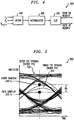
- FIG. 1 is a block diagram of a communication system 100 in which embodiments of the invention may be employed.
- the communication system 100 comprises two SerDes devices 110-1 and 110-2 that communicate over a channel 120.
- the SerDes device 110-1 is operating in a transmit mode and the SerDes device 110-2 is operating in a receive mode.
- adaptation algorithms in the receive SerDes device 110-2 determine one or more adaptive equalization parameters for the transmit SerDes device 110-1, which are communicated from the receive SerDes device 110-2 to the transmit SerDes device 110-1 using a back channel 130.
- serialized transmit data is preconditioned (e.g., pre-emphasized) by a transmit finite impulse response (TXFIR) filter 114 to compensate for impairments caused by the channel 120, in a known manner.
- TXFIR transmit finite impulse response
- the coefficients for the TXFIR filter 114 are determined by adaptation algorithms within a receiver equalization (RXEQ) adaptation block 160 in the receive SerDes device 110-2, as discussed further below in conjunction with equation (1) and FIG. 4 .
- the filtered serial output of the TXFIR filter 114 is applied to the channel 120 and received by the receive SerDes device 110-2.
- the received signal is initially amplified by a Variable Gain Amplifier (VGA) 140, and then enhanced in a receiver front end (RXFE) 142, typically using adjustable high pass filters in order to further mitigate channel impairments.
- VGA Variable Gain Amplifier
- RXFE receiver front end
- the output of RXFE 142 is applied to an adder 144.
- a DFE correction from a decision-feedback equalizer (DFE) 150 is applied to the adder 144 in a feedback fashion to produce a DFE corrected signal 141.
- the DFE correction compensates for Inter Symbol Interference (ISI) occurring in the channel 120.
- ISI Inter Symbol Interference
- the DFE corrected signal 141 is then sampled by slicers 146.
- the slicers 146 typically sample the serial data one or more times for each serial bit duration Unit Interval (UI) in order to recover the serial data and bit clock.
- the sampled serial data from the slicers 146 is then deserialized by deserializer 148.
- the recovered data from deserializer 148 is processed in a feedback loop by the DFE 150 to generate the DFE correction.
- the recovery of the bit clock and other timing issues are well-known to those of ordinary skill in the art.
- the recovered data from deserializer 148 is also processed by one or more adaptation algorithms within the RXEQ adaptation block 160 in the receive SerDes device 110-2 to determine equalization parameters for the VGA 140, RXFE 142 and DFE 150.
- the adaptation is performed using recovered data and error information through the RXEQ Adaptation block 160.
- the adaptation algorithm within the RXEQ adaptation block 160 may be implemented, for example, as the well-known LMS or Zero Forcing (ZF) algorithms. Exemplary adaptation algorithms are discussed further below in the section entitled "Exemplary Adaptation Algorithms.”
- the VGA 140 receives a gain control signal from the RXEQ adaptation block 160.
- the RXFE 142 and DFE 150 receive filter coefficients from the RXEQ adaptation block 160.
- the filter coefficient adjustments for the TXFIR filter 114 in the transmit SerDes device 110-1 are also determined by the RXEQ adaptation block 160.
- the RXEQ adaptation block 160 can employ the LMS algorithm to produce TXFIR UP or DN (down) adjustment requests for different TXFIR coefficients.
- the TXFIR UP or DN adjustment requests generated by the RXEQ adaptation block 160 change the amount of emphasis for main cursor, pre-cursors and post-cursors in the TXFIR filter 114, thus training the remote transmit SerDes device 110-1 to the conditions of the particular channel 120.
- Pre-cursor and post cursor TXFIR coefficients are normally negative values to create pre-emphasis.
- a DN adjustment request indicates an increase in the amount of pre-emphasis
- an UP adjustment request indicates a decrease in the amount of pre-emphasis.
- the RXEQ adaptation block 160 applies the determined TXFIR coefficient adjustments to link logic 165, which in turn applies the coefficient adjustment requests to the transmit (TX) portion 170 of the receive SerDes device 110-2.
- the TX portion 170 of the receive SerDes device 110-2 transmits UP or DN (down) requests for the coefficients over the back channel 130 to the receive (RX) portion 116 of the SerDes device 110-1.
- Link logic 118 applies the received filter UP or DN requests for coefficients to the TXFIR filter 114 thus changing the amount of pre-emphasis or the main cursor value.
- the present invention is described in the context of the communication system 100 having two SerDes devices 110-1 and 110-2, the present invention can apply to any communication system having serial communications from a transmitter to a receiver and where equalization updates can be provided from the receiver to the transmitter, as would be apparent to a person of ordinary skill in the art.
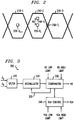
- FIG. 2 illustrates a sampling of a series of data eyes 210-1 through 210-3 corresponding to the DFE corrected signal 141 by slicers 146.
- the slicers 146 of FIG. 1 comprise two data slicers 220-D i and 220-D i-1 , transition slicer 230-T i , and error slicer 240-E i .
- the transition slicer 230-T i is aligned with the statistical middle of the data transitions crossing level "0," data slicer 220-D i is aligned to the statistical center of the data eye with a vertical (voltage) offset of zero, and the error slicer 240-E i has the same timing alignment as data slicer 220-D i but with a vertical offset of H0, typically positioning the error slicer 240-E i in the statistical middle of the data levels at the center of the eye (statistical middle between inner and outer data eyes), as discussed further below in conjunction with FIG. 5 .
- the H0 vertical offset is achieved as a part of VGA adaptation, and the error slicer 240-E i is used in the LMS adaptation algorithm of all RXEQ parameters, as well as remote TXFIR coefficients, in a known manner. There may be one or more error slicers 240-E i per data eye.
- Equation (1) if the current data sample D k from data slicer 220-D k has the same sign as the error offset Esign k , then an exclusive NOR ("XNOR") operation is applied to the data sample offset by the coefficient index n, D k-n , and the current error sample, E k , from error slicer 240-E k , and accumulated as an UP or DOWN adjustment into the coefficient value.
- XNOR exclusive NOR
- the adaptation algorithm for the coefficients for the remote TXFIR filter 114 can also be described by equation (1) with a corresponding +1 or -1 index offset n for pre-cursor and post cursor adaptation.
- H 0 D k ⁇ Esign k ⁇ ? ⁇ 0 ⁇ D k ⁇ E k ⁇ : 0
- equation (2) if the current data sample D k from data slicer 220-D k has the same sign as the error offset Esign k , then an exclusive NOR "XNOR" operation is applied to the current data sample D k and the current error sample, E k , from error slicer 240-E k , and accumulated as an UP or DOWN adjustment into the error slicer offset value.
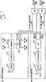
- FIG. 3 is a block diagram illustrating a VGA/H0 adaptation block 300, based on equation (2).
- the current data sample D k from data slicer 220-D k and the current error sample, E k , from error slicer 240-E k are applied to an UP/DN decision block 310 described by equation (2), and then an accumulator 320 accumulates the values by adding or subtracting, respectively, from the current level of H0.
- a comparator 330 receives upper and lower limits for H0 which are typically narrower than the full range of H0 control. The range between H0 limits is related to one step of VGA control, and should be greater than this step.
- H0 accumulator Whenever the comparator 330 determines that H0 control reaches an upper or lower H0 limit, the H0 accumulator is reset to its restart level (between lower and upper limits) using feedback path 335 and VGA Control 340 is incremented or decremented by one. For example, if H0 adaptation causes its accumulator 320 to reach a lower limit, then the signal from the channel 120 is not strong enough, and the signal should get a higher amplification (by increasing the gain adjustment signal applied to VGA 140). In this case, the VGA gain adjustment signal (control) is incremented by one.
- the algorithm shown in FIG. 3 runs until H0 settles at a steady level between the corresponding lower and upper limits or the VGA control 340 reaches a predefined low or high limit (all limits are typically programmable). In the latter case, the VGA control 340 stops at the low limit or high limit correspondingly, and H0 is allowed to accumulate beyond its preset limits anywhere within the available range. In this case, VGA amplification may not be enough, and the vertical eye opening may suffer, leading to inferior jitter tolerance. Conversely, if VGA control 340 reaches the lower limit, this may mean that the signal cannot be attenuated enough, and may suffer saturation through the RXFE 142, which is typically not as critical as the lack of amplification, but may cause undesirable non linear effects.
- FIG. 4 is a block diagram illustrating a TXFIR filter coefficient adaptation block 400 for the remote TXFIR filter 114 based on equation (1).
- the current data sample D k from data slicer 220-D k and the current error sample, E k , from error slicer 240-E k , as well as the prior or subsequent data sample D k+/-1 from the corresponding data slicer 220 are applied to an UP/DN decision block 410 described by equation (1), and then an accumulator 420 accumulates the values by adding or subtracting, respectively, from the current accumulator 420 values.
- the clip block 430 latches the value and the value is conveyed to the link logic 165 as UP or DN requests to be sent through the back channel 130 to the remote SerDes 110-1. In this manner, the TXFIR coefficient values are adjusted to the parameters of the communications channel 120.
- FIG. 5 illustrates a data eye diagram 500 overlaid with data slicer 220-D i and error slicer 240-E i .
- the data eye has an inner eye opening 510, also referred to as the inner eye 510, which is the minimum opening where no traces are going through.
- the data eye has an outer eye opening 520, also referred to as the outer eye 520, which is the maximum of the data eye.
- the data slicer 220-D i is aligned to the statistical center of the data eye with a vertical (voltage) offset of zero, and the error slicer 240-E i has the same timing alignment as data slicer 220-D i but with a vertical offset of H0, typically positioning the error slicer 240-E i in the statistical middle of the data levels at the center of the eye (statistical middle between inner eye 510 and outer eye 520).
- equalization aims to open the size of the data eye (i.e., increase the data margin). Nonetheless, it has been found that equalization can increase the inner eye 510 by an amount that is smaller than the amount that the outer eye 520 decreases (e.g., outer eye 520 closes more than the inner eye 510 opens). This will cause the statistical middle between the inner eye 510 and the outer eye 520 to reduce, and the offset level H0 for the error latch 240-E i will readapt to a lower value. The reduction to the H0 level can in turn cause an increase in the VGA gain adjustment, as discussed above in conjunction with FIG. 3 .
- the TXFIR filter 114 typically has a limited bandwidth and acts as a low pass filter. Thus, lower frequency components in the serial data will not suffer the same degradation as pre-emphasis levels.
- adaptation of the equalization parameters in a transmit SerDes 110-1 may adversely impact the gain adjustments and/or equalization performed in a receive SerDes 110-2 (or vice versa).
- the coefficients for the TXFIR 114 in the transmit SerDes 110-1 are often increased towards their upper negative limits, causing the VGA 140 in the receive SerDes 110-2 to likewise settle to its upper limits.
- the output of the VGA 140 will not follow further increases in emphasis by the TXFIR filter 114.
- the data eye opening will be smaller and the jitter tolerance in the receiver is reduced.
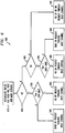
- FIG. 6 is a flow chart describing a limited TXFIR adaptation process 600 embodiment of the present invention.
- the limited TXFIR adaptation process 600 may be implemented, for example, by the RXEQ adaptation block 160.
- the limited TXFIR adaptation process 600 prevents the TXFIR 114 from going beyond the abilities of the VGA 140 to amplify the incoming RX signal to the required level.
- the limited TXFIR adaptation process 600 initially accumulates UP/DN adjustment requests for the pre, post and main cursors of the TXFIR filter 114 during step 610.
- a test is performed during step 620 to determine if the request is an UP request (reduction in pre-emphasis causing a reduction in inner eye 510 and an increase in outer eye 520). If it is determined during step 620 that the request is an UP request (for example, a binary value of 01), then a further test is performed during step 630 to determine if the VGA 140 is already at its lower limit.
- step 630 If it is determined during step 630 that the VGA 140 is already at its lower limit, then the UP request is suppressed at step 650 and is not sent over the back channel 140. If, however, it is determined during step 630 that the VGA 140 is not at its lower limit, then the UP request is allowed to be sent over the back channel 140 during step 640.
- step 620 If, however, it was determined during step 620 that the request is not an UP request, then a further test is performed during step 660 to determine if the request is a DN request (for example, a binary value of 11 or 2's complement of -1), then a further test is performed during step 670 to determine if the VGA 140 is already at its high limit. If it is determined during step 670 that the VGA 140 is already at its high limit, then the DN request (increase in pre-emphasis) is suppressed at step 680 and is not sent over the back channel 140. If, however, it is determined during step 670 that the VGA 140 is not at its high limit, then the DN request is allowed to be sent over the back channel 140 during step 690.
- a DN request for example, a binary value of 11 or 2's complement of -1
- a request is not sent through the back channel 140 during step 695.
- FIG. 7 is a block diagram of a limited TXFIR adaptation system 700 embodiment of the present invention.
- the limited TXFIR adaptation system 700 comprises the VGA/H0 adaptation block 300 of FIG. 3 and the TXFIR adaptation block 400 of FIG. 4 .
- the VGA/H0 adaptation block 300 of FIG. 3 has been modified to generate two flags 705-H and 705-L indicating when the VGA high and low limits, respectively, have been reached.
- the limited TXFIR adaptation system 700 includes request gating blocks 710, 720 that gate the UP/DN requests, respectively.
- the request gating block 710 receives the UP requests from the TXFIR adaptation block 400, as well as the VGA flag 705-L indicating whether the VGA 140 has reached its lower limit.
- the VGA low limit flag 705-L serves as a disable signal for the request gating block 710.
- the request gating block 710 will allow the UP requests to pass to the back channel 140 as long as the VGA 140 is above low limit.
- the request gating block 720 receives the DN requests from the TXFIR adaptation block 400, as well as the VGA flag 705-H indicating whether the VGA 140 has reached its upper limit.
- the VGA upper limit flag 705-H serves as a disable signal for the request gating block 720.
- the request gating block 720 will allow the DN requests to pass to the back channel 140 as long as the VGA 140 is below low limit.
- the disclosed exemplary improved adaptive equalization techniques adjust the TXFIR coefficients based on the VGA gain adaptation and do not establish TXFIR coefficients that are beyond the limits of the VGA.
- At least a portion of the techniques of the present invention may be implemented in one or more ICs.
- die are typically fabricated in a repeated pattern on a surface of a semiconductor wafer.
- Each of the die includes a stripline device described herein, and may include other structures or circuits.
- Individual die are cut or diced from the wafer, then packaged as integrated circuits.
- One skilled in the art would know how to dice wafers and package die to produce integrated circuits. Integrated circuits so manufactured are considered part of this invention.
- An IC in accordance with the present invention can be employed in many application and/or electronic systems. Suitable systems for implementing the invention may include, but are not limited to, communication devices and devices for distributing cable television signals and other high speed signals. Systems incorporating such integrated circuits are considered part of this invention. Given the teachings of the invention provided herein, one of ordinary skill in the art will be able to contemplate other implementations and applications of the techniques of the invention.
- the integrated circuit design can be created in a graphical computer programming language, and can be stored in a computer storage medium (such as a disk, tape, physical hard drive, or virtual hard drive such as in a storage access network).
- the stored design can be converted into the appropriate format (e.g., Graphic Design System II (GDSII)) for the fabrication of photolithographic masks, which typically include multiple copies of the integrated circuit design that are formed on a wafer.
- GDSII Graphic Design System II
- the photolithographic masks are utilized to define areas of the wafer (and/or the layers thereon) to be etched or otherwise processed.
- the resulting integrated circuits may be distributed by the fabricator in raw wafer form (i.e., as a single wafer that has multiple unpackaged integrated circuits), as a bare die, or in packaged form.
- the integrated circuit is mounted in a single integrated circuit package (e.g., plastic carrier with leads that are affixed to a motherboard or other higher level carrier) or in a multi-integrated circuit package (e.g., ceramic carrier that has either or both surface interconnections or buried interconnections).
- the integrated circuit can be integrated with other chips, discrete circuit elements, and/or other signal processing devices as part of either an intermediate product (e.g., motherboard) or an end product.
- the end product may be any product that includes integrated circuits.
Landscapes
- Engineering & Computer Science (AREA)
- Computer Networks & Wireless Communication (AREA)
- Signal Processing (AREA)
- Power Engineering (AREA)
- Dc Digital Transmission (AREA)
- Cable Transmission Systems, Equalization Of Radio And Reduction Of Echo (AREA)
Applications Claiming Priority (1)
| Application Number | Priority Date | Filing Date | Title |
|---|---|---|---|
| US13/552,012 US9385897B2 (en) | 2012-07-18 | 2012-07-18 | Methods and apparatus for adapting transmitter equalization coefficients based on receiver gain adaptation |
Publications (3)
| Publication Number | Publication Date |
|---|---|
| EP2688260A2 EP2688260A2 (en) | 2014-01-22 |
| EP2688260A3 EP2688260A3 (en) | 2015-10-07 |
| EP2688260B1 true EP2688260B1 (en) | 2017-05-31 |
Family
ID=49035264
Family Applications (1)
| Application Number | Title | Priority Date | Filing Date |
|---|---|---|---|
| EP13177107.3A Active EP2688260B1 (en) | 2012-07-18 | 2013-07-18 | Methods and apparatus for adapting transmitter equalization coefficients based on receiver gain adaptation |
Country Status (6)
Families Citing this family (12)
| Publication number | Priority date | Publication date | Assignee | Title |
|---|---|---|---|---|
| US9503717B2 (en) | 2012-01-09 | 2016-11-22 | Texas Instruments Incorporated | Context adaptive binary arithmetic coding (CABAC) with scalable throughput and coding efficiency |
| US8848769B2 (en) * | 2012-10-09 | 2014-09-30 | Lsi Corporation | Joint transmitter and receiver gain optimization for high-speed serial data systems |
| US9197458B1 (en) * | 2014-05-01 | 2015-11-24 | Samsung Display Co., Ltd. | Edge equalization via adjustment of unroll threshold for crossing slicer |
| TWI597610B (zh) * | 2014-05-07 | 2017-09-01 | 円星科技股份有限公司 | 基於接收單元之等化器的資訊而收發訊號的方法以及訓練等化器的方法 |
| TWI574512B (zh) * | 2015-09-03 | 2017-03-11 | 威盛電子股份有限公司 | 切分器裝置及其校準方法 |
| US9866412B2 (en) * | 2016-01-29 | 2018-01-09 | Samsung Display Co., Ltd. | Equalization in high speed links through in-situ channel estimation |
| CN107241160B (zh) * | 2016-03-28 | 2021-03-23 | 华为技术有限公司 | 确定参数的方法和装置 |
| CN106953818B (zh) * | 2017-02-10 | 2020-10-20 | 张家港康得新光电材料有限公司 | 均衡器设置装置 |
| US10153917B1 (en) * | 2017-07-21 | 2018-12-11 | Huawei Technologies Co., Ltd. | Frequency/phase-shift-keying for back-channel serdes communication |
| CN107508618B (zh) * | 2017-08-29 | 2021-03-19 | 苏州裕太微电子有限公司 | 一种基于有线通信的抗信号衰减的方法及通信设备 |
| CN112117606A (zh) * | 2019-06-21 | 2020-12-22 | 默升科技集团有限公司 | 具有预设预均衡的有源以太网电缆 |
| US11463284B1 (en) * | 2021-07-09 | 2022-10-04 | Cadence Design Systems, Inc. | Programmable correlation computation system |
Family Cites Families (15)
| Publication number | Priority date | Publication date | Assignee | Title |
|---|---|---|---|---|
| US5678198A (en) | 1991-05-22 | 1997-10-14 | Southwestern Bell Technology Resources, Inc. | System for controlling signal level at both ends of a transmission link, based upon a detected value |
| US5991311A (en) * | 1997-10-25 | 1999-11-23 | Centillium Technology | Time-multiplexed transmission on digital-subscriber lines synchronized to existing TCM-ISDN for reduced cross-talk |
| US6141634A (en) * | 1997-11-26 | 2000-10-31 | International Business Machines Corporation | AC power line network simulator |
| DE10141597B4 (de) * | 2001-08-24 | 2017-11-09 | Lantiq Deutschland Gmbh | Verfahren zum Rekonstruieren von über eine Übertragungsstrecke übertragenen Daten in einem Empfänger und entsprechende Vorrichtung |
| US7589927B2 (en) * | 2005-08-30 | 2009-09-15 | International Business Machines Corporation | Dynamically adapting a read channel equalizer |
| US8428111B2 (en) * | 2006-05-23 | 2013-04-23 | Broadcom Corporation | Crosstalk emission management |
| US7711043B2 (en) | 2006-09-29 | 2010-05-04 | Agere Systems Inc. | Method and apparatus for determining latch position for decision-feedback equalization using single-sided eye |
| US20090097538A1 (en) | 2007-10-10 | 2009-04-16 | Aziz Pervez M | Methods And Apparatus For Adaptive Equalization Using Pattern Detection Methods |
| JP5126364B2 (ja) * | 2008-08-05 | 2013-01-23 | 富士通株式会社 | 送信装置および調整値測定方法 |
| US8848774B2 (en) | 2008-08-19 | 2014-09-30 | Lsi Corporation | Adaptation of a linear equalizer using a virtual decision feedback equalizer (VDFE) |
| US8135100B2 (en) | 2008-08-20 | 2012-03-13 | International Business Machines Corporation | Adaptive clock and equalization control systems and methods for data receivers in communications systems |
| US8472513B2 (en) | 2009-01-14 | 2013-06-25 | Lsi Corporation | TX back channel adaptation algorithm |
| US8229020B2 (en) | 2009-03-23 | 2012-07-24 | Oracle America, Inc. | Integrated equalization and CDR adaptation engine with single error monitor circuit |
| US8432955B2 (en) * | 2009-07-10 | 2013-04-30 | Futurewei Technologies, Inc. | Method for robust crosstalk precoder training in channels with impulse noise |
| US8432960B2 (en) | 2010-03-18 | 2013-04-30 | Freescale Semiconductor, Inc. | Digital adaptive channel equalizer |
-
2012
- 2012-07-18 US US13/552,012 patent/US9385897B2/en active Active
-
2013
- 2013-07-17 TW TW102125628A patent/TW201406085A/zh unknown
- 2013-07-17 KR KR1020130084345A patent/KR20140011286A/ko not_active Withdrawn
- 2013-07-17 JP JP2013148220A patent/JP2014023156A/ja not_active Withdrawn
- 2013-07-18 CN CN201310381433.1A patent/CN103581079B/zh active Active
- 2013-07-18 EP EP13177107.3A patent/EP2688260B1/en active Active
Also Published As
| Publication number | Publication date |
|---|---|
| JP2014023156A (ja) | 2014-02-03 |
| EP2688260A3 (en) | 2015-10-07 |
| TW201406085A (zh) | 2014-02-01 |
| KR20140011286A (ko) | 2014-01-28 |
| US20140023131A1 (en) | 2014-01-23 |
| CN103581079B (zh) | 2018-06-22 |
| EP2688260A2 (en) | 2014-01-22 |
| US9385897B2 (en) | 2016-07-05 |
| CN103581079A (zh) | 2014-02-12 |
Similar Documents
| Publication | Publication Date | Title |
|---|---|---|
| EP2688260B1 (en) | Methods and apparatus for adapting transmitter equalization coefficients based on receiver gain adaptation | |
| US11115247B2 (en) | Methods and circuits for asymmetric distribution of channel equalization between devices | |
| US20230291617A1 (en) | Edge based partial response equalization | |
| US8737549B2 (en) | Receiver having limiter-enhanced data eye openings | |
| US9705708B1 (en) | Integrated circuit with continuously adaptive equalization circuitry | |
| US7623600B2 (en) | High speed receive equalizer architecture | |
| EP2119156B1 (en) | Adaptive continuous-time equalizer for correcting the first post-cursor isi | |
| US8705672B2 (en) | Method of compensating for nonlinearity in a DFE-based receiver | |
| US9025655B1 (en) | Transmitter training using receiver equalizer coefficients | |
| US8116364B2 (en) | Selective slicing equalizer | |
| US9917709B2 (en) | DeSerializer DC offset adaptation based on decision feedback equalizer adaptation | |
| US20150256364A1 (en) | Group delay based back channel post cursor adaptation | |
| US20050254569A1 (en) | System and method for generating equalization coefficients | |
| US20240388474A1 (en) | Dynamic In-Situ Adaptation of Data Interface | |
| EP2075930A1 (en) | Methods and apparatus for improved jitter tolerance in an SFP limit amplified signal | |
| CN120582936A (zh) | 基于符号-符号最小均方算法的决策回授均衡器 |
Legal Events
| Date | Code | Title | Description |
|---|---|---|---|
| PUAI | Public reference made under article 153(3) epc to a published international application that has entered the european phase |
Free format text: ORIGINAL CODE: 0009012 |
|
| AK | Designated contracting states |
Kind code of ref document: A2 Designated state(s): AL AT BE BG CH CY CZ DE DK EE ES FI FR GB GR HR HU IE IS IT LI LT LU LV MC MK MT NL NO PL PT RO RS SE SI SK SM TR |
|
| AX | Request for extension of the european patent |
Extension state: BA ME |
|
| PUAL | Search report despatched |
Free format text: ORIGINAL CODE: 0009013 |
|
| AK | Designated contracting states |
Kind code of ref document: A3 Designated state(s): AL AT BE BG CH CY CZ DE DK EE ES FI FR GB GR HR HU IE IS IT LI LT LU LV MC MK MT NL NO PL PT RO RS SE SI SK SM TR |
|
| AX | Request for extension of the european patent |
Extension state: BA ME |
|
| RIC1 | Information provided on ipc code assigned before grant |
Ipc: H04L 25/03 20060101AFI20150901BHEP |
|
| 17P | Request for examination filed |
Effective date: 20160406 |
|
| RBV | Designated contracting states (corrected) |
Designated state(s): AL AT BE BG CH CY CZ DE DK EE ES FI FR GB GR HR HU IE IS IT LI LT LU LV MC MK MT NL NO PL PT RO RS SE SI SK SM TR |
|
| GRAP | Despatch of communication of intention to grant a patent |
Free format text: ORIGINAL CODE: EPIDOSNIGR1 |
|
| STAA | Information on the status of an ep patent application or granted ep patent |
Free format text: STATUS: GRANT OF PATENT IS INTENDED |
|
| INTG | Intention to grant announced |
Effective date: 20161213 |
|
| GRAS | Grant fee paid |
Free format text: ORIGINAL CODE: EPIDOSNIGR3 |
|
| GRAA | (expected) grant |
Free format text: ORIGINAL CODE: 0009210 |
|
| STAA | Information on the status of an ep patent application or granted ep patent |
Free format text: STATUS: THE PATENT HAS BEEN GRANTED |
|
| AK | Designated contracting states |
Kind code of ref document: B1 Designated state(s): AL AT BE BG CH CY CZ DE DK EE ES FI FR GB GR HR HU IE IS IT LI LT LU LV MC MK MT NL NO PL PT RO RS SE SI SK SM TR |
|
| REG | Reference to a national code |
Ref country code: CH Ref legal event code: EP Ref country code: GB Ref legal event code: FG4D |
|
| REG | Reference to a national code |
Ref country code: AT Ref legal event code: REF Ref document number: 898353 Country of ref document: AT Kind code of ref document: T Effective date: 20170615 |
|
| REG | Reference to a national code |
Ref country code: IE Ref legal event code: FG4D |
|
| REG | Reference to a national code |
Ref country code: DE Ref legal event code: R096 Ref document number: 602013021627 Country of ref document: DE |
|
| REG | Reference to a national code |
Ref country code: NL Ref legal event code: FP |
|
| REG | Reference to a national code |
Ref country code: LT Ref legal event code: MG4D |
|
| REG | Reference to a national code |
Ref country code: AT Ref legal event code: MK05 Ref document number: 898353 Country of ref document: AT Kind code of ref document: T Effective date: 20170531 |
|
| PG25 | Lapsed in a contracting state [announced via postgrant information from national office to epo] |
Ref country code: LT Free format text: LAPSE BECAUSE OF FAILURE TO SUBMIT A TRANSLATION OF THE DESCRIPTION OR TO PAY THE FEE WITHIN THE PRESCRIBED TIME-LIMIT Effective date: 20170531 Ref country code: FI Free format text: LAPSE BECAUSE OF FAILURE TO SUBMIT A TRANSLATION OF THE DESCRIPTION OR TO PAY THE FEE WITHIN THE PRESCRIBED TIME-LIMIT Effective date: 20170531 Ref country code: GR Free format text: LAPSE BECAUSE OF FAILURE TO SUBMIT A TRANSLATION OF THE DESCRIPTION OR TO PAY THE FEE WITHIN THE PRESCRIBED TIME-LIMIT Effective date: 20170901 Ref country code: HR Free format text: LAPSE BECAUSE OF FAILURE TO SUBMIT A TRANSLATION OF THE DESCRIPTION OR TO PAY THE FEE WITHIN THE PRESCRIBED TIME-LIMIT Effective date: 20170531 Ref country code: NO Free format text: LAPSE BECAUSE OF FAILURE TO SUBMIT A TRANSLATION OF THE DESCRIPTION OR TO PAY THE FEE WITHIN THE PRESCRIBED TIME-LIMIT Effective date: 20170831 Ref country code: ES Free format text: LAPSE BECAUSE OF FAILURE TO SUBMIT A TRANSLATION OF THE DESCRIPTION OR TO PAY THE FEE WITHIN THE PRESCRIBED TIME-LIMIT Effective date: 20170531 Ref country code: AT Free format text: LAPSE BECAUSE OF FAILURE TO SUBMIT A TRANSLATION OF THE DESCRIPTION OR TO PAY THE FEE WITHIN THE PRESCRIBED TIME-LIMIT Effective date: 20170531 |
|
| PG25 | Lapsed in a contracting state [announced via postgrant information from national office to epo] |
Ref country code: BG Free format text: LAPSE BECAUSE OF FAILURE TO SUBMIT A TRANSLATION OF THE DESCRIPTION OR TO PAY THE FEE WITHIN THE PRESCRIBED TIME-LIMIT Effective date: 20170831 Ref country code: SE Free format text: LAPSE BECAUSE OF FAILURE TO SUBMIT A TRANSLATION OF THE DESCRIPTION OR TO PAY THE FEE WITHIN THE PRESCRIBED TIME-LIMIT Effective date: 20170531 Ref country code: RS Free format text: LAPSE BECAUSE OF FAILURE TO SUBMIT A TRANSLATION OF THE DESCRIPTION OR TO PAY THE FEE WITHIN THE PRESCRIBED TIME-LIMIT Effective date: 20170531 Ref country code: LV Free format text: LAPSE BECAUSE OF FAILURE TO SUBMIT A TRANSLATION OF THE DESCRIPTION OR TO PAY THE FEE WITHIN THE PRESCRIBED TIME-LIMIT Effective date: 20170531 Ref country code: IS Free format text: LAPSE BECAUSE OF FAILURE TO SUBMIT A TRANSLATION OF THE DESCRIPTION OR TO PAY THE FEE WITHIN THE PRESCRIBED TIME-LIMIT Effective date: 20170930 |
|
| PG25 | Lapsed in a contracting state [announced via postgrant information from national office to epo] |
Ref country code: RO Free format text: LAPSE BECAUSE OF FAILURE TO SUBMIT A TRANSLATION OF THE DESCRIPTION OR TO PAY THE FEE WITHIN THE PRESCRIBED TIME-LIMIT Effective date: 20170531 Ref country code: DK Free format text: LAPSE BECAUSE OF FAILURE TO SUBMIT A TRANSLATION OF THE DESCRIPTION OR TO PAY THE FEE WITHIN THE PRESCRIBED TIME-LIMIT Effective date: 20170531 Ref country code: EE Free format text: LAPSE BECAUSE OF FAILURE TO SUBMIT A TRANSLATION OF THE DESCRIPTION OR TO PAY THE FEE WITHIN THE PRESCRIBED TIME-LIMIT Effective date: 20170531 Ref country code: CZ Free format text: LAPSE BECAUSE OF FAILURE TO SUBMIT A TRANSLATION OF THE DESCRIPTION OR TO PAY THE FEE WITHIN THE PRESCRIBED TIME-LIMIT Effective date: 20170531 Ref country code: SK Free format text: LAPSE BECAUSE OF FAILURE TO SUBMIT A TRANSLATION OF THE DESCRIPTION OR TO PAY THE FEE WITHIN THE PRESCRIBED TIME-LIMIT Effective date: 20170531 |
|
| PG25 | Lapsed in a contracting state [announced via postgrant information from national office to epo] |
Ref country code: SM Free format text: LAPSE BECAUSE OF FAILURE TO SUBMIT A TRANSLATION OF THE DESCRIPTION OR TO PAY THE FEE WITHIN THE PRESCRIBED TIME-LIMIT Effective date: 20170531 Ref country code: PL Free format text: LAPSE BECAUSE OF FAILURE TO SUBMIT A TRANSLATION OF THE DESCRIPTION OR TO PAY THE FEE WITHIN THE PRESCRIBED TIME-LIMIT Effective date: 20170531 Ref country code: IT Free format text: LAPSE BECAUSE OF FAILURE TO SUBMIT A TRANSLATION OF THE DESCRIPTION OR TO PAY THE FEE WITHIN THE PRESCRIBED TIME-LIMIT Effective date: 20170531 |
|
| REG | Reference to a national code |
Ref country code: CH Ref legal event code: PL |
|
| REG | Reference to a national code |
Ref country code: DE Ref legal event code: R097 Ref document number: 602013021627 Country of ref document: DE |
|
| PLBE | No opposition filed within time limit |
Free format text: ORIGINAL CODE: 0009261 |
|
| STAA | Information on the status of an ep patent application or granted ep patent |
Free format text: STATUS: NO OPPOSITION FILED WITHIN TIME LIMIT |
|
| REG | Reference to a national code |
Ref country code: IE Ref legal event code: MM4A |
|
| GBPC | Gb: european patent ceased through non-payment of renewal fee |
Effective date: 20170831 |
|
| REG | Reference to a national code |
Ref country code: FR Ref legal event code: ST Effective date: 20180330 |
|
| PG25 | Lapsed in a contracting state [announced via postgrant information from national office to epo] |
Ref country code: LI Free format text: LAPSE BECAUSE OF NON-PAYMENT OF DUE FEES Effective date: 20170731 Ref country code: IE Free format text: LAPSE BECAUSE OF NON-PAYMENT OF DUE FEES Effective date: 20170718 Ref country code: CH Free format text: LAPSE BECAUSE OF NON-PAYMENT OF DUE FEES Effective date: 20170731 |
|
| 26N | No opposition filed |
Effective date: 20180301 |
|
| PG25 | Lapsed in a contracting state [announced via postgrant information from national office to epo] |
Ref country code: FR Free format text: LAPSE BECAUSE OF NON-PAYMENT OF DUE FEES Effective date: 20170731 Ref country code: SI Free format text: LAPSE BECAUSE OF FAILURE TO SUBMIT A TRANSLATION OF THE DESCRIPTION OR TO PAY THE FEE WITHIN THE PRESCRIBED TIME-LIMIT Effective date: 20170531 |
|
| REG | Reference to a national code |
Ref country code: BE Ref legal event code: MM Effective date: 20170731 |
|
| PG25 | Lapsed in a contracting state [announced via postgrant information from national office to epo] |
Ref country code: LU Free format text: LAPSE BECAUSE OF NON-PAYMENT OF DUE FEES Effective date: 20170718 |
|
| PG25 | Lapsed in a contracting state [announced via postgrant information from national office to epo] |
Ref country code: GB Free format text: LAPSE BECAUSE OF NON-PAYMENT OF DUE FEES Effective date: 20170831 |
|
| PG25 | Lapsed in a contracting state [announced via postgrant information from national office to epo] |
Ref country code: BE Free format text: LAPSE BECAUSE OF NON-PAYMENT OF DUE FEES Effective date: 20170731 |
|
| REG | Reference to a national code |
Ref country code: DE Ref legal event code: R082 Ref document number: 602013021627 Country of ref document: DE Representative=s name: DILG, HAEUSLER, SCHINDELMANN PATENTANWALTSGESE, DE Ref country code: DE Ref legal event code: R081 Ref document number: 602013021627 Country of ref document: DE Owner name: BROADCOM INTERNATIONAL PTE. LTD., SG Free format text: FORMER OWNER: LSI CORPORATION, SAN JOSE, CALIF., US Ref country code: DE Ref legal event code: R082 Ref document number: 602013021627 Country of ref document: DE Representative=s name: DILG HAEUSLER SCHINDELMANN PATENTANWALTSGESELL, DE Ref country code: DE Ref legal event code: R081 Ref document number: 602013021627 Country of ref document: DE Owner name: AVAGO TECHNOLOGIES GENERAL IP (SINGAPORE) PTE., SG Free format text: FORMER OWNER: LSI CORPORATION, SAN JOSE, CALIF., US Ref country code: DE Ref legal event code: R081 Ref document number: 602013021627 Country of ref document: DE Owner name: AVAGO TECHNOLOGIES INTERNATIONAL SALES PTE. LT, SG Free format text: FORMER OWNER: LSI CORPORATION, SAN JOSE, CALIF., US |
|
| PG25 | Lapsed in a contracting state [announced via postgrant information from national office to epo] |
Ref country code: MT Free format text: LAPSE BECAUSE OF NON-PAYMENT OF DUE FEES Effective date: 20170718 |
|
| REG | Reference to a national code |
Ref country code: DE Ref legal event code: R081 Ref document number: 602013021627 Country of ref document: DE Owner name: AVAGO TECHNOLOGIES INTERNATIONAL SALES PTE. LI, SG Free format text: FORMER OWNER: AVAGO TECHNOLOGIES GENERAL IP (SINGAPORE) PTE. LTD., SINGAPORE, SG Ref country code: DE Ref legal event code: R081 Ref document number: 602013021627 Country of ref document: DE Owner name: AVAGO TECHNOLOGIES INTERNATIONAL SALES PTE. LT, SG Free format text: FORMER OWNER: AVAGO TECHNOLOGIES GENERAL IP (SINGAPORE) PTE. LTD., SINGAPORE, SG Ref country code: DE Ref legal event code: R082 Ref document number: 602013021627 Country of ref document: DE Representative=s name: DILG, HAEUSLER, SCHINDELMANN PATENTANWALTSGESE, DE Ref country code: DE Ref legal event code: R081 Ref document number: 602013021627 Country of ref document: DE Owner name: BROADCOM INTERNATIONAL PTE. LTD., SG Free format text: FORMER OWNER: AVAGO TECHNOLOGIES GENERAL IP (SINGAPORE) PTE. LTD., SINGAPORE, SG Ref country code: DE Ref legal event code: R082 Ref document number: 602013021627 Country of ref document: DE Representative=s name: DILG HAEUSLER SCHINDELMANN PATENTANWALTSGESELL, DE |
|
| PG25 | Lapsed in a contracting state [announced via postgrant information from national office to epo] |
Ref country code: HU Free format text: LAPSE BECAUSE OF FAILURE TO SUBMIT A TRANSLATION OF THE DESCRIPTION OR TO PAY THE FEE WITHIN THE PRESCRIBED TIME-LIMIT; INVALID AB INITIO Effective date: 20130718 Ref country code: MC Free format text: LAPSE BECAUSE OF FAILURE TO SUBMIT A TRANSLATION OF THE DESCRIPTION OR TO PAY THE FEE WITHIN THE PRESCRIBED TIME-LIMIT Effective date: 20170531 |
|
| PG25 | Lapsed in a contracting state [announced via postgrant information from national office to epo] |
Ref country code: CY Free format text: LAPSE BECAUSE OF NON-PAYMENT OF DUE FEES Effective date: 20170531 |
|
| PG25 | Lapsed in a contracting state [announced via postgrant information from national office to epo] |
Ref country code: MK Free format text: LAPSE BECAUSE OF FAILURE TO SUBMIT A TRANSLATION OF THE DESCRIPTION OR TO PAY THE FEE WITHIN THE PRESCRIBED TIME-LIMIT Effective date: 20170531 |
|
| PG25 | Lapsed in a contracting state [announced via postgrant information from national office to epo] |
Ref country code: TR Free format text: LAPSE BECAUSE OF FAILURE TO SUBMIT A TRANSLATION OF THE DESCRIPTION OR TO PAY THE FEE WITHIN THE PRESCRIBED TIME-LIMIT Effective date: 20170531 |
|
| PG25 | Lapsed in a contracting state [announced via postgrant information from national office to epo] |
Ref country code: PT Free format text: LAPSE BECAUSE OF FAILURE TO SUBMIT A TRANSLATION OF THE DESCRIPTION OR TO PAY THE FEE WITHIN THE PRESCRIBED TIME-LIMIT Effective date: 20170531 |
|
| PG25 | Lapsed in a contracting state [announced via postgrant information from national office to epo] |
Ref country code: AL Free format text: LAPSE BECAUSE OF FAILURE TO SUBMIT A TRANSLATION OF THE DESCRIPTION OR TO PAY THE FEE WITHIN THE PRESCRIBED TIME-LIMIT Effective date: 20170531 |
|
| REG | Reference to a national code |
Ref country code: DE Ref legal event code: R081 Ref document number: 602013021627 Country of ref document: DE Owner name: AVAGO TECHNOLOGIES INTERNATIONAL SALES PTE. LI, SG Free format text: FORMER OWNER: AVAGO TECHNOLOGIES INTERNATIONAL SALES PTE. LTD., SINGAPUR, SG Ref country code: DE Ref legal event code: R082 Ref document number: 602013021627 Country of ref document: DE Representative=s name: DILG, HAEUSLER, SCHINDELMANN PATENTANWALTSGESE, DE Ref country code: DE Ref legal event code: R081 Ref document number: 602013021627 Country of ref document: DE Owner name: BROADCOM INTERNATIONAL PTE. LTD., SG Free format text: FORMER OWNER: AVAGO TECHNOLOGIES INTERNATIONAL SALES PTE. LTD., SINGAPUR, SG |
|
| REG | Reference to a national code |
Ref country code: NL Ref legal event code: PD Owner name: BROADCOM INTERNATIONAL PTE. LTD.; SG Free format text: DETAILS ASSIGNMENT: CHANGE OF OWNER(S), ASSIGNMENT; FORMER OWNER NAME: LSI CORPORATION Effective date: 20201126 |
|
| REG | Reference to a national code |
Ref country code: DE Ref legal event code: R081 Ref document number: 602013021627 Country of ref document: DE Owner name: AVAGO TECHNOLOGIES INTERNATIONAL SALES PTE. LI, SG Free format text: FORMER OWNER: BROADCOM INTERNATIONAL PTE. LTD., SINGAPUR, SG |
|
| REG | Reference to a national code |
Ref country code: NL Ref legal event code: PD Owner name: AVAGO TECHNOLOGIES INTERNATIONAL SALES PTE. LIMITED; SG Free format text: DETAILS ASSIGNMENT: CHANGE OF OWNER(S), MERGE; FORMER OWNER NAME: LSI CORPORATION Effective date: 20230315 |
|
| PGFP | Annual fee paid to national office [announced via postgrant information from national office to epo] |
Ref country code: DE Payment date: 20240710 Year of fee payment: 12 |
|
| PGFP | Annual fee paid to national office [announced via postgrant information from national office to epo] |
Ref country code: NL Payment date: 20250620 Year of fee payment: 13 |