EP2687963A2 - Display device having touch sensing function - Google Patents
Display device having touch sensing function Download PDFInfo
- Publication number
- EP2687963A2 EP2687963A2 EP13152963.8A EP13152963A EP2687963A2 EP 2687963 A2 EP2687963 A2 EP 2687963A2 EP 13152963 A EP13152963 A EP 13152963A EP 2687963 A2 EP2687963 A2 EP 2687963A2
- Authority
- EP
- European Patent Office
- Prior art keywords
- substrate
- coils
- display device
- group
- emr
- Prior art date
- Legal status (The legal status is an assumption and is not a legal conclusion. Google has not performed a legal analysis and makes no representation as to the accuracy of the status listed.)
- Withdrawn
Links
Images



Classifications
-
- G—PHYSICS
- G06—COMPUTING OR CALCULATING; COUNTING
- G06F—ELECTRIC DIGITAL DATA PROCESSING
- G06F3/00—Input arrangements for transferring data to be processed into a form capable of being handled by the computer; Output arrangements for transferring data from processing unit to output unit, e.g. interface arrangements
- G06F3/01—Input arrangements or combined input and output arrangements for interaction between user and computer
- G06F3/03—Arrangements for converting the position or the displacement of a member into a coded form
- G06F3/041—Digitisers, e.g. for touch screens or touch pads, characterised by the transducing means
- G06F3/044—Digitisers, e.g. for touch screens or touch pads, characterised by the transducing means by capacitive means
- G06F3/0446—Digitisers, e.g. for touch screens or touch pads, characterised by the transducing means by capacitive means using a grid-like structure of electrodes in at least two directions, e.g. using row and column electrodes
-
- G—PHYSICS
- G06—COMPUTING OR CALCULATING; COUNTING
- G06F—ELECTRIC DIGITAL DATA PROCESSING
- G06F3/00—Input arrangements for transferring data to be processed into a form capable of being handled by the computer; Output arrangements for transferring data from processing unit to output unit, e.g. interface arrangements
- G06F3/01—Input arrangements or combined input and output arrangements for interaction between user and computer
- G06F3/03—Arrangements for converting the position or the displacement of a member into a coded form
- G06F3/041—Digitisers, e.g. for touch screens or touch pads, characterised by the transducing means
- G06F3/046—Digitisers, e.g. for touch screens or touch pads, characterised by the transducing means by electromagnetic means
-
- G—PHYSICS
- G06—COMPUTING OR CALCULATING; COUNTING
- G06F—ELECTRIC DIGITAL DATA PROCESSING
- G06F3/00—Input arrangements for transferring data to be processed into a form capable of being handled by the computer; Output arrangements for transferring data from processing unit to output unit, e.g. interface arrangements
- G06F3/01—Input arrangements or combined input and output arrangements for interaction between user and computer
- G06F3/03—Arrangements for converting the position or the displacement of a member into a coded form
- G06F3/041—Digitisers, e.g. for touch screens or touch pads, characterised by the transducing means
-
- G—PHYSICS
- G06—COMPUTING OR CALCULATING; COUNTING
- G06F—ELECTRIC DIGITAL DATA PROCESSING
- G06F3/00—Input arrangements for transferring data to be processed into a form capable of being handled by the computer; Output arrangements for transferring data from processing unit to output unit, e.g. interface arrangements
- G06F3/01—Input arrangements or combined input and output arrangements for interaction between user and computer
- G06F3/03—Arrangements for converting the position or the displacement of a member into a coded form
- G06F3/041—Digitisers, e.g. for touch screens or touch pads, characterised by the transducing means
- G06F3/0416—Control or interface arrangements specially adapted for digitisers
- G06F3/04164—Connections between sensors and controllers, e.g. routing lines between electrodes and connection pads
-
- G—PHYSICS
- G06—COMPUTING OR CALCULATING; COUNTING
- G06F—ELECTRIC DIGITAL DATA PROCESSING
- G06F2203/00—Indexing scheme relating to G06F3/00 - G06F3/048
- G06F2203/041—Indexing scheme relating to G06F3/041 - G06F3/045
- G06F2203/04106—Multi-sensing digitiser, i.e. digitiser using at least two different sensing technologies simultaneously or alternatively, e.g. for detecting pen and finger, for saving power or for improving position detection
Definitions
- Embodiments of the present invention relate to a display device capable of sensing touch.
- Touch screen panels are used as input units of smart phones and smart pads, which are currently widely used.
- a touch screen panel is an input device capable of enabling the selection of information or content displayed on a screen of a display device by using a user's finger to input the user's command. Therefore, the touch screen panel is provided on a front face of the display device to convert a contact position of the user's finger into an electrical signal. Therefore, the instruction contact selected by the contact position is received as an input signal.
- the touch screen panel may replace other input devices coupled to the image display device, such as a keyboard and a mouse, the use range thereof is increasing.
- Methods of realizing a touch screen panel include a resistance layer method, a photo-sensing method, and an electro-capacitive method.
- the electro-capacitive touch screen panel is widely used, and detects change in capacitance between conductive sensing patterns and other peripheral sensing patterns or a ground electrode when the finger contacts the touch screen panel, thereby converting the contact position into the electrical signal.
- the electro-capacitive touch screen panel is commonly attached to the external surface of a display device, such as a liquid crystal display (LCD) and an organic light emitting display (OLED).
- a display device such as a liquid crystal display (LCD) and an organic light emitting display (OLED).
- LCD liquid crystal display
- OLED organic light emitting display
- a display device driving integrated circuit (IC) and a touch screen panel driving IC are additionally provided, products are not easily compatible with each other. Since the display device driving IC and the touch screen panel driving IC are coupled to separate flexible printed circuit boards (FPCB), respectively, manufacturing processes are complicated and product cost increases.
- FPCB flexible printed circuit boards
- a pen applied to the conventional electro-capacitive touch screen panel generates a specific signal by internal battery power supply, and the sensing electrodes of the touch screen panel sense the signal.
- the size of the pen increases, and the battery must be changed periodically.
- embodiments of the present invention provide a display device in which an electromagnetic resonance (EMR) sensor unit for sensing the contact of a stylus pen is formed on one surface of a substrate to reduce or minimize the thickness of the display device and to sense a touch more precisely.
- EMR electromagnetic resonance
- Embodiments of the present invention also provide a display device in which the EMR sensor unit and the display device are coupled to a single flexible printed circuit board (FPCB) to simplify manufacturing processes and to reduce product cost.
- Embodiments of the present invention also provide a display device whose top substrate is used as the substrate of a touch screen panel to reduce or minimize the thickness of the display device, and to improve visibility of an image.
- a display device including a plurality of pixels at a display region of a first substrate, and an electromagnetic resonance (EMR) sensor unit at one surface of the first substrate, the EMR sensor unit including a first group of coils and a second group of coils, the first group of coils and the second group of coils being laminated, wherein the EMR sensor unit is beneath the plurality of pixels.
- EMR electromagnetic resonance
- the EMR sensor unit may further include an insulating layer on a front face of the first group of coils, and a planarized buffer layer on the second group of coils, the first group of coils may be directly on one surface of the first substrate, and the second group of coils may be on the insulating layer and may be arranged in a direction that crosses the first group of coils.
- the plurality of pixels may be at the buffer layer.
- the EMR sensor unit may be wider than the display region of the first substrate.
- the first group of coils and the second groups of coils may include first coils and second coils arranged in a first direction and a second direction, respectively, and the first and second coils may include first terminals coupled to a ground power supply, and second terminals coupled to an EMR pad unit coupled to an EMR IC.
- the first coils and the second coils may include a patterned low resistance colored metal.
- the display device may further include a shield layer at a bottom surface of the first substrate.
- the first substrate may be transparent and may include a glass substrate or a material having a flexible characteristic.
- the first substrate may include polyimide.
- a display device having a touch sensing function, the display device including a plurality of pixels at a display region of a first substrate, signal lines coupled to the plurality of pixels and located at a non-display region at an outline of the display region of the first substrate, an EMR sensor unit between a top surface of the first substrate and a bottom surface of the plurality of pixels, the EMR sensor unit including a first group of coils and a second group of coils, the first group of coils and the second group of coils being laminated, a driving pad unit electrically coupled to the signal lines and located at one end of the non-display region, and an EMR pad unit at a same surface as the driving pad unit to be adjacent the driving pad unit and electrically coupled to the EMR sensor unit.
- the driving pad unit and the EMR pad unit may be electrically coupled to a flexible printed circuit board (FPCB).
- FPCB flexible printed circuit board
- the EMR sensor unit may further include an insulating layer on a front surface of the first group of coils, and a planarizing buffer layer on the second group of coils, and the first group of coils may be directly on one surface of the first substrate, and the second group of coils may be on the insulating layer and arranged in a direction that crosses the first group of coils.
- the first group of coils and the second group of coils may include first coils and second coils arranged in a first direction and a second direction, respectively, and the first coils and the second coils may include first terminals coupled to a ground power supply, and second terminals coupled to the EMR pad unit coupled to an EMR IC.
- First lines and second lines extending from the first group of coils and the second group of coils may be electrically coupled to pads of the EMR pad unit through a contact hole.
- a display device having a touch sensing function, the display device including a plurality of pixels at a display region of a first substrate, signal lines coupled to the plurality of pixels and located at a non-display region at an outline of the display region of the first substrate, an EMR sensor unit between a top surface of the first substrate and a bottom surface of the plurality of pixels, and including a first group of coils and a second group of coils, the first group of coils and the second group of coils being laminated, a second substrate on the first substrate to seal the first substrate, the second substrate having a display region and a non-display region at the outline of the display region of the second substrate, a plurality of sensing patterns at the display region of the second substrate, a plurality of sensing lines coupled to sensing patterns and located at the non-display region of the second substrate, and a sealing material at an edge of the non-display region of the second substrate to couple the first substrate and the second substrate to each other.
- the display device may further include a first touch pad unit at the non-display region of the second substrate and overlapping the sealing material to be electrically coupled to a plurality of sensing lines.
- the display device may further include a driving pad unit at one end of the non-display region of the first substrate to be electrically coupled to the signal lines, an EMR pad unit at a same surface as, and next to, the driving pad unit, and electrically coupled to the EMR sensor unit, and a second touch pad unit at the same surface as, and next to, the driving pad unit, and electrically coupled to the first touch pad unit.
- a plurality of pads of the first touch pad unit may be electrically coupled to pads of the second touch pad unit through a plurality of conductive media in the sealing material.
- the driving pad unit, the EMR pad unit, and the second touch pad unit may be electrically coupled to a flexible printed circuit board (FPCB).
- FPCB flexible printed circuit board
- the EMR sensor unit may further include an insulting layer on a front face of the first group of coils, and a planarized buffer layer on the second group of coils, and the first group of coils may be directly on one surface of the first substrate, and the second group of coils may be on the insulating layer and may be arranged in a direction that crosses the first group of coils.
- the first group of coils and the second group of coils may include first coils and second coils arranged in a first direction and a second direction, respectively, and the first coils and the second coils may include first terminals coupled to a ground power supply, and second terminals coupled to an EMR pad unit coupled to an EMR IC.
- First lines and second lines extending from the first group of coils and the second group of coils may be electrically coupled to pads of the EMR pad unit through a contact hole.
- the sensing patterns may include first sensing cells coupled by row line in a first direction, first coupling lines for coupling the first sensing cells in the first direction, second sensing cells coupled by column line in a second direction, and second coupling lines for coupling the second sensing cells in the second direction.
- the sensing patterns may be at a same layer.
- the second sensing cells may be integrated with the second coupling lines.
- the display device may further include an insulating layer at crossing regions of the first coupling lines and the second coupling lines.
- the sensing patterns are at an internal surface of the second substrate that faces the first substrate.
- the EMR sensor unit for sensing contact of the stylus pen is formed on one surface of the substrate of the display device to reduce or minimize the thickness of the display device, and to sense a touch more precisely.
- the EMR sensor unit and the display device are coupled to one FPCB so that it is possible to simplify manufacturing processes and to reduce product cost.
- the top substrate of the display device may also be used as the substrate of the touch screen panel.
- the touch screen panel and the EMR sensor unit are mounted on the top and bottom of the display device, respectively. Therefore, it is possible to reduce or minimize the thickness of the display device, to improve visibility of an image, and to sense a touch more precisely.
- an electromagnetic resonance (EMR) sensor unit is formed on one surface of the bottom substrate of a display device, and an electro-capacitive touch screen panel is formed on one surface of the top substrate of the display device, so that the entire thickness of the display device may be reduced or minimized, and so that contact or touch by a passive stylus pen (e.g., a stylus pen having no battery) and/or a finger may be sensed.
- EMR electromagnetic resonance
- the display device may be, for example, a liquid crystal display (LCD) or an organic light emitting display (OLED). Since the OLED may have a flexible characteristic, the OLED may be used as the display device according to the present embodiment. Therefore, in describing the present embodiment, the OLED is taken as an example.
- LCD liquid crystal display
- OLED organic light emitting display
- FIG. 1 is an exploded plan view of a display device according to the present embodiment of the present invention.
- FIGS. 2A and 2B are sectional views illustrating a coupling type of the pad units of the embodiment illustrated in FIG. 1 .
- the present embodiment is applied to an OLED in which a touch screen panel and an EMR sensor unit are integrated with each other. Sensing patterns and sensing lines for realizing the touch screen panel are directly formed on one surface of the top substrate 200 of the OLED, and a first group of coils and a second group of coils that are part of the EMR sensor unit are directly formed on one surface of the bottom substrate 100 of the OLED.
- the top substrate 200 that functions as the encapsulating substrate of the OLED may be formed of, for example, a glass material or a thin film having a flexible characteristic.
- one surface of the top substrate 200 may be the internal surface of the top substrate. Therefore, one surface of the top substrate illustrated in FIG. 1 corresponds to the internal surface of the top substrate.
- sensing patterns 220 of the touch screen panel may be formed on the external surface of the top substrate 200, and/or may be formed on the internal and external surfaces of the top substrate.
- the EMR sensor unit is mounted on the bottom substrate 100.
- a passive stylus pen including a resonance circuit contacts the display device, coils in the EMR sensor unit adjacent the contact position form a magnetic field.
- the EMR sensor unit senses the resonance frequency of the resonance circuit, the resonance frequency being generated by the resonance circuit resonating with the magnetic field, to determine the contact position.
- sensing patterns 220 of a touch screen panel, and sensing lines 230 for coupling the sensing patterns 220 to an external touch integrated circuit (IC) (not shown) through a first touch pad unit 119a are formed on one surface of a top substrate 200 that seals a bottom substrate 100 with respect to a plurality of pixels 112 formed in a display region 500 of the bottom substrate 100.
- an EMR sensor unit (not shown) realized by a lamination structure of a first group of coils (not shown) and a second group of coils (not shown) is formed on one surface of the bottom substrate 100 where the plurality of pixels 112 are formed. That is, the EMR sensor unit is directly formed on one surface of the bottom substrate 100, and the plurality of pixels 112 are formed on a region that overlaps the EMR sensor unit.
- the sensing patterns 220 are formed on the display region 500 of the top substrate 200, the sensing lines 230 are formed on a non-display region 510 positioned on the outline of the display region 500, and a sealing material 400 for attaching the top substrate 200 to the bottom substrate 100 is coated at the edge of the non-display region 510.
- a plurality of signal lines 114 and 116 are coupled to the pixels 112 formed on the display region 500 of the bottom substrate 100, and the signal lines 114 and 116 are arranged on the non-display region 510.
- scan lines 114 and data lines 116 are arranged as the signal lines.
- emission control lines for controlling emission of organic light emitting diodes (OLED) provided in pixels may also be provided.
- the pixels include OLEDs that are self-emissive elements, a plurality of transistors, and at least one capacitor.
- the signal lines 114 and 116 are coupled to a driving pad unit 118 provided at one end of the non-display region 510 of the bottom substrate 100 to receive signals from an external driving IC (not shown) mounted on a flexible printed circuit board (FPCB) 300.
- FPCB flexible printed circuit board
- a second touch pad unit 119b and an EMR pad unit 120 are adjacently located on side surfaces of the driving pad unit 118, respectively.
- the EMR sensor unit is electrically coupled to the EMR pad unit 120.
- the first touch pad unit 119a formed on the top substrate 200 is electrically coupled to the second touch pad unit 119b.
- Coupling of the first touch pad unit 119a formed on the top substrate 200 to the second touch pad unit 119b formed on the bottom substrate 100 may be realized by the present embodiment illustrated in FIG. 2A . That is, the first touch pad unit 119a on the top substrate overlaps the sealing material 400, and a plurality of pads that form the first touch pad unit 119a are electrically coupled to the pads of the second touch pad unit 119b, which are located at one end of the non-display region of the bottom substrate, through a plurality of conductive media (for example, a conductive ball/conductive member 410) provided in the sealing material 400.
- a plurality of conductive media for example, a conductive ball/conductive member 410
- a plurality of first lines 612 withdrawn from a first group of coils 610, and a plurality of second lines 632 withdrawn from a second group of coils 630 are electrically coupled to the pads of the EMR pad unit 120 located at one end of the non-display region of the bottom substrate 100 through a contact hole 602.
- the EMR sensor unit 600 has a structure in which a first group of coils 610 are directly patterned on one surface of the bottom substrate 100, an insulating layer 620 formed on the front face of the bottom substrate 100 including the first group of coils 610 (e.g., on the front face of the first group of coils 610), a second group of coils 630 formed on the insulating layer 620 to be arranged in a direction that crosses the first group of coils 610, and a buffer layer 640 (e.g., a planarized buffer layer 640) formed on the second group of coils 630 to planarize a surface, are sequentially laminated.
- the structure of the EMR sensor unit will be described in detail with reference to FIGS. 3 and 4 .
- the pad units provided at one end of the non-display region 510 of the bottom substrate 100 that is, the driving pad unit 118, the second touch pad unit 119b, and the EMR pad unit 120 are electrically coupled to the same FPCB 300.
- a driving IC for driving a plurality of pixels (not shown) in the pixel region of the bottom substrate 100
- a touch IC (not shown) for controlling the operations of the sensing patterns 220 on the top substrate 200
- an EMR IC (not shown) for controlling the operation of the EMR sensor unit 600 on one surface of the bottom substrate
- the driving IC, the touch IC, and the EMR IC may be realized by separate ICs, or may be realized by an integrated IC for realizing all of the functions.
- the FPCB 300 is integrated into one to simplify bonding and testing processes of the FPCB 300 and to reduce or minimize manufacturing processes and product cost.
- the EMR sensor unit is directly on one surface of the bottom substrate of the display device.
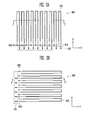
- FIGS. 3A and 3B are plan views illustrating the structure of the EMR sensor unit illustrated in FIG. 1 .
- FIG. 3A illustrates an arrangement type of the first group of coils 610.
- FIG. 3B illustrates an arrangement type of the second group of coils 630.
- FIG. 4 is a sectional view taken along the line I-I' of a bottom substrate according to the present embodiment of the present invention.
- the first group of coils 610 of the EMR sensor unit 600 is arranged in a direction (e.g., an X-axis direction).
- a plurality of first coils 612 are formed on the bottom substrate 100 at substantially uniform intervals.
- the first terminals of the first coils 612 are coupled to an external ground power supply GND through a ground line 614.
- the second terminals of the first coils 612 are coupled to the EMR IC mounted on the FPCB 300 through the above-described EMR pad unit 120.
- the first coil 612 in the first group of coils 610 that is most adjacent the contact position is selected so that a voltage (e.g., a voltage in a predetermined level) is applied to the first coil 612.
- a transmission and reception converter (not shown) and a multiplexer (not shown) coupled thereto are provided in the EMR IC.
- the signal corresponding to a sensed touch position is transmitted to a controller in the EMR IC through a first multiplexer coupled to the second terminals and the transmission and reception converter.
- the contact position of the stylus pen may be sensed.
- the second group of coils 630 of the EMR sensor unit is arranged in a direction that crosses the first group of coils 610, that is in a direction (e.g., a Y-axis direction).
- a plurality of second coils 632, each side of which being opened, is formed having uniform intervals on the insulating layer 620.
- the first terminals of the second coils 632 are coupled to an external ground power supply GND through a ground line 634, and the second terminals of the second coils 632 are coupled to the EMR IC mounted on the FPCB through the above-described EMR pad unit 120.
- the second coil 632 in the second group of coils 630, the second coil 632 being most adjacent the contact position is selected so that a voltage (e.g., a voltage in a predetermined level) is applied to the second coil.
- a transmission and reception converter and a multiplexer coupled thereto are provided in the EMR IC.
- the signal whose touch position is sensed is transmitted to a controller in the EMR IC through a second multiplexer coupled to the second terminals and the transmission and reception converter.
- the contact position of the stylus pen may be sensed.
- the transmission and reception converter selects an operation mode in which the first group of coils 610 and the second group of coils 630 are the same.
- the touch sensing operation of the passive stylus that is performed by the EMR sensor unit 600 will be briefly described as follows.
- the EMR sensor unit 600 receives a signal from the controller provided in the EMR IC to operate.
- Coils e.g., specific coils
- Coils in the first and second groups of coils 610 and 630 are selected to induce electromagnetism and to generate an electronic wave.
- a passive stylus pen (not shown), in which a resonance circuit is provided, is resonated by the electronic wave to hold a resonance frequency for a substantially uniform time, and the EMR sensor unit 600 receives the resonance frequency to sense the contact position of the stylus pen.
- the resonance circuit provided in the passive stylus pen as an RLC complex circuit
- maximum current flows at a specific frequency of an applied power supply.
- the resonance frequency might extract only the output characteristic of a specific frequency.
- the EMR sensor unit 600 has a structure in which the first group of coils 610 formed to be directly patterned on one surface of the bottom substrate 100, the insulating layer 620 formed on the front face of the bottom substrate 100 including the first group of coils 610 (e.g., on the front face of the first group of coils 610), the second group of coils 630 formed on the insulating layer 620 to be arranged in a direction that crosses the first group of coils 610, and the buffer layer 640 formed on the second group of coils 630 to planarize a surface, are sequentially laminated.
- a shield layer 650 is formed on the bottom surface of the bottom substrate 100.
- the bottom substrate 100 may be formed of, for example, a glass substrate or a material having a flexible characteristic as a transparent material.
- a transparent material for example, polyimide (PI) as a transparent material having high heat resistance and chemical resistance may be used as the flexible material.
- PI polyimide
- the plurality of pixels 112 on the bottom substrate 100, and the plurality of signal lines coupled to the pixels, are formed on the buffer layer 640.
- the structure of the EMR sensor unit 600 does not prevent the display device from displaying an image.
- the coils 612 and 632 that form the first and second groups of coils 610 and 630, respectively, are formed by patterning low resistance colored metal to maximize the performance of the EMR sensor unit 600.
- the EMR sensor unit 600 is larger than the display region 500 of the bottom substrate 100.
- the touch screen panel is directly formed on one surface of the top substrate 200 of the display device.
- FIG. 5 is an enlarged view of a main part illustrating an example of the sensing pattern of the embodiment illustrated in FIG. 1 .
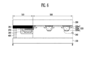
- FIG. 6 is a sectional view taken along the line II-II' of the top substrate of the embodiment illustrated in FIG. 1 .
- the sensing patterns 220 include a plurality of first sensing cells 220a formed to be coupled by row line in a first direction (e.g., the X-axis direction), first coupling lines 220a1 for coupling the first sensing cells 220a in the first direction, second sensing cells 220b formed to be coupled by column line in a second direction (e.g., the Y-axis direction), and second coupling lines 220b1 for coupling the second sensing cells 220b in the second direction.
- first direction e.g., the X-axis direction
- first coupling lines 220a1 for coupling the first sensing cells 220a in the first direction
- second sensing cells 220b formed to be coupled by column line in a second direction (e.g., the Y-axis direction)
- second coupling lines 220b1 for coupling the second sensing cells 220b in the second direction.
- the first sensing cells 220a and the second sensing cells 220b are alternately arranged so as to not overlap each other.
- the first coupling lines 220a1 and the second coupling lines 220b1 cross each other.
- An insulating layer (not shown) for securing stability is interposed between the first coupling lines 220a1 and the second coupling lines 220b1.
- the first sensing cells 220a and the second sensing cells 220b are integrated with the first coupling lines 220a1 and the second coupling lines 220b1, respectively, using a transparent electrode material such as, for example, indium tin oxide (ITO), or are formed to be separated from the first coupling lines 220a1 and the second coupling lines 220b1 to be electrically coupled.
- a transparent electrode material such as, for example, indium tin oxide (ITO)
- the second sensing cells 220b are patterned to be integrated with the second coupling lines 220b1 in the second direction, and the first sensing cells 220a are patterned among the second sensing cells 220b to have independent patterns and may be coupled by the first coupling lines 220a1 positioned on or under the first sensing cells 220a in the first direction.
- the first coupling lines 220a1 directly contact the first sensing cells 220a on or under the first sensing cells 220a to be electrically coupled, or may be directly coupled to the first sensing cells 220a through a contact hole.
- the first coupling lines 220a1 may be formed of a transparent electrode material such as, for example, ITO or an opaque low resistance material, so that the width of the first coupling lines 220a1 prevents the patterns from being noticeable.
- the sensing lines 230 are electrically coupled to the first and second sensing cells 220a and 220b in units of row and column lines to couple the first and second sensing cells 220a and 220b to an external touch IC (not shown), such as a position detecting circuit, through a first bonding pad unit 20a.
- an external touch IC not shown
- a position detecting circuit such as a position detecting circuit
- the sensing lines 230 are arranged in a non-display region 510a positioned on the outline of a display region where an image is displayed.
- the range of choice of materials of the sensing lines 230 is wide so that the sensing lines 230 may be formed of low resistance materials such as, for example, Mo, Ag, Ti, Cu, Ti, and Mo/Al/Mo other than a transparent electrode material used for forming the sensing patterns 220.
- FIG. 6 is a sectional view taken along the line II-II' of the top substrate of the embodiment illustrated in FIG. 1 .
- the sensing patterns 220 formed on the display region 500 of the top substrate 200 include the first sensing cells 220a formed to be coupled by row line in a row direction (e.g., the first direction), the first coupling lines 220a1 for coupling the first sensing cells 220a in the row direction, the second sensing cells 220b formed to be coupled by column line in a column direction, and the second coupling lines 220b1 for coupling the second sensing cells 220b in the column direction.
- An insulating layer 240 is interposed at crossing regions of the first coupling lines 220a1 and the second coupling lines 220b1.
- a black matrix 210 is formed, the sensing lines 230 electrically coupled to the sensing patterns 220 are formed with respect to the non-display region 510 that overlaps the black matrix, and the sealing material 400 is formed to attach the top substrate 200 to the bottom substrate 100.
- the black matrix 210 prevents the patterns such as the sensing lines formed in the non-display region 510 from being noticeable and forms the frame of the display region.
Landscapes
- Engineering & Computer Science (AREA)
- General Engineering & Computer Science (AREA)
- Theoretical Computer Science (AREA)
- Physics & Mathematics (AREA)
- Human Computer Interaction (AREA)
- General Physics & Mathematics (AREA)
- Electromagnetism (AREA)
- Computer Networks & Wireless Communication (AREA)
- Position Input By Displaying (AREA)
- Devices For Indicating Variable Information By Combining Individual Elements (AREA)
Abstract
Description
- Embodiments of the present invention relate to a display device capable of sensing touch.
- Touch screen panels are used as input units of smart phones and smart pads, which are currently widely used. A touch screen panel is an input device capable of enabling the selection of information or content displayed on a screen of a display device by using a user's finger to input the user's command. Therefore, the touch screen panel is provided on a front face of the display device to convert a contact position of the user's finger into an electrical signal. Therefore, the instruction contact selected by the contact position is received as an input signal.
- Since the touch screen panel may replace other input devices coupled to the image display device, such as a keyboard and a mouse, the use range thereof is increasing. Methods of realizing a touch screen panel include a resistance layer method, a photo-sensing method, and an electro-capacitive method. Among the above methods, the electro-capacitive touch screen panel is widely used, and detects change in capacitance between conductive sensing patterns and other peripheral sensing patterns or a ground electrode when the finger contacts the touch screen panel, thereby converting the contact position into the electrical signal.
- The electro-capacitive touch screen panel is commonly attached to the external surface of a display device, such as a liquid crystal display (LCD) and an organic light emitting display (OLED). However, since an additional touch screen panel is attached to the display device, the overall thickness and manufacturing cost of the display device increase and visibility of an image deteriorates due to a gap between the touch screen panel and a display panel.
- In addition, since a display device driving integrated circuit (IC) and a touch screen panel driving IC are additionally provided, products are not easily compatible with each other. Since the display device driving IC and the touch screen panel driving IC are coupled to separate flexible printed circuit boards (FPCB), respectively, manufacturing processes are complicated and product cost increases.
- In addition, recently, a pen enabling a pen input function capable of performing more delicate or more precise work, as compared to that of a finger touch, are increasingly desired. A pen applied to the conventional electro-capacitive touch screen panel generates a specific signal by internal battery power supply, and the sensing electrodes of the touch screen panel sense the signal. However, since a battery is mounted in the pen, the size of the pen increases, and the battery must be changed periodically.
- Accordingly, embodiments of the present invention provide a display device in which an electromagnetic resonance (EMR) sensor unit for sensing the contact of a stylus pen is formed on one surface of a substrate to reduce or minimize the thickness of the display device and to sense a touch more precisely.
- Embodiments of the present invention also provide a display device in which the EMR sensor unit and the display device are coupled to a single flexible printed circuit board (FPCB) to simplify manufacturing processes and to reduce product cost. Embodiments of the present invention also provide a display device whose top substrate is used as the substrate of a touch screen panel to reduce or minimize the thickness of the display device, and to improve visibility of an image.
- To achieve the foregoing and/or other aspects of embodiments of the present invention, according to one embodiment of the present invention, there is provided a display device including a plurality of pixels at a display region of a first substrate, and an electromagnetic resonance (EMR) sensor unit at one surface of the first substrate, the EMR sensor unit including a first group of coils and a second group of coils, the first group of coils and the second group of coils being laminated, wherein the EMR sensor unit is beneath the plurality of pixels.
- The EMR sensor unit may further include an insulating layer on a front face of the first group of coils, and a planarized buffer layer on the second group of coils, the first group of coils may be directly on one surface of the first substrate, and the second group of coils may be on the insulating layer and may be arranged in a direction that crosses the first group of coils.
- The plurality of pixels may be at the buffer layer.
- The EMR sensor unit may be wider than the display region of the first substrate.
- The first group of coils and the second groups of coils may include first coils and second coils arranged in a first direction and a second direction, respectively, and the first and second coils may include first terminals coupled to a ground power supply, and second terminals coupled to an EMR pad unit coupled to an EMR IC.
- The first coils and the second coils may include a patterned low resistance colored metal.
- The display device may further include a shield layer at a bottom surface of the first substrate.
- The first substrate may be transparent and may include a glass substrate or a material having a flexible characteristic.
- The first substrate may include polyimide.
- According to another embodiment of the present invention, there is provided a display device having a touch sensing function, the display device including a plurality of pixels at a display region of a first substrate, signal lines coupled to the plurality of pixels and located at a non-display region at an outline of the display region of the first substrate, an EMR sensor unit between a top surface of the first substrate and a bottom surface of the plurality of pixels, the EMR sensor unit including a first group of coils and a second group of coils, the first group of coils and the second group of coils being laminated, a driving pad unit electrically coupled to the signal lines and located at one end of the non-display region, and an EMR pad unit at a same surface as the driving pad unit to be adjacent the driving pad unit and electrically coupled to the EMR sensor unit.
- The driving pad unit and the EMR pad unit may be electrically coupled to a flexible printed circuit board (FPCB).
- The EMR sensor unit may further include an insulating layer on a front surface of the first group of coils, and a planarizing buffer layer on the second group of coils, and the first group of coils may be directly on one surface of the first substrate, and the second group of coils may be on the insulating layer and arranged in a direction that crosses the first group of coils.
- The first group of coils and the second group of coils may include first coils and second coils arranged in a first direction and a second direction, respectively, and the first coils and the second coils may include first terminals coupled to a ground power supply, and second terminals coupled to the EMR pad unit coupled to an EMR IC.
- First lines and second lines extending from the first group of coils and the second group of coils may be electrically coupled to pads of the EMR pad unit through a contact hole.
- According to another embodiment of the present invention, there is provided a display device having a touch sensing function, the display device including a plurality of pixels at a display region of a first substrate, signal lines coupled to the plurality of pixels and located at a non-display region at an outline of the display region of the first substrate, an EMR sensor unit between a top surface of the first substrate and a bottom surface of the plurality of pixels, and including a first group of coils and a second group of coils, the first group of coils and the second group of coils being laminated, a second substrate on the first substrate to seal the first substrate, the second substrate having a display region and a non-display region at the outline of the display region of the second substrate, a plurality of sensing patterns at the display region of the second substrate, a plurality of sensing lines coupled to sensing patterns and located at the non-display region of the second substrate, and a sealing material at an edge of the non-display region of the second substrate to couple the first substrate and the second substrate to each other.
- The display device may further include a first touch pad unit at the non-display region of the second substrate and overlapping the sealing material to be electrically coupled to a plurality of sensing lines.
- The display device may further include a driving pad unit at one end of the non-display region of the first substrate to be electrically coupled to the signal lines, an EMR pad unit at a same surface as, and next to, the driving pad unit, and electrically coupled to the EMR sensor unit, and a second touch pad unit at the same surface as, and next to, the driving pad unit, and electrically coupled to the first touch pad unit.
- A plurality of pads of the first touch pad unit may be electrically coupled to pads of the second touch pad unit through a plurality of conductive media in the sealing material. The driving pad unit, the EMR pad unit, and the second touch pad unit may be electrically coupled to a flexible printed circuit board (FPCB).
- The EMR sensor unit may further include an insulting layer on a front face of the first group of coils, and a planarized buffer layer on the second group of coils, and the first group of coils may be directly on one surface of the first substrate, and the second group of coils may be on the insulating layer and may be arranged in a direction that crosses the first group of coils.
- The first group of coils and the second group of coils may include first coils and second coils arranged in a first direction and a second direction, respectively, and the first coils and the second coils may include first terminals coupled to a ground power supply, and second terminals coupled to an EMR pad unit coupled to an EMR IC.
- First lines and second lines extending from the first group of coils and the second group of coils may be electrically coupled to pads of the EMR pad unit through a contact hole.
- The sensing patterns may include first sensing cells coupled by row line in a first direction, first coupling lines for coupling the first sensing cells in the first direction, second sensing cells coupled by column line in a second direction, and second coupling lines for coupling the second sensing cells in the second direction.
- The sensing patterns may be at a same layer.
- The second sensing cells may be integrated with the second coupling lines.
- The display device may further include an insulating layer at crossing regions of the first coupling lines and the second coupling lines.
- The sensing patterns are at an internal surface of the second substrate that faces the first substrate.
- In embodiments of the present invention, the EMR sensor unit for sensing contact of the stylus pen is formed on one surface of the substrate of the display device to reduce or minimize the thickness of the display device, and to sense a touch more precisely.
- In addition, the EMR sensor unit and the display device are coupled to one FPCB so that it is possible to simplify manufacturing processes and to reduce product cost.
- In addition, the top substrate of the display device may also be used as the substrate of the touch screen panel. The touch screen panel and the EMR sensor unit are mounted on the top and bottom of the display device, respectively. Therefore, it is possible to reduce or minimize the thickness of the display device, to improve visibility of an image, and to sense a touch more precisely.
- The accompanying drawings, together with the specification, illustrate exemplary embodiments of the present invention, and, together with the description, serve to explain aspects of the present invention.
-
FIG. 1 is an exploded plan view of a display device according to an embodiment of the present invention; -
FIGS. 2A and 2B are sectional views illustrating a coupling type of the pad units of the embodiment illustrated inFIG. 1 ; -
FIGS. 3A and 3B are plan views illustrating the structure of the EMR sensor unit of the embodiment illustrated inFIG. 1 ; -
FIG. 4 is a sectional view taken along the line I-I' of a bottom substrate according to the embodiment of the present invention illustrated inFIG. 3 ; -
FIG. 5 is an enlarged view of a main part illustrating an example of the sensing pattern of the embodiment illustrated inFIG. 1 ; and -
FIG. 6 is a sectional view taken along the line 11-11' of the top substrate of the embodiment illustrated inFIG. 1 . - In the following detailed description, only certain exemplary embodiments of the present invention have been shown and described, simply for the purpose of illustration. As those skilled in the art would realize, the described embodiments may be modified in various ways. Accordingly, the drawings and description are to be regarded as illustrative in nature, and not restrictive. In addition, when an element is referred to as being "on" another element, it can be directly on the other element, or can be indirectly on the other element with one or more intervening elements interposed there between. Also, when an element is referred to as being "connected to" or "coupled to" another element, it can be directly connected to another element or be indirectly connected to the other element with one or more intervening elements interposed there between. Hereinafter, like reference numerals refer to like elements. Hereinafter, embodiments of the present invention will be described in detail with reference to the accompanying drawings.
- In the present embodiment of the present invention, an electromagnetic resonance (EMR) sensor unit is formed on one surface of the bottom substrate of a display device, and an electro-capacitive touch screen panel is formed on one surface of the top substrate of the display device, so that the entire thickness of the display device may be reduced or minimized, and so that contact or touch by a passive stylus pen (e.g., a stylus pen having no battery) and/or a finger may be sensed.
- According to the present embodiment, the display device may be, for example, a liquid crystal display (LCD) or an organic light emitting display (OLED). Since the OLED may have a flexible characteristic, the OLED may be used as the display device according to the present embodiment. Therefore, in describing the present embodiment, the OLED is taken as an example.
-
FIG. 1 is an exploded plan view of a display device according to the present embodiment of the present invention.FIGS. 2A and 2B are sectional views illustrating a coupling type of the pad units of the embodiment illustrated inFIG. 1 . - The present embodiment is applied to an OLED in which a touch screen panel and an EMR sensor unit are integrated with each other. Sensing patterns and sensing lines for realizing the touch screen panel are directly formed on one surface of the
top substrate 200 of the OLED, and a first group of coils and a second group of coils that are part of the EMR sensor unit are directly formed on one surface of thebottom substrate 100 of the OLED. - In the present embodiment, the
top substrate 200 that functions as the encapsulating substrate of the OLED may be formed of, for example, a glass material or a thin film having a flexible characteristic. In addition, one surface of thetop substrate 200 may be the internal surface of the top substrate. Therefore, one surface of the top substrate illustrated inFIG. 1 corresponds to the internal surface of the top substrate. - The above is only one embodiment, and the present invention is not limited to the above. That is, sensing
patterns 220 of the touch screen panel may be formed on the external surface of thetop substrate 200, and/or may be formed on the internal and external surfaces of the top substrate. - In addition, in the present embodiment, the EMR sensor unit is mounted on the
bottom substrate 100. When a passive stylus pen including a resonance circuit contacts the display device, coils in the EMR sensor unit adjacent the contact position form a magnetic field. The EMR sensor unit senses the resonance frequency of the resonance circuit, the resonance frequency being generated by the resonance circuit resonating with the magnetic field, to determine the contact position. - The structure of the display device according to the present embodiment will be described in detail with reference to
FIG. 1 . - In the display device according to the present embodiment,
sensing patterns 220 of a touch screen panel, and sensinglines 230 for coupling thesensing patterns 220 to an external touch integrated circuit (IC) (not shown) through a firsttouch pad unit 119a, are formed on one surface of atop substrate 200 that seals abottom substrate 100 with respect to a plurality ofpixels 112 formed in adisplay region 500 of thebottom substrate 100. Also an EMR sensor unit (not shown) realized by a lamination structure of a first group of coils (not shown) and a second group of coils (not shown) is formed on one surface of thebottom substrate 100 where the plurality ofpixels 112 are formed. That is, the EMR sensor unit is directly formed on one surface of thebottom substrate 100, and the plurality ofpixels 112 are formed on a region that overlaps the EMR sensor unit. - In the present embodiment, the
sensing patterns 220 are formed on thedisplay region 500 of thetop substrate 200, thesensing lines 230 are formed on anon-display region 510 positioned on the outline of thedisplay region 500, and a sealingmaterial 400 for attaching thetop substrate 200 to thebottom substrate 100 is coated at the edge of thenon-display region 510. - In addition, a plurality of
signal lines pixels 112 formed on thedisplay region 500 of thebottom substrate 100, and thesignal lines non-display region 510. - In
FIG. 1 ,scan lines 114 anddata lines 116 are arranged as the signal lines. However, emission control lines for controlling emission of organic light emitting diodes (OLED) provided in pixels may also be provided. - In the present embodiment, the pixels include OLEDs that are self-emissive elements, a plurality of transistors, and at least one capacitor.
- As illustrated in
FIG. 1 , thesignal lines driving pad unit 118 provided at one end of thenon-display region 510 of thebottom substrate 100 to receive signals from an external driving IC (not shown) mounted on a flexible printed circuit board (FPCB) 300. - In addition, a second
touch pad unit 119b and anEMR pad unit 120 are adjacently located on side surfaces of thedriving pad unit 118, respectively. The EMR sensor unit is electrically coupled to theEMR pad unit 120. The firsttouch pad unit 119a formed on thetop substrate 200 is electrically coupled to the secondtouch pad unit 119b. - Coupling of the first
touch pad unit 119a formed on thetop substrate 200 to the secondtouch pad unit 119b formed on thebottom substrate 100 may be realized by the present embodiment illustrated inFIG. 2A . That is, the firsttouch pad unit 119a on the top substrate overlaps the sealingmaterial 400, and a plurality of pads that form the firsttouch pad unit 119a are electrically coupled to the pads of the secondtouch pad unit 119b, which are located at one end of the non-display region of the bottom substrate, through a plurality of conductive media (for example, a conductive ball/conductive member 410) provided in the sealingmaterial 400. - Next, as illustrated in
FIG. 2B , in anEMR sensor unit 600 directly formed on one surface of thebottom substrate 100, a plurality offirst lines 612 withdrawn from a first group ofcoils 610, and a plurality ofsecond lines 632 withdrawn from a second group ofcoils 630, are electrically coupled to the pads of theEMR pad unit 120 located at one end of the non-display region of thebottom substrate 100 through acontact hole 602. - The
EMR sensor unit 600 has a structure in which a first group ofcoils 610 are directly patterned on one surface of thebottom substrate 100, an insulatinglayer 620 formed on the front face of thebottom substrate 100 including the first group of coils 610 (e.g., on the front face of the first group of coils 610), a second group ofcoils 630 formed on the insulatinglayer 620 to be arranged in a direction that crosses the first group ofcoils 610, and a buffer layer 640 (e.g., a planarized buffer layer 640) formed on the second group ofcoils 630 to planarize a surface, are sequentially laminated. The structure of the EMR sensor unit will be described in detail with reference toFIGS. 3 and4 . - In the above-described structure, the pad units provided at one end of the
non-display region 510 of thebottom substrate 100, that is, thedriving pad unit 118, the secondtouch pad unit 119b, and theEMR pad unit 120 are electrically coupled to thesame FPCB 300. - In addition, a driving IC (not shown) for driving a plurality of pixels (not shown) in the pixel region of the
bottom substrate 100, a touch IC (not shown) for controlling the operations of thesensing patterns 220 on thetop substrate 200, and an EMR IC (not shown) for controlling the operation of theEMR sensor unit 600 on one surface of the bottom substrate may be mounted on theFPCB 300. In the present embodiment, the driving IC, the touch IC, and the EMR IC may be realized by separate ICs, or may be realized by an integrated IC for realizing all of the functions. In the present embodiment, theFPCB 300 is integrated into one to simplify bonding and testing processes of theFPCB 300 and to reduce or minimize manufacturing processes and product cost. - In the present embodiment, as described above, the EMR sensor unit is directly on one surface of the bottom substrate of the display device.
-
FIGS. 3A and 3B are plan views illustrating the structure of the EMR sensor unit illustrated inFIG. 1 .FIG. 3A illustrates an arrangement type of the first group ofcoils 610.FIG. 3B illustrates an arrangement type of the second group ofcoils 630. -
FIG. 4 is a sectional view taken along the line I-I' of a bottom substrate according to the present embodiment of the present invention. - First, referring to
FIG. 3A , the first group ofcoils 610 of theEMR sensor unit 600 is arranged in a direction (e.g., an X-axis direction). In the first group ofcoils 610, a plurality offirst coils 612, one side of each of which being opened, are formed on thebottom substrate 100 at substantially uniform intervals. - The first terminals of the
first coils 612 are coupled to an external ground power supply GND through aground line 614. The second terminals of thefirst coils 612 are coupled to the EMR IC mounted on theFPCB 300 through the above-describedEMR pad unit 120. When a stylus pen makes contact, thefirst coil 612 in the first group ofcoils 610 that is most adjacent the contact position is selected so that a voltage (e.g., a voltage in a predetermined level) is applied to thefirst coil 612. - In the present embodiment, a transmission and reception converter (not shown) and a multiplexer (not shown) coupled thereto are provided in the EMR IC. During a transmission operation, the signal corresponding to a sensed touch position is transmitted to a controller in the EMR IC through a first multiplexer coupled to the second terminals and the transmission and reception converter. During a reception operation, the contact position of the stylus pen may be sensed.
- Similarly, referring to
FIG. 3B , the second group ofcoils 630 of the EMR sensor unit is arranged in a direction that crosses the first group ofcoils 610, that is in a direction (e.g., a Y-axis direction). A plurality ofsecond coils 632, each side of which being opened, is formed having uniform intervals on the insulatinglayer 620. - The first terminals of the
second coils 632 are coupled to an external ground power supply GND through aground line 634, and the second terminals of thesecond coils 632 are coupled to the EMR IC mounted on the FPCB through the above-describedEMR pad unit 120. When a stylus pen makes a contact, thesecond coil 632 in the second group ofcoils 630, thesecond coil 632 being most adjacent the contact position, is selected so that a voltage (e.g., a voltage in a predetermined level) is applied to the second coil. - In the present embodiment, a transmission and reception converter and a multiplexer coupled thereto are provided in the EMR IC. During a transmission operation, the signal whose touch position is sensed is transmitted to a controller in the EMR IC through a second multiplexer coupled to the second terminals and the transmission and reception converter. During a reception operation, the contact position of the stylus pen may be sensed.
- Here, the transmission and reception converter selects an operation mode in which the first group of
coils 610 and the second group ofcoils 630 are the same. - The touch sensing operation of the passive stylus that is performed by the
EMR sensor unit 600 will be briefly described as follows. TheEMR sensor unit 600 receives a signal from the controller provided in the EMR IC to operate. Coils (e.g., specific coils) in the first and second groups ofcoils - A passive stylus pen (not shown), in which a resonance circuit is provided, is resonated by the electronic wave to hold a resonance frequency for a substantially uniform time, and the
EMR sensor unit 600 receives the resonance frequency to sense the contact position of the stylus pen. - Here, in the resonance circuit provided in the passive stylus pen as an RLC complex circuit, maximum current flows at a specific frequency of an applied power supply. The resonance frequency might extract only the output characteristic of a specific frequency.
- Referring to
FIG. 4 , theEMR sensor unit 600 according to the present embodiment has a structure in which the first group ofcoils 610 formed to be directly patterned on one surface of thebottom substrate 100, the insulatinglayer 620 formed on the front face of thebottom substrate 100 including the first group of coils 610 (e.g., on the front face of the first group of coils 610), the second group ofcoils 630 formed on the insulatinglayer 620 to be arranged in a direction that crosses the first group ofcoils 610, and thebuffer layer 640 formed on the second group ofcoils 630 to planarize a surface, are sequentially laminated. Ashield layer 650 is formed on the bottom surface of thebottom substrate 100. - The
bottom substrate 100 may be formed of, for example, a glass substrate or a material having a flexible characteristic as a transparent material. For example, polyimide (PI) as a transparent material having high heat resistance and chemical resistance may be used as the flexible material. - The plurality of
pixels 112 on thebottom substrate 100, and the plurality of signal lines coupled to the pixels, are formed on thebuffer layer 640. - Since the
EMR sensor unit 600 is provided on one surface of thebottom substrate 100 of the organic light emitting display that operates in a top emission method, that is, under the plurality ofpixels 112, the structure of theEMR sensor unit 600 does not prevent the display device from displaying an image. - Therefore, in the present embodiment, the
coils coils EMR sensor unit 600. - In addition, it is relatively easy for a user to draw a desired figure as the area of the
EMR sensor unit 600 is relatively larger. Therefore, theEMR sensor unit 600 according to the present embodiment is larger than thedisplay region 500 of thebottom substrate 100. - In addition, in the present embodiment, as described above, the touch screen panel is directly formed on one surface of the
top substrate 200 of the display device. -
FIG. 5 is an enlarged view of a main part illustrating an example of the sensing pattern of the embodiment illustrated inFIG. 1 .FIG. 6 is a sectional view taken along the line II-II' of the top substrate of the embodiment illustrated inFIG. 1 . - The structure of the touch screen panel according to the present embodiment will be described in detail with reference to
FIGS. 1 ,5 , and6 . - As illustrated in
FIG. 5 , thesensing patterns 220 include a plurality offirst sensing cells 220a formed to be coupled by row line in a first direction (e.g., the X-axis direction), first coupling lines 220a1 for coupling thefirst sensing cells 220a in the first direction,second sensing cells 220b formed to be coupled by column line in a second direction (e.g., the Y-axis direction), and second coupling lines 220b1 for coupling thesecond sensing cells 220b in the second direction. - The
first sensing cells 220a and thesecond sensing cells 220b are alternately arranged so as to not overlap each other. The first coupling lines 220a1 and the second coupling lines 220b1 cross each other. An insulating layer (not shown) for securing stability is interposed between the first coupling lines 220a1 and the second coupling lines 220b1. - On the other hand, the
first sensing cells 220a and thesecond sensing cells 220b are integrated with the first coupling lines 220a1 and the second coupling lines 220b1, respectively, using a transparent electrode material such as, for example, indium tin oxide (ITO), or are formed to be separated from the first coupling lines 220a1 and the second coupling lines 220b1 to be electrically coupled. - For example, the
second sensing cells 220b are patterned to be integrated with the second coupling lines 220b1 in the second direction, and thefirst sensing cells 220a are patterned among thesecond sensing cells 220b to have independent patterns and may be coupled by the first coupling lines 220a1 positioned on or under thefirst sensing cells 220a in the first direction. - In the present embodiment, the first coupling lines 220a1 directly contact the
first sensing cells 220a on or under thefirst sensing cells 220a to be electrically coupled, or may be directly coupled to thefirst sensing cells 220a through a contact hole. - The first coupling lines 220a1 may be formed of a transparent electrode material such as, for example, ITO or an opaque low resistance material, so that the width of the first coupling lines 220a1 prevents the patterns from being noticeable.
- The sensing lines 230 are electrically coupled to the first and
second sensing cells second sensing cells - The sensing lines 230 are arranged in a non-display region 510a positioned on the outline of a display region where an image is displayed. The range of choice of materials of the
sensing lines 230 is wide so that thesensing lines 230 may be formed of low resistance materials such as, for example, Mo, Ag, Ti, Cu, Ti, and Mo/Al/Mo other than a transparent electrode material used for forming thesensing patterns 220. When a finger contacts the above-described electro-capacitive touch screen panel, a change in capacitance in accordance with the contact position is transmitted from thesensing patterns 220 to a touch IC (not shown) via thesensing lines 230 and the first and secondtouch pad units - In addition,
FIG. 6 is a sectional view taken along the line II-II' of the top substrate of the embodiment illustrated inFIG. 1 . Referring toFIG. 6 , as described above, thesensing patterns 220 formed on thedisplay region 500 of thetop substrate 200 include thefirst sensing cells 220a formed to be coupled by row line in a row direction (e.g., the first direction), the first coupling lines 220a1 for coupling thefirst sensing cells 220a in the row direction, thesecond sensing cells 220b formed to be coupled by column line in a column direction, and the second coupling lines 220b1 for coupling thesecond sensing cells 220b in the column direction. An insulatinglayer 240 is interposed at crossing regions of the first coupling lines 220a1 and the second coupling lines 220b1. In addition, in thenon-display region 510 of thetop substrate 200 positioned on the outline of thedisplay region 500, ablack matrix 210 is formed, thesensing lines 230 electrically coupled to thesensing patterns 220 are formed with respect to thenon-display region 510 that overlaps the black matrix, and the sealingmaterial 400 is formed to attach thetop substrate 200 to thebottom substrate 100. - In the present embodiment, the
black matrix 210 prevents the patterns such as the sensing lines formed in thenon-display region 510 from being noticeable and forms the frame of the display region.
Claims (19)
- A display device comprising:a plurality of pixels (112) at a display region (500) of a first substrate (100); andan electromagnetic resonance (EMR) sensor unit (600) at one surface of the first substrate (100), the EMR sensor unit (600) comprising a first group of coils (610) and a second group of coils (630), the first group of coils (610) and the second group of coils (630) being laminated,wherein the EMR sensor (600) unit is beneath the plurality of pixels (112).
- The display device as claimed in claim 1,
wherein the EMR sensor unit (600) further comprises:an insulating layer (620) on a front face of the first group of coils (610); anda planarized buffer layer (640) on the second group of coils (630),wherein the first group of coils (610) is directly on one surface of the first substrate (100), and
wherein the second group of coils (630) is on the insulating layer (620) and is arranged in a direction that crosses the first group of coils (610). - The display device as claimed in claim 2, wherein the plurality of pixels (112) are at the buffer layer (640).
- The display device as claimed in any of claims 1 to 3, wherein the EMR sensor unit (600) is wider than the display region (500) of the first substrate (100).
- The display device as claimed in any of claims 1 to 4,
wherein the first group of coils (610) and the second groups of coils (630) comprise first coils and second coils arranged in a first direction and a second direction, respectively, and
wherein the first and second coils comprises:first terminals coupled to a ground power supply; andsecond terminals coupled to an EMR pad unit (120) coupled to an EMR IC. - The display device as claimed in any of claims 1 to 5, wherein the first coils and the second coils comprise a patterned low resistance colored metal.
- The display device as claimed in any of claims 1 to 6, further comprising a shield layer at a bottom surface of the first substrate (100).
- The display device as claimed in any of claims 1 to 7, wherein the first substrate (100) is transparent and comprises a glass substrate or a material having a flexible characteristic.
- The display device as claimed in any of claims 1 to 8, wherein the first substrate (100) comprises polyimide.
- The display device as claimed in any of claims 1 to 9, the display device having a touch sensing function, the display device further comprising:signal lines (114, 116) coupled to the plurality of pixels (112) and located at a non-display region (510) at an outline of the display region (500) of the first substrate (100);the EMR sensor unit (600) between a top surface of the first substrate (100) and a bottom surface of the plurality of pixels (112);a driving pad unit (118) electrically coupled to the signal lines (114, 116) and located at one end of the non-display region (510); andan EMR pad unit (120) at a same surface as the driving pad unit (118) to be adjacent the driving pad unit (118) and electrically coupled to the EMR sensor unit (600).
- The display device as claimed in claim 10 , the display device comprising:a second substrate (200) on the first substrate (100) to seal the first substrate (100), the second substrate (200) having a display region and a non-display region (51 Oa) at the outline of the display region of the second substrate (200);a plurality of sensing patterns (220) at the display region of the second substrate (200);a plurality of sensing lines (632) coupled to sensing patterns (220) and located at the non-display region of the second substrate (200); anda sealing material (400) at an edge of the non-display region of the second substrate (200) to couple the first substrate (100) and the second substrate (200) to each other.
- The display device as claimed in claim 11, further comprising a first touch pad unit at the non-display region (510a) of the second substrate (200) and overlapping the sealing material (400) to be electrically coupled to a plurality of sensing lines (230).
- The display device as claimed in claim 12, further comprising:the driving pad unit (118) at one end of the non-display region (510) of the first substrate (100) to be electrically coupled to the signal lines (114, 116);the EMR pad unit (120) at a same surface as, and next to, the driving pad unit (118), and electrically coupled to the EMR sensor unit (600); anda second touch pad unit at the same surface as, and next to, the driving pad unit (118), and electrically coupled to the first touch pad unit.
- The display device as claimed in claim 13, wherein a plurality of pads of the first touch pad unit are electrically coupled to pads of the second touch pad unit through a plurality of conductive media in the sealing material (400).
- The display device as claimed in any of claims 11 to 14, wherein the sensing patterns comprise:first sensing cells (220a) coupled by row line in a first direction;first coupling lines (220a1) for coupling the first sensing cells (220a) in the first direction;second sensing cells (220b) coupled by column line in a second direction; andsecond coupling lines (220b1) for coupling the second sensing cells (220b) in the second direction.
- The display device as claimed in any of claims 11 to 15, wherein the sensing patterns (220) are at a same layer.
- The display device as claimed in claims 15 or 16, wherein the second sensing cells (220b) are integrated with the second coupling lines (220b1).
- The display device as claimed in any of claims 15 to 17, further comprising an insulating layer at crossing regions of the first coupling lines (220a1) and the second coupling lines (220b1).
- The display device as claimed in any of claims 11 to 18, wherein the sensing patterns (220) are at an internal surface of the second substrate (200) that faces the first substrate (100).
Applications Claiming Priority (1)
| Application Number | Priority Date | Filing Date | Title |
|---|---|---|---|
| KR1020120077785A KR101391243B1 (en) | 2012-07-17 | 2012-07-17 | display device having touch sensing function |
Publications (2)
| Publication Number | Publication Date |
|---|---|
| EP2687963A2 true EP2687963A2 (en) | 2014-01-22 |
| EP2687963A3 EP2687963A3 (en) | 2016-08-10 |
Family
ID=47740794
Family Applications (1)
| Application Number | Title | Priority Date | Filing Date |
|---|---|---|---|
| EP13152963.8A Withdrawn EP2687963A3 (en) | 2012-07-17 | 2013-01-29 | Display device having touch sensing function |
Country Status (6)
| Country | Link |
|---|---|
| US (1) | US9158398B2 (en) |
| EP (1) | EP2687963A3 (en) |
| JP (1) | JP5647202B2 (en) |
| KR (1) | KR101391243B1 (en) |
| CN (1) | CN103543898B (en) |
| TW (1) | TWI509490B (en) |
Cited By (4)
| Publication number | Priority date | Publication date | Assignee | Title |
|---|---|---|---|---|
| WO2016157012A1 (en) * | 2015-03-27 | 2016-10-06 | Semiconductor Energy Laboratory Co., Ltd. | Touch panel |
| WO2016204419A1 (en) * | 2015-06-18 | 2016-12-22 | 주식회사 아모그린텍 | Touch screen panel touch sensor comprising power coil pattern for electronic pen, manufacturing method therefor, and touch screen panel comprising same |
| EP3126938A4 (en) * | 2014-03-31 | 2017-11-15 | LG Innotek Co., Ltd. | Touch panel for improving cross structure of sensing pattern |
| EP3413180A1 (en) * | 2017-06-07 | 2018-12-12 | LG Display Co., Ltd. | Organic light-emitting display device having touchscreen and method of manufacturing the same |
Families Citing this family (33)
| Publication number | Priority date | Publication date | Assignee | Title |
|---|---|---|---|---|
| US9471174B2 (en) * | 2013-07-01 | 2016-10-18 | Electronics And Telecommunications Research Institute | Control apparatus and method of addressing two-dimensional signal |
| KR102193915B1 (en) * | 2014-02-10 | 2020-12-23 | 삼성디스플레이 주식회사 | Touch sensor substrate and display apparatus having the touch sensor substrate |
| KR101581412B1 (en) * | 2014-04-01 | 2015-12-30 | (주)엔피홀딩스 | Digitizer |
| CN104978056B (en) * | 2014-04-02 | 2018-08-14 | 宝宸(厦门)光学科技有限公司 | touch panel |
| KR102239861B1 (en) * | 2014-11-26 | 2021-04-13 | 삼성디스플레이 주식회사 | Display device including touch sensor and driving method thereof |
| KR102274576B1 (en) * | 2014-12-31 | 2021-07-06 | 엘지디스플레이 주식회사 | Touch screen-integrated display device |
| WO2017045165A1 (en) * | 2015-09-16 | 2017-03-23 | 深圳迈瑞生物医疗电子股份有限公司 | Monitor, display device thereof, monitoring system |
| KR102468767B1 (en) * | 2015-12-29 | 2022-11-18 | 엘지디스플레이 주식회사 | Touch-Integrated Display Panel for Display Device |
| CN205594265U (en) | 2016-05-11 | 2016-09-21 | 合肥鑫晟光电科技有限公司 | Backlight module and display device |
| KR102610710B1 (en) * | 2016-06-10 | 2023-12-08 | 삼성디스플레이 주식회사 | Display device and fabricating method thereof |
| KR102007435B1 (en) * | 2016-08-02 | 2019-08-06 | 삼성디스플레이 주식회사 | Organic light emitting display module and organic light emitting display device having the same |
| KR20180055941A (en) * | 2016-11-16 | 2018-05-28 | 삼성디스플레이 주식회사 | Flexible display having integrated sensor and method of manufacturing the same |
| CN108091676B (en) * | 2017-12-14 | 2022-02-22 | 合肥鑫晟光电科技有限公司 | Touch display substrate, manufacturing method thereof and touch display device |
| KR102456493B1 (en) * | 2017-12-21 | 2022-10-20 | 삼성디스플레이 주식회사 | Display device |
| KR102054817B1 (en) * | 2018-02-06 | 2019-12-12 | (주)파트론 | Touch sensor module and touch panel having the same |
| KR101996984B1 (en) * | 2018-03-05 | 2019-07-08 | 주식회사 지2터치 | Display apparatus with touch function and signal line mounting method of display apparatus |
| KR102264326B1 (en) * | 2019-05-31 | 2021-06-14 | (주)파트론 | Touch sensor module |
| KR102195091B1 (en) * | 2019-07-02 | 2020-12-24 | (주)파트론 | Touch sensor module and touch panel having the same |
| KR102890658B1 (en) * | 2020-03-12 | 2025-11-25 | 삼성디스플레이 주식회사 | Display device |
| KR102376400B1 (en) * | 2020-05-06 | 2022-03-18 | 고려대학교 산학협력단 | Electro magnetic resonance sensor panel and display device including same |
| KR20220049066A (en) * | 2020-10-13 | 2022-04-21 | 삼성디스플레이 주식회사 | Display device |
| TWI818421B (en) * | 2021-01-29 | 2023-10-11 | 南韓商希迪普公司 | Touch device, driving method the same and touch system |
| DE112021004797T5 (en) * | 2021-02-02 | 2023-07-27 | Wacom Co., Ltd. | SENSOR BOARD AND INDICATOR |
| EP4239458A4 (en) | 2021-02-09 | 2024-02-21 | Samsung Electronics Co., Ltd. | DIGITIZER PANEL AND ELECTRONIC DEVICE COMPRISING A DIGITIZER PANEL |
| WO2022173137A1 (en) * | 2021-02-09 | 2022-08-18 | 삼성전자 주식회사 | Digitizer panel and electronic device comprising digitizer panel |
| KR20220148986A (en) | 2021-04-29 | 2022-11-08 | 삼성디스플레이 주식회사 | Electronic device and interface device including the same |
| CN114924665A (en) * | 2022-05-12 | 2022-08-19 | 武汉华星光电半导体显示技术有限公司 | Touch display module and touch display device |
| JP7599741B2 (en) * | 2022-08-04 | 2024-12-16 | 株式会社 ハイディープ | Touch input system and controller including pen |
| KR20240105569A (en) * | 2022-12-28 | 2024-07-08 | 삼성디스플레이 주식회사 | Electronic apparatus and method for manufacturing of the same |
| JPWO2024237317A1 (en) * | 2023-05-16 | 2024-11-21 | ||
| CN119024599A (en) * | 2023-05-26 | 2024-11-26 | 北京京东方光电科技有限公司 | Array substrate, display panel and display device |
| KR20250018270A (en) | 2023-07-27 | 2025-02-05 | 삼성디스플레이 주식회사 | Electronic device and interface device including the same |
| KR20250064166A (en) | 2023-11-01 | 2025-05-09 | 삼성디스플레이 주식회사 | Electronic device |
Family Cites Families (33)
| Publication number | Priority date | Publication date | Assignee | Title |
|---|---|---|---|---|
| JP2002182197A (en) * | 2000-12-13 | 2002-06-26 | Kyocera Corp | Reflective liquid crystal display |
| JP4597676B2 (en) | 2002-08-29 | 2010-12-15 | エヌ−トリグ リミテッド | Transparent digitizer |
| KR100459230B1 (en) * | 2002-11-14 | 2004-12-03 | 엘지.필립스 엘시디 주식회사 | touch panel for display device |
| DE602004027705D1 (en) | 2003-02-10 | 2010-07-29 | N trig ltd | TOUCH DETECTION FOR A DIGITIZER |
| JP2004272365A (en) * | 2003-03-05 | 2004-09-30 | Seiko Epson Corp | Electro-optical panel, electro-optical device, method of manufacturing electro-optical panel, method of manufacturing electro-optical device, electromagnetic induction sensor, and electronic device |
| KR100499576B1 (en) | 2003-03-28 | 2005-07-05 | 엘지.필립스 엘시디 주식회사 | In-Plane Switching mode Liquid Crystal Display Device Having Touch Panel of Electro Magnetic Type |
| KR100510729B1 (en) | 2003-03-28 | 2005-08-30 | 엘지.필립스 엘시디 주식회사 | Liquid Crystal Display Device Having Electro Magnetic Type Touch Panel |
| US7755616B2 (en) | 2003-03-28 | 2010-07-13 | Lg Display Co., Ltd. | Liquid crystal display device having electromagnetic type touch panel |
| TWI288826B (en) | 2003-09-05 | 2007-10-21 | N trig ltd | Touch detection for a digitizer |
| WO2005055030A2 (en) | 2003-12-08 | 2005-06-16 | Canon Kabushiki Kaisha | Display apparatus |
| JP2005173709A (en) * | 2003-12-08 | 2005-06-30 | Canon Inc | Display device |
| US7924269B2 (en) * | 2005-01-04 | 2011-04-12 | Tpo Displays Corp. | Display devices and methods forming the same |
| JP2006208563A (en) | 2005-01-26 | 2006-08-10 | Toshiba Matsushita Display Technology Co Ltd | Liquid crystal display device |
| EP1746485A2 (en) * | 2005-07-21 | 2007-01-24 | TPO Displays Corp. | Process of integrating a digitizer input device in a display |
| JP4701069B2 (en) * | 2005-10-21 | 2011-06-15 | キヤノン株式会社 | Integrated display position detector |
| JP5268262B2 (en) | 2006-02-24 | 2013-08-21 | キヤノン株式会社 | Electroluminescence display device |
| KR101330214B1 (en) | 2006-07-18 | 2013-11-18 | 삼성디스플레이 주식회사 | Touch screen display apparatus and method of driving the same |
| WO2008143212A1 (en) * | 2007-05-18 | 2008-11-27 | Kabushiki Kaisha Sega Doing Business As Sega Corporation | Digitizer function-equipped liquid crystal display device, information processing electronic device, and game device |
| JP2009116090A (en) | 2007-11-07 | 2009-05-28 | Hitachi Displays Ltd | Liquid crystal display device |
| TW200930280A (en) | 2007-12-21 | 2009-07-01 | Mildex Optical Inc | Capacitive touch panel capable of resisting electromagnetic interference |
| US8482545B2 (en) | 2008-10-02 | 2013-07-09 | Wacom Co., Ltd. | Combination touch and transducer input system and method |
| TWI463452B (en) | 2009-04-21 | 2014-12-01 | Ind Tech Res Inst | Touch display apparatus and fabricating method thereof |
| TWI497157B (en) | 2009-06-19 | 2015-08-21 | Tpk Touch Solutions Inc | Touch ips liquid crystal display |
| CN101930133A (en) * | 2009-06-19 | 2010-12-29 | 台均科技(深圳)有限公司 | Liquid crystal panel and liquid crystal display |
| KR101073309B1 (en) | 2009-11-24 | 2011-10-12 | 삼성모바일디스플레이주식회사 | touch screen system and driving method thereof |
| JP5427070B2 (en) * | 2010-03-05 | 2014-02-26 | 株式会社ワコム | Position detection device |
| KR101178914B1 (en) * | 2010-10-29 | 2012-09-03 | 삼성디스플레이 주식회사 | flat panel display integrated touch screen panel |
| TWI437474B (en) * | 2010-12-16 | 2014-05-11 | Hongda Liu | Dual-modes touch sensor and touch display and driving method thereof |
| JP2012133704A (en) * | 2010-12-24 | 2012-07-12 | Wacom Co Ltd | Input device |
| KR101750564B1 (en) * | 2011-01-05 | 2017-06-23 | 삼성전자주식회사 | Digitizer integrated display module |
| JP2012221275A (en) * | 2011-04-11 | 2012-11-12 | Hosiden Corp | Touch panel and portable terminal equipment having the same |
| JP5459795B2 (en) * | 2011-06-06 | 2014-04-02 | 株式会社ワコム | Electronics |
| TWM425329U (en) | 2011-07-04 | 2012-03-21 | Edamak Corp | Magnetic and capacitive touch panel and the module using the same |
-
2012
- 2012-07-17 KR KR1020120077785A patent/KR101391243B1/en not_active Expired - Fee Related
- 2012-10-10 JP JP2012224958A patent/JP5647202B2/en active Active
- 2012-12-12 US US13/712,922 patent/US9158398B2/en active Active
-
2013
- 2013-01-16 TW TW102101579A patent/TWI509490B/en active
- 2013-01-29 EP EP13152963.8A patent/EP2687963A3/en not_active Withdrawn
- 2013-05-15 CN CN201310179812.2A patent/CN103543898B/en active Active
Non-Patent Citations (1)
| Title |
|---|
| None |
Cited By (18)
| Publication number | Priority date | Publication date | Assignee | Title |
|---|---|---|---|---|
| EP3126938A4 (en) * | 2014-03-31 | 2017-11-15 | LG Innotek Co., Ltd. | Touch panel for improving cross structure of sensing pattern |
| US10055077B2 (en) | 2014-03-31 | 2018-08-21 | Lg Innotek Co., Ltd. | Touch panel for improving cross structure of sensing pattern |
| US11048111B2 (en) | 2015-03-27 | 2021-06-29 | Semiconductor Energy Laboratory Co., Ltd. | Display device equipped touch panel |
| US10067621B2 (en) | 2015-03-27 | 2018-09-04 | Semiconductor Energy Laboratory Co., Ltd. | Touch panel |
| US12339536B2 (en) | 2015-03-27 | 2025-06-24 | Semiconductor Energy Laboratory Co., Ltd. | Display device |
| US11835810B2 (en) | 2015-03-27 | 2023-12-05 | Semiconductor Energy Laboratory Co., Ltd. | Display device |
| US11803074B2 (en) | 2015-03-27 | 2023-10-31 | Semiconductor Energy Laboratory Co., Ltd. | Display device |
| WO2016157012A1 (en) * | 2015-03-27 | 2016-10-06 | Semiconductor Energy Laboratory Co., Ltd. | Touch panel |
| WO2016204419A1 (en) * | 2015-06-18 | 2016-12-22 | 주식회사 아모그린텍 | Touch screen panel touch sensor comprising power coil pattern for electronic pen, manufacturing method therefor, and touch screen panel comprising same |
| US10566395B2 (en) | 2017-06-07 | 2020-02-18 | Lg Display Co., Ltd. | Organic light-emitting display device having touchscreen and method of manufacturing the same |
| US10818738B2 (en) | 2017-06-07 | 2020-10-27 | Lg Display Co., Ltd. | Organic light-emitting display device having touchscreen and method of manufacturing the same |
| US11569310B2 (en) | 2017-06-07 | 2023-01-31 | Lg Display Co., Ltd. | Organic light-emitting display device having touchscreen and method of manufacturing the same |
| CN109003997B (en) * | 2017-06-07 | 2023-07-25 | 乐金显示有限公司 | Organic light emitting display device having touch screen and method of manufacturing the same |
| EP4224292A1 (en) * | 2017-06-07 | 2023-08-09 | LG Display Co., Ltd. | Organic light-emitting display device having touchscreen and method of manufacturing the same |
| CN109003997A (en) * | 2017-06-07 | 2018-12-14 | 乐金显示有限公司 | Organic light-emitting display device with touch screen and the method for manufacturing the device |
| US20180358413A1 (en) * | 2017-06-07 | 2018-12-13 | Lg Display Co., Ltd. | Organic light-emitting display device having touchscreen and method of manufacturing the same |
| EP3413180A1 (en) * | 2017-06-07 | 2018-12-12 | LG Display Co., Ltd. | Organic light-emitting display device having touchscreen and method of manufacturing the same |
| EP4604698A3 (en) * | 2017-06-07 | 2025-11-19 | LG Display Co., Ltd. | Organic light-emitting display device having touchscreen and method of manufacturing the same |
Also Published As
| Publication number | Publication date |
|---|---|
| KR101391243B1 (en) | 2014-05-02 |
| TWI509490B (en) | 2015-11-21 |
| US9158398B2 (en) | 2015-10-13 |
| CN103543898B (en) | 2017-06-27 |
| EP2687963A3 (en) | 2016-08-10 |
| JP2014021964A (en) | 2014-02-03 |
| TW201405403A (en) | 2014-02-01 |
| CN103543898A (en) | 2014-01-29 |
| KR20140010799A (en) | 2014-01-27 |
| JP5647202B2 (en) | 2014-12-24 |
| US20140022187A1 (en) | 2014-01-23 |
Similar Documents
| Publication | Publication Date | Title |
|---|---|---|
| US9158398B2 (en) | Display device having touch screen sensing function | |
| JP7023904B2 (en) | Display device including touch sensor | |
| KR101309862B1 (en) | Liquid Crystal Display Device Including Touch Panel | |
| US9639218B2 (en) | Liquid crystal panel, display device and scanning method thereof | |
| CN110515496B (en) | Touch display panel, working method thereof and touch display device | |
| US11188165B2 (en) | Touch screen panel having mesh pattern electrodes with improved performance and display device including the same | |
| JP5213985B2 (en) | Display device with in-cell touch sensor device | |
| EP2911043B1 (en) | Touch window and touch device | |
| CN110007794B (en) | Display device with integrated touch screen | |
| EP2527962B1 (en) | Integrated digitizer display | |
| US20120127095A1 (en) | Flat panel display with an integrated touch screen panel | |
| CN109791452A (en) | Touch panel display with antenna | |
| KR20160088533A (en) | Touch sensor | |
| CN115454273A (en) | Touch-sensitive display device and display panel | |
| KR101703503B1 (en) | Touch sensing panel and touch sensing device for transmitting touch signal by using printed circuit board | |
| CN102221754B (en) | Display with embedded touch-control device | |
| CN106816448A (en) | Touch control display apparatus and its driving method | |
| KR20190095006A (en) | Touch input apparatus | |
| KR20200077987A (en) | Touch screen panel and touch screen integrated display Device | |
| CN113918046A (en) | Display panel, display device, manufacturing method and control method | |
| KR20250177493A (en) | Display apparatus with integrated touch screen | |
| CN113655914B (en) | Array substrate, touch display panel and touch display device | |
| CN114461087B (en) | Electronic device with touch control function | |
| KR20250131283A (en) | Display device and method for driving the same |
Legal Events
| Date | Code | Title | Description |
|---|---|---|---|
| PUAI | Public reference made under article 153(3) epc to a published international application that has entered the european phase |
Free format text: ORIGINAL CODE: 0009012 |
|
| 17P | Request for examination filed |
Effective date: 20130129 |
|
| AK | Designated contracting states |
Kind code of ref document: A2 Designated state(s): AL AT BE BG CH CY CZ DE DK EE ES FI FR GB GR HR HU IE IS IT LI LT LU LV MC MK MT NL NO PL PT RO RS SE SI SK SM TR |
|
| AX | Request for extension of the european patent |
Extension state: BA ME |
|
| RAP1 | Party data changed (applicant data changed or rights of an application transferred) |
Owner name: SAMSUNG DISPLAY CO., LTD. |
|
| PUAL | Search report despatched |
Free format text: ORIGINAL CODE: 0009013 |
|
| AK | Designated contracting states |
Kind code of ref document: A3 Designated state(s): AL AT BE BG CH CY CZ DE DK EE ES FI FR GB GR HR HU IE IS IT LI LT LU LV MC MK MT NL NO PL PT RO RS SE SI SK SM TR |
|
| AX | Request for extension of the european patent |
Extension state: BA ME |
|
| RIC1 | Information provided on ipc code assigned before grant |
Ipc: G06F 3/044 20060101ALI20160705BHEP Ipc: G06F 3/046 20060101AFI20160705BHEP |
|
| STAA | Information on the status of an ep patent application or granted ep patent |
Free format text: STATUS: THE APPLICATION HAS BEEN WITHDRAWN |
|
| 18W | Application withdrawn |
Effective date: 20170707 |