EP2685633A2 - Layout method for soft-error hard electronics, and radiation hardened logic cell - Google Patents
Layout method for soft-error hard electronics, and radiation hardened logic cell Download PDFInfo
- Publication number
- EP2685633A2 EP2685633A2 EP13176436.7A EP13176436A EP2685633A2 EP 2685633 A2 EP2685633 A2 EP 2685633A2 EP 13176436 A EP13176436 A EP 13176436A EP 2685633 A2 EP2685633 A2 EP 2685633A2
- Authority
- EP
- European Patent Office
- Prior art keywords
- single event
- nets
- circuit
- redundant
- layout
- Prior art date
- Legal status (The legal status is an assumption and is not a legal conclusion. Google has not performed a legal analysis and makes no representation as to the accuracy of the status listed.)
- Withdrawn
Links
Images


Classifications
-
- G—PHYSICS
- G06—COMPUTING; CALCULATING OR COUNTING
- G06F—ELECTRIC DIGITAL DATA PROCESSING
- G06F30/00—Computer-aided design [CAD]
- G06F30/30—Circuit design
- G06F30/39—Circuit design at the physical level
- G06F30/392—Floor-planning or layout, e.g. partitioning or placement
-
- H—ELECTRICITY
- H03—ELECTRONIC CIRCUITRY
- H03K—PULSE TECHNIQUE
- H03K19/00—Logic circuits, i.e. having at least two inputs acting on one output; Inverting circuits
- H03K19/0175—Coupling arrangements; Interface arrangements
-
- G—PHYSICS
- G06—COMPUTING; CALCULATING OR COUNTING
- G06F—ELECTRIC DIGITAL DATA PROCESSING
- G06F30/00—Computer-aided design [CAD]
- G06F30/30—Circuit design
- G06F30/32—Circuit design at the digital level
- G06F30/33—Design verification, e.g. functional simulation or model checking
-
- G—PHYSICS
- G06—COMPUTING; CALCULATING OR COUNTING
- G06F—ELECTRIC DIGITAL DATA PROCESSING
- G06F30/00—Computer-aided design [CAD]
- G06F30/30—Circuit design
- G06F30/39—Circuit design at the physical level
-
- H—ELECTRICITY
- H03—ELECTRONIC CIRCUITRY
- H03K—PULSE TECHNIQUE
- H03K19/00—Logic circuits, i.e. having at least two inputs acting on one output; Inverting circuits
- H03K19/003—Modifications for increasing the reliability for protection
- H03K19/0033—Radiation hardening
-
- H—ELECTRICITY
- H03—ELECTRONIC CIRCUITRY
- H03K—PULSE TECHNIQUE
- H03K19/00—Logic circuits, i.e. having at least two inputs acting on one output; Inverting circuits
- H03K19/003—Modifications for increasing the reliability for protection
- H03K19/0033—Radiation hardening
- H03K19/00338—In field effect transistor circuits
-
- H—ELECTRICITY
- H03—ELECTRONIC CIRCUITRY
- H03K—PULSE TECHNIQUE
- H03K19/00—Logic circuits, i.e. having at least two inputs acting on one output; Inverting circuits
- H03K19/02—Logic circuits, i.e. having at least two inputs acting on one output; Inverting circuits using specified components
- H03K19/173—Logic circuits, i.e. having at least two inputs acting on one output; Inverting circuits using specified components using elementary logic circuits as components
-
- H—ELECTRICITY
- H03—ELECTRONIC CIRCUITRY
- H03K—PULSE TECHNIQUE
- H03K19/00—Logic circuits, i.e. having at least two inputs acting on one output; Inverting circuits
- H03K19/20—Logic circuits, i.e. having at least two inputs acting on one output; Inverting circuits characterised by logic function, e.g. AND, OR, NOR, NOT circuits
-
- G—PHYSICS
- G06—COMPUTING; CALCULATING OR COUNTING
- G06F—ELECTRIC DIGITAL DATA PROCESSING
- G06F2119/00—Details relating to the type or aim of the analysis or the optimisation
- G06F2119/18—Manufacturability analysis or optimisation for manufacturability
-
- Y—GENERAL TAGGING OF NEW TECHNOLOGICAL DEVELOPMENTS; GENERAL TAGGING OF CROSS-SECTIONAL TECHNOLOGIES SPANNING OVER SEVERAL SECTIONS OF THE IPC; TECHNICAL SUBJECTS COVERED BY FORMER USPC CROSS-REFERENCE ART COLLECTIONS [XRACs] AND DIGESTS
- Y02—TECHNOLOGIES OR APPLICATIONS FOR MITIGATION OR ADAPTATION AGAINST CLIMATE CHANGE
- Y02P—CLIMATE CHANGE MITIGATION TECHNOLOGIES IN THE PRODUCTION OR PROCESSING OF GOODS
- Y02P90/00—Enabling technologies with a potential contribution to greenhouse gas [GHG] emissions mitigation
- Y02P90/02—Total factory control, e.g. smart factories, flexible manufacturing systems [FMS] or integrated manufacturing systems [IMS]
Definitions
- This invention comprises a layout method to effectively protect logic circuits against soft errors (non-destructive errors) and circuit cells, with layout, which are protected against soft errors.
- the method protects against cases where multiple nodes in circuit are affected by a single event. These events lead to multiple errors in the circuit, and while several methods exist to deal with single node errors, multiple node errors are very hard to deal with using any currently existing protection methods.
- the method is particularly useful for CMOS based logic circuits in modem technologies ( ⁇ 90 nm), where the occurrence of multiple node pulses becomes high (due to the high integration level). It uses a unique layout configuration, which makes the circuits protected against single event generated soft-errors.
- TMR triple mode redundancy
- BiSER built-in soft-error resilience
- Error correction codes for memory, which also (loosely) could be classified as RHBD, is more efficient than duplication/triplication and can, with additional overhead, handle multiple errors in memory circuitry.
- ECC Error correction codes
- RHBD Error correction codes
- the application of a corresponding error correction to logic circuits is very limited and application specific (e.g., selective parity check or insertion of specialized checking circuit IP).
- a radiation generated single event (soft-) error occurs when the charge, generated in the semiconductor material by one or more (e.g. secondary) charge particles, is collected by contact areas on the semiconductor substrate. This leads to current pulses on the circuit nets, connected to these contact areas, which, in their turn, cause voltage pulses in the circuit which can upset a sequential element (latch, flip-flop) or propagate through combinational logic and be latched in as errors at the next sequential element in the circuit.
- This invention comprises a unique new layout method, which takes advantage of the overall circuit response to a single event effect, and, furthermore, comprises circuit cells, with layout, which are protected against soft errors.
- the method uses an arrangement of critical contact areas in such a way that single event pulses in the circuit, that are generated on multiple nodes, act to oppose each other and hence cancel (or greatly reduce the effect of the single event).
- a primary and secondary circuit is used to maintain, or process the signal in a circuit
- addition rules, described in section 4 are used, so that no possibility remains that a error is generated in both primary and secondary circuit, and hence that the combination of primary and secondary circuit will be fully error free.
- Table 1 The state for the nodes in a circuit that uses a primary (nodes n1,n2) and secondary (nodes n3,n4) circuit for storage or processing of the state.
- Figure 1 Primary opposing nodes in a latch cell.
- Figure 2 A principal arrangement of opposing node of a latch circuit.
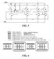
- FIG. 3 Basic netlist for the DICE latch cell (prior art [Nic05]) with nodes 1-4.
- p1-p4 and n1-n4 are the pMOSFET drains and the nMOSFET drains, respectively.
- ns/ps are the source contacts for the two mosfets who's drains are adjacent.).
- p1-p4 and n1-n4 are the pMOSFET drains and the nMOSFET drains of the 4 main storage nodes, respectively. Any cyclic simultaneous permutation of the n and p nodes will be equivalent (and part of the invention).
- the mosfets can be placed in separate active areas, or the adjacent n and p nodes can be placed in the same active area.
- the MOSFET sources can be placed in the line of the drains or in the direction vertical to the line of the drain nodes.
- the well contacts can be placed on either side only, or also surround the adjacent node pairs.
- the nodes can also be arranged in a different order subject to the following rules: two adjacent n-drains, or two adjacent p-drains are always an odd/even pair (e.g., p1 & p2, or n2 and n3), adjacent n-drain to p-drain are always an odd/odd or and even/even pair (e.g., n2 & p2, or p3 & n1).
- Figure 5 Net-list corresponding to the second preferred arrangement.
- the yellow MOSFET may or may not be included, as long as node 6 is connected to drain 6a in figure 5 , and p1 and 6a are physically separate.
- Figure 6 A second preferred layout arrangement. ns/ps are the source contacts for the two mosfets who's drains are adjacent. Node 6a and 6b are connected. The yellow gate adjacent to node 6a may or may not be included (both variants included in the claims), but p1 and 6a are physically separate.
- the layout derives from the layout in figure 1 , and the same variants w.r.t. node permutations, active, source, and well contact arrangements apply.
- Figure 7 Net-list corresponding to the third preferred arrangement.
- the yellow MOSFET may or may not be included, as long as node 6 is connected to drain 6a in figure 4 , and p1 and 6a are physically separate, and node 7 is connected to drain 7a in figure 4 , and n1 and 7a are physically separate.
- Figure 8 A third preferred layout arrangement. ns/ps are the source contacts for the two mosfets who's drains are adjacent. Node 6a-6b are connected, as are node 7a/7b. The yellow gate adjacent to node 6a and 7a may or may not be included (both variants included in the claims), but the adjacent drain areas are physically separate.
- the layout derives from the layout in figure 1 , and the same variants w.r.t. node permutations, active, source, and well contact arrangements apply.
- Figure 9 Net-list corresponding to the fourth preferred arrangement.
- the yellow MOSFET may or may not be included, as long as node 6 is connected to drain 6a, 7 to 7a, 8 to 8a, and 9 to 9a in figure 8 , and 6a , 7a, 8a , 9a are physically separate from their adjacent main drain node.
- Figure 10 A fourth preferred layout arrangement.
- ns/ps are the source contacts for the two mosfets who's drains are adjacent.
- Node 6a/6b, 7a/7b, 8a/8b, and 9a/9b are connected.
- the yellow gates adjacent to nodes 6a,7a, 8a, 9a may or may not be included (both variants included in the claims), but nodes 6a, 7a, 8a, 9a are physically separate from their adjacent MOSFET drains.
- the layout derives from the layout in figure 1 , and the same variants w.r.t. node permutations, active, source, and well contact arrangements apply.
- the claims also cover the various additional variants where and combination of the extra nodes 6a/6b, 7a/7b, 8a/8b, 9a/9b have been included or omitted.
- Figure 11 Circuit schematic and layout for duplicated latch cells (e.g. for BISER) using placement and sizing to ensure complete hardness against single and multiple node single event effects.
- the primary latch can only be upset when node 1 is HIGH
- the redundant latch can only be upset when node 1 (r) is LOW.
- any single event that affects both latches can only upset one of the two latches in the BISER configuration, and therefore, cannot generate an error.
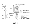
- Figure 12 Example of a duplicated circuit of claim 9 AND 10.
- error signals on both primary and redundant nodes can be generated if both ndrain0 and pdrain1 are affected (if D is high) or if both ndrain1 and pdrain0 are affected (D low).
- This invention comprises a unique new layout method, which takes advantage of the overall circuit response to a single event effect. It also includes specific circuit cells with layout, which have been constructed in accordance with the new layout method.
- a radiation generated single event (soft-) error (SEE) occurs when the charge, generated in the semiconductor material by one or more (e.g. secondary) charged particles, is collected by contact areas.
- the contact areas are the low resistivity regions on, or in, the semiconductor substrate, which are connected to a net in the circuit, e.g., the source and drain areas in a MOSFET technology.
- a circuit net (or node) refers to a part of the circuit, connected by low resistivity regions (metal), which maintains a certain voltage value (referred to as the voltage state of the net) throughout its' extent.
- a net can be connected to any number of contact areas.
- the charge collected by contact areas during a single event leads to current pulses in the circuit, which, in their turn, cause a change in the voltage of the circuit nets, connected to these contact areas, i,e, a voltage pulse in the circuit.
- These pulses can upset a sequential element (latch, flip-flop) or propagate through combinational logic (i.e., a set of digital logic gates) and be latched in as errors at the next sequential element in the circuit.
- a single event can have the effect of increasing the voltage on the net connected to the contact area, or decreasing it, depending on where the contact areas are located in substrate, and how they are connected to the circuit.
- the method in this invention uses an arrangement of contact areas in such a way that single event generated pulses in the circuit, that occur on multiple contact areas, acts to oppose each other, w.r.t. the effects they have on the voltage of the circuit nets, and hence cancel (or greatly reduce the effect of the single event).
- the method also comprises an adjustment the strength of the effect a single event has on the voltage of the circuit nets, when this is desirable to achieve the desired total effect on the circuit.
- This adjustment can be achieved by changing the sizes of the contact areas, and by changing their positions relative to other components in the layout.
- the method can be applied to sequential logic elements (latches, flip-flops, memory cells), to combinational logic (a connection of one or more digital logic gates), or to analog circuit cells.
- the first, section 4.1 uses a placement, and strength adjustment, such that the single event effects, on several contact areas, cancel out each other, in terms of their effect on the circuit nets they are connected to.
- the second, section 4.2 uses a placement, and strength adjustment, such that two, or more, redundant nets in the circuit, are affected differently by a single event, in such a way that a single event cannot simultaneously change their voltage state on several of the redundant nets.
- redundant nets place the contact areas of the redundant nets in a direction, which is such that when the charge from one single event effects both primary, and redundant nets, it is in the direction which is such that it always also affects both opposing nodes in either the primary or the secondary circuit, or that it affects the opposing node of both primary and secondary circuit.
- step one and two above would use the following to characterize the effect of a single event on a source or drain contact area:
- step 3 above would use the following rules for two nodes, each connected to a net carrying redundant signals (primary and secondary nets):
- an alternative to synthesizing a layout where single event effects cancel out each other is to deliberately let one of the contact areas be stronger w.r.t. single event charge collection. This contact area will then always determine the outcome of a single event in on the connected net (e.g., for a p-drain it would always end up HIGH (at Vdd)).
- FIG. 1 shows the schematics of the fundamental components of a latch circuit implemented in a CMOS technology.
- each of the two (main) net is connected to two contacts areas in the layout (the nmos device drain and the pmos drain).
- FIG. 2 shows such an arrangement where we have utilized the first two of the opposing contact area identifications above. We now have a latch which cannot be upset if the single event has such a directions that is passes the two nets of the circuit.
- Step 3 in methodology number 1, as well as method number 2 concerns the case when an additional (redundant) circuit (here a latch) is available.
- an additional (redundant) circuit here a latch
- n1, n2, from the primary latch there will be 4 main nodes, n1, n2, from the primary latch, and n3, n4, from the secondary latch.
- the nodes from one latch will be in opposite states, and, during correct circuit operation, each node in the primary latch will always have the same state as one node in the secondary latch. This situation is shown in table 1, where n1 and n3 maintain the same state, and n2 and n4 maintain the same state.
- step 3 the nodes of the second latch are now placed, w.r.t. the first latch, such that when an extended event occurs that affects both latches, it will be in a direction which affects both opposing nodes in each individual latch, or at least in one of them.
- FIG. 11 shows such an arrangement, where the method with dominating nodes (methodology 2 above) has been used, and the two latches have been placed in such a way relative to each other that at the most, one of the latches can be upset, by any single event, but not both.
- a filtering, or voting circuit is used.
- the filtering ensuring that at any time where one of the redundant nets is wrong (e.g., for the redundant nets carrying the same voltage state; if the voltage states differ) the signal is not allowed to pass through the filtering circuit.
- the Built-In Soft Error (BISER) design [Mitra2005] is an example of such a configuration.
- a voting circuit being used on at least 3 redundant circuit, performs a vote between the voltage states of the redundant nets.
- Triple mode redundancy (TMR) configurations use this type of redundancy.
- This invention also comprises several specific DICE cells, created using the layout method.
- the principal arrangement of the 4 storage nets, of the DICE cells in this inventions, is that the contact areas of the nets are placed along one direction (e.g., figure 4 ), and that they have a certain order, than minimizes or removes the effect of the single event, and hence reduces or removes the possibility that the storage element can be upset by a single event.
- the first variant (variant 1) is shown in figure 4 .
- the MOSFET pairs have been placed in the same active area with a common MOSFET source contact in-between. However, they can also be placed in separate active areas, using separate sources contacts, and they can also be oriented so that the sources are perpendicular to the direction of the drain nodes.
- variants 2-4 ( figure 5-10 ) protective nodes have been added. They act to protect certain sensitive node-pairs and are not (necessarily) active during normal circuit operation. However, they can also be used as active devices connecting their gates to other storage nodes. For example, while variant 1 is much more robust than the normal layout (which does not have other nodes in between the sensitive node pairs), there are still some single event sensitivity remaining, the main being for the node pair p1-n2. By extending variant one as shown in figures 5-6 , the node pair p1-n2 is also protected. This is variant 2. The most sensitive node pair in variant 2 is the n1-p4 node pair, this pair is protected with the extension in variant 3 ( figures 7-8 ). Finally the latch can be made symmetric by adding additional protective nodes. A fully symmetric arrangement of protective nodes is shown in figures 9-10 (third variant).
- additional protective MOSFETs has a general application to circuits which uses redundant nets.
- they can be used to keep the state of a circuit node which becomes floating (not connected to the power, i.e., to VSS or VDD) during a single event.
- Floating nets become very sensitive to the single event charge, their voltage state can change very easily (i.e., even by very weak interaction with the single event).
- the additional protective devices even if they just turn on partially during the single event, will make the nodes, that become floating during a single event, much more stable.
- Another (not DICE) example of the addition of such protective devices for a c-element filtering circuit is shown in figure 13 .
- the invention also comprises a combinational circuit where all, or some of the nets have been duplicated, in such a way that there is one (primary) net that carries the signal, and a second (redundant) net carries the inverse of the signal on the primary net (i.e., when the voltage on the primary net is high, the voltage on the redundant net is always low, and vice versa), and where, in accordance with the layout method, the contact areas of the primary and redundant net, are placed in such a way that when a single event affects both nets, a voltage pulse can only be generated on one of the nets, but not on both.
Abstract
Description
- This invention comprises a layout method to effectively protect logic circuits against soft errors (non-destructive errors) and circuit cells, with layout, which are protected against soft errors. In particular, the method protects against cases where multiple nodes in circuit are affected by a single event. These events lead to multiple errors in the circuit, and while several methods exist to deal with single node errors, multiple node errors are very hard to deal with using any currently existing protection methods. The method is particularly useful for CMOS based logic circuits in modem technologies (≤ 90 nm), where the occurrence of multiple node pulses becomes high (due to the high integration level). It uses a unique layout configuration, which makes the circuits protected against single event generated soft-errors.
- The problem of soft errors generated by single event transients (and single event upsets) is expected to increase drastically in ultra-deep submicron (< 90 nm) technologies. Of particular significance is that logic circuits are expected to become much more sensitive to radiation generated soft-errors and possibly surpass memory as the major source of single event errors. Furthermore, the generation rate of multiple errors, multiple bit upsets (MBU), single-event multiple upset (SEMU) increases.
- The main reason for this is that, with a higher feature integration and higher frequencies, the spatial distribution and pulse length of a single event transient (SET) becomes relatively larger, increasing the probability that an SET pulse is latched-in as a (soft-) error, or that SET pulses are generated simultaneously on several circuit nodes by one single event.
- The problem with increasing soft-error rates is further complicated by the escalating cost of semiconductor design and manufacturing. The high cost involved in developing and maintaining a semiconductor FAB makes it highly desirable to use standard commercial semiconductor manufacturing also for applications that require a high radiation tolerance. Hence, there is a strong drive to develop efficient and robust radhard-by-design (RHBD) techniques for these applications.
- Furthermore, the design process is also becoming very complex and expensive, and it would be highly desirable to be able to re-use standard design IP and libraries as much as possible for radhard applications.
- Current radhard-by-design technology for single event errors include triplication (triple mode redundancy, TMR) or duplication (e.g., built-in soft-error resilience, BiSER). These circuits carry two or more redundant copies of a signal, and use some form of voting, or filtering, circuitry to determine the correct signal among the redundant signals. Filtering preventing a signal to pass in the case that one of the redundant signals is wrong (by comparing the value of the redundant signals), and voting circuits selects the correct signal from the majority among several (3 or more) redundant signals.
- These techniques generate undesirable power and area overhead, and current versions of these techniques cannot handle MBUs or SEMUs. Error correction codes, ECC, for memory, which also (loosely) could be classified as RHBD, is more efficient than duplication/triplication and can, with additional overhead, handle multiple errors in memory circuitry. However, the application of a corresponding error correction to logic circuits is very limited and application specific (e.g., selective parity check or insertion of specialized checking circuit IP).
- State-of-the art for layout techniques for soft-error hard design mainly consist of simple spacing and sizing, and in adding additional contacts.
- A radiation generated single event (soft-) error (SEE) occurs when the charge, generated in the semiconductor material by one or more (e.g. secondary) charge particles, is collected by contact areas on the semiconductor substrate. This leads to current pulses on the circuit nets, connected to these contact areas, which, in their turn, cause voltage pulses in the circuit which can upset a sequential element (latch, flip-flop) or propagate through combinational logic and be latched in as errors at the next sequential element in the circuit.
- This invention comprises a unique new layout method, which takes advantage of the overall circuit response to a single event effect, and, furthermore, comprises circuit cells, with layout, which are protected against soft errors. The method uses an arrangement of critical contact areas in such a way that single event pulses in the circuit, that are generated on multiple nodes, act to oppose each other and hence cancel (or greatly reduce the effect of the single event). In the case that a primary and secondary circuit is used to maintain, or process the signal in a circuit, addition rules, described in
section 4, are used, so that no possibility remains that a error is generated in both primary and secondary circuit, and hence that the combination of primary and secondary circuit will be fully error free. - Table 1. The state for the nodes in a circuit that uses a primary (nodes n1,n2) and secondary (nodes n3,n4) circuit for storage or processing of the state.
-
Figure 1 . Primary opposing nodes in a latch cell. -
Figure 2 . A principal arrangement of opposing node of a latch circuit. -
Figure 3 . Basic netlist for the DICE latch cell (prior art [Nic05]) with nodes 1-4. p1-p4 and n1-n4 are the pMOSFET drains and the nMOSFET drains, respectively. -
Figure 4 . A first preferred layout arrangement for the layout of the DICE latch cell. ns/ps are the source contacts for the two mosfets who's drains are adjacent.). p1-p4 and n1-n4 are the pMOSFET drains and the nMOSFET drains of the 4 main storage nodes, respectively. Any cyclic simultaneous permutation of the n and p nodes will be equivalent (and part of the invention). The mosfets can be placed in separate active areas, or the adjacent n and p nodes can be placed in the same active area. The MOSFET sources can be placed in the line of the drains or in the direction vertical to the line of the drain nodes. The well contacts can be placed on either side only, or also surround the adjacent node pairs. The nodes can also be arranged in a different order subject to the following rules: two adjacent n-drains, or two adjacent p-drains are always an odd/even pair (e.g., p1 & p2, or n2 and n3), adjacent n-drain to p-drain are always an odd/odd or and even/even pair (e.g., n2 & p2, or p3 & n1). -
Figure 5 . Net-list corresponding to the second preferred arrangement. The yellow MOSFET may or may not be included, as long as node 6 is connected todrain 6a infigure 5 , and p1 and 6a are physically separate. -
Figure 6 . A second preferred layout arrangement. ns/ps are the source contacts for the two mosfets who's drains are adjacent. Node 6a and 6b are connected. The yellow gate adjacent tonode 6a may or may not be included (both variants included in the claims), but p1 and 6a are physically separate. The layout derives from the layout infigure 1 , and the same variants w.r.t. node permutations, active, source, and well contact arrangements apply. -
Figure 7 . Net-list corresponding to the third preferred arrangement. The yellow MOSFET may or may not be included, as long as node 6 is connected todrain 6a infigure 4 , and p1 and 6a are physically separate, and node 7 is connected todrain 7a infigure 4 , and n1 and 7a are physically separate. -
Figure 8 . A third preferred layout arrangement. ns/ps are the source contacts for the two mosfets who's drains are adjacent.Node 6a-6b are connected, as arenode 7a/7b. The yellow gate adjacent tonode figure 1 , and the same variants w.r.t. node permutations, active, source, and well contact arrangements apply. -
Figure 9 . Net-list corresponding to the fourth preferred arrangement. The yellow MOSFET may or may not be included, as long as node 6 is connected to drain 6a, 7 to 7a, 8 to 8a, and 9 to 9a infigure 8 , and6a ,7a, 8a ,9a are physically separate from their adjacent main drain node. -
Figure 10 . A fourth preferred layout arrangement. ns/ps are the source contacts for the two mosfets who's drains are adjacent.Node 6a/6b, 7a/7b, 8a/8b, and 9a/9b are connected. The yellow gates adjacent tonodes nodes figure 1 , and the same variants w.r.t. node permutations, active, source, and well contact arrangements apply. Naturally the claims also cover the various additional variants where and combination of theextra nodes 6a/6b, 7a/7b, 8a/8b, 9a/9b have been included or omitted. -
Figure 11 . Circuit schematic and layout for duplicated latch cells (e.g. for BISER) using placement and sizing to ensure complete hardness against single and multiple node single event effects. For a single event affecting several nodes, the primary latch can only be upset whennode 1 is HIGH, and the redundant latch can only be upset when node 1 (r) is LOW. Hence, any single event that affects both latches, can only upset one of the two latches in the BISER configuration, and therefore, cannot generate an error. -
Figure 12 . Example of a duplicated circuit of claim 9 AND 10. In a duplicated inverter where the redundant and primary nodes carry opposite states, error signals on both primary and redundant nodes can be generated if both ndrain0 and pdrain1 are affected (if D is high) or if both ndrain1 and pdrain0 are affected (D low). By placing the nodes such, that if a particle trace goes through two nodes that can cause an error transient on both primary and redundant output, then the trace also passes through the other nodes and the pulse on one of the nets are suppressed. For example, consider the trace in the figure; if node 0 is high, the charge collected on ndrain0 will pull node 0 low (error transient), the charge collected on node pdrain1 will pullnode 1 high, however, the charge collected on node ndrain1 will pullnode 1 low, opposing the effect on pdrain1, and keepingnode 1 low (i.e., preventing the transient on node 1). If node 0 is low, the charge collected on node ndrain1, will pullnode 1 low (error transient), however, the charge collected at ndrain0, will keep node 0 low (i.e., preventing a transient on node 0). If should be pointed out that in the general case there will be some pulses on all nodes, but that it will always hold true that a full swing pulse (a transient that can propagate) only can be generated on one, and one only, of the duplicated nodes. - This invention comprises a unique new layout method, which takes advantage of the overall circuit response to a single event effect. It also includes specific circuit cells with layout, which have been constructed in accordance with the new layout method.
- A radiation generated single event (soft-) error (SEE) occurs when the charge, generated in the semiconductor material by one or more (e.g. secondary) charged particles, is collected by contact areas. The contact areas are the low resistivity regions on, or in, the semiconductor substrate, which are connected to a net in the circuit, e.g., the source and drain areas in a MOSFET technology. A circuit net (or node) refers to a part of the circuit, connected by low resistivity regions (metal), which maintains a certain voltage value (referred to as the voltage state of the net) throughout its' extent. A net can be connected to any number of contact areas.
- The charge collected by contact areas during a single event, leads to current pulses in the circuit, which, in their turn, cause a change in the voltage of the circuit nets, connected to these contact areas, i,e, a voltage pulse in the circuit. These pulses can upset a sequential element (latch, flip-flop) or propagate through combinational logic (i.e., a set of digital logic gates) and be latched in as errors at the next sequential element in the circuit.
- The effect of a single event on the voltage on the circuit net, is different for different contact areas, e.g., a single event can have the effect of increasing the voltage on the net connected to the contact area, or decreasing it, depending on where the contact areas are located in substrate, and how they are connected to the circuit. The method in this invention uses an arrangement of contact areas in such a way that single event generated pulses in the circuit, that occur on multiple contact areas, acts to oppose each other, w.r.t. the effects they have on the voltage of the circuit nets, and hence cancel (or greatly reduce the effect of the single event).
- The method also comprises an adjustment the strength of the effect a single event has on the voltage of the circuit nets, when this is desirable to achieve the desired total effect on the circuit. This adjustment can be achieved by changing the sizes of the contact areas, and by changing their positions relative to other components in the layout.
- The method can be applied to sequential logic elements (latches, flip-flops, memory cells), to combinational logic (a connection of one or more digital logic gates), or to analog circuit cells.
- In the following two section details of two specific ways to apply the method are described. The first, section 4.1, uses a placement, and strength adjustment, such that the single event effects, on several contact areas, cancel out each other, in terms of their effect on the circuit nets they are connected to. The second, section 4.2, uses a placement, and strength adjustment, such that two, or more, redundant nets in the circuit, are affected differently by a single event, in such a way that a single event cannot simultaneously change their voltage state on several of the redundant nets.
- The key steps in method one of the invention are:
- 1. Identify which contact areas have opposing effects on the circuit nets when they are simultaneously affected by a single event
- 2. Place these nodes in the layout next to each other, and in a fully symmetric way with respect to other adjacent contact areas
- a. In particular in a CMOS technology the contact are configured in a symmetric (equivalent) position w.r.t. well junctions and well contacts
- b. If the two contact areas are part of a sequential element (e.g., a latch), this arrangement ensures that these two nodes cannot be upset by a single event that affects both areas, i.e., an event which has an extended charge (e.g., as generated by a charged particle passing through) which is in such a direction that it affects both these nodes.
- c. If nodes are part of a combinational element, the arrangement ensures that the generated output pulse is greatly suppressed, when the generation single event affects both nodes, i.e., an event which has an extended charge (e.g., as generated by a charged particle passing through) which is in such a direction that it affects both these nodes.
- 3. In an element using additional protective circuitry (redundant nets), place the contact areas of the redundant nets in a direction, which is such that when the charge from one single event effects both primary, and redundant nets, it is in the direction which is such that it always also affects both opposing nodes in either the primary or the secondary circuit, or that it affects the opposing node of both primary and secondary circuit.
- Specifically for CMOS technology, step one and two above would use the following to characterize the effect of a single event on a source or drain contact area:
- a. When an n-drain (or source) is affected by a single event, the effect of the single event is to reduce the voltage on the net connected to this contact area, i.e., if the node is high is will tend to switch the voltage, when the node is low, it will not tend to switch the voltage.
- b. When an n-drain (or source) is affected by a single event, the effect of the single event is to reduce the voltage on the net connected to this contact area, i.e., if the node is high is will tend to switch the voltage, when the node is low, it will not tend to switch the voltage.
- Also, specifically for a CMOS technology,
step 3 above, would use the following rules for two nodes, each connected to a net carrying redundant signals (primary and secondary nets): - a. When two n-drains (or sources), one connected to the primary net and one to the secondary net, are affected by a single event, and they always have opposite voltage states, then only one of the primary/secondary nets can be upset (i.e., change its' voltage).
- b. When two p-drains (or sources), one connected to the primary and one to the secondary net, are affected by a single event, and they always have opposite voltage states, then only one of the primary/secondary circuits can be upset.
- c. When an n-drain (or source) from one net, and a p-drain (or source) from the other net is affected, are affected by a single event, and the nets connected to these drains (sources) always have the same voltage state, then only one of the primary/secondary nets can be upset.
- For the case of an element that uses primary and redundant nets to store the state (i.e., the voltage or signal), an alternative to synthesizing a layout where single event effects cancel out each other, is to deliberately let one of the contact areas be stronger w.r.t. single event charge collection. This contact area will then always determine the outcome of a single event in on the connected net (e.g., for a p-drain it would always end up HIGH (at Vdd)). When there are four nets that store the state (2 primary nets, two redundant nets), and we make sure that net connected to the contact areas that is made dominant in the primary circuit part, stores the opposite state to the net connected to the contact area that is made dominant in the redundant circuit part, then only one of the two redundant circuit parts can be upset by an event that affects both circuit parts. Using this variant, the robust cell synthesis methodology would be as follows:
- For designs that use primary and redundant nets to store a state:
- a. Identify which contact areas have opposing circuit effects when they are simultaneously affected by a single event (in the primary as well as the redundant part)
- b. Place these nodes in the layout next to each other, and make one of the nodes dominant w. r. t. a single event (e.g., by making the drain area larger, and changing the distance to the well-junction and the well-ties).
- c. Make sure that the net connected to the dominant contact area of the primary circuit part, stores the opposite state to the net connected to the dominant contact area in the redundant circuit part.
- d. Place the primary and redundant contact areas, relative to each other, in such a way that a single event the affects both the primary and redundant circuitry, also always affects both the dominant and the non-dominant nodes in the primary and in the redundant part.
- (i) In this way, either the primary or the redundant part will be in a state where the dominant node will make sure this circuit part cannot be upset (i.e. change its state or voltage). Hence, in any situation only ONE of the redundant parts can be upset by a single event.
- In a basic sequential logic circuit element (latch, sram-type memory cell, etc.) there are two main nets that maintain the state. These will always have opposite state (voltage).
FIG. 1 shows the schematics of the fundamental components of a latch circuit implemented in a CMOS technology. In this latch, each of the two (main) net is connected to two contacts areas in the layout (the nmos device drain and the pmos drain). - In this configuration the contact areas that will have opposing effects with respect to the state of the latch, when affected by the same single event, can be identified as (
step 1 above): - a. A single event that affects both pmos drains will have opposing effects on the state of the latch
- b. A single event that affects both nmos drains will have opposing effect on the state of the latch
- b. A single event that affects both nmos and pmos drain of the same node will have opposing effect on the state of the latch
- In the symmetric method, we arrange the layout such that drains, with opposing effects, are placed next to each other, in a symmetric arrangement (i.e. w.r.t. symmetric w.r.t the surrounding layout, and having the same shape). This is
step 2 in themethodology number 1 above.FIG. 2 shows such an arrangement where we have utilized the first two of the opposing contact area identifications above. We now have a latch which cannot be upset if the single event has such a directions that is passes the two nets of the circuit. -
Step 3 inmethodology number 1, as well asmethod number 2, concerns the case when an additional (redundant) circuit (here a latch) is available. In a circuit configuration that uses two latches to maintain the states, there will be 4 main nodes, n1, n2, from the primary latch, and n3, n4, from the secondary latch. The nodes from one latch will be in opposite states, and, during correct circuit operation, each node in the primary latch will always have the same state as one node in the secondary latch. This situation is shown in table 1, where n1 and n3 maintain the same state, and n2 and n4 maintain the same state. - According to
step 3, the nodes of the second latch are now placed, w.r.t. the first latch, such that when an extended event occurs that affects both latches, it will be in a direction which affects both opposing nodes in each individual latch, or at least in one of them.FIG. 11 shows such an arrangement, where the method with dominating nodes (methodology 2 above) has been used, and the two latches have been placed in such a way relative to each other that at the most, one of the latches can be upset, by any single event, but not both. - The same situation is the same also for other sequential elements (e.g., memory cells) and the method applies to these elements as well. The method also applies to elements which uses more than 2 nodes to maintain the state, as well as non-sequential elements with a primary and secondary redundant net.
Table 1. The state for the nodes in a circuit that uses a primary (nodes n1,n2) and secondary (nodes n3, n4) circuit for storage or processing of the state. Node: n1 n2 n3 n4 State 0 0 1 0 1 State 11 0 1 0 - To extract the correct signal from the two, or more, redundant nets, a filtering, or voting circuit is used. The filtering ensuring that at any time where one of the redundant nets is wrong (e.g., for the redundant nets carrying the same voltage state; if the voltage states differ) the signal is not allowed to pass through the filtering circuit. The Built-In Soft Error (BISER) design [Mitra2005] is an example of such a configuration. A voting circuit, being used on at least 3 redundant circuit, performs a vote between the voltage states of the redundant nets. Triple mode redundancy (TMR) configurations use this type of redundancy.
- This invention also comprises several specific DICE cells, created using the layout method. The DICE (Dual Interlocked Cell) latch [Nic2005], the circuit of which is shown in
figure 3 , also uses four nets to store the circuit state, but as can be seen infigure 3 , they are not connected as two separate latches, but in an interlocked way. - The principal arrangement of the 4 storage nets, of the DICE cells in this inventions, is that the contact areas of the nets are placed along one direction (e.g.,
figure 4 ), and that they have a certain order, than minimizes or removes the effect of the single event, and hence reduces or removes the possibility that the storage element can be upset by a single event. The first variant (variant 1) is shown infigure 4 . In this variant the MOSFET pairs have been placed in the same active area with a common MOSFET source contact in-between. However, they can also be placed in separate active areas, using separate sources contacts, and they can also be oriented so that the sources are perpendicular to the direction of the drain nodes. - In variants 2-4 (
figure 5-10 ) protective nodes have been added. They act to protect certain sensitive node-pairs and are not (necessarily) active during normal circuit operation. However, they can also be used as active devices connecting their gates to other storage nodes. For example, whilevariant 1 is much more robust than the normal layout (which does not have other nodes in between the sensitive node pairs), there are still some single event sensitivity remaining, the main being for the node pair p1-n2. By extending variant one as shown infigures 5-6 , the node pair p1-n2 is also protected. This isvariant 2. The most sensitive node pair invariant 2 is the n1-p4 node pair, this pair is protected with the extension in variant 3 (figures 7-8 ). Finally the latch can be made symmetric by adding additional protective nodes. A fully symmetric arrangement of protective nodes is shown infigures 9-10 (third variant). - The addition of additional protective MOSFETs has a general application to circuits which uses redundant nets. In the same way as in the case of the DICE circuit, they can be used to keep the state of a circuit node which becomes floating (not connected to the power, i.e., to VSS or VDD) during a single event. Floating nets become very sensitive to the single event charge, their voltage state can change very easily (i.e., even by very weak interaction with the single event). The additional protective devices, even if they just turn on partially during the single event, will make the nodes, that become floating during a single event, much more stable. Another (not DICE) example of the addition of such protective devices for a c-element filtering circuit is shown in
figure 13 . - The invention also comprises a combinational circuit where all, or some of the nets have been duplicated, in such a way that there is one (primary) net that carries the signal, and a second (redundant) net carries the inverse of the signal on the primary net (i.e., when the voltage on the primary net is high, the voltage on the redundant net is always low, and vice versa), and where, in accordance with the layout method, the contact areas of the primary and redundant net, are placed in such a way that when a single event affects both nets, a voltage pulse can only be generated on one of the nets, but not on both. For this type of duplicated combinational circuit, a filtering also needs to be applied to the outputs (at some point before the signal is latched into a single sequential element), which prevents propagation of a signal, unless both nets have their correct state (i.e., one being the inverse of the other). Alternatively sequential elements can also be duplicated, and an error detection and correction added at some point in the circuit (an error being identified by comparing the signal on the two redundant nets). This type of duplicated combinational circuit is shown in
figure 12 .
Claims (5)
- A sequential logic or memory cell and layout, which uses two or more latches to store the state of the element, each latch having at least one net that stores the voltage state and at least one net that stores the opposite value (inverse) of the voltage state, comprising:a. an arrangement of the contact areas of each net (which keep a certain voltage state or its' inverse), in the such a way that the contacts areas of at least 4 of these nets are positioned symmetrically along one line in the layout, and positioned relative to each other such that no two contact areas, which:i. carry the same voltage state, and for which a single event have the same effect on the voltage state of the net; orii. carry different voltage states (i.e., a certain state and its' inverse), and for which a single event have opposite effect on the data (voltage) of the net are placed next to each other.
- The sequential logic or memory cell and layout of claim 1, wherein a filtering or voting circuit is connected to the output of redundant nets, said filtering circuit, being used in the case of two redundant nets, preventing a data signal to pass unless both nets have the correct data, said voting circuit used on three redundant nets, performing a vote between the states of the redundant nets, comprising:a. a layout where the strength of the response to a single event have been adjusted such that the total effect, caused by a single event, on one of the nets (primary) is opposite to the total effect, caused by a single event, on its' redundant counterpart, ensuring that when a single event affects both the primary and redundant nets, one and only one, of these nets can change its state.
- A combinational circuit, where logic element have been duplicated (either throughout or in selected parts) and hence the data signal is carried by a primary net, and by a secondary net (carrying either the signal or it's inverse), and where either filtering circuits, preventing a signal to pass unless the two redundant nets carry the correct signal, have been place in front of each sequential elements, or the sequential elements also have been duplicated (the latter case requiring an error detection and/or correction at the end of the duplicated circuit chain), comprising:a. a layout where the contacts areas of two redundant nets (primary and secondary) are placed such that there is no straight line between a first and a second contact area, each from separate redundant nets, ad for which a single event has the effect of changing the voltage state in the net connected to the circuit area, unless there is, along this line, in between the first and second contact area, at least one third contacts area, for which a single event has an opposite effect, to that of the first and second contact areas, on the voltage state of at least one of the two redundant nets.
- The combinational circuit of claim 3 comprising:a. a layout where the strength of the response to a single event have been adjusted such that the total effect, caused by a single event, on one of two redundant nets is opposite to the total effect, caused by a single event, on the other of the two redundant nets, ensuring that when a single event affects both of the two redundant nets, only one of these two nets can generate and error signal in the circuit.
- A processor readable medium comprising executable instructions that implements the methodology of any one of claims 1-4.
Applications Claiming Priority (5)
| Application Number | Priority Date | Filing Date | Title |
|---|---|---|---|
| US1159908P | 2008-01-17 | 2008-01-17 | |
| US1198908P | 2008-01-22 | 2008-01-22 | |
| US6848308P | 2008-03-07 | 2008-03-07 | |
| US12300308P | 2008-04-05 | 2008-04-05 | |
| EP09702623.1A EP2245740B8 (en) | 2008-01-17 | 2009-01-15 | Layout method for soft-error hard electronics, and radiation hardened logic cell |
Related Parent Applications (2)
| Application Number | Title | Priority Date | Filing Date |
|---|---|---|---|
| EP09702623.1A Division EP2245740B8 (en) | 2008-01-17 | 2009-01-15 | Layout method for soft-error hard electronics, and radiation hardened logic cell |
| EP09702623.1A Division-Into EP2245740B8 (en) | 2008-01-17 | 2009-01-15 | Layout method for soft-error hard electronics, and radiation hardened logic cell |
Publications (2)
| Publication Number | Publication Date |
|---|---|
| EP2685633A2 true EP2685633A2 (en) | 2014-01-15 |
| EP2685633A3 EP2685633A3 (en) | 2014-05-07 |
Family
ID=40875970
Family Applications (2)
| Application Number | Title | Priority Date | Filing Date |
|---|---|---|---|
| EP09702623.1A Not-in-force EP2245740B8 (en) | 2008-01-17 | 2009-01-15 | Layout method for soft-error hard electronics, and radiation hardened logic cell |
| EP13176436.7A Withdrawn EP2685633A3 (en) | 2008-01-17 | 2009-01-15 | Layout method for soft-error hard electronics, and radiation hardened logic cell |
Family Applications Before (1)
| Application Number | Title | Priority Date | Filing Date |
|---|---|---|---|
| EP09702623.1A Not-in-force EP2245740B8 (en) | 2008-01-17 | 2009-01-15 | Layout method for soft-error hard electronics, and radiation hardened logic cell |
Country Status (6)
| Country | Link |
|---|---|
| US (3) | US20090184733A1 (en) |
| EP (2) | EP2245740B8 (en) |
| JP (3) | JP2011512026A (en) |
| KR (1) | KR20100138874A (en) |
| CN (1) | CN101919162B (en) |
| WO (1) | WO2009091928A2 (en) |
Families Citing this family (31)
| Publication number | Priority date | Publication date | Assignee | Title |
|---|---|---|---|---|
| EP2245740B8 (en) | 2008-01-17 | 2014-10-01 | Klas Olof Lilja | Layout method for soft-error hard electronics, and radiation hardened logic cell |
| US8495550B2 (en) * | 2009-01-15 | 2013-07-23 | Klas Olof Lilja | Soft error hard electronic circuit and layout |
| US20140157223A1 (en) * | 2008-01-17 | 2014-06-05 | Klas Olof Lilja | Circuit and layout design methods and logic cells for soft error hard integrated circuits |
| US8217458B2 (en) * | 2009-12-11 | 2012-07-10 | Honeywell International Inc. | Non-aligned antenna effect protection circuit with single event transient hardness |
| US8418106B2 (en) * | 2010-08-31 | 2013-04-09 | International Business Machines Corporation | Techniques for employing retiming and transient simplification on netlists that include memory arrays |
| US8739010B2 (en) * | 2010-11-19 | 2014-05-27 | Altera Corporation | Memory array with redundant bits and memory element voting circuits |
| US9041429B2 (en) | 2011-06-02 | 2015-05-26 | Arizona Board Of Regents, A Body Corporate Of The State Of Arizona, Acting For And On Behalf Of Arizona State University | Sequential state elements for triple-mode redundant state machines, related methods, and systems |
| US8791718B2 (en) * | 2011-06-02 | 2014-07-29 | Arizona Board Of Regents For And On Behalf Of Arizona State University | Sequential state elements in triple-mode redundant (TMR) state machines |
| CN102314538B (en) * | 2011-09-20 | 2013-04-17 | 中国科学院微电子研究所 | Method for layout of transistors of fault-tolerance storage unit |
| WO2013082611A2 (en) * | 2011-12-02 | 2013-06-06 | Robust Chip Inc. | Soft error hard electronics layout arrangement and logic cells |
| US9058853B2 (en) * | 2012-08-16 | 2015-06-16 | Xilinx, Inc. | Integrated circuit having improved radiation immunity |
| US9054688B2 (en) | 2012-09-19 | 2015-06-09 | Arizona Board Of Regents, A Body Corporate Of The State Of Arizona, Acting For And On Behalf Of Arizona State University | Sequential state elements radiation hardened by design |
| WO2014066402A1 (en) * | 2012-10-22 | 2014-05-01 | Klas Olof Lilja | Circuit and layout design methods and logic cells for soft error hard integrated circuits |
| CN103077739B (en) * | 2012-12-31 | 2015-07-29 | 清华大学 | A kind of redundancy structure dynamic random-access storage unit |
| KR102314540B1 (en) * | 2013-09-20 | 2021-10-19 | 어드밴스드 테크놀러지 머티리얼즈, 인코포레이티드 | Apparatus and method for pressure dispensing of high viscosity liquid-containing materials |
| US9569583B2 (en) * | 2014-04-07 | 2017-02-14 | TallannQuest LLC | Method and system for computer-aided design of radiation-hardened integrated circuits |
| CN103955571B (en) * | 2014-04-22 | 2017-07-28 | 北京控制工程研究所 | A kind of soft error injection and verification method for Flouride-resistani acid phesphatase chip |
| US9734272B2 (en) | 2014-06-13 | 2017-08-15 | Arizona Board Of Regents On Behalf Of Arizona State University | Techniques for generating physical layouts of in silico multi mode integrated circuits |
| KR20160010166A (en) * | 2014-07-18 | 2016-01-27 | 에스케이하이닉스 주식회사 | Integrated circuit |
| CN105609504B (en) * | 2015-12-25 | 2018-11-06 | 北京时代民芯科技有限公司 | A kind of anti-SEU multiple node upsets storage unit domain structure of trap isolated form |
| US10579536B2 (en) | 2016-08-09 | 2020-03-03 | Arizona Board Of Regents On Behalf Of Arizona State University | Multi-mode radiation hardened multi-core microprocessors |
| KR102567233B1 (en) * | 2016-11-08 | 2023-08-17 | 에스케이하이닉스 주식회사 | Semiconductor device having dice latches |
| CN106876383B (en) * | 2017-01-03 | 2019-08-09 | 中国人民解放军国防科学技术大学 | It is a kind of for bombardment single-ion transient state reinforcement means of the NMOS transistor without area overhead |
| CN106788380B (en) * | 2017-01-12 | 2020-03-24 | 深圳大学 | Asynchronous set D trigger resistant to single event upset |
| US11374567B2 (en) * | 2017-02-11 | 2022-06-28 | Klas Olof Lilja | Circuit for low power, radiation hard logic cell |
| CN110741551B (en) * | 2017-06-15 | 2021-12-24 | 卓思私人有限公司 | Circuit and method of forming a circuit |
| KR101984109B1 (en) * | 2017-11-22 | 2019-09-03 | 한국원자력연구원 | Logic cell formed of a radiant mosfet(metal oxide semiconductor field effect transistor) |
| US10558775B2 (en) | 2017-12-20 | 2020-02-11 | International Business Machines Corporation | Memory element graph-based placement in integrated circuit design |
| US11069683B2 (en) * | 2018-10-05 | 2021-07-20 | Ics Llc | Self restoring logic structures |
| US11030367B2 (en) | 2019-09-11 | 2021-06-08 | International Business Machines Corporation | Out-of-context feedback hierarchical large block synthesis (HLBS) optimization |
| JPWO2021059582A1 (en) | 2019-09-27 | 2021-04-01 |
Family Cites Families (74)
| Publication number | Priority date | Publication date | Assignee | Title |
|---|---|---|---|---|
| US5065048A (en) | 1988-09-19 | 1991-11-12 | Hitachi, Ltd. | Semiconductor logic circuit with noise suppression circuit |
| JP2859288B2 (en) * | 1989-03-20 | 1999-02-17 | 株式会社日立製作所 | Semiconductor integrated circuit device and method of manufacturing the same |
| US5111429A (en) * | 1990-11-06 | 1992-05-05 | Idaho Research Foundation, Inc. | Single event upset hardening CMOS memory circuit |
| CN2218426Y (en) * | 1994-06-16 | 1996-01-24 | 东南大学 | High performance hybrid integrated optic trunker |
| JP2778550B2 (en) * | 1995-09-08 | 1998-07-23 | 日本電気株式会社 | Method for manufacturing semiconductor integrated circuit |
| US5870332A (en) | 1996-04-22 | 1999-02-09 | United Technologies Corporation | High reliability logic circuit for radiation environment |
| US5898711A (en) * | 1997-05-15 | 1999-04-27 | Vlsi Technology, Inc. | Single event upset detection and protection in an integrated circuit |
| US6127864A (en) * | 1998-08-19 | 2000-10-03 | Mission Research Corporation | Temporally redundant latch for preventing single event disruptions in sequential integrated circuits |
| US6326809B1 (en) | 1999-09-27 | 2001-12-04 | University Of New Mexico | Apparatus for and method of eliminating single event upsets in combinational logic |
| US6278287B1 (en) * | 1999-10-27 | 2001-08-21 | The Boeing Company | Isolated well transistor structure for mitigation of single event upsets |
| US6433983B1 (en) * | 1999-11-24 | 2002-08-13 | Honeywell Inc. | High performance output buffer with ESD protection |
| US6573773B2 (en) | 2000-02-04 | 2003-06-03 | University Of New Mexico | Conflict free radiation tolerant storage cell |
| US6614257B2 (en) * | 2000-05-12 | 2003-09-02 | Bae Systems Information And Electronics Systems Integration, Inc. | Logic architecture for single event upset immunity |
| US7036059B1 (en) * | 2001-02-14 | 2006-04-25 | Xilinx, Inc. | Techniques for mitigating, detecting and correcting single event upset effects in systems using SRAM-based field programmable gate arrays |
| US6549443B1 (en) * | 2001-05-16 | 2003-04-15 | Rockwell Collins, Inc. | Single event upset resistant semiconductor circuit element |
| JP2002373899A (en) | 2001-06-13 | 2002-12-26 | Denso Corp | Method for simulating characteristics of semiconductor device |
| JP2003173681A (en) | 2001-12-07 | 2003-06-20 | Mitsubishi Electric Corp | Semiconductor memory circuit and latch circuit |
| JP3718687B2 (en) * | 2002-07-09 | 2005-11-24 | 独立行政法人 宇宙航空研究開発機構 | Inverter, semiconductor logic circuit, static random access memory, and data latch circuit |
| CN2629309Y (en) * | 2003-06-06 | 2004-07-28 | 戴迪 | Antiinterference protector for electric appliance |
| JP3722225B2 (en) * | 2003-09-01 | 2005-11-30 | セイコーエプソン株式会社 | Semiconductor device and semiconductor memory device using the same |
| US7023235B2 (en) * | 2003-12-12 | 2006-04-04 | Universities Research Association, Inc. | Redundant single event upset supression system |
| EP2107679A3 (en) * | 2004-02-04 | 2010-01-20 | Japan Aerospace Exploration Agency | Single-event-effect tolerant SOI-based logic device |
| US7773442B2 (en) * | 2004-06-25 | 2010-08-10 | Cypress Semiconductor Corporation | Memory cell array latchup prevention |
| US7075337B2 (en) * | 2004-06-30 | 2006-07-11 | Bae Systems Information And Electronic Systems Integration, Inc. | Single event upset immune keeper circuit and method for dual redundant dynamic logic |
| JP4551731B2 (en) * | 2004-10-15 | 2010-09-29 | 株式会社東芝 | Semiconductor integrated circuit |
| US7343579B2 (en) * | 2004-11-30 | 2008-03-11 | Physical Sciences | Reconfigurable environmentally adaptive computing |
| US7215135B2 (en) * | 2004-12-02 | 2007-05-08 | Honeywell International Inc. | Single event upset hardened circuitry without sensitivity to overshoot and/or undershoot conditions |
| US7234121B2 (en) * | 2005-01-06 | 2007-06-19 | Texas Instruments Incorporated | Method of fabricating an integrated circuit to improve soft error performance |
| JP4783022B2 (en) | 2005-01-17 | 2011-09-28 | 株式会社東芝 | Semiconductor integrated circuit device |
| JP2006339355A (en) * | 2005-06-01 | 2006-12-14 | Nec Electronics Corp | Semiconductor integrated circuit device and its designing method |
| US7139190B1 (en) * | 2005-06-14 | 2006-11-21 | Xilinx, Inc. | Single event upset tolerant memory cell layout |
| US20070050740A1 (en) * | 2005-08-29 | 2007-03-01 | Christian Jacobi | Method and System for Performing Functional Formal Verification of Logic Circuits |
| US7236001B2 (en) | 2005-09-02 | 2007-06-26 | Honeywell International Inc. | Redundancy circuits hardened against single event upsets |
| US7358572B2 (en) * | 2005-09-30 | 2008-04-15 | International Business Machines Corporation | Radiation tolerant electrostatic discharge protection networks |
| EP1949425A4 (en) * | 2005-10-14 | 2010-08-18 | Silicon Space Technology Corp | Radiation hardened isolation structures and fabrication methods |
| US7327197B2 (en) | 2005-10-20 | 2008-02-05 | Honeywell International, Inc. | Radiation hardened phase locked loop |
| JP2007124343A (en) * | 2005-10-28 | 2007-05-17 | Toshiba Corp | Data-holding circuit |
| US20070096754A1 (en) * | 2005-11-03 | 2007-05-03 | Honeywell International Inc. | Method and system for analyzing single event upset in semiconductor devices |
| US7679403B2 (en) * | 2005-11-08 | 2010-03-16 | Honeywell International Inc. | Dual redundant dynamic logic |
| US7489538B2 (en) * | 2005-11-14 | 2009-02-10 | University Of Idaho | Radiation tolerant combinational logic cell |
| JP4332652B2 (en) | 2005-12-12 | 2009-09-16 | 独立行政法人 宇宙航空研究開発機構 | Single event resistant latch circuit and flip-flop circuit |
| US7298010B1 (en) * | 2006-02-21 | 2007-11-20 | Sandia Corporation | Radiation-hardened transistor and integrated circuit |
| US8767444B2 (en) * | 2006-03-27 | 2014-07-01 | Honeywell International Inc. | Radiation-hardened memory element with multiple delay elements |
| US8115515B2 (en) * | 2006-03-28 | 2012-02-14 | Honeywell International Inc. | Radiation hardened differential output buffer |
| US7644311B2 (en) * | 2006-03-31 | 2010-01-05 | Integrated Device Technology, Inc. | Logic soft error rate prediction and improvement |
| US7627840B2 (en) * | 2006-07-13 | 2009-12-01 | International Business Machines Corporation | Method for soft error modeling with double current pulse |
| US7864561B2 (en) | 2006-07-28 | 2011-01-04 | Taiwan Semiconductor Manufacturing Co., Ltd. | Cell structure with buried capacitor for soft error rate improvement |
| US7761828B2 (en) | 2006-08-18 | 2010-07-20 | Partition Design, Inc. | Partitioning electronic circuit designs into simulation-ready blocks |
| JP4928878B2 (en) | 2006-09-11 | 2012-05-09 | 株式会社東芝 | Nonvolatile semiconductor memory device |
| US7482842B2 (en) * | 2006-09-15 | 2009-01-27 | International Business Machines Corporation | Radiation hardened phase frequency detector for implementing enhanced radiation immunity performance |
| US7515452B1 (en) * | 2007-01-03 | 2009-04-07 | Xilinx, Inc. | Interleaved memory cell with single-event-upset tolerance |
| US7818702B2 (en) * | 2007-02-28 | 2010-10-19 | International Business Machines Corporation | Structure incorporating latch-up resistant semiconductor device structures on hybrid substrates |
| US7529118B2 (en) * | 2007-03-28 | 2009-05-05 | Intel Corporation | Generalized interlocked register cell (GICE) |
| WO2009038817A2 (en) * | 2007-04-13 | 2009-03-26 | Klas Olof Lilja | Method, and extensions, to couple substrate effects and compact model circuit simulation for efficient simulation of semiconductor devices and circuit |
| US7774732B2 (en) * | 2007-08-14 | 2010-08-10 | International Business Machines Corporation | Method for radiation tolerance by automated placement |
| US8468484B2 (en) | 2008-01-17 | 2013-06-18 | Klas Olof Lilja | Layout method for soft-error hard electronics, and radiation hardened logic cell |
| US8495550B2 (en) * | 2009-01-15 | 2013-07-23 | Klas Olof Lilja | Soft error hard electronic circuit and layout |
| US20130227499A1 (en) | 2008-01-17 | 2013-08-29 | Klas Olof Lilja | Layout method for soft-error hard electronics, and radiation hardened logic cell |
| US20130038348A1 (en) | 2008-01-17 | 2013-02-14 | Klas Olof Lilja | Layout method for soft-error hard electronics, and radiation hardened logic cell |
| US20140157223A1 (en) | 2008-01-17 | 2014-06-05 | Klas Olof Lilja | Circuit and layout design methods and logic cells for soft error hard integrated circuits |
| EP2245740B8 (en) | 2008-01-17 | 2014-10-01 | Klas Olof Lilja | Layout method for soft-error hard electronics, and radiation hardened logic cell |
| US7772874B2 (en) | 2008-01-28 | 2010-08-10 | Actel Corporation | Single event transient mitigation and measurement in integrated circuits |
| US8191021B2 (en) * | 2008-01-28 | 2012-05-29 | Actel Corporation | Single event transient mitigation and measurement in integrated circuits |
| US7907461B1 (en) * | 2008-03-03 | 2011-03-15 | Xilinx, Inc. | Structures and methods of preventing an unintentional state change in a data storage node of a latch |
| US7965540B2 (en) | 2008-03-26 | 2011-06-21 | International Business Machines Corporation | Structure and method for improving storage latch susceptibility to single event upsets |
| US7733144B2 (en) * | 2008-05-29 | 2010-06-08 | International Business Machines Corporation | Radiation hardened CMOS master latch with redundant clock input circuits and design structure therefor |
| US8042071B2 (en) * | 2008-06-30 | 2011-10-18 | Freescale Semiconductor, Inc. | Circuit and method for avoiding soft errors in storage devices |
| US7961501B1 (en) | 2008-07-10 | 2011-06-14 | Ryan Technologies, LLC | Radiation sensors and single-event-effects suppression devices |
| US8054099B2 (en) | 2009-07-29 | 2011-11-08 | The Boeing Company | Method and apparatus for reducing radiation and cross-talk induced data errors |
| US8081010B1 (en) | 2009-11-24 | 2011-12-20 | Ics, Llc | Self restoring logic |
| JP5433437B2 (en) | 2010-01-21 | 2014-03-05 | ルネサスエレクトロニクス株式会社 | Semiconductor integrated circuit device |
| WO2013082611A2 (en) | 2011-12-02 | 2013-06-06 | Robust Chip Inc. | Soft error hard electronics layout arrangement and logic cells |
| WO2014066402A1 (en) | 2012-10-22 | 2014-05-01 | Klas Olof Lilja | Circuit and layout design methods and logic cells for soft error hard integrated circuits |
| US9082624B2 (en) * | 2013-01-02 | 2015-07-14 | International Business Machines Corporation | Signal path of a multiple-patterned semiconductor device |
-
2009
- 2009-01-15 EP EP09702623.1A patent/EP2245740B8/en not_active Not-in-force
- 2009-01-15 EP EP13176436.7A patent/EP2685633A3/en not_active Withdrawn
- 2009-01-15 US US12/354,655 patent/US20090184733A1/en not_active Abandoned
- 2009-01-15 JP JP2010543259A patent/JP2011512026A/en active Pending
- 2009-01-15 CN CN2009801024867A patent/CN101919162B/en active Active
- 2009-01-15 WO PCT/US2009/031160 patent/WO2009091928A2/en active Application Filing
- 2009-01-15 KR KR1020107017290A patent/KR20100138874A/en not_active Application Discontinuation
-
2011
- 2011-10-19 US US13/277,135 patent/US8566770B2/en active Active
-
2013
- 2013-09-13 US US14/026,648 patent/US9081926B2/en active Active
-
2014
- 2014-10-10 JP JP2014208823A patent/JP2015053498A/en active Pending
-
2015
- 2015-07-08 JP JP2015136983A patent/JP2016001741A/en active Pending
Non-Patent Citations (1)
| Title |
|---|
| None |
Also Published As
| Publication number | Publication date |
|---|---|
| US20140019921A1 (en) | 2014-01-16 |
| JP2016001741A (en) | 2016-01-07 |
| WO2009091928A3 (en) | 2009-10-22 |
| JP2015053498A (en) | 2015-03-19 |
| EP2245740A2 (en) | 2010-11-03 |
| US20090184733A1 (en) | 2009-07-23 |
| US20120185816A1 (en) | 2012-07-19 |
| EP2685633A3 (en) | 2014-05-07 |
| CN101919162B (en) | 2013-12-11 |
| CN101919162A (en) | 2010-12-15 |
| EP2245740B8 (en) | 2014-10-01 |
| KR20100138874A (en) | 2010-12-31 |
| EP2245740B1 (en) | 2014-03-12 |
| US9081926B2 (en) | 2015-07-14 |
| JP2011512026A (en) | 2011-04-14 |
| EP2245740A4 (en) | 2013-01-16 |
| US8566770B2 (en) | 2013-10-22 |
| WO2009091928A2 (en) | 2009-07-23 |
Similar Documents
| Publication | Publication Date | Title |
|---|---|---|
| EP2245740B1 (en) | Layout method for soft-error hard electronics, and radiation hardened logic cell | |
| US8468484B2 (en) | Layout method for soft-error hard electronics, and radiation hardened logic cell | |
| US8495550B2 (en) | Soft error hard electronic circuit and layout | |
| US8191021B2 (en) | Single event transient mitigation and measurement in integrated circuits | |
| US20130038348A1 (en) | Layout method for soft-error hard electronics, and radiation hardened logic cell | |
| JP2008522525A (en) | Electronic device having logic circuit and method for designing logic circuit. | |
| Haghi et al. | The 90 nm Double-DICE storage element to reduce Single-Event upsets | |
| Lin et al. | Soft-error hardening designs of nanoscale CMOS latches | |
| Wey et al. | A low power-delay-product and robust Isolated-DICE based SEU-tolerant latch circuit design | |
| Eftaxiopoulos et al. | Low leakage radiation tolerant CAM/TCAM cell | |
| US10181851B2 (en) | Dual interlocked logic circuits | |
| Maharrey et al. | Dual-interlocked logic for single-event transient mitigation | |
| US20130227499A1 (en) | Layout method for soft-error hard electronics, and radiation hardened logic cell | |
| Zorian et al. | Impact of soft error challenge on SoC design | |
| Yazdanshenas et al. | A scalable dependability scheme for routing fabric of SRAM-based reconfigurable devices | |
| Chong et al. | Radiation-Hardened-by-Design (RHBD) Digital Design Approaches: A Case Study on an 8051 Microcontroller | |
| Chang et al. | SERL: Soft error resilient latch design | |
| Katunin et al. | Evaluation Based on TCAD Simulation of a Failure Tolerance of the Elements on the Cells STG DICE for 65-nm CMOS Blocks of an Associative Memory | |
| US7642813B2 (en) | Error correcting logic system | |
| US20220209773A1 (en) | Semiconductor device | |
| Maharrey | Dual interlocked logic: A radiation-hardened-by-design technique for single-event logic errors | |
| Franciscatto et al. | DARE180X: A 0.18 µm mixed-signal radiation-hardened library for low-power applications | |
| He et al. | Evaluating the Practicability of Error-Detection Circuit Exposed to Single-Event Upsets in 65 nm CMOS Technology | |
| Skoufis | Coping with delays and hazards in buses and random logic in deep sub-micron | |
| Devlin et al. | Self Synchronous Circuits for Robust Operation in Low Voltage and Soft Error Prone Environments |
Legal Events
| Date | Code | Title | Description |
|---|---|---|---|
| PUAI | Public reference made under article 153(3) epc to a published international application that has entered the european phase |
Free format text: ORIGINAL CODE: 0009012 |
|
| AC | Divisional application: reference to earlier application |
Ref document number: 2245740 Country of ref document: EP Kind code of ref document: P |
|
| AK | Designated contracting states |
Kind code of ref document: A2 Designated state(s): AT BE BG CH CY CZ DE DK EE ES FI FR GB GR HR HU IE IS IT LI LT LU LV MC MK MT NL NO PL PT RO SE SI SK TR |
|
| PUAL | Search report despatched |
Free format text: ORIGINAL CODE: 0009013 |
|
| AK | Designated contracting states |
Kind code of ref document: A3 Designated state(s): AT BE BG CH CY CZ DE DK EE ES FI FR GB GR HR HU IE IS IT LI LT LU LV MC MK MT NL NO PL PT RO SE SI SK TR |
|
| RIC1 | Information provided on ipc code assigned before grant |
Ipc: H03K 19/003 20060101AFI20140331BHEP |
|
| STAA | Information on the status of an ep patent application or granted ep patent |
Free format text: STATUS: THE APPLICATION IS DEEMED TO BE WITHDRAWN |
|
| 18D | Application deemed to be withdrawn |
Effective date: 20140801 |