EP2685516A1 - Method of manufacturing display panel - Google Patents
Method of manufacturing display panel Download PDFInfo
- Publication number
- EP2685516A1 EP2685516A1 EP20130176241 EP13176241A EP2685516A1 EP 2685516 A1 EP2685516 A1 EP 2685516A1 EP 20130176241 EP20130176241 EP 20130176241 EP 13176241 A EP13176241 A EP 13176241A EP 2685516 A1 EP2685516 A1 EP 2685516A1
- Authority
- EP
- European Patent Office
- Prior art keywords
- layer
- film
- adhesive layer
- display panel
- passivation film
- Prior art date
- Legal status (The legal status is an assumption and is not a legal conclusion. Google has not performed a legal analysis and makes no representation as to the accuracy of the status listed.)
- Granted
Links
Images









Classifications
-
- H—ELECTRICITY
- H01—ELECTRIC ELEMENTS
- H01J—ELECTRIC DISCHARGE TUBES OR DISCHARGE LAMPS
- H01J9/00—Apparatus or processes specially adapted for the manufacture, installation, removal, maintenance of electric discharge tubes, discharge lamps, or parts thereof; Recovery of material from discharge tubes or lamps
-
- G—PHYSICS
- G02—OPTICS
- G02F—OPTICAL DEVICES OR ARRANGEMENTS FOR THE CONTROL OF LIGHT BY MODIFICATION OF THE OPTICAL PROPERTIES OF THE MEDIA OF THE ELEMENTS INVOLVED THEREIN; NON-LINEAR OPTICS; FREQUENCY-CHANGING OF LIGHT; OPTICAL LOGIC ELEMENTS; OPTICAL ANALOGUE/DIGITAL CONVERTERS
- G02F1/00—Devices or arrangements for the control of the intensity, colour, phase, polarisation or direction of light arriving from an independent light source, e.g. switching, gating or modulating; Non-linear optics
- G02F1/01—Devices or arrangements for the control of the intensity, colour, phase, polarisation or direction of light arriving from an independent light source, e.g. switching, gating or modulating; Non-linear optics for the control of the intensity, phase, polarisation or colour
- G02F1/13—Devices or arrangements for the control of the intensity, colour, phase, polarisation or direction of light arriving from an independent light source, e.g. switching, gating or modulating; Non-linear optics for the control of the intensity, phase, polarisation or colour based on liquid crystals, e.g. single liquid crystal display cells
- G02F1/133—Constructional arrangements; Operation of liquid crystal cells; Circuit arrangements
- G02F1/1333—Constructional arrangements; Manufacturing methods
- G02F1/133351—Manufacturing of individual cells out of a plurality of cells, e.g. by dicing
-
- H—ELECTRICITY
- H10—SEMICONDUCTOR DEVICES; ELECTRIC SOLID-STATE DEVICES NOT OTHERWISE PROVIDED FOR
- H10K—ORGANIC ELECTRIC SOLID-STATE DEVICES
- H10K71/00—Manufacture or treatment specially adapted for the organic devices covered by this subclass
- H10K71/80—Manufacture or treatment specially adapted for the organic devices covered by this subclass using temporary substrates
-
- G—PHYSICS
- G02—OPTICS
- G02F—OPTICAL DEVICES OR ARRANGEMENTS FOR THE CONTROL OF LIGHT BY MODIFICATION OF THE OPTICAL PROPERTIES OF THE MEDIA OF THE ELEMENTS INVOLVED THEREIN; NON-LINEAR OPTICS; FREQUENCY-CHANGING OF LIGHT; OPTICAL LOGIC ELEMENTS; OPTICAL ANALOGUE/DIGITAL CONVERTERS
- G02F1/00—Devices or arrangements for the control of the intensity, colour, phase, polarisation or direction of light arriving from an independent light source, e.g. switching, gating or modulating; Non-linear optics
- G02F1/01—Devices or arrangements for the control of the intensity, colour, phase, polarisation or direction of light arriving from an independent light source, e.g. switching, gating or modulating; Non-linear optics for the control of the intensity, phase, polarisation or colour
- G02F1/13—Devices or arrangements for the control of the intensity, colour, phase, polarisation or direction of light arriving from an independent light source, e.g. switching, gating or modulating; Non-linear optics for the control of the intensity, phase, polarisation or colour based on liquid crystals, e.g. single liquid crystal display cells
- G02F1/133—Constructional arrangements; Operation of liquid crystal cells; Circuit arrangements
- G02F1/1333—Constructional arrangements; Manufacturing methods
- G02F1/133308—Support structures for LCD panels, e.g. frames or bezels
- G02F1/133311—Environmental protection, e.g. against dust or humidity
-
- G—PHYSICS
- G02—OPTICS
- G02F—OPTICAL DEVICES OR ARRANGEMENTS FOR THE CONTROL OF LIGHT BY MODIFICATION OF THE OPTICAL PROPERTIES OF THE MEDIA OF THE ELEMENTS INVOLVED THEREIN; NON-LINEAR OPTICS; FREQUENCY-CHANGING OF LIGHT; OPTICAL LOGIC ELEMENTS; OPTICAL ANALOGUE/DIGITAL CONVERTERS
- G02F1/00—Devices or arrangements for the control of the intensity, colour, phase, polarisation or direction of light arriving from an independent light source, e.g. switching, gating or modulating; Non-linear optics
- G02F1/01—Devices or arrangements for the control of the intensity, colour, phase, polarisation or direction of light arriving from an independent light source, e.g. switching, gating or modulating; Non-linear optics for the control of the intensity, phase, polarisation or colour
- G02F1/13—Devices or arrangements for the control of the intensity, colour, phase, polarisation or direction of light arriving from an independent light source, e.g. switching, gating or modulating; Non-linear optics for the control of the intensity, phase, polarisation or colour based on liquid crystals, e.g. single liquid crystal display cells
- G02F1/133—Constructional arrangements; Operation of liquid crystal cells; Circuit arrangements
- G02F1/1333—Constructional arrangements; Manufacturing methods
- G02F1/133308—Support structures for LCD panels, e.g. frames or bezels
- G02F1/133331—Cover glasses
-
- H—ELECTRICITY
- H10—SEMICONDUCTOR DEVICES; ELECTRIC SOLID-STATE DEVICES NOT OTHERWISE PROVIDED FOR
- H10K—ORGANIC ELECTRIC SOLID-STATE DEVICES
- H10K59/00—Integrated devices, or assemblies of multiple devices, comprising at least one organic light-emitting element covered by group H10K50/00
- H10K59/10—OLED displays
- H10K59/12—Active-matrix OLED [AMOLED] displays
- H10K59/1201—Manufacture or treatment
Definitions
- Example embodiments relate to a method of manufacturing a display panel.
- Display devices include liquid crystal displays (LCD), plasma display panels (PDP), organic light emitting diode (OLED) displays, field effect displays (FED), and electrophoretic display devices.
- LCD liquid crystal displays
- PDP plasma display panels
- OLED organic light emitting diode
- FED field effect displays
- electrophoretic display devices include liquid crystal displays (LCD), plasma display panels (PDP), organic light emitting diode (OLED) displays, field effect displays (FED), and electrophoretic display devices.
- LCD liquid crystal displays
- PDP plasma display panels
- OLED organic light emitting diode
- FED field effect displays
- Embodiments are directed to a method of manufacturing a display panel including forming a mother panel on a base substrate, attaching an upper passivation film to the mother panel, detaching the base substrate from the mother panel, attaching a lower film to the mother panel, and cutting the mother panel to which the upper passivation film and the lower film are attached to form the display panel, the display panel being in a form of a cell unit, wherein the display panel includes a display substrate, a display device layer, and a thin film encapsulation layer.
- the upper passivation film may initially include a carrier film, an adhesive layer formed on a lower portion of the carrier film, and a release film attached to a lower portion of the adhesive layer.
- the method may include removing the release film to attach the adhesive layer to the thin film encapsulation layer.
- the carrier film may be formed of any one of polyethylene terephthalate, polyethylene naphthalate, polyethylene sulfide, and polyethylene.
- the carrier film may have a thickness of about 25 to 300 ⁇ m.
- the adhesive layer may have adhesion strength of about 1 to 50 gf/inch when stainless steel (SUS) is an adherent.
- the adhesive layer may be a silicone, acrylic, or urethane-based film.
- the upper passivation film may initially includes a first carrier film, a first adhesive layer formed on a lower portion of the first carrier film lower, a second carrier film formed on a lower portion of the first adhesive layer, a second adhesive layer formed on a lower portion of the second carrier film, and the release film attached to a lower portion of the second adhesive layer.
- the method may further include removing the release film to attach the second adhesive layer to the thin film encapsulation layer.
- the first carrier film and the second carrier film may be formed of any one of polyethylene terephthalate, polyethylene naphthalate, polyethylene sulfide, and polyethylene.
- the second carrier film may have a thickness of about 25 to 300 ⁇ m.
- the second adhesive layer may have an adhesion strength of about 1 to 50 gf/inch when stainless steel (SUS) is an adherent.
- the first adhesive layer and the second adhesive layer may each individually be a silicone, acrylic, or urethane-based film.
- An adhesion strength of the first adhesive layer may be the same as or smaller than the adhesion strength of the second adhesive layer.
- the method may further include forming a hard coating layer on an upper portion of the upper passivation film.
- the hard coating layer may have a thickness of about 3 to 4 ⁇ m.
- the hard coating layer may be formed by applying an acryl-based urethane onto the upper portion of the upper passivation film and then performing ultraviolet (UV) curing.
- UV ultraviolet
- the display substrate may be a flexible substrate.
- the upper passivation film may be formed of a transparent material.
- the method may further include removing the upper passivation film from the thin film encapsulation layer of the display panel in the form of the cell unit, and attaching a functional layer to the thin film encapsulation layer.
- the functional layer may be a polarizer.
- the functional layer may be a touch screen panel.
- the functional layer may be a light efficiency or brightness increasing film.
- the upper passivation film may initially includes a functional layer, a functional layer passivation film formed on an upper portion of the functional layer, an adhesive layer formed on a lower portion of the functional layer, and a release film attached to the lower portion of the adhesive layer.
- the method may further include removing the release film to attach the adhesive layer to the thin film encapsulation layer.
- the adhesive layer may have an adhesion strength of about 0.2 to 2 kgfinch when stainless steel is an adherent.
- the method may further include, before attaching the upper passivation film to the mother panel, performing half-cutting such that the functional layer, the adhesive layer, and the release film remain on a cell outskirt portion other than a surface on which the display device layer is formed.
- the method may further include, after cutting the mother panel to form the display panel in the form of the cell unit, removing upper passivation film, the functional layer, the adhesive layer and the release film from the cell outskirt portion, and the adhesive layer from the cell outskirt portion.
- the removing of the cell outskirt portion upper passivation film may be performed such that end surfaces of the functional layer corresponding to the surface on which the display device layer is formed and the adhesive layer coincide with an end surface of the display device layer.
- the functional layer may be a polarizer.
- the functional layer may be a touch screen panel.
- the functional layer may be a light efficiency or brightness increasing film.
- the upper passivation film may further include a dummy passivation film on the functional layer passivation film.
- An adhesion strength of the adhesive layer may be changed by ultraviolet rays (UV).
- FIG. 1 illustrates a flowchart showing a method of manufacturing a display panel according to an exemplary embodiment.
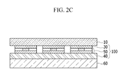
- FIGS. 2A to 2F illustrate process views showing stages of the method of manufacturing the display panel according to the exemplary embodiment.
- FIG. 3 illustrates a cross-sectional view showing a unit display panel cut into a cell unit, to which an upper passivation film is attached, according to the exemplary embodiment.
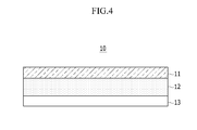
- FIG. 4 illustrates a cross-sectional view of the upper passivation film according to the exemplary embodiment.
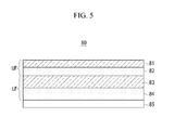
- FIG. 5 illustrates a cross-sectional view of the upper passivation film according to another exemplary embodiment.
- FIG. 6 illustrates a cross-sectional view showing formation of a hard coating layer on the upper passivation film according to yet another exemplary embodiment.
- FIG. 7 illustrates a cross-sectional view of the upper passivation film according to yet another exemplary embodiment.
- FIG. 8 illustrates a cross-sectional view of the upper passivation film according to still another exemplary embodiment.
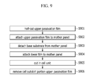
- FIG. 9 illustrates a flowchart showing a method of manufacturing the display panel according to another exemplary embodiment.
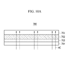
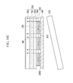
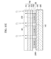
- FIGS. 10A to 10F illustrate process views showing each step of the method of manufacturing the display panel according to another exemplary embodiment.
- FIGS. 1 and 2A to 2F a method of manufacturing a display panel according to an exemplary embodiment will be described with reference to FIGS. 1 and 2A to 2F.
- FIG. 1 illustrates a flowchart showing a method of manufacturing a display panel according to an exemplary embodiment.
- reference characters S101 through S106 referring to stages illustrated in the flowchart, are in parentheses.
- FIGS. 2A to 2F are process views showing stages of the method of manufacturing the display panel according to the exemplary embodiment.
- a mother panel 100 including a display substrate 40, a display device layer 50 formed on the display substrate 40, and a thin film encapsulation layer 30 formed on the display device layer 50 is provided on a base substrate 20.
- the base substrate 20 attached to the display substrate 40 may provide sufficient thickness to enable convenient handling of the mother panel 100.
- the display substrate 40 may be a flexible polyimide (PI) substrate.
- PI polyimide
- the mother panel 100 may include a plurality of display device layers 50 and corresponding thin encapsulation layers 30 spaced apart from each other on the display substrate 40.
- the display device layer 50 may be an organic light emitting display device layer.
- the thin film encapsulation layer 30 may be formed as an organic and inorganic complex layer by alternately laminating one or more organic layers and one or more inorganic layers. The entire display device layer 50 may be covered by the thin film encapsulation layer 30 to be protected from the external air.
- the thin film encapsulation layer 30 is illustrated schematically.
- the display substrate 40 may be manufactured using a melt-extrusion method of performing biaxial stretching after melting to manufacture a substrate, or using a solvent caster method of mixing and dissolving additives and plastics to ensure fluidity and then passing the resulting structure through a slit die having a fixed thickness to volatilize a solvent, thus molding a plastic substrate.
- the upper passivation film 10 is attached to the thin film encapsulation layer 30 of the mother panel 100 (S101).
- the upper passivation film 10 may initially be made up of a carrier film 11, an adhesive layer 12, and a release film 13. After the release film 13 is removed, the adhesive layer 12 may be attached to the thin film encapsulation layer 30.
- the base substrate 20 is detached from the display substrate 40 of the mother panel 100 (S102).
- a lower film 60 is attached to the display substrate 40 of the mother panel 100 (S103).
- the lower film 60 is attached to the display substrate 40 to prevent or hinder a surface of the display substrate 40 from being damaged when a subsequent process is performed.
- the mother panel 100 to which the upper passivation film 10 and the lower film 60 are attached is cut to provide a unit display panel 200 (S104).
- the cell cutting may be performed using a method such as laser cutting or cutting by a physical unit (e.g., knife).
- a unit display panel 200 according to the exemplary embodiment shown in FIG. 3 is manufactured.
- the method of manufacturing the display panel according an embodiment, as shown in FIGS. 2E and 2F may further include removing the upper passivation film 10 from the thin film encapsulation layer 30 of the unit display panel 200 cut in the cell unit (S105) and attaching a functional layer 70 to the thin film encapsulation layer 30 (S106).
- FIG. 3 illustrates a cross-sectional view showing the unit display panel 200 cut into the form of a cell unit, to which the upper passivation film is attached, according to the exemplary embodiment.
- the unit display panel 200 includes the display substrate 40, the display device layer 50, and the thin film encapsulation layer 30.
- the upper passivation film 10 is attached to the thin film encapsulation layer 30, and the lower film 60 is attached to the display substrate 40.
- the unit display panel 200 may be a liquid crystal display panel including liquid crystal, or an organic light emitting panel including an organic light emitting portion.
- the display substrate 40 may be a transparent substrate, and/or a flexible substrate such as a polymer film.
- the display device layer 50 may be formed on the display substrate 40, and may include a device region, in which an active device such as a thin film transistor (TFT) is formed, and a light emitting region, in which an emission layer is formed.
- TFT thin film transistor
- the thin film encapsulation layer 30 is formed on the display device layer 50, and faces the display substrate 40. The thin film encapsulation layer 30 may prevent or hinder an inflow of oxygen and moisture from the outside to protect the display device layer 50.
- the thin film encapsulation layer 30 may be formed by alternately laminating one or more organic layers and one or more inorganic layers.
- the inorganic layer or the organic layer may be each provided in plural.
- the organic layer may be formed of a polymer, and may be, for example, a single layer or a laminated layer formed of any one of polyethylene terephthalate, polyimide, polycarbonate, epoxy, polyethylene, and polyacrylate.
- the organic layer may be formed of polyacrylate, and may include a material obtained by polymerizing a monomer composition including a diacrylate-based monomer and a triacrylate-based monomer.
- a monoacrylate-based monomer may be further included in the monomer composition.
- a suitable photoinitiator such as TPO may be further included in the monomer composition, for example.
- the inorganic layer may be a single layer or a laminated layer including metal oxide or metal nitride.
- the inorganic layer may include any one of SiN x , Al 2 O 3 , SiO 2 , and TiO 2 .
- the uppermost layer of the thin film encapsulation layer 30, which is exposed to the outside, may be formed of an inorganic layer in order to prevent or hinder permeation of moisture to an organic light emitting device.
- the thin film encapsulation layer 30 may include at least one sandwich structure in which at least one organic layer is inserted between at least two inorganic layers.
- the thin film encapsulation layer 30 may include at least one sandwich structure in which at least one inorganic layer is inserted between at least two organic layers.
- the thin film encapsulation layer 30 may include a first inorganic layer, a first organic layer, and a second inorganic layer sequentially disposed from an upper portion of the display device layer 50.
- the thin film encapsulation layer 30 may include the first inorganic layer, the first organic layer, the second inorganic layer, a second organic layer, and a third inorganic layer sequentially disposed from the upper portion of the display device layer 50.
- the thin film encapsulation layer 30 may include the first inorganic layer, the first organic layer, the second inorganic layer, the second organic layer, the third inorganic layer, a third organic layer, and a fourth inorganic layer sequentially disposed from the upper portion of the display device layer 50.
- a halogenated metal layer including LiF may be further included between the display device layer 50 and the first inorganic layer.
- the halogenated metal layer may prevent or hinder the display device layer 50 from being damaged when the first inorganic layer is formed by a sputtering method or a plasma deposition method.
- the first organic layer may have an area that is smaller than that of the second inorganic layer.
- the second organic layer may have an area that is smaller than that of the third inorganic layer.
- the first organic layer may be completely covered by the second inorganic layer.
- the second organic layer may be completely covered by the third inorganic layer.
- the upper passivation film 10 is attached to the thin film encapsulation layer 30.
- the upper passivation film 10 may protect the thin film encapsulation layer 30.
- the thin film encapsulation layer 30 may be a thin film having a small thickness, and may cover an organic light emitting material constituting the display device layer 50.
- damage such as stabbing or scratches may easily occur. For example, damage may be produced by an alien substance generated by external scratching or when an additional process, such as a cell cutting process, is performed. Such damage may result in noticeable defects such as dark spots on the display.
- the upper passivation film 10 may protect the surface of the thin film encapsulation layer 30 when the additional process is performed. Accordingly, limitations that may otherwise be imposed to protect the thin film encapsulation layer 30 may be removed or disregarded if the upper passivation film 10 is present when the additional process is performed.
- the upper passivation film may 10 be formed of a transparent material. Inspection of the unit display panel 200 may be performed when a transparent film is used as the upper passivation film 10. Further, process marks may be confirmed in equipment, and thus, limitations with respect to equipment/methods for performing of the additional process may be reduced.
- the lower film 60 may be attached to the display substrate 40, and prevents the surface of the display substrate 40 from being damaged when the process is performed.
- FIG. 4 illustrates a cross-sectional view of the upper passivation film 10 according to the exemplary embodiment.
- the upper passivation film 10 may initially include the carrier film 11, the adhesive layer 12, and the release film 13.
- the release film 13 may be a protection paper for preventing the adhesive layer 12 from coming into contact with contaminants and with the outside.
- the release film 13 is removed before the upper passivation film 10 is attached to the thin film encapsulation layer 30 to attach the adhesive layer 12 to the thin film encapsulation layer 30.
- the carrier film 11 may be formed of any one of polyethylene terephthalate (PET), polyethylene naphthalate (PEN), polyethylene sulfide (PES), and polyethylene (PE).
- PET polyethylene terephthalate
- PEN polyethylene naphthalate
- PS polyethylene sulfide
- PE polyethylene
- the carrier film 11 may have a thickness of about 25 to 300 micrometers ( ⁇ m).
- the adhesive layer 12 may be maintained to be attached to the thin film encapsulation layer 30 when a cell cutting process is performed and may be removed when a cell cutting process which will be described below is finished and another functional layer is attached. Accordingly, upper/lower limitations of adhesion strength are desirable.
- the adhesive layer may have adhesion strength of about 1 to 50 gf/inch when stainless steel (for example, steel use stainless, SUS) is an adherent.
- peeling of the upper passivation film 10/removal of the outskirt portion may be prevented or reduced when the cell cutting process is performed and/or damage (such as, for example, stripping of the surface layer) to the thin film encapsulation layer 30 may be reduced or prevented when the upper passivation film 10 is removed.
- the adhesive layer 12 may have adhesion strength of 3.7 to 8.4 gf/inch when polyethylene terephthalate (PET) is the adherent.
- PET polyethylene terephthalate
- the adhesive layer 12 may be a silicone, acrylic, or urethane-based low adhesive film.
- FIG. 5 illustrates a cross-sectional view of the upper passivation film 80 according to another exemplary embodiment.
- an upper passivation film 80 may be constituted by a first carrier film 81, a first adhesive layer 82 formed on a lower portion of the first carrier film 81, a second carrier film 83 formed on a lower portion of the first adhesive layer 82, a second adhesive layer 84 formed on a lower portion of the second carrier film 83, and a release film (liner) 85 attached to a lower portion of the second adhesive layer 84.
- the upper passivation film 80 may have a double structure including an upper film UF formed of the first carrier film 81 and the first adhesive layer 82 and a lower film LF formed of the second carrier film 83 and the second adhesive layer 84.
- the release film 85 may be a protection paper for preventing the second adhesive layer 84 from coming into contact with contaminants and with the outside. The release film 85 is removed before the upper passivation film 80 is attached to the thin film encapsulation layer 30 to attach the second adhesive layer 84 to the thin film encapsulation layer 30.
- the first carrier film 81 and the second carrier film 83 may be formed of any one ofpolyethylene terephthalate (PET), polyethylene naphthalate (PEN), polyethylene sulfide (PES), and polyethylene (PE).
- PET polyethylene terephthalate
- PEN polyethylene naphthalate
- PS polyethylene sulfide
- PE polyethylene
- the second carrier film 83 may have a thickness of about 25 to 300 micrometers ( ⁇ m).
- the second adhesive layer 84 may have adhesion strength of about 1 to 50 gf/inch when stainless steel (steel use stainless, SUS) is the adherent, and may have adhesion strength of about 3.7 to 8.4 gf/inch when polyethylene terephthalate (PET) is the adherent.
- a modified structure of the upper passivation film 80 is a double structure.
- Adhesion strength of the first adhesive layer 82 may be the same as or smaller than adhesion strength of the second adhesive layer 84.
- the first carrier film 81 and the second carrier film 83 may be attached due to attachment strength such as electrostatic force or surface tension without the first adhesive layer 82.
- the visual examination may be performed by removing the first carrier film 81.
- FIG. 6 illustrates a cross-sectional view showing formation of a hard coating layer on the upper passivation film according to yet another exemplary embodiment.
- the hard coating layer 94 may be formed on the upper portion of the upper passivation film.
- FIG. 6 shows formation of the hard coating layer 94 on the single upper passivation film constituted by a carrier film 91, an adhesive layer 92, and a release film 93.
- the structure 90 in which the hard coating layer 94 is further included in the upper portion of the upper passivation film may be applied to all structures of the aforementioned single or double upper passivation film.
- the hard coating layer 94 may be formed by applying an acryl-based urethane onto the surface of the carrier film 91 at the upper portion of the upper passivation film and then radiating the acryl-based urethane with ultraviolet rays (UV) to perform curing.
- UV ultraviolet rays
- the hard coating layer 94 may have a thickness of about 3 to 4 micrometers ( ⁇ m).
- the hard coating layer 94 may prevent or hinder scratches from occurring in the carrier film 91 of the upper passivation film in equipment processing and performing of distribution.
- the hard coating layer 94 may be formed of a transparent material, and vision alignment or panel visual examination may be performed while the hard coating layer 94 and the upper passivation film are attached.
- the method of manufacturing the display panel as shown in FIGS. 2E and 2F may further include removing the upper passivation film 10 from the thin film encapsulation layer 30 of the unit display panel 200 cut into the form of the cell unit (S105) and attaching a functional layer 70 to the thin film encapsulation layer 30 (S106).
- the functional layer 70 may be a polarizer, a touch screen panel, or a light efficiency or brightness increasing film.
- a selection range may be widened by removing the upper passivation film 10 and attaching the functional layer 70 to the thin film encapsulation layer 30 for the various purposes.
- a polarizer or a touch screen panel may be attached to the organic light emitting display panel.
- the present method allows for selectivity, for example, in attaching a touch screen panel instead of a polarizer.
- a light efficiency increasing film or a brightness increasing film may be attached in a cut state to the unit display panel 200 to increase the degree of freedom of the display panel structure.
- the polarizer and the touch screen panel are attached to an undivided mother substrate, it may be difficult to directly manufacture the polarizer and the touch screen panel as the upper film because there may be great damage and loss in yield and area.
- a temporary upper passivation film is used, according to embodiments, a large merit may be ensured in terms of the degree of freedom of the structure.
- FIG. 7 illustrates a cross-sectional view of the upper passivation film 700 according to yet another exemplary embodiment.
- the upper passivation film 700 itself may include a functional layer 702.
- the upper passivation film 700 may initially include a functional layer 702, a functional layer passivation film 701 formed on an upper portion of the functional layer 702, an adhesive layer 703 formed on a lower portion of the functional layer 702, and a release film 704 attached to a lower portion of the adhesive layer 703.
- the release film 704 may be removed to attach the adhesive layer to the thin film encapsulation layer 30.
- the adhesive layer 703 may have adhesion strength of about 0.2 to 2 kgf/inch when stainless steel (steel use stainless (SUS)) is an adherent.
- the adhesive layer 703 may be a silicone, acrylic, or urethane-based low adhesive film.
- the functional layer 702 may be a polarizer, a touch screen panel, or a light efficiency or brightness increasing film.
- FIG. 8 is a cross-sectional view of a upper passivation film 800 according to still another exemplary embodiment.
- the upper passivation film 800 may further include a dummy passivation film 805 in addition to the upper passivation film 700 shown in FIG. 7 .
- the upper passivation film 800 may initially be constituted by a functional layer 802, a functional layer passivation film 801 formed on the functional layer 802, a dummy passivation film 805 formed on an upper portion of the functional layer passivation film 801, an adhesive layer 803 formed on a lower portion of the functional layer 802, and a release film 804 attached to a lower portion of the adhesive layer 803.
- the release film 804 may be removed to attach the adhesive layer 803 to the thin film encapsulation layer 30.
- the adhesive layer 803 may have adhesion strength of about 0.2 to 2 kgf/inch when stainless steel (steel use stainless (SUS)) is the adherent.
- the adhesive layer 803 may be a silicone, acrylic, or urethane-based film.
- the functional layer 802 may be a polarizer, a touch screen panel, or a light efficiency or brightness increasing film.
- FIG. 9 illustrates a flowchart showing a method of manufacturing the display panel according to another exemplary embodiment
- FIGS. 10A to 10F illustrate process views showing stages of the method of manufacturing the display panel according to this exemplary embodiment.
- a mother panel 1000 including a thin film encapsulation layer 130 encapsulating a display substrate 140 on which a display device layer 150 is formed is provided on a base substrate 120.
- An outskirt portion of the display substrate 140 may be exposed and a pad portion may be formed at the outskirt portion of the display substrate 140. Accordingly, the pad portion may be opened to the outside after cell cutting.
- half cutting may be performed such that the functional layer 702, the adhesive layer 703, and the release film 704 remain on the cell outskirt portion 142 other than a surface of the upper passivation film 700, on which the display device layer 150 is formed (S901).
- a half cutting line HC may be cut to only a portion of a thickness of the functional layer passivation film 701 in view of a cross-section to remove the release film 704, the adhesive layer 703, the functional layer 702, and the functional layer passivation film 701 of the cell outskirt portion 142 together after cutting the mother panel 1000 into the unit display panel 2000.
- Cutting may be performed such that the release film 704 remains on the cell outskirt portion 142, Accordingly, two half cutting lines HC may be formed on respective sides of the unit display panel 2000 based on the cell outskirt portion 142.
- the release film of the surface on which the display device layer 150 is formed may be removed, and the half cut upper passivation film 700 may be attached to the thin film encapsulation layer 130 (S902).
- the adhesive layer 703 of the upper passivation film 700 may be attached to the thin film encapsulation layer 130 corresponding to the display device layer 150.
- the base substrate 120 which may provide sufficient thickness to enable convenient handling of the mother panel 1000, may be detached from the display substrate (S903).
- the lower film 160 may be attached to the display substrate after the base substrate 120 is detached (S904).
- the lower film 160 may be attached to the display substrate to prevent a surface of the display substrate from being damaged when an additional process is performed.
- the mother panel 1000 to which the upper passivation film 700 and the lower film 160 are attached is cut to provide a unit display panel 2000 (S905).
- the cell cutting may be performed using a method such as laser cutting or cutting by a physical unit (e.g., knife).
- the half cutting line HC including the surface on which the display device layer 150 is formed and the cell outskirt portion 142 is cut among the two half cutting lines HC formed on both sides based on the cell outskirt portion 142.
- the upper passivation film 700 at the cell outskirt portion 142 is removed (S906).
- the functional layer passivation film 701 formed on the upper portion of the functional layer 702, and the functional layer 702, the adhesive layer 703, and the release film 704 of the cell outskirt portion 142 are removed (S906).
- the functional layer 702, the adhesive layer 703, and the release film 704 may be cut in advance along another half cutting line HC among the two half cutting lines formed on both sides based on the cell outskirt portion 142. Accordingly, when the functional layer passivation film 701 is peeled off, the functional layer 702, the adhesive layer 703, and the release film 704 of the cell outskirt portion 142 may be easily removed.
- the removing of the upper passivation film of the cell outskirt portion may be performed such that end surfaces of the functional layer 702 corresponding to the surface on which the display device layer 150 is formed and the adhesive layer 703 coincide with an end surface of the display device layer 150.
- the upper passivation film 700 shown in FIGS. 9 and 10A to 10F may further include a dummy passivation film on the functional layer passivation film 701.
- the functional layer 702 may be a polarizer, a touch screen panel, or a light efficiency or brightness increasing film.
- Adhesion strength of the adhesive layer 703 may be changed by irradiating the adhesive layer with ultraviolet rays (UV).
- UV ultraviolet rays
- the adhesive layer 703 may be obtained using a material changing adhesion strength using ultraviolet rays (UV) to remove the step.
- a display device may typically include a thin film transistor, a display substrate including an emission layer, and an encapsulation substrate covering the display substrate.
- the display substrate is encapsulated using thin film glass in order to prevent moisture and oxygen from penetrating an organic material that is a light emitting body.
- a thin film encapsulation process is used.
- damages such as stab marks or scratches may easily occur due an alien substance generated by external scratching or when a process such as a cutting process is performed, thus causing defects such as dark spots on the display.
- Embodiments may improve productivity, a process ability, and a yield by providing a method in which an upper passivation film is attached onto a thin film encapsulation layer on a substrate in the original substrate state and then subsequent processes ae performed to manufacture a display panel.
- the method of manufacturing the display panel may be easy to handle the display panel in equipment and movement of automation distribution and it may be possible to protect the thin film encapsulation layer to prevent damages such as stabbing or scratches by an alien substance generated by external scratching or when a process is performed by attaching the upper passivation film to the thin film encapsulation layer and performing the process. Further, it may be possible to perform inspection of the display panel and confirm process marks in equipment by using a transparent material as the upper passivation film. Accordingly, limitations in equipment/performing of the process may be reduced or eliminated. Further, after the upper passivation film is removed, a functional layer such as a touch screen panel or a light efficiency or brightness increasing film may be attached. Thus, a degree of freedom of the display panel structure may be increased.
- the upper passivation film it is possible to reduce or remove a possibility of an occurrence of defects by constituting the upper passivation film to have the functional layer and maintaining the upper passivation film on the thin film encapsulation layer to affect a physical structure of the device according to removal of the upper passivation film.
Landscapes
- Physics & Mathematics (AREA)
- Engineering & Computer Science (AREA)
- Manufacturing & Machinery (AREA)
- Nonlinear Science (AREA)
- Mathematical Physics (AREA)
- Chemical & Material Sciences (AREA)
- Crystallography & Structural Chemistry (AREA)
- General Physics & Mathematics (AREA)
- Optics & Photonics (AREA)
- Microelectronics & Electronic Packaging (AREA)
- Devices For Indicating Variable Information By Combining Individual Elements (AREA)
- Electroluminescent Light Sources (AREA)
Description
- Example embodiments relate to a method of manufacturing a display panel.
- Display devices include liquid crystal displays (LCD), plasma display panels (PDP), organic light emitting diode (OLED) displays, field effect displays (FED), and electrophoretic display devices.
- Embodiments are directed to a method of manufacturing a display panel including forming a mother panel on a base substrate, attaching an upper passivation film to the mother panel, detaching the base substrate from the mother panel, attaching a lower film to the mother panel, and cutting the mother panel to which the upper passivation film and the lower film are attached to form the display panel, the display panel being in a form of a cell unit, wherein the display panel includes a display substrate, a display device layer, and a thin film encapsulation layer.
- The upper passivation film may initially include a carrier film, an adhesive layer formed on a lower portion of the carrier film, and a release film attached to a lower portion of the adhesive layer. The method may include removing the release film to attach the adhesive layer to the thin film encapsulation layer.
- The carrier film may be formed of any one of polyethylene terephthalate, polyethylene naphthalate, polyethylene sulfide, and polyethylene.
- The carrier film may have a thickness of about 25 to 300 µm.
- The adhesive layer may have adhesion strength of about 1 to 50 gf/inch when stainless steel (SUS) is an adherent.
- The adhesive layer may be a silicone, acrylic, or urethane-based film.
- The upper passivation film may initially includes a first carrier film, a first adhesive layer formed on a lower portion of the first carrier film lower, a second carrier film formed on a lower portion of the first adhesive layer, a second adhesive layer formed on a lower portion of the second carrier film, and the release film attached to a lower portion of the second adhesive layer. The method may further include removing the release film to attach the second adhesive layer to the thin film encapsulation layer.
- The first carrier film and the second carrier film may be formed of any one of polyethylene terephthalate, polyethylene naphthalate, polyethylene sulfide, and polyethylene.
- The second carrier film may have a thickness of about 25 to 300 µm.
- The second adhesive layer may have an adhesion strength of about 1 to 50 gf/inch when stainless steel (SUS) is an adherent.
- The first adhesive layer and the second adhesive layer may each individually be a silicone, acrylic, or urethane-based film.
- An adhesion strength of the first adhesive layer may be the same as or smaller than the adhesion strength of the second adhesive layer.
- The method may further include forming a hard coating layer on an upper portion of the upper passivation film.
- The hard coating layer may have a thickness of about 3 to 4 µm.
- The hard coating layer may be formed by applying an acryl-based urethane onto the upper portion of the upper passivation film and then performing ultraviolet (UV) curing.
- The display substrate may be a flexible substrate.
- The upper passivation film may be formed of a transparent material.
- The method may further include removing the upper passivation film from the thin film encapsulation layer of the display panel in the form of the cell unit, and attaching a functional layer to the thin film encapsulation layer.
- The functional layer may be a polarizer.
- The functional layer may be a touch screen panel.
- The functional layer may be a light efficiency or brightness increasing film.
- The upper passivation film may initially includes a functional layer, a functional layer passivation film formed on an upper portion of the functional layer, an adhesive layer formed on a lower portion of the functional layer, and a release film attached to the lower portion of the adhesive layer. The method may further include removing the release film to attach the adhesive layer to the thin film encapsulation layer.
- The adhesive layer may have an adhesion strength of about 0.2 to 2 kgfinch when stainless steel is an adherent.
- The method may further include, before attaching the upper passivation film to the mother panel, performing half-cutting such that the functional layer, the adhesive layer, and the release film remain on a cell outskirt portion other than a surface on which the display device layer is formed.
- The method may further include, after cutting the mother panel to form the display panel in the form of the cell unit, removing upper passivation film, the functional layer, the adhesive layer and the release film from the cell outskirt portion, and the adhesive layer from the cell outskirt portion.
- The removing of the cell outskirt portion upper passivation film may be performed such that end surfaces of the functional layer corresponding to the surface on which the display device layer is formed and the adhesive layer coincide with an end surface of the display device layer.
- The functional layer may be a polarizer.
- The functional layer may be a touch screen panel.
- The functional layer may be a light efficiency or brightness increasing film.
- The upper passivation film may further include a dummy passivation film on the functional layer passivation film.
- An adhesion strength of the adhesive layer may be changed by ultraviolet rays (UV).
- Features will become apparent to those of skill in the art by describing in detail example embodiments with reference to the attached drawings in which:
-
FIG. 1 illustrates a flowchart showing a method of manufacturing a display panel according to an exemplary embodiment. -
FIGS. 2A to 2F illustrate process views showing stages of the method of manufacturing the display panel according to the exemplary embodiment. -
FIG. 3 illustrates a cross-sectional view showing a unit display panel cut into a cell unit, to which an upper passivation film is attached, according to the exemplary embodiment. -
FIG. 4 illustrates a cross-sectional view of the upper passivation film according to the exemplary embodiment. -
FIG. 5 illustrates a cross-sectional view of the upper passivation film according to another exemplary embodiment. -
FIG. 6 illustrates a cross-sectional view showing formation of a hard coating layer on the upper passivation film according to yet another exemplary embodiment. -
FIG. 7 illustrates a cross-sectional view of the upper passivation film according to yet another exemplary embodiment. -
FIG. 8 illustrates a cross-sectional view of the upper passivation film according to still another exemplary embodiment. -
FIG. 9 illustrates a flowchart showing a method of manufacturing the display panel according to another exemplary embodiment. -
FIGS. 10A to 10F illustrate process views showing each step of the method of manufacturing the display panel according to another exemplary embodiment. - In the drawing figures, the dimensions of layers and regions may be exaggerated for clarity of illustration. It will also be understood that when a layer or element is referred to as being "on" another layer or substrate, it can be directly on the other layer or substrate, or intervening layers may also be present. In addition, it will also be understood that when a layer is referred to as being "between" two layers, it can be the only layer between the two layers, or one or more intervening layers may also be present. Like reference numerals refer to like elements throughout.
- Hereinafter, a method of manufacturing a display panel according to an exemplary embodiment will be described with reference to
FIGS. 1 and2A to 2F. -
FIG. 1 illustrates a flowchart showing a method of manufacturing a display panel according to an exemplary embodiment. In the following description, reference characters S101 through S106, referring to stages illustrated in the flowchart, are in parentheses.FIGS. 2A to 2F are process views showing stages of the method of manufacturing the display panel according to the exemplary embodiment. - Referring to
FIGS. 1 and2A to 2F , first, amother panel 100 including adisplay substrate 40, adisplay device layer 50 formed on thedisplay substrate 40, and a thinfilm encapsulation layer 30 formed on thedisplay device layer 50 is provided on abase substrate 20. Thebase substrate 20 attached to thedisplay substrate 40 may provide sufficient thickness to enable convenient handling of themother panel 100. Thedisplay substrate 40 may be a flexible polyimide (PI) substrate. It is to be understood that themother panel 100 may include a plurality of display device layers 50 and corresponding thin encapsulation layers 30 spaced apart from each other on thedisplay substrate 40. - The
display device layer 50 may be an organic light emitting display device layer. The thinfilm encapsulation layer 30 may be formed as an organic and inorganic complex layer by alternately laminating one or more organic layers and one or more inorganic layers. The entiredisplay device layer 50 may be covered by the thinfilm encapsulation layer 30 to be protected from the external air. InFIGS. 1 through 3 , the thinfilm encapsulation layer 30 is illustrated schematically. - The
display substrate 40 may be manufactured using a melt-extrusion method of performing biaxial stretching after melting to manufacture a substrate, or using a solvent caster method of mixing and dissolving additives and plastics to ensure fluidity and then passing the resulting structure through a slit die having a fixed thickness to volatilize a solvent, thus molding a plastic substrate. - As shown in
FIG. 2A , theupper passivation film 10 according to the exemplary embodiment is attached to the thinfilm encapsulation layer 30 of the mother panel 100 (S101). As shown inFIG. 4 , theupper passivation film 10 may initially be made up of acarrier film 11, anadhesive layer 12, and arelease film 13. After therelease film 13 is removed, theadhesive layer 12 may be attached to the thinfilm encapsulation layer 30. - As shown in
FIG. 2B , thebase substrate 20 is detached from thedisplay substrate 40 of the mother panel 100 (S102). - As shown in
FIG. 2C , after thebase substrate 20 is detached, alower film 60 is attached to thedisplay substrate 40 of the mother panel 100 (S103). Thelower film 60 is attached to thedisplay substrate 40 to prevent or hinder a surface of thedisplay substrate 40 from being damaged when a subsequent process is performed. - As shown in
FIG. 2D , themother panel 100 to which theupper passivation film 10 and thelower film 60 are attached is cut to provide a unit display panel 200 (S104). The cell cutting may be performed using a method such as laser cutting or cutting by a physical unit (e.g., knife). Thereby, aunit display panel 200 according to the exemplary embodiment shown inFIG. 3 is manufactured. - The method of manufacturing the display panel according an embodiment, as shown in
FIGS. 2E and2F , may further include removing theupper passivation film 10 from the thinfilm encapsulation layer 30 of theunit display panel 200 cut in the cell unit (S105) and attaching afunctional layer 70 to the thin film encapsulation layer 30 (S106). -
FIG. 3 illustrates a cross-sectional view showing theunit display panel 200 cut into the form of a cell unit, to which the upper passivation film is attached, according to the exemplary embodiment. Referring toFIG. 3 , theunit display panel 200 includes thedisplay substrate 40, thedisplay device layer 50, and the thinfilm encapsulation layer 30. Theupper passivation film 10 is attached to the thinfilm encapsulation layer 30, and thelower film 60 is attached to thedisplay substrate 40. - The
unit display panel 200 may be a liquid crystal display panel including liquid crystal, or an organic light emitting panel including an organic light emitting portion. Thedisplay substrate 40 may be a transparent substrate, and/or a flexible substrate such as a polymer film. Thedisplay device layer 50 may be formed on thedisplay substrate 40, and may include a device region, in which an active device such as a thin film transistor (TFT) is formed, and a light emitting region, in which an emission layer is formed. The thinfilm encapsulation layer 30 is formed on thedisplay device layer 50, and faces thedisplay substrate 40. The thinfilm encapsulation layer 30 may prevent or hinder an inflow of oxygen and moisture from the outside to protect thedisplay device layer 50. - The thin
film encapsulation layer 30 may be formed by alternately laminating one or more organic layers and one or more inorganic layers. - The inorganic layer or the organic layer may be each provided in plural.
- The organic layer may be formed of a polymer, and may be, for example, a single layer or a laminated layer formed of any one of polyethylene terephthalate, polyimide, polycarbonate, epoxy, polyethylene, and polyacrylate. For example, the organic layer may be formed of polyacrylate, and may include a material obtained by polymerizing a monomer composition including a diacrylate-based monomer and a triacrylate-based monomer. A monoacrylate-based monomer may be further included in the monomer composition. Further, a suitable photoinitiator such as TPO may be further included in the monomer composition, for example.
- The inorganic layer may be a single layer or a laminated layer including metal oxide or metal nitride. For example, the inorganic layer may include any one of SiNx, Al2O3, SiO2, and TiO2.
- The uppermost layer of the thin
film encapsulation layer 30, which is exposed to the outside, may be formed of an inorganic layer in order to prevent or hinder permeation of moisture to an organic light emitting device. - The thin
film encapsulation layer 30 may include at least one sandwich structure in which at least one organic layer is inserted between at least two inorganic layers. In an implementation, the thinfilm encapsulation layer 30 may include at least one sandwich structure in which at least one inorganic layer is inserted between at least two organic layers. - The thin
film encapsulation layer 30 may include a first inorganic layer, a first organic layer, and a second inorganic layer sequentially disposed from an upper portion of thedisplay device layer 50. In an implementation, the thinfilm encapsulation layer 30 may include the first inorganic layer, the first organic layer, the second inorganic layer, a second organic layer, and a third inorganic layer sequentially disposed from the upper portion of thedisplay device layer 50. In an implementation, the thinfilm encapsulation layer 30 may include the first inorganic layer, the first organic layer, the second inorganic layer, the second organic layer, the third inorganic layer, a third organic layer, and a fourth inorganic layer sequentially disposed from the upper portion of thedisplay device layer 50. - A halogenated metal layer including LiF may be further included between the
display device layer 50 and the first inorganic layer. The halogenated metal layer may prevent or hinder thedisplay device layer 50 from being damaged when the first inorganic layer is formed by a sputtering method or a plasma deposition method. - The first organic layer may have an area that is smaller than that of the second inorganic layer. The second organic layer may have an area that is smaller than that of the third inorganic layer. The first organic layer may be completely covered by the second inorganic layer. The second organic layer may be completely covered by the third inorganic layer.
- The
upper passivation film 10 is attached to the thinfilm encapsulation layer 30. Theupper passivation film 10 may protect the thinfilm encapsulation layer 30. The thinfilm encapsulation layer 30 may be a thin film having a small thickness, and may cover an organic light emitting material constituting thedisplay device layer 50. With regard to the thinfilm encapsulation layer 30, damage such as stabbing or scratches may easily occur. For example, damage may be produced by an alien substance generated by external scratching or when an additional process, such as a cell cutting process, is performed. Such damage may result in noticeable defects such as dark spots on the display. When theupper passivation film 10 is used in order to prevent or reduce the likelihood of damage to the thinfilm encapsulation layer 30, theupper passivation film 10 may protect the surface of the thinfilm encapsulation layer 30 when the additional process is performed. Accordingly, limitations that may otherwise be imposed to protect the thinfilm encapsulation layer 30 may be removed or disregarded if theupper passivation film 10 is present when the additional process is performed. - The upper passivation film may 10 be formed of a transparent material. Inspection of the
unit display panel 200 may be performed when a transparent film is used as theupper passivation film 10. Further, process marks may be confirmed in equipment, and thus, limitations with respect to equipment/methods for performing of the additional process may be reduced. - The
lower film 60 may be attached to thedisplay substrate 40, and prevents the surface of thedisplay substrate 40 from being damaged when the process is performed. -
FIG. 4 illustrates a cross-sectional view of theupper passivation film 10 according to the exemplary embodiment. Referring toFIG. 4 , theupper passivation film 10 may initially include thecarrier film 11, theadhesive layer 12, and therelease film 13. - The
release film 13 may be a protection paper for preventing theadhesive layer 12 from coming into contact with contaminants and with the outside. Therelease film 13 is removed before theupper passivation film 10 is attached to the thinfilm encapsulation layer 30 to attach theadhesive layer 12 to the thinfilm encapsulation layer 30. - The
carrier film 11 may be formed of any one of polyethylene terephthalate (PET), polyethylene naphthalate (PEN), polyethylene sulfide (PES), and polyethylene (PE). - The
carrier film 11 may have a thickness of about 25 to 300 micrometers (µm). - The
adhesive layer 12 may be maintained to be attached to the thinfilm encapsulation layer 30 when a cell cutting process is performed and may be removed when a cell cutting process which will be described below is finished and another functional layer is attached. Accordingly, upper/lower limitations of adhesion strength are desirable. The adhesive layer may have adhesion strength of about 1 to 50 gf/inch when stainless steel (for example, steel use stainless, SUS) is an adherent. When theadhesive layer 12 has adhesion strength within this range, peeling of theupper passivation film 10/removal of the outskirt portion may be prevented or reduced when the cell cutting process is performed and/or damage (such as, for example, stripping of the surface layer) to the thinfilm encapsulation layer 30 may be reduced or prevented when theupper passivation film 10 is removed. - The
adhesive layer 12 may have adhesion strength of 3.7 to 8.4 gf/inch when polyethylene terephthalate (PET) is the adherent. - The
adhesive layer 12 may be a silicone, acrylic, or urethane-based low adhesive film. -
FIG. 5 illustrates a cross-sectional view of theupper passivation film 80 according to another exemplary embodiment. Referring toFIG. 5 , anupper passivation film 80 may be constituted by afirst carrier film 81, a firstadhesive layer 82 formed on a lower portion of thefirst carrier film 81, asecond carrier film 83 formed on a lower portion of the firstadhesive layer 82, a secondadhesive layer 84 formed on a lower portion of thesecond carrier film 83, and a release film (liner) 85 attached to a lower portion of the secondadhesive layer 84. - The
upper passivation film 80 may have a double structure including an upper film UF formed of thefirst carrier film 81 and the firstadhesive layer 82 and a lower film LF formed of thesecond carrier film 83 and the secondadhesive layer 84. Therelease film 85 may be a protection paper for preventing the secondadhesive layer 84 from coming into contact with contaminants and with the outside. Therelease film 85 is removed before theupper passivation film 80 is attached to the thinfilm encapsulation layer 30 to attach the secondadhesive layer 84 to the thinfilm encapsulation layer 30. - The
first carrier film 81 and thesecond carrier film 83 may be formed of any one ofpolyethylene terephthalate (PET), polyethylene naphthalate (PEN), polyethylene sulfide (PES), and polyethylene (PE). - The
second carrier film 83 may have a thickness of about 25 to 300 micrometers (µm). - The second
adhesive layer 84 may have adhesion strength of about 1 to 50 gf/inch when stainless steel (steel use stainless, SUS) is the adherent, and may have adhesion strength of about 3.7 to 8.4 gf/inch when polyethylene terephthalate (PET) is the adherent. As described above, a modified structure of theupper passivation film 80 is a double structure. - Adhesion strength of the first
adhesive layer 82 may be the same as or smaller than adhesion strength of the secondadhesive layer 84. In another implementation, thefirst carrier film 81 and thesecond carrier film 83 may be attached due to attachment strength such as electrostatic force or surface tension without the firstadhesive layer 82. - When the aforementioned
upper passivation film 10 having the monolayer structure is used, scratches may occur due to equipment stage vacuum holes in equipment and performing of distribution, causing defects in visual alignment or hindering panel visual examination by equipment in a post-process. In the structure of theupper passivation film 80 of the present exemplary embodiment, the visual examination may be performed by removing thefirst carrier film 81. -
FIG. 6 illustrates a cross-sectional view showing formation of a hard coating layer on the upper passivation film according to yet another exemplary embodiment. Referring toFIG. 6 , thehard coating layer 94 may be formed on the upper portion of the upper passivation film.FIG. 6 shows formation of thehard coating layer 94 on the single upper passivation film constituted by acarrier film 91, anadhesive layer 92, and a release film 93. However, it is to be understood that thestructure 90 in which thehard coating layer 94 is further included in the upper portion of the upper passivation film may be applied to all structures of the aforementioned single or double upper passivation film. - The
hard coating layer 94 may be formed by applying an acryl-based urethane onto the surface of thecarrier film 91 at the upper portion of the upper passivation film and then radiating the acryl-based urethane with ultraviolet rays (UV) to perform curing. - The
hard coating layer 94 may have a thickness of about 3 to 4 micrometers (µm). - The
hard coating layer 94 may prevent or hinder scratches from occurring in thecarrier film 91 of the upper passivation film in equipment processing and performing of distribution. Like the upper passivation film, thehard coating layer 94 may be formed of a transparent material, and vision alignment or panel visual examination may be performed while thehard coating layer 94 and the upper passivation film are attached. - The method of manufacturing the display panel as shown in
FIGS. 2E and2F , following the process stages shown inFIGS. 2A to 2D , may further include removing theupper passivation film 10 from the thinfilm encapsulation layer 30 of theunit display panel 200 cut into the form of the cell unit (S105) and attaching afunctional layer 70 to the thin film encapsulation layer 30 (S106). - The
functional layer 70 may be a polarizer, a touch screen panel, or a light efficiency or brightness increasing film. - In the
unit display panel 200 cut into the form of a cell unit, a selection range may be widened by removing theupper passivation film 10 and attaching thefunctional layer 70 to the thinfilm encapsulation layer 30 for the various purposes. For example, a polarizer or a touch screen panel may be attached to the organic light emitting display panel. Compared to a process in which a polarizer is attached at an early stage such that the polarizer is always attached onto the display panel, the present method allows for selectivity, for example, in attaching a touch screen panel instead of a polarizer. - Further, in addition to the polarizer or the touch screen panel, a light efficiency increasing film or a brightness increasing film may be attached in a cut state to the
unit display panel 200 to increase the degree of freedom of the display panel structure. When the polarizer and the touch screen panel are attached to an undivided mother substrate, it may be difficult to directly manufacture the polarizer and the touch screen panel as the upper film because there may be great damage and loss in yield and area. On the other hand, when a temporary upper passivation film is used, according to embodiments, a large merit may be ensured in terms of the degree of freedom of the structure. -
FIG. 7 illustrates a cross-sectional view of theupper passivation film 700 according to yet another exemplary embodiment. Referring toFIG. 7 , theupper passivation film 700 itself may include afunctional layer 702. Theupper passivation film 700 may initially include afunctional layer 702, a functionallayer passivation film 701 formed on an upper portion of thefunctional layer 702, anadhesive layer 703 formed on a lower portion of thefunctional layer 702, and arelease film 704 attached to a lower portion of theadhesive layer 703. Therelease film 704 may be removed to attach the adhesive layer to the thinfilm encapsulation layer 30. - The
adhesive layer 703 may have adhesion strength of about 0.2 to 2 kgf/inch when stainless steel (steel use stainless (SUS)) is an adherent. Theadhesive layer 703 may be a silicone, acrylic, or urethane-based low adhesive film. - The
functional layer 702 may be a polarizer, a touch screen panel, or a light efficiency or brightness increasing film. -
FIG. 8 is a cross-sectional view of aupper passivation film 800 according to still another exemplary embodiment. Referring toFIG. 8 , theupper passivation film 800 may further include adummy passivation film 805 in addition to theupper passivation film 700 shown inFIG. 7 . Theupper passivation film 800 may initially be constituted by afunctional layer 802, a functionallayer passivation film 801 formed on thefunctional layer 802, adummy passivation film 805 formed on an upper portion of the functionallayer passivation film 801, anadhesive layer 803 formed on a lower portion of thefunctional layer 802, and arelease film 804 attached to a lower portion of theadhesive layer 803. Therelease film 804 may be removed to attach theadhesive layer 803 to the thinfilm encapsulation layer 30. - The
adhesive layer 803 may have adhesion strength of about 0.2 to 2 kgf/inch when stainless steel (steel use stainless (SUS)) is the adherent. Theadhesive layer 803 may be a silicone, acrylic, or urethane-based film. Thefunctional layer 802 may be a polarizer, a touch screen panel, or a light efficiency or brightness increasing film. -
FIG. 9 illustrates a flowchart showing a method of manufacturing the display panel according to another exemplary embodiment, andFIGS. 10A to 10F illustrate process views showing stages of the method of manufacturing the display panel according to this exemplary embodiment. - Referring to
FIGS. 9 and10A to 10F, first, amother panel 1000 including a thinfilm encapsulation layer 130 encapsulating adisplay substrate 140 on which adisplay device layer 150 is formed is provided on abase substrate 120. An outskirt portion of thedisplay substrate 140 may be exposed and a pad portion may be formed at the outskirt portion of thedisplay substrate 140. Accordingly, the pad portion may be opened to the outside after cell cutting. - As shown in
FIGS. 10A and10B , half cutting may be performed such that thefunctional layer 702, theadhesive layer 703, and therelease film 704 remain on thecell outskirt portion 142 other than a surface of theupper passivation film 700, on which thedisplay device layer 150 is formed (S901). In this case, a half cutting line HC may be cut to only a portion of a thickness of the functionallayer passivation film 701 in view of a cross-section to remove therelease film 704, theadhesive layer 703, thefunctional layer 702, and the functionallayer passivation film 701 of thecell outskirt portion 142 together after cutting themother panel 1000 into theunit display panel 2000. Cutting may be performed such that therelease film 704 remains on thecell outskirt portion 142, Accordingly, two half cutting lines HC may be formed on respective sides of theunit display panel 2000 based on thecell outskirt portion 142. - As shown in
FIG. 10B , the release film of the surface on which thedisplay device layer 150 is formed may be removed, and the half cutupper passivation film 700 may be attached to the thin film encapsulation layer 130 (S902). Theadhesive layer 703 of theupper passivation film 700 may be attached to the thinfilm encapsulation layer 130 corresponding to thedisplay device layer 150. - As shown in
FIG. 10C , thebase substrate 120, which may provide sufficient thickness to enable convenient handling of themother panel 1000, may be detached from the display substrate (S903). - As shown in
FIG. 10D , thelower film 160 may be attached to the display substrate after thebase substrate 120 is detached (S904). Thelower film 160 may be attached to the display substrate to prevent a surface of the display substrate from being damaged when an additional process is performed. - As shown in
FIG. 10E , themother panel 1000 to which theupper passivation film 700 and thelower film 160 are attached is cut to provide a unit display panel 2000 (S905). The cell cutting may be performed using a method such as laser cutting or cutting by a physical unit (e.g., knife). The half cutting line HC including the surface on which thedisplay device layer 150 is formed and thecell outskirt portion 142 is cut among the two half cutting lines HC formed on both sides based on thecell outskirt portion 142. - Thereafter, as shown in
FIG. 10F , in theunit display panel 2000 cut into the form of a cell unit, theupper passivation film 700 at thecell outskirt portion 142 is removed (S906). The functionallayer passivation film 701 formed on the upper portion of thefunctional layer 702, and thefunctional layer 702, theadhesive layer 703, and therelease film 704 of thecell outskirt portion 142 are removed (S906). As described above, thefunctional layer 702, theadhesive layer 703, and therelease film 704 may be cut in advance along another half cutting line HC among the two half cutting lines formed on both sides based on thecell outskirt portion 142. Accordingly, when the functionallayer passivation film 701 is peeled off, thefunctional layer 702, theadhesive layer 703, and therelease film 704 of thecell outskirt portion 142 may be easily removed. - The removing of the upper passivation film of the cell outskirt portion (S906) may be performed such that end surfaces of the
functional layer 702 corresponding to the surface on which thedisplay device layer 150 is formed and theadhesive layer 703 coincide with an end surface of thedisplay device layer 150. - The
upper passivation film 700 shown inFIGS. 9 and10A to 10F may further include a dummy passivation film on the functionallayer passivation film 701. Thefunctional layer 702 may be a polarizer, a touch screen panel, or a light efficiency or brightness increasing film. Adhesion strength of theadhesive layer 703 may be changed by irradiating the adhesive layer with ultraviolet rays (UV). When therelease film 704 remains on thecell outskirt portion 142, bubbles may be generated due to a step,. In order to prevent the generation of bubbles, theadhesive layer 703 may be obtained using a material changing adhesion strength using ultraviolet rays (UV) to remove the step. - By way of summation and review, a display device may typically include a thin film transistor, a display substrate including an emission layer, and an encapsulation substrate covering the display substrate. In the case of an organic light emitting diode display, the display substrate is encapsulated using thin film glass in order to prevent moisture and oxygen from penetrating an organic material that is a light emitting body. In a flexible OLED display, a thin film encapsulation process is used. However, in a thin film encapsulation layer, damages such as stab marks or scratches may easily occur due an alien substance generated by external scratching or when a process such as a cutting process is performed, thus causing defects such as dark spots on the display.
- Embodiments may improve productivity, a process ability, and a yield by providing a method in which an upper passivation film is attached onto a thin film encapsulation layer on a substrate in the original substrate state and then subsequent processes ae performed to manufacture a display panel.
- As described above, by the method of manufacturing the display panel according to the exemplary embodiment, it may be easy to handle the display panel in equipment and movement of automation distribution and it may be possible to protect the thin film encapsulation layer to prevent damages such as stabbing or scratches by an alien substance generated by external scratching or when a process is performed by attaching the upper passivation film to the thin film encapsulation layer and performing the process. Further, it may be possible to perform inspection of the display panel and confirm process marks in equipment by using a transparent material as the upper passivation film. Accordingly, limitations in equipment/performing of the process may be reduced or eliminated. Further, after the upper passivation film is removed, a functional layer such as a touch screen panel or a light efficiency or brightness increasing film may be attached. Thus, a degree of freedom of the display panel structure may be increased.
- Further, it is possible to reduce or remove a possibility of an occurrence of defects by constituting the upper passivation film to have the functional layer and maintaining the upper passivation film on the thin film encapsulation layer to affect a physical structure of the device according to removal of the upper passivation film.
- It is clear for a person skilled in the art that the disclosed embodiments can also be combined where possible.
Claims (15)
- A method of manufacturing a display panel, the method comprising:forming a mother panel (100) on a base substrate (20);attaching an upper passivation film (10) to the mother panel (100) (S101);detaching the base substrate (20) from the mother panel (100) (S102);attaching a lower film (60) to the mother panel (100) (S103); andcutting the mother panel (100) to which the upper passivation film (10) and the lower film (60) are attached to form the display panel (200), the display panel (200) being in a form of a cell unit (S104),wherein the display panel includes a display substrate (40), a display device layer (50), and a thin film encapsulation layer (30).
- The method of manufacturing a display panel as claimed in claim 1, wherein:the upper passivation film (10) initially includes a carrier film (11), an adhesive layer (12) formed on a lower portion of the carrier film (11), and a release film (13) attached to a lower portion of the adhesive layer (12), andthe method includes removing the release film (13) to attach the adhesive layer (12) to the thin film encapsulation layer (30).
- The method of manufacturing a display panel as claimed in claim 1 or 2, wherein the adhesive layer (12) has an adhesion strength of about 1 to 50 gf/inch when stainless steel (SUS) is an adherent.
- The method of manufacturing a display panel as claimed in claim 1, wherein:the upper passivation film (80) initially includes a first carrier film (81), a first adhesive layer (82) formed on a lower portion of the first carrier film (81), a second carrier film (83) formed on a lower portion of the first adhesive layer (82), a second adhesive layer (84) formed on a lower portion of the second carrier film (83), and a release film (85) attached to a lower portion of the second adhesive layer(84), andthe method further comprises removing the release film (85) to attach the second adhesive layer (84) to the thin film encapsulation layer (30).
- The method of manufacturing a display panel as claimed in claim 4, wherein an adhesion strength of the first adhesive layer (82) is the same as or smaller than the adhesion strength of the second adhesive layer (84).
- The method of manufacturing a display panel as claimed in claim 1 to 5, further comprising forming a hard coating layer (94) on an upper portion of the upper passivation film (10, 80).
- The method of manufacturing a display panel as claimed in claim 6, wherein the upper passivation film (10, 80) and/or the hard coating layer (94) is formed of a transparent material.
- The method of manufacturing a display panel as claimed in one of claims 1 to 7, further comprising:removing the upper passivation film (10) from the thin film encapsulation layer (30) of the display panel (200) in the form of the cell unit (S105); andattaching a functional layer (70) to the thin film encapsulation layer (30) (S106).
- The method of manufacturing a display panel as claimed in claim 8, wherein the functional layer (70) is a polarizer, a touch screen panel, or a light efficiency or brightness increasing film.
- The method of manufacturing a display panel as claimed in claim 1, wherein the upper passivation film (700) initially includes a functional layer (70), a functional layer passivation film (701) formed on an upper portion of the functional layer (70), an adhesive layer (703) formed on a lower portion of the functional layer (70), and a release film (704) attached to the lower portion of the adhesive layer (703), and the method includes removing the release film (704) to attach the adhesive layer (703) to the thin film encapsulation layer (30), and/or.
the adhesive layer (703) has an adhesion strength of about 0.2 to 2 kgf/inch when stainless steel is an adherent. - The method of manufacturing a display panel as claimed in claim 10, further comprising, before attaching the upper passivation film (700) to the mother panel (1000), performing half-cutting (S901) such that when the upper passivation film (700) is attached to the mother panel (1000), the functional layer (702), the adhesive layer (703), and the release film (704) remain on a cell outskirt portion (142) other than a surface on which the display device layer (150) is formed.
- The method of manufacturing a display panel as claimed in claim 11, further comprising:after cutting the mother panel (1000) to form the display panel (2000) in the form of the cell unit, removing the functional layer passivation film (701), the functional layer (702), the adhesive layer (703), and the release film (704) from the cell outskirt portion (142).
- The method of manufacturing a display panel as claimed in claim 12, wherein:the removing the functional layer passivation film (701), the functional layer (702), the adhesive layer (703), and the release film (704) from the cell outskirt portion (142) is performed such that end surfaces of the functional layer (702) corresponding to the surface on which the display device layer (150) is formed and the adhesive layer (703) coincide with an end surface of the display device layer (150).
- The method of manufacturing a display panel as claimed in claim 10, wherein the upper passivation film (800) further includes a dummy passivation film (805) on the functional layer passivation film (801).
- The method of manufacturing a display panel as claimed in one of claims 10 to 14 , wherein an adhesion strength of the adhesive layer (703) is changed by ultraviolet rays (UV).
Applications Claiming Priority (2)
| Application Number | Priority Date | Filing Date | Title |
|---|---|---|---|
| KR20120076845 | 2012-07-13 | ||
| KR1020130057292A KR102060541B1 (en) | 2012-07-13 | 2013-05-21 | Method of manufacturing display panel |
Publications (2)
| Publication Number | Publication Date |
|---|---|
| EP2685516A1 true EP2685516A1 (en) | 2014-01-15 |
| EP2685516B1 EP2685516B1 (en) | 2019-10-16 |
Family
ID=48793922
Family Applications (1)
| Application Number | Title | Priority Date | Filing Date |
|---|---|---|---|
| EP13176241.1A Active EP2685516B1 (en) | 2012-07-13 | 2013-07-12 | Method of manufacturing a display panel |
Country Status (3)
| Country | Link |
|---|---|
| US (1) | US9673014B2 (en) |
| EP (1) | EP2685516B1 (en) |
| CN (1) | CN103544885B (en) |
Families Citing this family (21)
| Publication number | Priority date | Publication date | Assignee | Title |
|---|---|---|---|---|
| KR102173048B1 (en) * | 2013-12-18 | 2020-11-03 | 삼성디스플레이 주식회사 | Display apparatus having distance maintenance parts |
| CN104167513A (en) * | 2014-07-22 | 2014-11-26 | 京东方科技集团股份有限公司 | Manufacturing method of flexible display panel and flexible display device |
| JP6335099B2 (en) * | 2014-11-04 | 2018-05-30 | 東芝メモリ株式会社 | Semiconductor device and manufacturing method of semiconductor device |
| TW201624668A (en) * | 2014-12-16 | 2016-07-01 | 友達光電股份有限公司 | Flexible panel |
| KR102288354B1 (en) * | 2015-08-10 | 2021-08-11 | 삼성디스플레이 주식회사 | Method for manufacturing flexible display apparatus |
| KR102548461B1 (en) * | 2016-06-10 | 2023-06-28 | 삼성디스플레이 주식회사 | Display device and method for manufacturing the same |
| KR102671371B1 (en) * | 2016-10-07 | 2024-06-04 | 삼성디스플레이 주식회사 | Flexible display apparatus and manufacturing method thereof |
| CN107403882B (en) * | 2017-08-08 | 2019-09-17 | 京东方科技集团股份有限公司 | A kind of preparation method of flexible display |
| KR102083315B1 (en) | 2017-09-11 | 2020-03-03 | 삼성디스플레이 주식회사 | Organic light-emitting display device and method of manufacturing the same |
| US11355733B2 (en) | 2017-10-23 | 2022-06-07 | Lg Chem, Ltd. | Optical film having antistatic layers, optical film manufacturing method, and organic light-emitting electronic device manufacturing method |
| KR102193857B1 (en) | 2017-10-23 | 2020-12-22 | 주식회사 엘지화학 | Optical film, method of manufacturing optical film and method of manufacturing organic light emitting electronic device |
| CN108188590B (en) * | 2017-12-28 | 2020-02-18 | 武汉华星光电半导体显示技术有限公司 | Cutting method of flexible media |
| CN108389514A (en) * | 2018-02-08 | 2018-08-10 | 武汉天马微电子有限公司 | A kind of flexible display screen and display device |
| CN110570754B (en) * | 2018-06-05 | 2022-01-04 | 上海和辉光电股份有限公司 | Manufacturing method of flexible display panel and flexible display panel |
| KR102602157B1 (en) | 2018-06-29 | 2023-11-14 | 삼성디스플레이 주식회사 | Organic light-emitting display device and method of manufacturing the same |
| CN109696991A (en) * | 2018-12-06 | 2019-04-30 | 信利光电股份有限公司 | A kind of production method of OLED touch-control display module |
| CN109860418A (en) * | 2019-01-29 | 2019-06-07 | 昆山国显光电有限公司 | A kind of display panel and preparation method thereof |
| CN110444682B (en) * | 2019-07-25 | 2022-02-11 | 苏州清越光电科技股份有限公司 | Display panel, preparation process thereof and display device comprising same |
| WO2021102921A1 (en) * | 2019-11-29 | 2021-06-03 | 京东方科技集团股份有限公司 | Display panel motherboard, cutting method and manufacturing method therefor, display panel, and display device |
| KR102907812B1 (en) | 2020-07-23 | 2026-01-06 | 삼성디스플레이 주식회사 | Panel substrate and manufacturing method for display device including the panel substrate |
| KR102920611B1 (en) * | 2021-03-17 | 2026-02-02 | 삼성디스플레이 주식회사 | Display device and method of manufacturing the same |
Citations (3)
| Publication number | Priority date | Publication date | Assignee | Title |
|---|---|---|---|---|
| US20110156062A1 (en) * | 2009-12-24 | 2011-06-30 | Samsung Mobile Display Co., Ltd. | Organic light-emitting display device and method of manufacturing the same |
| US20120009702A1 (en) * | 2010-07-07 | 2012-01-12 | Samsung Mobile Display Co, Ltd. | Method for manufacturing organic light emitting diode display |
| US20120098026A1 (en) * | 2010-10-25 | 2012-04-26 | Samsung Mobile Display Co., Ltd. | Organic Light Emitting Diode Display and Method for Manufacturing Organic Light Emitting Diode Display |
Family Cites Families (18)
| Publication number | Priority date | Publication date | Assignee | Title |
|---|---|---|---|---|
| US6204906B1 (en) * | 1999-03-22 | 2001-03-20 | Lawrence E. Tannas, Jr. | Methods of customizing the physical size and shape of commercial off-the-shelf (COTS) electronic displays |
| KR20040027940A (en) * | 2001-08-20 | 2004-04-01 | 노바-플라즈마 인크. | Coatings with low permeation of gases and vapors |
| JP4104489B2 (en) | 2002-05-17 | 2008-06-18 | 東芝松下ディスプレイテクノロジー株式会社 | Display device and manufacturing method thereof |
| KR20040002796A (en) | 2002-06-28 | 2004-01-07 | 후지 샤신 필름 가부시기가이샤 | Method and apparatus for bonding polarizing plate |
| US8147640B2 (en) * | 2005-05-13 | 2012-04-03 | Lg Display Co., Ltd. | Fabricating method of flexible display |
| CN100428010C (en) | 2005-05-13 | 2008-10-22 | 乐金显示有限公司 | Manufacturing method of flexible display |
| KR101168731B1 (en) | 2005-09-06 | 2012-07-26 | 삼성전자주식회사 | Substrate for liquid crystal display |
| JP2008004917A (en) | 2006-05-24 | 2008-01-10 | Fujitsu Ltd | Pattern forming method and semiconductor device manufacturing method |
| KR20080023853A (en) | 2006-09-12 | 2008-03-17 | 삼성전자주식회사 | Device for manufacturing flexible display device and method for manufacturing same |
| JP5208591B2 (en) * | 2007-06-28 | 2013-06-12 | 株式会社半導体エネルギー研究所 | Light emitting device and lighting device |
| US8182633B2 (en) * | 2008-04-29 | 2012-05-22 | Samsung Electronics Co., Ltd. | Method of fabricating a flexible display device |
| KR100989125B1 (en) * | 2008-07-16 | 2010-10-20 | 삼성모바일디스플레이주식회사 | A mother substrate cutting device and an organic light emitting display device cut thereby |
| JP5525446B2 (en) * | 2008-09-09 | 2014-06-18 | 株式会社きもと | Laminated plate and display device |
| JP2011003522A (en) | 2008-10-16 | 2011-01-06 | Semiconductor Energy Lab Co Ltd | Flexible light-emitting device, electronic equipment, and method of manufacturing flexible light-emitting device |
| KR101155907B1 (en) | 2009-06-04 | 2012-06-20 | 삼성모바일디스플레이주식회사 | Organic light emitting diode display and method for manufacturing the same |
| JP4503693B1 (en) | 2009-10-13 | 2010-07-14 | 日東電工株式会社 | Continuous roll of cut-lined optical film laminate in the form of a continuous web, its manufacturing method and manufacturing apparatus |
| KR101142198B1 (en) | 2009-12-21 | 2012-05-07 | 도레이첨단소재 주식회사 | Adhesive Protective Film for Flexible Print Circuit Board |
| KR101084180B1 (en) | 2009-12-28 | 2011-11-17 | 삼성모바일디스플레이주식회사 | Polarizing plate and organic light emitting display device having the same |
-
2013
- 2013-06-28 US US13/930,836 patent/US9673014B2/en active Active
- 2013-07-12 CN CN201310293586.0A patent/CN103544885B/en active Active
- 2013-07-12 EP EP13176241.1A patent/EP2685516B1/en active Active
Patent Citations (3)
| Publication number | Priority date | Publication date | Assignee | Title |
|---|---|---|---|---|
| US20110156062A1 (en) * | 2009-12-24 | 2011-06-30 | Samsung Mobile Display Co., Ltd. | Organic light-emitting display device and method of manufacturing the same |
| US20120009702A1 (en) * | 2010-07-07 | 2012-01-12 | Samsung Mobile Display Co, Ltd. | Method for manufacturing organic light emitting diode display |
| US20120098026A1 (en) * | 2010-10-25 | 2012-04-26 | Samsung Mobile Display Co., Ltd. | Organic Light Emitting Diode Display and Method for Manufacturing Organic Light Emitting Diode Display |
Also Published As
| Publication number | Publication date |
|---|---|
| CN103544885B (en) | 2018-09-11 |
| CN103544885A (en) | 2014-01-29 |
| US20140017967A1 (en) | 2014-01-16 |
| US9673014B2 (en) | 2017-06-06 |
| EP2685516B1 (en) | 2019-10-16 |
Similar Documents
| Publication | Publication Date | Title |
|---|---|---|
| EP2685516B1 (en) | Method of manufacturing a display panel | |
| KR102060541B1 (en) | Method of manufacturing display panel | |
| US8557637B2 (en) | Method for fabricating the flexible electronic device | |
| KR102741535B1 (en) | Method of manufacturing organic light emitting display device | |
| EP2894689B1 (en) | Method for manufacturing flexible display device | |
| KR101057151B1 (en) | Manufacturing Method of Flexible Glass Substrate and Flexible Glass Substrate | |
| US9431630B2 (en) | Package structure for flexible organic light emitting diode device, method for packaging the same and flexible display device | |
| EP2743753B1 (en) | Method for manufacturing a flexible display device | |
| TWI428243B (en) | Method for debonding a flexible device | |
| US20160141552A1 (en) | Flexible display and method for fabricating the same | |
| CN113314582B (en) | A flexible display substrate, manufacturing method thereof and display panel | |
| KR20110133881A (en) | Flexible substrate for display device and manufacturing method thereof | |
| CN103681357A (en) | Flexible display device, flexible display device manufacturing method and display unit | |
| KR102793699B1 (en) | Method of manufacturing organic light emitting display device | |
| JP6283062B2 (en) | Display device manufacturing method | |
| CN103996698A (en) | Manufacturing method of flexible panel | |
| US20210050559A1 (en) | Method for manufacturing display device | |
| JP2012226013A (en) | Methods of manufacturing electronic device and display apparatus | |
| KR101734224B1 (en) | Method for Manufacturing Flat Display Panel Device | |
| US20080048347A1 (en) | Display device and manufacturing method thereof | |
| JP2018026260A (en) | Display device manufacturing method | |
| CN110571355A (en) | Method for attaching barrier film on display panel, barrier film and display panel | |
| JP2018040930A (en) | Method for manufacturing liquid crystal display panel | |
| JP2008071616A (en) | Organic EL element panel and manufacturing method thereof | |
| JP2018073773A (en) | Method for manufacturing organic el device composite |
Legal Events
| Date | Code | Title | Description |
|---|---|---|---|
| PUAI | Public reference made under article 153(3) epc to a published international application that has entered the european phase |
Free format text: ORIGINAL CODE: 0009012 |
|
| AK | Designated contracting states |
Kind code of ref document: A1 Designated state(s): AL AT BE BG CH CY CZ DE DK EE ES FI FR GB GR HR HU IE IS IT LI LT LU LV MC MK MT NL NO PL PT RO RS SE SI SK SM TR |
|
| AX | Request for extension of the european patent |
Extension state: BA ME |
|
| 17P | Request for examination filed |
Effective date: 20140715 |
|
| RBV | Designated contracting states (corrected) |
Designated state(s): AL AT BE BG CH CY CZ DE DK EE ES FI FR GB GR HR HU IE IS IT LI LT LU LV MC MK MT NL NO PL PT RO RS SE SI SK SM TR |
|
| 17Q | First examination report despatched |
Effective date: 20150420 |
|
| RAP1 | Party data changed (applicant data changed or rights of an application transferred) |
Owner name: SAMSUNG DISPLAY CO., LTD. |
|
| STAA | Information on the status of an ep patent application or granted ep patent |
Free format text: STATUS: EXAMINATION IS IN PROGRESS |
|
| GRAP | Despatch of communication of intention to grant a patent |
Free format text: ORIGINAL CODE: EPIDOSNIGR1 |
|
| STAA | Information on the status of an ep patent application or granted ep patent |
Free format text: STATUS: GRANT OF PATENT IS INTENDED |
|
| INTG | Intention to grant announced |
Effective date: 20190509 |
|
| RIN1 | Information on inventor provided before grant (corrected) |
Inventor name: MUN, HYO-YOUNG Inventor name: CHO, HYUN-JUN Inventor name: KIM, YOUNG-GU Inventor name: KIM, YOUNG-JI |
|
| GRAS | Grant fee paid |
Free format text: ORIGINAL CODE: EPIDOSNIGR3 |
|
| GRAA | (expected) grant |
Free format text: ORIGINAL CODE: 0009210 |
|
| STAA | Information on the status of an ep patent application or granted ep patent |
Free format text: STATUS: THE PATENT HAS BEEN GRANTED |
|
| AK | Designated contracting states |
Kind code of ref document: B1 Designated state(s): AL AT BE BG CH CY CZ DE DK EE ES FI FR GB GR HR HU IE IS IT LI LT LU LV MC MK MT NL NO PL PT RO RS SE SI SK SM TR |
|
| REG | Reference to a national code |
Ref country code: GB Ref legal event code: FG4D |
|
| REG | Reference to a national code |
Ref country code: CH Ref legal event code: EP |
|
| REG | Reference to a national code |
Ref country code: DE Ref legal event code: R096 Ref document number: 602013061723 Country of ref document: DE |
|
| REG | Reference to a national code |
Ref country code: IE Ref legal event code: FG4D |
|
| REG | Reference to a national code |
Ref country code: AT Ref legal event code: REF Ref document number: 1192157 Country of ref document: AT Kind code of ref document: T Effective date: 20191115 |
|
| REG | Reference to a national code |
Ref country code: NL Ref legal event code: MP Effective date: 20191016 |
|
| REG | Reference to a national code |
Ref country code: LT Ref legal event code: MG4D |
|
| REG | Reference to a national code |
Ref country code: AT Ref legal event code: MK05 Ref document number: 1192157 Country of ref document: AT Kind code of ref document: T Effective date: 20191016 |
|
| PG25 | Lapsed in a contracting state [announced via postgrant information from national office to epo] |
Ref country code: ES Free format text: LAPSE BECAUSE OF FAILURE TO SUBMIT A TRANSLATION OF THE DESCRIPTION OR TO PAY THE FEE WITHIN THE PRESCRIBED TIME-LIMIT Effective date: 20191016 Ref country code: SE Free format text: LAPSE BECAUSE OF FAILURE TO SUBMIT A TRANSLATION OF THE DESCRIPTION OR TO PAY THE FEE WITHIN THE PRESCRIBED TIME-LIMIT Effective date: 20191016 Ref country code: LV Free format text: LAPSE BECAUSE OF FAILURE TO SUBMIT A TRANSLATION OF THE DESCRIPTION OR TO PAY THE FEE WITHIN THE PRESCRIBED TIME-LIMIT Effective date: 20191016 Ref country code: AT Free format text: LAPSE BECAUSE OF FAILURE TO SUBMIT A TRANSLATION OF THE DESCRIPTION OR TO PAY THE FEE WITHIN THE PRESCRIBED TIME-LIMIT Effective date: 20191016 Ref country code: PT Free format text: LAPSE BECAUSE OF FAILURE TO SUBMIT A TRANSLATION OF THE DESCRIPTION OR TO PAY THE FEE WITHIN THE PRESCRIBED TIME-LIMIT Effective date: 20200217 Ref country code: BG Free format text: LAPSE BECAUSE OF FAILURE TO SUBMIT A TRANSLATION OF THE DESCRIPTION OR TO PAY THE FEE WITHIN THE PRESCRIBED TIME-LIMIT Effective date: 20200116 Ref country code: GR Free format text: LAPSE BECAUSE OF FAILURE TO SUBMIT A TRANSLATION OF THE DESCRIPTION OR TO PAY THE FEE WITHIN THE PRESCRIBED TIME-LIMIT Effective date: 20200117 Ref country code: FI Free format text: LAPSE BECAUSE OF FAILURE TO SUBMIT A TRANSLATION OF THE DESCRIPTION OR TO PAY THE FEE WITHIN THE PRESCRIBED TIME-LIMIT Effective date: 20191016 Ref country code: NO Free format text: LAPSE BECAUSE OF FAILURE TO SUBMIT A TRANSLATION OF THE DESCRIPTION OR TO PAY THE FEE WITHIN THE PRESCRIBED TIME-LIMIT Effective date: 20200116 Ref country code: NL Free format text: LAPSE BECAUSE OF FAILURE TO SUBMIT A TRANSLATION OF THE DESCRIPTION OR TO PAY THE FEE WITHIN THE PRESCRIBED TIME-LIMIT Effective date: 20191016 Ref country code: LT Free format text: LAPSE BECAUSE OF FAILURE TO SUBMIT A TRANSLATION OF THE DESCRIPTION OR TO PAY THE FEE WITHIN THE PRESCRIBED TIME-LIMIT Effective date: 20191016 Ref country code: PL Free format text: LAPSE BECAUSE OF FAILURE TO SUBMIT A TRANSLATION OF THE DESCRIPTION OR TO PAY THE FEE WITHIN THE PRESCRIBED TIME-LIMIT Effective date: 20191016 |
|
| PG25 | Lapsed in a contracting state [announced via postgrant information from national office to epo] |
Ref country code: RS Free format text: LAPSE BECAUSE OF FAILURE TO SUBMIT A TRANSLATION OF THE DESCRIPTION OR TO PAY THE FEE WITHIN THE PRESCRIBED TIME-LIMIT Effective date: 20191016 Ref country code: HR Free format text: LAPSE BECAUSE OF FAILURE TO SUBMIT A TRANSLATION OF THE DESCRIPTION OR TO PAY THE FEE WITHIN THE PRESCRIBED TIME-LIMIT Effective date: 20191016 Ref country code: IS Free format text: LAPSE BECAUSE OF FAILURE TO SUBMIT A TRANSLATION OF THE DESCRIPTION OR TO PAY THE FEE WITHIN THE PRESCRIBED TIME-LIMIT Effective date: 20200224 |
|
| PG25 | Lapsed in a contracting state [announced via postgrant information from national office to epo] |
Ref country code: AL Free format text: LAPSE BECAUSE OF FAILURE TO SUBMIT A TRANSLATION OF THE DESCRIPTION OR TO PAY THE FEE WITHIN THE PRESCRIBED TIME-LIMIT Effective date: 20191016 |
|
| REG | Reference to a national code |
Ref country code: DE Ref legal event code: R097 Ref document number: 602013061723 Country of ref document: DE |
|
| PG2D | Information on lapse in contracting state deleted |
Ref country code: IS |
|
| PG25 | Lapsed in a contracting state [announced via postgrant information from national office to epo] |
Ref country code: EE Free format text: LAPSE BECAUSE OF FAILURE TO SUBMIT A TRANSLATION OF THE DESCRIPTION OR TO PAY THE FEE WITHIN THE PRESCRIBED TIME-LIMIT Effective date: 20191016 Ref country code: RO Free format text: LAPSE BECAUSE OF FAILURE TO SUBMIT A TRANSLATION OF THE DESCRIPTION OR TO PAY THE FEE WITHIN THE PRESCRIBED TIME-LIMIT Effective date: 20191016 Ref country code: CZ Free format text: LAPSE BECAUSE OF FAILURE TO SUBMIT A TRANSLATION OF THE DESCRIPTION OR TO PAY THE FEE WITHIN THE PRESCRIBED TIME-LIMIT Effective date: 20191016 Ref country code: DK Free format text: LAPSE BECAUSE OF FAILURE TO SUBMIT A TRANSLATION OF THE DESCRIPTION OR TO PAY THE FEE WITHIN THE PRESCRIBED TIME-LIMIT Effective date: 20191016 Ref country code: IS Free format text: LAPSE BECAUSE OF FAILURE TO SUBMIT A TRANSLATION OF THE DESCRIPTION OR TO PAY THE FEE WITHIN THE PRESCRIBED TIME-LIMIT Effective date: 20200216 |
|
| PLBE | No opposition filed within time limit |
Free format text: ORIGINAL CODE: 0009261 |
|
| STAA | Information on the status of an ep patent application or granted ep patent |
Free format text: STATUS: NO OPPOSITION FILED WITHIN TIME LIMIT |
|
| PG25 | Lapsed in a contracting state [announced via postgrant information from national office to epo] |
Ref country code: SM Free format text: LAPSE BECAUSE OF FAILURE TO SUBMIT A TRANSLATION OF THE DESCRIPTION OR TO PAY THE FEE WITHIN THE PRESCRIBED TIME-LIMIT Effective date: 20191016 Ref country code: IT Free format text: LAPSE BECAUSE OF FAILURE TO SUBMIT A TRANSLATION OF THE DESCRIPTION OR TO PAY THE FEE WITHIN THE PRESCRIBED TIME-LIMIT Effective date: 20191016 Ref country code: SK Free format text: LAPSE BECAUSE OF FAILURE TO SUBMIT A TRANSLATION OF THE DESCRIPTION OR TO PAY THE FEE WITHIN THE PRESCRIBED TIME-LIMIT Effective date: 20191016 |
|
| 26N | No opposition filed |
Effective date: 20200717 |
|
| PG25 | Lapsed in a contracting state [announced via postgrant information from national office to epo] |
Ref country code: SI Free format text: LAPSE BECAUSE OF FAILURE TO SUBMIT A TRANSLATION OF THE DESCRIPTION OR TO PAY THE FEE WITHIN THE PRESCRIBED TIME-LIMIT Effective date: 20191016 |
|
| PG25 | Lapsed in a contracting state [announced via postgrant information from national office to epo] |
Ref country code: MC Free format text: LAPSE BECAUSE OF FAILURE TO SUBMIT A TRANSLATION OF THE DESCRIPTION OR TO PAY THE FEE WITHIN THE PRESCRIBED TIME-LIMIT Effective date: 20191016 |
|
| REG | Reference to a national code |
Ref country code: CH Ref legal event code: PL |
|
| REG | Reference to a national code |
Ref country code: BE Ref legal event code: MM Effective date: 20200731 |
|
| PG25 | Lapsed in a contracting state [announced via postgrant information from national office to epo] |
Ref country code: LU Free format text: LAPSE BECAUSE OF NON-PAYMENT OF DUE FEES Effective date: 20200712 Ref country code: LI Free format text: LAPSE BECAUSE OF NON-PAYMENT OF DUE FEES Effective date: 20200731 Ref country code: CH Free format text: LAPSE BECAUSE OF NON-PAYMENT OF DUE FEES Effective date: 20200731 |
|
| PG25 | Lapsed in a contracting state [announced via postgrant information from national office to epo] |
Ref country code: BE Free format text: LAPSE BECAUSE OF NON-PAYMENT OF DUE FEES Effective date: 20200731 |
|
| PG25 | Lapsed in a contracting state [announced via postgrant information from national office to epo] |
Ref country code: IE Free format text: LAPSE BECAUSE OF NON-PAYMENT OF DUE FEES Effective date: 20200712 |
|
| PG25 | Lapsed in a contracting state [announced via postgrant information from national office to epo] |
Ref country code: TR Free format text: LAPSE BECAUSE OF FAILURE TO SUBMIT A TRANSLATION OF THE DESCRIPTION OR TO PAY THE FEE WITHIN THE PRESCRIBED TIME-LIMIT Effective date: 20191016 Ref country code: MT Free format text: LAPSE BECAUSE OF FAILURE TO SUBMIT A TRANSLATION OF THE DESCRIPTION OR TO PAY THE FEE WITHIN THE PRESCRIBED TIME-LIMIT Effective date: 20191016 Ref country code: CY Free format text: LAPSE BECAUSE OF FAILURE TO SUBMIT A TRANSLATION OF THE DESCRIPTION OR TO PAY THE FEE WITHIN THE PRESCRIBED TIME-LIMIT Effective date: 20191016 |
|
| PG25 | Lapsed in a contracting state [announced via postgrant information from national office to epo] |
Ref country code: MK Free format text: LAPSE BECAUSE OF FAILURE TO SUBMIT A TRANSLATION OF THE DESCRIPTION OR TO PAY THE FEE WITHIN THE PRESCRIBED TIME-LIMIT Effective date: 20191016 |
|
| REG | Reference to a national code |
Ref country code: DE Ref legal event code: R079 Ref document number: 602013061723 Country of ref document: DE Free format text: PREVIOUS MAIN CLASS: H01L0051560000 Ipc: H10K0050000000 |
|
| P01 | Opt-out of the competence of the unified patent court (upc) registered |
Effective date: 20230515 |
|
| PGFP | Annual fee paid to national office [announced via postgrant information from national office to epo] |
Ref country code: GB Payment date: 20250624 Year of fee payment: 13 |
|
| PGFP | Annual fee paid to national office [announced via postgrant information from national office to epo] |
Ref country code: FR Payment date: 20250624 Year of fee payment: 13 |
|
| PGFP | Annual fee paid to national office [announced via postgrant information from national office to epo] |
Ref country code: DE Payment date: 20250624 Year of fee payment: 13 |