EP2685498A2 - Dual anti-fuse - Google Patents
Dual anti-fuse Download PDFInfo
- Publication number
- EP2685498A2 EP2685498A2 EP13003395.4A EP13003395A EP2685498A2 EP 2685498 A2 EP2685498 A2 EP 2685498A2 EP 13003395 A EP13003395 A EP 13003395A EP 2685498 A2 EP2685498 A2 EP 2685498A2
- Authority
- EP
- European Patent Office
- Prior art keywords
- fuse
- channel
- programmable gate
- drain
- source
- Prior art date
- Legal status (The legal status is an assumption and is not a legal conclusion. Google has not performed a legal analysis and makes no representation as to the accuracy of the status listed.)
- Granted
Links
Images



Classifications
-
- H—ELECTRICITY
- H10—SEMICONDUCTOR DEVICES; ELECTRIC SOLID-STATE DEVICES NOT OTHERWISE PROVIDED FOR
- H10D—INORGANIC ELECTRIC SEMICONDUCTOR DEVICES
- H10D84/00—Integrated devices formed in or on semiconductor substrates that comprise only semiconducting layers, e.g. on Si wafers or on GaAs-on-Si wafers
- H10D84/201—Integrated devices formed in or on semiconductor substrates that comprise only semiconducting layers, e.g. on Si wafers or on GaAs-on-Si wafers characterised by the integration of only components covered by H10D1/00 or H10D8/00, e.g. RLC circuits
- H10D84/204—Integrated devices formed in or on semiconductor substrates that comprise only semiconducting layers, e.g. on Si wafers or on GaAs-on-Si wafers characterised by the integration of only components covered by H10D1/00 or H10D8/00, e.g. RLC circuits of combinations of diodes or capacitors or resistors
- H10D84/206—Integrated devices formed in or on semiconductor substrates that comprise only semiconducting layers, e.g. on Si wafers or on GaAs-on-Si wafers characterised by the integration of only components covered by H10D1/00 or H10D8/00, e.g. RLC circuits of combinations of diodes or capacitors or resistors of combinations of capacitors and resistors
-
- H—ELECTRICITY
- H10—SEMICONDUCTOR DEVICES; ELECTRIC SOLID-STATE DEVICES NOT OTHERWISE PROVIDED FOR
- H10B—ELECTRONIC MEMORY DEVICES
- H10B20/00—Read-only memory [ROM] devices
- H10B20/20—Programmable ROM [PROM] devices comprising field-effect components
- H10B20/25—One-time programmable ROM [OTPROM] devices, e.g. using electrically-fusible links
-
- H—ELECTRICITY
- H10—SEMICONDUCTOR DEVICES; ELECTRIC SOLID-STATE DEVICES NOT OTHERWISE PROVIDED FOR
- H10D—INORGANIC ELECTRIC SEMICONDUCTOR DEVICES
- H10D64/00—Electrodes of devices having potential barriers
- H10D64/20—Electrodes characterised by their shapes, relative sizes or dispositions
- H10D64/27—Electrodes not carrying the current to be rectified, amplified, oscillated or switched, e.g. gates
- H10D64/311—Gate electrodes for field-effect devices
- H10D64/411—Gate electrodes for field-effect devices for FETs
-
- H—ELECTRICITY
- H10—SEMICONDUCTOR DEVICES; ELECTRIC SOLID-STATE DEVICES NOT OTHERWISE PROVIDED FOR
- H10D—INORGANIC ELECTRIC SEMICONDUCTOR DEVICES
- H10D64/00—Electrodes of devices having potential barriers
- H10D64/60—Electrodes characterised by their materials
- H10D64/66—Electrodes having a conductor capacitively coupled to a semiconductor by an insulator, e.g. MIS electrodes
- H10D64/671—Electrodes having a conductor capacitively coupled to a semiconductor by an insulator, e.g. MIS electrodes the conductor having lateral variation in doping or structure
-
- H—ELECTRICITY
- H10—SEMICONDUCTOR DEVICES; ELECTRIC SOLID-STATE DEVICES NOT OTHERWISE PROVIDED FOR
- H10W—GENERIC PACKAGES, INTERCONNECTIONS, CONNECTORS OR OTHER CONSTRUCTIONAL DETAILS OF DEVICES COVERED BY CLASS H10
- H10W20/00—Interconnections in chips, wafers or substrates
- H10W20/40—Interconnections external to wafers or substrates, e.g. back-end-of-line [BEOL] metallisations or vias connecting to gate electrodes
- H10W20/49—Adaptable interconnections, e.g. fuses or antifuses
- H10W20/491—Antifuses, i.e. interconnections changeable from non-conductive to conductive
-
- H—ELECTRICITY
- H10—SEMICONDUCTOR DEVICES; ELECTRIC SOLID-STATE DEVICES NOT OTHERWISE PROVIDED FOR
- H10W—GENERIC PACKAGES, INTERCONNECTIONS, CONNECTORS OR OTHER CONSTRUCTIONAL DETAILS OF DEVICES COVERED BY CLASS H10
- H10W20/00—Interconnections in chips, wafers or substrates
- H10W20/40—Interconnections external to wafers or substrates, e.g. back-end-of-line [BEOL] metallisations or vias connecting to gate electrodes
- H10W20/49—Adaptable interconnections, e.g. fuses or antifuses
- H10W20/493—Fuses, i.e. interconnections changeable from conductive to non-conductive
Definitions
- An anti-fuse can be configured in a planar arrangement with a source, a drain, and a channel situated in a semiconductor substrate.
- a programmable gate is situated over the channel and includes a gate electrode situated over a gate dielectric.
- the gate dielectric initially provides a high-resistance current path between the gate electrode and the channel of the anti-fuse.
- the anti-fuse can be programmed by applying a programming voltage across the gate electrode and the channel so as cause breakdown of the gate dielectric. Once programmed, the current path changes from high-resistance to low-resistance to facilitate current flow through the current path.
- the present disclosure is directed to a dual anti-fuse, substantially as shown in and/or described in connection with at least one of the figures, and as set forth more completely in the claims.
- a dual anti-fuse structure comprises:
- said first programmable gate is on a first sidewall of said common semiconductor fin.
- said second programmable gate is on a second sidewall of said common semiconductor fin.
- said first programmable gate comprises a first gate dielectric and a first electrode.
- said first programmable gate comprises a second gate dielectric and a second electrode.
- said first anti-fuse comprises a first source and a first drain situated in said common semiconductor fin.
- said second anti-fuse comprises a second source and a second drain situated in said common semiconductor fin.
- said first channel is situated between said first programmable gate and said second programmable gate.
- said second channel is situated between said first programmable gate and said second programmable gate.
- said first channel and said second channel are situated in a common channel region.
- a dual anti-fuse structure comprises:
- said first source and said second source are situated in a common source region.
- said first drain and said second drain are situated in a common drain region.
- said first channel and said second channel are situated between said first source and said first drain.
- said first channel and said second channel are situated between said second source and said second drain.
- said first source and said second source are coupled to ground.
- said first drain and said second drain are coupled to ground.
- a dual anti-fuse structure comprises:
- said first electrode and said second electrode each comprise metal.
- said gate dielectric and said second gate dielectric each comprise high-k dielectric material.
- Figure 1 illustrates a schematic diagram of a circuit 100 including a dual anti-fuse structure 150.
- the dual anti-fuse structure 150 includes an anti-fuse 102a and an anti-fuse 102b.
- the anti-fuse 102a includes a source 104a, a drain 106a, a programmable gate 108a, and a channel 110a. Initially, the programmable gate 108a and the channel 110a form a high-resistance path for current flow.
- the source 104a and the drain 106a can be coupled to the high-resistance path through the channel 110a, as shown in Figure 1 .
- the anti-fuse 102a can be programmed by applying a programming voltage across the programmable gate 108a and the channel 110a so as cause breakdown of a gate dielectric in the programmable gate 108a. Once programmed, the high-resistance path changes from to a low-resistance path to facilitate current flow.
- the anti-fuse 102b includes a source 104b, a drain 106b, a programmable gate 108b, and a channel 110b.
- the programmable gate 108b and the channel 110b form a high-resistance path for current flow.
- the source 104b and the drain 106b can be coupled to the high-resistance path through the channel 110b, as shown in Figure 1 .
- the anti-fuse 102b can be programmed by applying a programming voltage across the programmable gate 108b and the channel 110b so as cause breakdown of a gate dielectric in the programmable gate 108b. Once programmed, the high-resistance path changes from to a low-resistance path to facilitate current flow.
- the source 104a of the anti-fuse 102a is coupled to the source 104b of the anti-fuse 102b. Furthermore, in the dual anti-fuse structure 150, the drain 106a of the anti-fuse 102a is coupled to the drain 106b of the anti-fuse 102b. However, in some implementations, the source 104a is not coupled to the source 104b and/or the drain 106a is not coupled to the drain 106b in the dual anti-fuse structure 150.
- the dual anti-fuse structure 150 can have many different configurations and can be utilized in many different circuits.
- the circuit 100 illustrates ones such circuit utilizing the dual-anti-fuse structure 150.
- the programmable gate 108a is coupled between a program transistor 114a and a read transistor 116a.
- the programmable gate 108b is coupled between a program transistor 114b and a read transistor 116b.
- the source 104a and the source 104b are coupled to a ground G 1 .
- the drain 106a and the drain 106b are coupled to a ground G 2 , which can be the same as the ground G 1 .
- the anti-fuse 102a can be programmed by, for example, applying a programming voltage V PP1 across the programmable gate 108a and the channel 110a through the program transistor 114a, which can be controlled by a gate 120a.
- the programming voltage V PP1 is sufficient to program the anti-fuse 102a by blowing the anti-fuse 102a.
- the anti-fuse 102a can be read from by, for example, applying a read voltage V DD1 to the programmable gate 108a through the read transistor 116a, which can be controlled by a gate 122a.
- the read voltage V DD1 can then be utilized to sense whether or not the anti-fuse 102a has been programmed based on the resistivity of the programmable gate 108a.
- the anti-fuse 102b can be programmed by, for example, applying a programming voltage V PP2 across the programmable gate 108b and the channel 110b through the program transistor 114b, which can be controlled by a gate 120b.
- the programming voltage V PP2 is sufficient to program the anti-fuse 102b by blowing the anti-fuse 102b.
- the anti-fuse 102b can be read from by, for example, applying a read voltage V DD2 to the programmable gate 108b through the read transistor 116b, which can be controlled by a gate 122b.
- the read voltage V DD2 can then be utilized to sense whether or not the anti-fuse 102b has been programmed based on the resistivity of the programmable gate 108b.
- the dual-anti fuse structure 150 includes the anti-fuse 102a and the anti-fuse 102b, which can optionally be independently operated as described above.
- the anti-fuse 102a described above includes the source 104a and the drain 106a for connection to the anti-fuse 102a.
- the source 104a and/or the drain 106a are not included in the dual anti-fuse structure 150 or are not utilized for connection to the anti-fuse 102a.
- the anti-fuse 102a can include the source 104a without the drain 106a or can include the drain 106a without the source 104a.
- the anti-fuse 102b described above includes the source 104b and the drain 106b for connection to the anti-fuse 102b.
- the source 104b and/or the drain 106b are not included in the dual anti-fuse structure 150 or are not utilized for connection to the anti-fuse 102b.
- the anti-fuse 102b can include the source 104b without the drain 106b or can include the drain 106b without the source 104b.
- utilizing the sources 104a and 104b and the drains 106a and 106b can offer various advantages including lowering the resistivity of the anti-fuses 102a and 102b after programming.
- Figure 2 shows a process flow diagram illustrating a process 200 for fabricating a dual anti-fuse structure, such as the dual anti-fuse structure 150 in Figure 1 .
- the dual anti-fuse structure 150 as well as other dual anti-fuse structures in accordance with the present disclosure, can be fabricated utilizing processes other than the process 200.
- the process 200 is described with respect to Figures 3A , 3B , and 3C .
- the implementation illustrated by the process 200 can be performed on a processed wafer, which prior to the process 200 may include a substrate having a source region, a drain region, and a channel region in a common semiconductor fin, a gate dielectric layer, and a field dielectric layer.
- the process 200 includes forming a conductive gate layer (e.g., 328) over a common semiconductor fin (e.g., 330) (270 in Figure 2 ).
- a conductive gate layer e.g., 328
- a common semiconductor fin e.g., 330
- Figure 3A illustrates a cross-sectional view of a potion of a wafer 370 during processing.
- the wafer 370 includes a substrate 332, a field dielectric layer 334, a common semiconductor fin 330, a gate dielectric layer 340, and a conductive gate layer 328.
- the substrate 332 includes semiconductor material, such as single-crystal semiconductor material.
- the substrate 332 is a silicon substrate and more particularly monocrystalline silicon.
- the substrate 332 is a P type substrate (e.g. a lightly doped P- substrate).
- the substrate 332 is an N type (e.g. a lightly doped N-substrate) substrate or is undoped.
- the substrate 332 is a semiconductor on insulator substrate, such as a silicon on insulator substrate (SOI) (Not shown).
- the common semiconductor fin 330 includes semiconductor material, and in the present implementation is silicon.
- the common semiconductor fin 330 is formed in and on the substrate 332 and includes channels 310a and 310b situated in a common channel region 310.
- the common channel region 310 is a doped region of the common semiconductor fin 330.
- the common channel region 310 is P type (e.g., lightly doped P-).
- the common channel region 310 can be doped differently than what is shown in Figure 3A .
- the common channel region 310 is N type (e.g., lightly doped N-).
- the common channel region 310 has a similar doping profile as the substrate 332 as the common channel region 310 is formed from the substrate 332, however, the common channel region 310 can have a different doping profile than the substrate 332. Furthermore, while in the present implementation, the channels 310a and 310b are in the common channel region 310, in some implementations, the channels 310a and 310b are in separate channel regions.
- the field dielectric layer 334 is situated over the substrate 332.
- the field dielectric layer 334 includes one or more dielectric materials, such as silicon dioxide.
- the field dielectric layer 334 is a shallow trench isolation (STI) layer and underlies the conductive gate layer 328 and the gate dielectric layer 340.
- STI shallow trench isolation
- the gate dielectric layer 340 is situated over and on the substrate 332, the common semiconductor fin 330, and the field dielectric layer 334.
- the gate dielectric layer 340 includes dielectric material.
- Dielectric material suitable for the gate dielectric layer 340 includes gate dielectric material for field-effect transistors (FETs), such as finFETs.
- FETs field-effect transistors
- the gate dielectric layer 340 includes high-k dielectric material. Examples of high-k dielectric material for the gate dielectric layer 340 includes, as specific examples, hafnium oxide (HfO 2 ), zirconium oxide (ZrO 2 ), chromium oxide (CrO 2 ), and the like.
- the conductive gate layer 328 is situated over the substrate 332 and on the gate dielectric layer 340 and the field dielectric layer 334.
- the conductive gate layer 328 includes conductive material.
- Conductive material suitable for the conductive gate layer 328 includes gate material for FETs, such as finFETs.
- the conductive gate layer 328 includes metal, such as high-k metal gate material. Examples of high-k metal gate material for the conductive gate layer 328 include, as specific examples, tantalum (Ta), tantalum nitride (TaN), titanium nitride (TiN), molybdenum (Mo), ruthenium (Ru), tantalum carbide nitride (TaCN), or other metal or metal stack.
- the conductive gate layer 328 is formed over the common semiconductor fin 330.
- the wafer 370 may also include the field dielectric layer 334, the gate dielectric layer 340, and the common channel region 310 and common source and drain regions in the common semiconductor fin 330 (the common source and drain regions are not shown in Figure 3A ).
- the conductive gate layer 328 can be formed over the common semiconductor fin 330 by depositing one or more layers of conductive material, such as metal, over the common semiconductor fin 330.
- the deposition can utilize physical vapor deposition (PVD), chemical vapor deposition (CVD), or another deposition technique.
- the deposited one or more layers of conductive material can then be planarized utilizing chemical mechanical planarization (CMP) or another planarization technique, resulting in the wafer 370 shown in Figure 3A .
- CMP chemical mechanical planarization
- the process 200 includes forming a mask (e.g., 344) over the conductive gate layer (e.g., 328) (272 in Figure 2 ).
- a mask e.g., 344
- the conductive gate layer e.g., 328
- Figure 3B illustrates a cross-sectional view of a potion a wafer 372 during processing.
- the wafer 372 includes a mask 344 formed over the conductive gate layer 328.
- the mask 344 exposes a region 336 of the conductive gate layer 328 that overlies the common semiconductor fin 330.
- the mask 344 can include photoresist.
- the mask 344 can be formed over the conductive gate layer 328 by applying the photoresist to the wafer 370 of Figure 3A over the conductive gate layer 328.
- the photoresist can be patterned to expose the region 336 of the conductive gate layer 328, resulting in the wafer 372 shown in Figure 3B .
- the process 200 includes etching the conductive gate layer (e.g., 328) using the mask (e.g., 344) to form a first programmable gate (e.g., 308a) of a first anti-fuse (e.g., 302a) and a second programmable gate (e.g., 308b) of a second anti-fuse (e.g., 302b) (274 in Figure 2 ).
- a first programmable gate e.g., 308a of a first anti-fuse (e.g., 302a)
- a second programmable gate e.g., 308b
- a second anti-fuse e.g., 302b
- Figure 3C illustrates a cross-sectional view of a potion a wafer 374 during processing. It is noted that Figure 3C shows only the region 336 for clarity.
- the wafer 374 includes an anti-fuse 302a and an anti-fuse 302b.
- the anti-fuse 302a includes a programmable gate 308a and the anti-fuse 302b includes a programmable gate 308b.
- the programmable gate 308a includes an electrode 328a and a gate dielectric 340a.
- the gate dielectric 340a is in contact with the channel 310a.
- the programmable gate 308b includes an electrode 328b and a gate dielectric 340b.
- the gate dielectric 340b is in contact with the channel 310b.
- the programmable gate 308a and the programmable gate 308b can be formed by etching the conductive gate layer 328 of the wafer 372 in Figure 3B using the mask 344 of the wafer 372.
- the etching forms the programmable gates 308a and 308b by electrically disconnecting portions of the conductive gate layer 328 thereby forming the electrodes 328a and 328b.
- the mask 344 can be removed, resulting in the wafer 374 shown in Figure 3C .
- the etching of the conductive gate layer 328 can also optionally remove a portion of the gate dielectric layer 340 to form the gate dielectrics 340a and 340b.
- a dedicated etch can be employed to remove the portion of the gate dielectric layer 340 to form the gate dielectrics 340a and 340b.
- the portion of the gate dielectric layer 340 may not be etched.
- the gate dielectric layer 340 can remain covering the common semiconductor fin 330 as in the wafer 372.
- the process 200 provides for fabrication of dual anti-fuse structure.
- the process 200 can be integrated into processes for fabrication of one or more finFETs. In some implementations, this integration only requires an addition of the mask 344 for etching the conductive gate layer 328. However, the mask 344 may also be utilized for fabricating finFETs or other components.
- Figure 4A illustrates a top view of a dual anti-fuse structure 450.
- Figure 4B illustrates a perspective view of the dual anti-fuse structure 450.
- the dual anti-fuse structure 450 corresponds to the dual anti-fuse structure 150 in Figure 1 .
- the dual anti-fuse structure 450 corresponds to the region 336 of the wafer 374 in Figure 3C along cross-section 3C-3C in Figure 4A .
- the dual anti-fuse structure 450 includes an anti-fuse 402a and an anti-fuse 402b corresponding respectively to the anti-fuse 102a and the anti-fuse 102b in Figure 1 and the anti-fuse 302a and the anti-fuse 302b in Figure 3C .
- the dual anti-fuse structure 450 further includes a substrate 432, a common semiconductor fin 430, a common channel region 410, and a field dielectric layer 434 corresponding respectively to the substrate 332, the common semiconductor fin 330, the common channel region 310, and the field dielectric layer 334 in Figure 3C .
- the anti-fuse 402a includes a channel 410a, a source 404a, a drain 406a, and a programmable gate 408a.
- the channel 410a, the source 404a, the drain 406a, and the programmable gate 408a correspond respectively to the channel 110a, the source 104a, the drain 106a, and the programmable gate 108a in Figure 1 .
- the channel 410a further corresponds to the channel 310a in Figure 3C .
- the source 404a and the drain 406a can have corresponding constituents in the wafer 374 in Figure 3C , which can be in the common semiconductor fin 330 prior to forming the wafer 370 in Figure 3A .
- the programmable gate 408a includes a gate dielectric 440a and an electrode 428a corresponding respectively to the gate dielectric 340a and the electrode 328a in Figure 3C .
- the anti-fuse 402b includes a channel 410b, a source 404b, a drain 406b, and a programmable gate 408b.
- the channel 410b, the source 404b, the drain 406b, and the programmable gate 408b correspond respectively to the channel 110b, the source 104b, the drain 106b, and the programmable gate 108b in Figure 1 .
- the channel 410b further corresponds to the channel 310b in Figure 3C .
- the source 404b and the drain 406b can have corresponding constituents in the wafer 374 in Figure 3C , which can be in the common semiconductor fin 330 prior to forming the wafer 370 in Figure 3A .
- the programmable gate 408b includes a gate dielectric 440b and an electrode 428b corresponding respectively to the gate dielectric 340b and the electrode 328b in Figure 3C .
- the sources 404a and 404b are situated in a common source region 404.
- the common source region 404 is a doped region of the common semiconductor fin 430.
- the common source region 404 is N type (e.g., highly doped N+).
- the common source region 404 can be doped differently than what is shown in Figures 4A and 4B .
- the common source region 404 is P type (e.g., highly doped P+). While in the present implementation, the sources 404a and 404b are in the common source region 404, in some implementations, the sources 404a and 404b are in separate source regions.
- the common drain region 406 is a doped region of the common semiconductor fin 430.
- the common drain region 406 is N type (e.g., highly doped N+).
- the common drain region 406 can be doped differently than what is shown in Figures 4A and 4B .
- the common drain region 406 is P type (e.g., highly doped P+).
- the drains 406a and 406b are in the common drain region 406, in some implementations, the drains 406a and 406b are in separate drain regions.
- the sources 404a and 404b and the drains 406a and 406b can be doped the same or differently with respect to one another.
- the dual anti-fuse structure 450 includes the channels 410a and 410b, the sources 404a and 404b, and the drains 406a and 406b each situated in the common semiconductor fin 430.
- the the common source region 404 and the common drain region 406 can optionally be be formed concurrently with a source region and a drain region of a finFET.
- the common channel region 410 can optionally be formed concurrently with a channel region of the finFET.
- the common source region 404, the common source region 404, and the common drain region 406 may be integrated into a process for fabricating a finFET wiothout requiring additional processing steps.
- the channel 410a in the common semiconductor fin 430 is adjacent to the programmable gate 408a.
- the programmable gate 408a is on a sidewall 446a of the common semiconductor fin 430.
- the anti-fuse 402a is formed between the channel 410a and the programmable gate 408a.
- the channel 410b in the common semiconductor fin 430 is adjacent to the programmable gate 408b.
- the programmable gate 408b is on a sidewall 446b of the common semiconductor fin 430.
- the anti-fuse 402b is formed between the channel 410b and the programmable gate 408b.
- the anti-fuse 402a can be programmed, for example, by applying a programming voltage across the programmable gate 408a and the channel 410a so as cause breakdown of the gate dielectric 440a in the programmable gate 408a.
- the source 404a and/or the drain 406a can be coupled to ground and a programming voltage can be applied to the electrode 428a to breakdown the gate dielectric 440a.
- the electrode 428a has a low resistance path to a diode and/or diodes formed by the channel 410a and the source 404a and/or the channel 410a and the drain 406a. Utilizing both the source 404a and the drain 406a for connection to the anti-fuse 402a offers a low resistivity current path, however, it will be appreciated that the anti-fuse 402a can function with only one of the source 404a and the drain 406a. Thus, some implementations may not include one of the source 404a and the drain 406a or may not connect to one of the source 404a and the drain 406a.
- the anti-fuse 402b can be programmed by applying a programming voltage across the programmable gate 408b and the channel 410b so as cause breakdown of the gate dielectric 440b in the programmable gate 408b.
- the source 404b and/or the drain 406b can be coupled to ground and a programming voltage can be applied to the electrode 428b to breakdown the gate dielectric 440b.
- the electrode 428b has a low resistance path to a diode and/or diodes formed by the channel 410b and the source 404b and/or the channel 410b and the drain 406b.
- the anti-fuse 402b can function with only one of the source 404b and the drain 406b. Thus, some implementations may not include one of the source 404b and the drain 406b or may not connect to one of the source 404b and the drain 406b.
- the dual anti-fuse structure 450 provides for the anti-fuse 402a and the anti-fuse 402b being compact while still being capable of independent operation.
- the channels 410a and 410b are each situated between the programmable gate 408a and the programmable gate 408b. Additionally, the channels 410a and 410b are each situated between the source 404a and the drain 406a and also are each situated between the source 404b and the drain 406b. Utilizing such an arrangement allows for, among other advantages, further compactness of the dual anti-fuse structure 450 as well as concurrent fabrication of the anti-fuses 402a and 402b.
Landscapes
- Thin Film Transistor (AREA)
- Metal-Oxide And Bipolar Metal-Oxide Semiconductor Integrated Circuits (AREA)
- Semiconductor Memories (AREA)
- Design And Manufacture Of Integrated Circuits (AREA)
Abstract
Description
- An anti-fuse can be configured in a planar arrangement with a source, a drain, and a channel situated in a semiconductor substrate. A programmable gate is situated over the channel and includes a gate electrode situated over a gate dielectric. The gate dielectric initially provides a high-resistance current path between the gate electrode and the channel of the anti-fuse. The anti-fuse can be programmed by applying a programming voltage across the gate electrode and the channel so as cause breakdown of the gate dielectric. Once programmed, the current path changes from high-resistance to low-resistance to facilitate current flow through the current path.
- The present disclosure is directed to a dual anti-fuse, substantially as shown in and/or described in connection with at least one of the figures, and as set forth more completely in the claims.
- According to an aspect, a dual anti-fuse structure comprises:
- a first channel in a common semiconductor fin adjacent to a first programmable gate;
- a second channel in said common semiconductor fin adjacent to a second programmable gate;
- a first anti-fuse formed between said first channel and said first programmable gate;
- a second anti-fuse formed between said second channel and said second programmable gate.
- Advantageously, said first programmable gate is on a first sidewall of said common semiconductor fin.
- Advantageously, said second programmable gate is on a second sidewall of said common semiconductor fin.
- Advantageously, said first programmable gate comprises a first gate dielectric and a first electrode.
- Advantageously, said first programmable gate comprises a second gate dielectric and a second electrode.
- Advantageously, said first anti-fuse comprises a first source and a first drain situated in said common semiconductor fin.
- Advantageously, said second anti-fuse comprises a second source and a second drain situated in said common semiconductor fin.
- Advantageously, said first channel is situated between said first programmable gate and said second programmable gate.
- Advantageously, said second channel is situated between said first programmable gate and said second programmable gate.
- Advantageously, said first channel and said second channel are situated in a common channel region.
- According to an aspect, a dual anti-fuse structure comprises:
- a first anti-fuse including a first channel, a first source, and a first drain situated in a common semiconductor fin;
- a second anti-fuse including a second channel, a second source, and a second drain situated in said common semiconductor fin;
- said first anti-fuse formed between said first channel and a first programmable gate;
- said second anti-fuse formed between said second channel and a second programmable gate.
- Advantageously, said first source and said second source are situated in a common source region.
- Advantageously, said first drain and said second drain are situated in a common drain region.
- Advantageously, said first channel and said second channel are situated between said first source and said first drain.
- Advantageously, said first channel and said second channel are situated between said second source and said second drain.
- Advantageously, said first source and said second source are coupled to ground.
- Advantageously, said first drain and said second drain are coupled to ground.
- According to an aspect, a dual anti-fuse structure comprises:
- a first anti-fuse including a first channel, a first source, and a first drain situated in a common semiconductor fin;
- a second anti-fuse including a second channel, a second source, and a second drain situated in said common semiconductor fin;
- a first programmable gate comprising a first gate dielectric and a first electrode, said first gate dielectric being in contact with said first channel;
- a second programmable gate comprising a second gate dielectric and a second electrode, said second gate dielectric being in contact with said second channel;
- said first anti-fuse formed between said first channel and said first programmable gate;
- said second anti-fuse formed between said second channel and said second programmable gate.
- Advantageously, said first electrode and said second electrode each comprise metal.
- Advantageously, said gate dielectric and said second gate dielectric each comprise high-k dielectric material.
-
-
Figure 1 illustrates a schematic diagram of an exemplary circuit including a dual anti-fuse structure. -
Figure 2 shows a process flow diagram illustrating an exemplary process for fabricating a dual anti-fuse structure. -
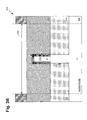
Figure 3A illustrates a cross-sectional view of a potion of an exemplary wafer during processing. -
Figure 3B illustrates a cross-sectional view of a potion of an exemplary wafer during processing. -
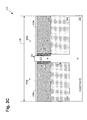
Figure 3C illustrates a cross-sectional view of a potion of an exemplary wafer during processing. -
Figure 4A illustrates a top view of a dual anti-fuse structure. -
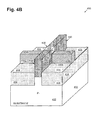
Figure 4B illustrates a perspective view of a dual anti-fuse structure. - The following description contains specific information pertaining to implementations in the present disclosure. The drawings in the present application and their accompanying detailed description are directed to merely exemplary implementations. Unless noted otherwise, like or corresponding elements among the figures may be indicated by like or corresponding reference numerals. Moreover, the drawings and illustrations in the present application are generally not to scale, and are not intended to correspond to actual relative dimensions.
-
Figure 1 illustrates a schematic diagram of acircuit 100 including a dualanti-fuse structure 150. The dualanti-fuse structure 150 includes an anti-fuse 102a and an anti-fuse 102b. - The anti-fuse 102a includes a
source 104a, adrain 106a, aprogrammable gate 108a, and achannel 110a. Initially, theprogrammable gate 108a and thechannel 110a form a high-resistance path for current flow. Thesource 104a and thedrain 106a can be coupled to the high-resistance path through thechannel 110a, as shown inFigure 1 . The anti-fuse 102a can be programmed by applying a programming voltage across theprogrammable gate 108a and thechannel 110a so as cause breakdown of a gate dielectric in theprogrammable gate 108a. Once programmed, the high-resistance path changes from to a low-resistance path to facilitate current flow. - Similarly, the anti-fuse 102b includes a
source 104b, adrain 106b, aprogrammable gate 108b, and achannel 110b. Initially, theprogrammable gate 108b and thechannel 110b form a high-resistance path for current flow. Thesource 104b and thedrain 106b can be coupled to the high-resistance path through thechannel 110b, as shown inFigure 1 . The anti-fuse 102b can be programmed by applying a programming voltage across theprogrammable gate 108b and thechannel 110b so as cause breakdown of a gate dielectric in theprogrammable gate 108b. Once programmed, the high-resistance path changes from to a low-resistance path to facilitate current flow. - In the dual
anti-fuse structure 150, thesource 104a of the anti-fuse 102a is coupled to thesource 104b of the anti-fuse 102b. Furthermore, in the dualanti-fuse structure 150, thedrain 106a of the anti-fuse 102a is coupled to thedrain 106b of the anti-fuse 102b. However, in some implementations, thesource 104a is not coupled to thesource 104b and/or thedrain 106a is not coupled to thedrain 106b in the dualanti-fuse structure 150. - The dual
anti-fuse structure 150 can have many different configurations and can be utilized in many different circuits. Thecircuit 100 illustrates ones such circuit utilizing the dual-anti-fuse structure 150. In thecircuit 100, theprogrammable gate 108a is coupled between aprogram transistor 114a and aread transistor 116a. Similarly, theprogrammable gate 108b is coupled between a program transistor 114b and a read transistor 116b. Thesource 104a and thesource 104b are coupled to a ground G1. Also, thedrain 106a and thedrain 106b are coupled to a ground G2, which can be the same as the ground G1. - In the
circuit 100, the anti-fuse 102a can be programmed by, for example, applying a programming voltage VPP1 across theprogrammable gate 108a and thechannel 110a through theprogram transistor 114a, which can be controlled by agate 120a. The programming voltage VPP1 is sufficient to program the anti-fuse 102a by blowing the anti-fuse 102a. The anti-fuse 102a can be read from by, for example, applying a read voltage VDD1 to theprogrammable gate 108a through theread transistor 116a, which can be controlled by agate 122a. The read voltage VDD1 can then be utilized to sense whether or not the anti-fuse 102a has been programmed based on the resistivity of theprogrammable gate 108a. - Similarly, in the
circuit 100, the anti-fuse 102b can be programmed by, for example, applying a programming voltage VPP2 across theprogrammable gate 108b and thechannel 110b through the program transistor 114b, which can be controlled by agate 120b. The programming voltage VPP2 is sufficient to program the anti-fuse 102b by blowing the anti-fuse 102b. The anti-fuse 102b can be read from by, for example, applying a read voltage VDD2 to theprogrammable gate 108b through the read transistor 116b, which can be controlled by agate 122b. The read voltage VDD2 can then be utilized to sense whether or not the anti-fuse 102b has been programmed based on the resistivity of theprogrammable gate 108b. - Thus, the dual-
anti fuse structure 150 includes the anti-fuse 102a and the anti-fuse 102b, which can optionally be independently operated as described above. The anti-fuse 102a described above includes thesource 104a and thedrain 106a for connection to the anti-fuse 102a. However, in some implementations, thesource 104a and/or thedrain 106a are not included in the dualanti-fuse structure 150 or are not utilized for connection to the anti-fuse 102a. For example, it will be appreciated that the anti-fuse 102a can include thesource 104a without thedrain 106a or can include thedrain 106a without thesource 104a. Similarly, the anti-fuse 102b described above includes thesource 104b and thedrain 106b for connection to the anti-fuse 102b. However, in some implementations, thesource 104b and/or thedrain 106b are not included in the dualanti-fuse structure 150 or are not utilized for connection to the anti-fuse 102b. For example, it will be appreciated that the anti-fuse 102b can include thesource 104b without thedrain 106b or can include thedrain 106b without thesource 104b. However, utilizing thesources drains -
Figure 2 shows a process flow diagram illustrating aprocess 200 for fabricating a dual anti-fuse structure, such as the dualanti-fuse structure 150 inFigure 1 . It is noted that the dualanti-fuse structure 150, as well as other dual anti-fuse structures in accordance with the present disclosure, can be fabricated utilizing processes other than theprocess 200. Also, while applicable for fabricating various dual anti-fuse structures, for illustrative purposes, theprocess 200 is described with respect toFigures 3A ,3B , and3C . The implementation illustrated by theprocess 200 can be performed on a processed wafer, which prior to theprocess 200 may include a substrate having a source region, a drain region, and a channel region in a common semiconductor fin, a gate dielectric layer, and a field dielectric layer. - Referring now to
Figure 2 andFigure 3A , theprocess 200 includes forming a conductive gate layer (e.g., 328) over a common semiconductor fin (e.g., 330) (270 inFigure 2 ). -
Figure 3A illustrates a cross-sectional view of a potion of awafer 370 during processing. As shown inFigure 3A , thewafer 370 includes asubstrate 332, afield dielectric layer 334, acommon semiconductor fin 330, a gate dielectric layer 340, and aconductive gate layer 328. - In the
wafer 370, thesubstrate 332 includes semiconductor material, such as single-crystal semiconductor material. In the present implementation, thesubstrate 332 is a silicon substrate and more particularly monocrystalline silicon. In the implementation shown, thesubstrate 332 is a P type substrate (e.g. a lightly doped P- substrate). It is noted that in other implementations, thesubstrate 332 is an N type (e.g. a lightly doped N-substrate) substrate or is undoped. Also, in other implementations, thesubstrate 332 is a semiconductor on insulator substrate, such as a silicon on insulator substrate (SOI) (Not shown). - The
common semiconductor fin 330 includes semiconductor material, and in the present implementation is silicon. Thecommon semiconductor fin 330 is formed in and on thesubstrate 332 and includeschannels common channel region 310. Thecommon channel region 310 is a doped region of thecommon semiconductor fin 330. In the present implementation, thecommon channel region 310 is P type (e.g., lightly doped P-). However, thecommon channel region 310 can be doped differently than what is shown inFigure 3A . In some implementations, for example, thecommon channel region 310 is N type (e.g., lightly doped N-). In the present implementation, thecommon channel region 310 has a similar doping profile as thesubstrate 332 as thecommon channel region 310 is formed from thesubstrate 332, however, thecommon channel region 310 can have a different doping profile than thesubstrate 332. Furthermore, while in the present implementation, thechannels common channel region 310, in some implementations, thechannels - Also in the implementation shown, the
field dielectric layer 334 is situated over thesubstrate 332. Thefield dielectric layer 334 includes one or more dielectric materials, such as silicon dioxide. In the present implementation, thefield dielectric layer 334 is a shallow trench isolation (STI) layer and underlies theconductive gate layer 328 and the gate dielectric layer 340. - The gate dielectric layer 340 is situated over and on the
substrate 332, thecommon semiconductor fin 330, and thefield dielectric layer 334. The gate dielectric layer 340 includes dielectric material. Dielectric material suitable for the gate dielectric layer 340 includes gate dielectric material for field-effect transistors (FETs), such as finFETs. In the present implementation, the gate dielectric layer 340 includes high-k dielectric material. Examples of high-k dielectric material for the gate dielectric layer 340 includes, as specific examples, hafnium oxide (HfO2), zirconium oxide (ZrO2), chromium oxide (CrO2), and the like. - The
conductive gate layer 328 is situated over thesubstrate 332 and on the gate dielectric layer 340 and thefield dielectric layer 334. Theconductive gate layer 328 includes conductive material. Conductive material suitable for theconductive gate layer 328 includes gate material for FETs, such as finFETs. In the present implementation, theconductive gate layer 328 includes metal, such as high-k metal gate material. Examples of high-k metal gate material for theconductive gate layer 328 include, as specific examples, tantalum (Ta), tantalum nitride (TaN), titanium nitride (TiN), molybdenum (Mo), ruthenium (Ru), tantalum carbide nitride (TaCN), or other metal or metal stack. - The
conductive gate layer 328 is formed over thecommon semiconductor fin 330. Prior to forming theconductive gate layer 328, thewafer 370 may also include thefield dielectric layer 334, the gate dielectric layer 340, and thecommon channel region 310 and common source and drain regions in the common semiconductor fin 330 (the common source and drain regions are not shown inFigure 3A ). Theconductive gate layer 328 can be formed over thecommon semiconductor fin 330 by depositing one or more layers of conductive material, such as metal, over thecommon semiconductor fin 330. The deposition can utilize physical vapor deposition (PVD), chemical vapor deposition (CVD), or another deposition technique. The deposited one or more layers of conductive material can then be planarized utilizing chemical mechanical planarization (CMP) or another planarization technique, resulting in thewafer 370 shown inFigure 3A . - Referring now to
Figure 2 andFigure 3B , theprocess 200 includes forming a mask (e.g., 344) over the conductive gate layer (e.g., 328) (272 inFigure 2 ). -
Figure 3B illustrates a cross-sectional view of a potion awafer 372 during processing. As shown inFigure 3B , thewafer 372 includes amask 344 formed over theconductive gate layer 328. Themask 344 exposes aregion 336 of theconductive gate layer 328 that overlies thecommon semiconductor fin 330. Themask 344 can include photoresist. Themask 344 can be formed over theconductive gate layer 328 by applying the photoresist to thewafer 370 ofFigure 3A over theconductive gate layer 328. The photoresist can be patterned to expose theregion 336 of theconductive gate layer 328, resulting in thewafer 372 shown inFigure 3B . - Referring now to
Figure 2 andFigure 3C , theprocess 200 includes etching the conductive gate layer (e.g., 328) using the mask (e.g., 344) to form a first programmable gate (e.g., 308a) of a first anti-fuse (e.g., 302a) and a second programmable gate (e.g., 308b) of a second anti-fuse (e.g., 302b) (274 inFigure 2 ). -
Figure 3C illustrates a cross-sectional view of a potion awafer 374 during processing. It is noted thatFigure 3C shows only theregion 336 for clarity. Thewafer 374 includes an anti-fuse 302a and an anti-fuse 302b. The anti-fuse 302a includes aprogrammable gate 308a and the anti-fuse 302b includes aprogrammable gate 308b. Theprogrammable gate 308a includes an electrode 328a and agate dielectric 340a. Thegate dielectric 340a is in contact with thechannel 310a. Theprogrammable gate 308b includes anelectrode 328b and a gate dielectric 340b. The gate dielectric 340b is in contact with thechannel 310b. - The
programmable gate 308a and theprogrammable gate 308b can be formed by etching theconductive gate layer 328 of thewafer 372 inFigure 3B using themask 344 of thewafer 372. The etching forms theprogrammable gates conductive gate layer 328 thereby forming theelectrodes 328a and 328b. Subsequently, themask 344 can be removed, resulting in thewafer 374 shown inFigure 3C . The etching of theconductive gate layer 328 can also optionally remove a portion of the gate dielectric layer 340 to form thegate dielectrics 340a and 340b. However in some implementations, a dedicated etch can be employed to remove the portion of the gate dielectric layer 340 to form thegate dielectrics 340a and 340b. Furthermore, in some implementations, the portion of the gate dielectric layer 340 may not be etched. For example, the gate dielectric layer 340 can remain covering thecommon semiconductor fin 330 as in thewafer 372. - Additional processing can be performed on the
wafer 374 including formation of contacts and silicide for the contacts. Thus, theprocess 200 provides for fabrication of dual anti-fuse structure. Theprocess 200 can be integrated into processes for fabrication of one or more finFETs. In some implementations, this integration only requires an addition of themask 344 for etching theconductive gate layer 328. However, themask 344 may also be utilized for fabricating finFETs or other components. -
Figure 4A illustrates a top view of a dualanti-fuse structure 450.Figure 4B illustrates a perspective view of the dualanti-fuse structure 450. The dualanti-fuse structure 450 corresponds to the dualanti-fuse structure 150 inFigure 1 . Furthermore, the dualanti-fuse structure 450 corresponds to theregion 336 of thewafer 374 inFigure 3C alongcross-section 3C-3C inFigure 4A . - The dual
anti-fuse structure 450 includes an anti-fuse 402a and an anti-fuse 402b corresponding respectively to the anti-fuse 102a and the anti-fuse 102b inFigure 1 and the anti-fuse 302a and the anti-fuse 302b inFigure 3C . The dualanti-fuse structure 450 further includes asubstrate 432, acommon semiconductor fin 430, acommon channel region 410, and afield dielectric layer 434 corresponding respectively to thesubstrate 332, thecommon semiconductor fin 330, thecommon channel region 310, and thefield dielectric layer 334 inFigure 3C . - The anti-fuse 402a includes a
channel 410a, asource 404a, adrain 406a, and aprogrammable gate 408a. Thechannel 410a, thesource 404a, thedrain 406a, and theprogrammable gate 408a correspond respectively to thechannel 110a, thesource 104a, thedrain 106a, and theprogrammable gate 108a inFigure 1 . Thechannel 410a further corresponds to thechannel 310a inFigure 3C . Also, while not shown inFigure 3C , thesource 404a and thedrain 406a can have corresponding constituents in thewafer 374 inFigure 3C , which can be in thecommon semiconductor fin 330 prior to forming thewafer 370 inFigure 3A . Theprogrammable gate 408a includes agate dielectric 440a and anelectrode 428a corresponding respectively to thegate dielectric 340a and the electrode 328a inFigure 3C . - Similarly, the anti-fuse 402b includes a
channel 410b, asource 404b, adrain 406b, and aprogrammable gate 408b. Thechannel 410b, thesource 404b, thedrain 406b, and theprogrammable gate 408b correspond respectively to thechannel 110b, thesource 104b, thedrain 106b, and theprogrammable gate 108b inFigure 1 . Thechannel 410b further corresponds to thechannel 310b inFigure 3C . Also, while not shown inFigure 3C , thesource 404b and thedrain 406b can have corresponding constituents in thewafer 374 inFigure 3C , which can be in thecommon semiconductor fin 330 prior to forming thewafer 370 inFigure 3A . Theprogrammable gate 408b includes a gate dielectric 440b and anelectrode 428b corresponding respectively to the gate dielectric 340b and theelectrode 328b inFigure 3C . - In the present implementation, the
sources common source region 404. Thecommon source region 404 is a doped region of thecommon semiconductor fin 430. In the present implementation, thecommon source region 404 is N type (e.g., highly doped N+). However, thecommon source region 404 can be doped differently than what is shown inFigures 4A and4B . In some implementations, for example, thecommon source region 404 is P type (e.g., highly doped P+). While in the present implementation, thesources common source region 404, in some implementations, thesources - Similarly, the
drains common drain region 406. Thecommon drain region 406 is a doped region of thecommon semiconductor fin 430. In the present implementation, thecommon drain region 406 is N type (e.g., highly doped N+). However, thecommon drain region 406 can be doped differently than what is shown inFigures 4A and4B . In some implementations, for example, thecommon drain region 406 is P type (e.g., highly doped P+). While in the present implementation, thedrains common drain region 406, in some implementations, thedrains sources drains - Thus, the dual
anti-fuse structure 450 includes thechannels sources drains common semiconductor fin 430. The thecommon source region 404 and thecommon drain region 406 can optionally be be formed concurrently with a source region and a drain region of a finFET. Also, thecommon channel region 410 can optionally be formed concurrently with a channel region of the finFET. As such, thecommon source region 404, thecommon source region 404, and thecommon drain region 406 may be integrated into a process for fabricating a finFET wiothout requiring additional processing steps. - The
channel 410a in thecommon semiconductor fin 430 is adjacent to theprogrammable gate 408a. Theprogrammable gate 408a is on asidewall 446a of thecommon semiconductor fin 430. The anti-fuse 402a is formed between thechannel 410a and theprogrammable gate 408a. Thechannel 410b in thecommon semiconductor fin 430 is adjacent to theprogrammable gate 408b. Theprogrammable gate 408b is on asidewall 446b of thecommon semiconductor fin 430. The anti-fuse 402b is formed between thechannel 410b and theprogrammable gate 408b. - Various configurations of the dual
anti-fuse structure 450 allow for the anti-fuse 402a and the anti-fuse 402b to be programmed. The anti-fuse 402a can be programmed, for example, by applying a programming voltage across theprogrammable gate 408a and thechannel 410a so as cause breakdown of thegate dielectric 440a in theprogrammable gate 408a. For example, thesource 404a and/or thedrain 406a can be coupled to ground and a programming voltage can be applied to theelectrode 428a to breakdown thegate dielectric 440a. Once programmed, theelectrode 428a has a low resistance path to a diode and/or diodes formed by thechannel 410a and thesource 404a and/or thechannel 410a and thedrain 406a. Utilizing both thesource 404a and thedrain 406a for connection to the anti-fuse 402a offers a low resistivity current path, however, it will be appreciated that the anti-fuse 402a can function with only one of thesource 404a and thedrain 406a. Thus, some implementations may not include one of thesource 404a and thedrain 406a or may not connect to one of thesource 404a and thedrain 406a. - Similarly, the anti-fuse 402b can be programmed by applying a programming voltage across the
programmable gate 408b and thechannel 410b so as cause breakdown of the gate dielectric 440b in theprogrammable gate 408b. For example, thesource 404b and/or thedrain 406b can be coupled to ground and a programming voltage can be applied to theelectrode 428b to breakdown thegate dielectric 440b. Once programmed, theelectrode 428b has a low resistance path to a diode and/or diodes formed by thechannel 410b and thesource 404b and/or thechannel 410b and thedrain 406b. Utilizing both thesource 404b and thedrain 406b for connection to the anti-fuse 402b offers a low resistivity current path, however, it will be appreciated that the anti-fuse 402b can function with only one of thesource 404b and thedrain 406b. Thus, some implementations may not include one of thesource 404b and thedrain 406b or may not connect to one of thesource 404b and thedrain 406b. - By including the
channel 410a and thechannel 410b in thecommon semiconductor fin 430, the dualanti-fuse structure 450 provides for the anti-fuse 402a and the anti-fuse 402b being compact while still being capable of independent operation. Thechannels programmable gate 408a and theprogrammable gate 408b. Additionally, thechannels source 404a and thedrain 406a and also are each situated between thesource 404b and thedrain 406b. Utilizing such an arrangement allows for, among other advantages, further compactness of the dualanti-fuse structure 450 as well as concurrent fabrication of the anti-fuses 402a and 402b. - From the above description it is manifest that various techniques can be used for implementing the concepts described in the present application without departing from the scope of those concepts. Moreover, while the concepts have been described with specific reference to certain implementations, a person of ordinary skill in the art would recognize that changes can be made in form and detail without departing from the scope of those concepts. As such, the described implementations are to be considered in all respects as illustrative and not restrictive. It should also be understood that the present application is not limited to the particular implementations described above, but many rearrangements, modifications, and substitutions are possible without departing from the scope of the present disclosure.
Claims (15)
- A dual anti-fuse structure comprising:a first channel in a common semiconductor fin adjacent to a first programmable gate;a second channel in said common semiconductor fin adjacent to a second programmable gate;a first anti-fuse formed between said first channel and said first programmable gate;a second anti-fuse formed between said second channel and said second programmable gate.
- The dual anti-fuse structure of claim 1, wherein said first programmable gate is on a first sidewall of said common semiconductor fin.
- The dual anti-fuse structure of claim 1 or 2, wherein said second programmable gate is on a second sidewall of said common semiconductor fin.
- The dual anti-fuse structure of any preceding claim, wherein said first programmable gate comprises a first gate dielectric and a first electrode.
- The dual anti-fuse structure of any preceding claim, wherein said first programmable gate comprises a second gate dielectric and a second electrode.
- The dual anti-fuse structure of any preceding claim, wherein said first anti-fuse comprises a first source and a first drain situated in said common semiconductor fin.
- The dual anti-fuse structure of any preceding claim, wherein said second anti-fuse comprises a second source and a second drain situated in said common semiconductor fin.
- The dual anti-fuse structure of any preceding claim, wherein said first channel is situated between said first programmable gate and said second programmable gate.
- The dual anti-fuse structure of any preceding claim, wherein said second channel is situated between said first programmable gate and said second programmable gate.
- The dual anti-fuse structure of any preceding claim, wherein said first channel and said second channel are situated in a common channel region.
- The dual anti-fuse structure of any preceding claim, wherein the first anti-fuse includes the first channel, a first source, and a first drain.
- The dual anti-fuse structure of any preceding claim, wherein the second anti-fuse includes the second channel, a second source, and a second drain.
- A dual anti-fuse structure comprising:a first anti-fuse including a first channel, a first source, and a first drain situated in a common semiconductor fin;a second anti-fuse including a second channel, a second source, and a second drain situated in said common semiconductor fin;said first anti-fuse formed between said first channel and a first programmable gate;said second anti-fuse formed between said second channel and a second programmable gate.
- The dual anti-fuse structure of claim 13, wherein said first source and said second source are situated in a common source region.
- The dual anti-fuse structure of claim 13 or 14, wherein said first drain and said second drain are situated in a common drain region.
Applications Claiming Priority (1)
| Application Number | Priority Date | Filing Date | Title |
|---|---|---|---|
| US13/548,123 US9536883B2 (en) | 2012-07-12 | 2012-07-12 | Dual anti-fuse |
Publications (3)
| Publication Number | Publication Date |
|---|---|
| EP2685498A2 true EP2685498A2 (en) | 2014-01-15 |
| EP2685498A3 EP2685498A3 (en) | 2017-07-12 |
| EP2685498B1 EP2685498B1 (en) | 2019-10-16 |
Family
ID=48747883
Family Applications (1)
| Application Number | Title | Priority Date | Filing Date |
|---|---|---|---|
| EP13003395.4A Active EP2685498B1 (en) | 2012-07-12 | 2013-07-04 | Dual anti-fuse |
Country Status (5)
| Country | Link |
|---|---|
| US (1) | US9536883B2 (en) |
| EP (1) | EP2685498B1 (en) |
| KR (1) | KR20140009063A (en) |
| CN (1) | CN103545291B (en) |
| TW (1) | TWI512947B (en) |
Cited By (1)
| Publication number | Priority date | Publication date | Assignee | Title |
|---|---|---|---|---|
| EP3945570A1 (en) * | 2020-07-31 | 2022-02-02 | Taiwan Semiconductor Manufacturing Co., Ltd. | Fuse cell structure |
Families Citing this family (12)
| Publication number | Priority date | Publication date | Assignee | Title |
|---|---|---|---|---|
| FR2993389B1 (en) * | 2012-07-10 | 2015-02-27 | Soitec Silicon On Insulator | antifuse |
| KR102212151B1 (en) * | 2014-02-11 | 2021-02-04 | 인텔 코포레이션 | Antifuse structure, antifuse bit cell structure, method of fabricating an antifuse structure, and method of forming a monolithic antifuse bit cell |
| KR102150869B1 (en) * | 2014-04-03 | 2020-09-02 | 삼성전자 주식회사 | fuse structure and semiconductor device including the same |
| KR102179169B1 (en) | 2014-09-02 | 2020-11-18 | 삼성전자주식회사 | Semiconductor device and method for manufacturing semiconductor device |
| KR102369926B1 (en) | 2015-04-10 | 2022-03-04 | 에스케이하이닉스 주식회사 | Anti-fuse, anti-fuse array and method of operating the same |
| CN106653737B (en) * | 2015-11-02 | 2019-10-15 | 中国科学院微电子研究所 | Anti-fuse structure and manufacturing method thereof |
| US9667251B1 (en) | 2016-01-29 | 2017-05-30 | Avago Technologies General Ip (Singapore) Pte. Ltd. | Charge steering latch for low soft error rate |
| US10008507B2 (en) | 2016-04-14 | 2018-06-26 | International Business Machines Corporation | Metal FinFET anti-fuse |
| US10090027B2 (en) * | 2016-05-25 | 2018-10-02 | Ememory Technology Inc. | Memory system with low read power |
| US9831254B1 (en) | 2016-09-22 | 2017-11-28 | International Business Machines Corporation | Multiple breakdown point low resistance anti-fuse structure |
| CN115377058A (en) * | 2021-05-20 | 2022-11-22 | 长鑫存储技术有限公司 | Fuse structure and manufacturing method thereof |
| US20260047085A1 (en) * | 2024-08-12 | 2026-02-12 | Globalfoundries U.S. Inc. | Memory cell including dual-antifuse device, memory structure, and operating method |
Family Cites Families (7)
| Publication number | Priority date | Publication date | Assignee | Title |
|---|---|---|---|---|
| WO2004059726A1 (en) * | 2002-12-20 | 2004-07-15 | International Business Machines Corporation | Integrated antifuse structure for finfet and cmos devices |
| KR100781615B1 (en) | 2005-05-30 | 2007-12-07 | 인터내셔널 비지네스 머신즈 코포레이션 | Integrated Anti-Fuse Architecture for FINEFET and CMOS Devices |
| US8274132B2 (en) * | 2008-02-14 | 2012-09-25 | Infineon Technologies Ag | Electrical device and fabrication method |
| JP2010034266A (en) * | 2008-07-29 | 2010-02-12 | Renesas Technology Corp | Double gate semiconductor device and method of manufacturing the same |
| US8305790B2 (en) * | 2009-03-16 | 2012-11-06 | Taiwan Semiconductor Manufacturing Company, Ltd. | Electrical anti-fuse and related applications |
| KR101752151B1 (en) * | 2010-08-27 | 2017-06-30 | 삼성전자주식회사 | Fuse circuit, fuse array, semiconductor memory device including the same and a method of manufacturing semiconductor device |
| US9159734B2 (en) * | 2011-10-18 | 2015-10-13 | Intel Corporation | Antifuse element utilizing non-planar topology |
-
2012
- 2012-07-12 US US13/548,123 patent/US9536883B2/en not_active Expired - Fee Related
-
2013
- 2013-07-04 EP EP13003395.4A patent/EP2685498B1/en active Active
- 2013-07-08 CN CN201310285046.8A patent/CN103545291B/en active Active
- 2013-07-08 TW TW102124356A patent/TWI512947B/en not_active IP Right Cessation
- 2013-07-12 KR KR1020130081946A patent/KR20140009063A/en not_active Ceased
Cited By (1)
| Publication number | Priority date | Publication date | Assignee | Title |
|---|---|---|---|---|
| EP3945570A1 (en) * | 2020-07-31 | 2022-02-02 | Taiwan Semiconductor Manufacturing Co., Ltd. | Fuse cell structure |
Also Published As
| Publication number | Publication date |
|---|---|
| EP2685498B1 (en) | 2019-10-16 |
| CN103545291B (en) | 2017-05-31 |
| US20140015095A1 (en) | 2014-01-16 |
| KR20140009063A (en) | 2014-01-22 |
| TWI512947B (en) | 2015-12-11 |
| CN103545291A (en) | 2014-01-29 |
| EP2685498A3 (en) | 2017-07-12 |
| US9536883B2 (en) | 2017-01-03 |
| TW201419498A (en) | 2014-05-16 |
Similar Documents
| Publication | Publication Date | Title |
|---|---|---|
| EP2685498B1 (en) | Dual anti-fuse | |
| JP4790967B2 (en) | Dual metal gate transistor for CMOS process | |
| US6794281B2 (en) | Dual metal gate transistors for CMOS process | |
| US9443991B2 (en) | Semiconductor device and method of manufacturing the same | |
| US8803253B2 (en) | Replacement metal gate process for CMOS integrated circuits | |
| US8298882B2 (en) | Metal gate and high-K dielectric devices with PFET channel SiGe | |
| US9972545B2 (en) | System and method for a field-effect transistor with dual vertical gates | |
| US10043881B2 (en) | Semiconductor device and method of manufacturing the same | |
| US8816421B2 (en) | Semiconductor device with semiconductor fins and floating gate | |
| US20190043963A1 (en) | Transistor element with gate electrode of reduced height and raised drain and source regions and method of fabricating the same | |
| CN102683343A (en) | Semiconductor device and method of manufacturing the same | |
| US20050205938A1 (en) | Semiconductor device and method of manufacture the same | |
| US20090224324A1 (en) | Semiconductor device and manufacturing method thereof | |
| TWI555206B (en) | Integrated circuit and method for fabricating the same | |
| CN206584930U (en) | Integrated circuit | |
| US11742199B2 (en) | Semiconductor device and method of manufacturing the same | |
| HK1191448A (en) | Dual anti-fuse | |
| JP4011014B2 (en) | Semiconductor device and manufacturing method thereof | |
| CN114334903A (en) | Semiconductor device and method for manufacturing semiconductor device |
Legal Events
| Date | Code | Title | Description |
|---|---|---|---|
| PUAI | Public reference made under article 153(3) epc to a published international application that has entered the european phase |
Free format text: ORIGINAL CODE: 0009012 |
|
| 17P | Request for examination filed |
Effective date: 20130704 |
|
| AK | Designated contracting states |
Kind code of ref document: A2 Designated state(s): AL AT BE BG CH CY CZ DE DK EE ES FI FR GB GR HR HU IE IS IT LI LT LU LV MC MK MT NL NO PL PT RO RS SE SI SK SM TR |
|
| AX | Request for extension of the european patent |
Extension state: BA ME |
|
| PUAL | Search report despatched |
Free format text: ORIGINAL CODE: 0009013 |
|
| STAA | Information on the status of an ep patent application or granted ep patent |
Free format text: STATUS: EXAMINATION IS IN PROGRESS |
|
| RIC1 | Information provided on ipc code assigned before grant |
Ipc: H01L 27/10 20060101AFI20170601BHEP Ipc: H01L 27/112 20060101ALI20170601BHEP Ipc: H01L 23/525 20060101ALI20170601BHEP |
|
| AK | Designated contracting states |
Kind code of ref document: A3 Designated state(s): AL AT BE BG CH CY CZ DE DK EE ES FI FR GB GR HR HU IE IS IT LI LT LU LV MC MK MT NL NO PL PT RO RS SE SI SK SM TR |
|
| AX | Request for extension of the european patent |
Extension state: BA ME |
|
| RAP1 | Party data changed (applicant data changed or rights of an application transferred) |
Owner name: AVAGO TECHNOLOGIES GENERAL IP (SINGAPORE) PTE. LTD |
|
| 17Q | First examination report despatched |
Effective date: 20170629 |
|
| RBV | Designated contracting states (corrected) |
Designated state(s): AL AT BE BG CH CY CZ DE DK EE ES FI FR GB GR HR HU IE IS IT LI LT LU LV MC MK MT NL NO PL PT RO RS SE SI SK SM TR |
|
| RAP1 | Party data changed (applicant data changed or rights of an application transferred) |
Owner name: AVAGO TECHNOLOGIES INTERNATIONAL SALES PTE. LIMITE |
|
| GRAP | Despatch of communication of intention to grant a patent |
Free format text: ORIGINAL CODE: EPIDOSNIGR1 |
|
| STAA | Information on the status of an ep patent application or granted ep patent |
Free format text: STATUS: GRANT OF PATENT IS INTENDED |
|
| INTG | Intention to grant announced |
Effective date: 20190509 |
|
| GRAS | Grant fee paid |
Free format text: ORIGINAL CODE: EPIDOSNIGR3 |
|
| GRAA | (expected) grant |
Free format text: ORIGINAL CODE: 0009210 |
|
| STAA | Information on the status of an ep patent application or granted ep patent |
Free format text: STATUS: THE PATENT HAS BEEN GRANTED |
|
| AK | Designated contracting states |
Kind code of ref document: B1 Designated state(s): AL AT BE BG CH CY CZ DE DK EE ES FI FR GB GR HR HU IE IS IT LI LT LU LV MC MK MT NL NO PL PT RO RS SE SI SK SM TR |
|
| REG | Reference to a national code |
Ref country code: GB Ref legal event code: FG4D |
|
| REG | Reference to a national code |
Ref country code: DE Ref legal event code: R096 Ref document number: 602013061690 Country of ref document: DE Ref country code: CH Ref legal event code: EP |
|
| REG | Reference to a national code |
Ref country code: IE Ref legal event code: FG4D |
|
| REG | Reference to a national code |
Ref country code: AT Ref legal event code: REF Ref document number: 1192132 Country of ref document: AT Kind code of ref document: T Effective date: 20191115 |
|
| REG | Reference to a national code |
Ref country code: NL Ref legal event code: MP Effective date: 20191016 |
|
| REG | Reference to a national code |
Ref country code: LT Ref legal event code: MG4D |
|
| REG | Reference to a national code |
Ref country code: AT Ref legal event code: MK05 Ref document number: 1192132 Country of ref document: AT Kind code of ref document: T Effective date: 20191016 |
|
| PG25 | Lapsed in a contracting state [announced via postgrant information from national office to epo] |
Ref country code: NL Free format text: LAPSE BECAUSE OF FAILURE TO SUBMIT A TRANSLATION OF THE DESCRIPTION OR TO PAY THE FEE WITHIN THE PRESCRIBED TIME-LIMIT Effective date: 20191016 Ref country code: PL Free format text: LAPSE BECAUSE OF FAILURE TO SUBMIT A TRANSLATION OF THE DESCRIPTION OR TO PAY THE FEE WITHIN THE PRESCRIBED TIME-LIMIT Effective date: 20191016 Ref country code: SE Free format text: LAPSE BECAUSE OF FAILURE TO SUBMIT A TRANSLATION OF THE DESCRIPTION OR TO PAY THE FEE WITHIN THE PRESCRIBED TIME-LIMIT Effective date: 20191016 Ref country code: LV Free format text: LAPSE BECAUSE OF FAILURE TO SUBMIT A TRANSLATION OF THE DESCRIPTION OR TO PAY THE FEE WITHIN THE PRESCRIBED TIME-LIMIT Effective date: 20191016 Ref country code: GR Free format text: LAPSE BECAUSE OF FAILURE TO SUBMIT A TRANSLATION OF THE DESCRIPTION OR TO PAY THE FEE WITHIN THE PRESCRIBED TIME-LIMIT Effective date: 20200117 Ref country code: AT Free format text: LAPSE BECAUSE OF FAILURE TO SUBMIT A TRANSLATION OF THE DESCRIPTION OR TO PAY THE FEE WITHIN THE PRESCRIBED TIME-LIMIT Effective date: 20191016 Ref country code: NO Free format text: LAPSE BECAUSE OF FAILURE TO SUBMIT A TRANSLATION OF THE DESCRIPTION OR TO PAY THE FEE WITHIN THE PRESCRIBED TIME-LIMIT Effective date: 20200116 Ref country code: ES Free format text: LAPSE BECAUSE OF FAILURE TO SUBMIT A TRANSLATION OF THE DESCRIPTION OR TO PAY THE FEE WITHIN THE PRESCRIBED TIME-LIMIT Effective date: 20191016 Ref country code: LT Free format text: LAPSE BECAUSE OF FAILURE TO SUBMIT A TRANSLATION OF THE DESCRIPTION OR TO PAY THE FEE WITHIN THE PRESCRIBED TIME-LIMIT Effective date: 20191016 Ref country code: PT Free format text: LAPSE BECAUSE OF FAILURE TO SUBMIT A TRANSLATION OF THE DESCRIPTION OR TO PAY THE FEE WITHIN THE PRESCRIBED TIME-LIMIT Effective date: 20200217 Ref country code: FI Free format text: LAPSE BECAUSE OF FAILURE TO SUBMIT A TRANSLATION OF THE DESCRIPTION OR TO PAY THE FEE WITHIN THE PRESCRIBED TIME-LIMIT Effective date: 20191016 Ref country code: BG Free format text: LAPSE BECAUSE OF FAILURE TO SUBMIT A TRANSLATION OF THE DESCRIPTION OR TO PAY THE FEE WITHIN THE PRESCRIBED TIME-LIMIT Effective date: 20200116 |
|
| PG25 | Lapsed in a contracting state [announced via postgrant information from national office to epo] |
Ref country code: IS Free format text: LAPSE BECAUSE OF FAILURE TO SUBMIT A TRANSLATION OF THE DESCRIPTION OR TO PAY THE FEE WITHIN THE PRESCRIBED TIME-LIMIT Effective date: 20200224 Ref country code: RS Free format text: LAPSE BECAUSE OF FAILURE TO SUBMIT A TRANSLATION OF THE DESCRIPTION OR TO PAY THE FEE WITHIN THE PRESCRIBED TIME-LIMIT Effective date: 20191016 Ref country code: HR Free format text: LAPSE BECAUSE OF FAILURE TO SUBMIT A TRANSLATION OF THE DESCRIPTION OR TO PAY THE FEE WITHIN THE PRESCRIBED TIME-LIMIT Effective date: 20191016 |
|
| PG25 | Lapsed in a contracting state [announced via postgrant information from national office to epo] |
Ref country code: AL Free format text: LAPSE BECAUSE OF FAILURE TO SUBMIT A TRANSLATION OF THE DESCRIPTION OR TO PAY THE FEE WITHIN THE PRESCRIBED TIME-LIMIT Effective date: 20191016 |
|
| REG | Reference to a national code |
Ref country code: DE Ref legal event code: R097 Ref document number: 602013061690 Country of ref document: DE |
|
| PG2D | Information on lapse in contracting state deleted |
Ref country code: IS |
|
| PG25 | Lapsed in a contracting state [announced via postgrant information from national office to epo] |
Ref country code: EE Free format text: LAPSE BECAUSE OF FAILURE TO SUBMIT A TRANSLATION OF THE DESCRIPTION OR TO PAY THE FEE WITHIN THE PRESCRIBED TIME-LIMIT Effective date: 20191016 Ref country code: DK Free format text: LAPSE BECAUSE OF FAILURE TO SUBMIT A TRANSLATION OF THE DESCRIPTION OR TO PAY THE FEE WITHIN THE PRESCRIBED TIME-LIMIT Effective date: 20191016 Ref country code: CZ Free format text: LAPSE BECAUSE OF FAILURE TO SUBMIT A TRANSLATION OF THE DESCRIPTION OR TO PAY THE FEE WITHIN THE PRESCRIBED TIME-LIMIT Effective date: 20191016 Ref country code: RO Free format text: LAPSE BECAUSE OF FAILURE TO SUBMIT A TRANSLATION OF THE DESCRIPTION OR TO PAY THE FEE WITHIN THE PRESCRIBED TIME-LIMIT Effective date: 20191016 Ref country code: IS Free format text: LAPSE BECAUSE OF FAILURE TO SUBMIT A TRANSLATION OF THE DESCRIPTION OR TO PAY THE FEE WITHIN THE PRESCRIBED TIME-LIMIT Effective date: 20200216 |
|
| PLBE | No opposition filed within time limit |
Free format text: ORIGINAL CODE: 0009261 |
|
| STAA | Information on the status of an ep patent application or granted ep patent |
Free format text: STATUS: NO OPPOSITION FILED WITHIN TIME LIMIT |
|
| PG25 | Lapsed in a contracting state [announced via postgrant information from national office to epo] |
Ref country code: IT Free format text: LAPSE BECAUSE OF FAILURE TO SUBMIT A TRANSLATION OF THE DESCRIPTION OR TO PAY THE FEE WITHIN THE PRESCRIBED TIME-LIMIT Effective date: 20191016 Ref country code: SK Free format text: LAPSE BECAUSE OF FAILURE TO SUBMIT A TRANSLATION OF THE DESCRIPTION OR TO PAY THE FEE WITHIN THE PRESCRIBED TIME-LIMIT Effective date: 20191016 Ref country code: SM Free format text: LAPSE BECAUSE OF FAILURE TO SUBMIT A TRANSLATION OF THE DESCRIPTION OR TO PAY THE FEE WITHIN THE PRESCRIBED TIME-LIMIT Effective date: 20191016 |
|
| 26N | No opposition filed |
Effective date: 20200717 |
|
| PG25 | Lapsed in a contracting state [announced via postgrant information from national office to epo] |
Ref country code: SI Free format text: LAPSE BECAUSE OF FAILURE TO SUBMIT A TRANSLATION OF THE DESCRIPTION OR TO PAY THE FEE WITHIN THE PRESCRIBED TIME-LIMIT Effective date: 20191016 |
|
| PG25 | Lapsed in a contracting state [announced via postgrant information from national office to epo] |
Ref country code: MC Free format text: LAPSE BECAUSE OF FAILURE TO SUBMIT A TRANSLATION OF THE DESCRIPTION OR TO PAY THE FEE WITHIN THE PRESCRIBED TIME-LIMIT Effective date: 20191016 |
|
| REG | Reference to a national code |
Ref country code: CH Ref legal event code: PL |
|
| GBPC | Gb: european patent ceased through non-payment of renewal fee |
Effective date: 20200704 |
|
| REG | Reference to a national code |
Ref country code: BE Ref legal event code: MM Effective date: 20200731 |
|
| PG25 | Lapsed in a contracting state [announced via postgrant information from national office to epo] |
Ref country code: LU Free format text: LAPSE BECAUSE OF NON-PAYMENT OF DUE FEES Effective date: 20200704 Ref country code: FR Free format text: LAPSE BECAUSE OF NON-PAYMENT OF DUE FEES Effective date: 20200731 Ref country code: GB Free format text: LAPSE BECAUSE OF NON-PAYMENT OF DUE FEES Effective date: 20200704 Ref country code: IE Free format text: LAPSE BECAUSE OF NON-PAYMENT OF DUE FEES Effective date: 20200704 Ref country code: LI Free format text: LAPSE BECAUSE OF NON-PAYMENT OF DUE FEES Effective date: 20200731 Ref country code: CH Free format text: LAPSE BECAUSE OF NON-PAYMENT OF DUE FEES Effective date: 20200731 |
|
| PG25 | Lapsed in a contracting state [announced via postgrant information from national office to epo] |
Ref country code: BE Free format text: LAPSE BECAUSE OF NON-PAYMENT OF DUE FEES Effective date: 20200731 |
|
| PG25 | Lapsed in a contracting state [announced via postgrant information from national office to epo] |
Ref country code: TR Free format text: LAPSE BECAUSE OF FAILURE TO SUBMIT A TRANSLATION OF THE DESCRIPTION OR TO PAY THE FEE WITHIN THE PRESCRIBED TIME-LIMIT Effective date: 20191016 Ref country code: MT Free format text: LAPSE BECAUSE OF FAILURE TO SUBMIT A TRANSLATION OF THE DESCRIPTION OR TO PAY THE FEE WITHIN THE PRESCRIBED TIME-LIMIT Effective date: 20191016 Ref country code: CY Free format text: LAPSE BECAUSE OF FAILURE TO SUBMIT A TRANSLATION OF THE DESCRIPTION OR TO PAY THE FEE WITHIN THE PRESCRIBED TIME-LIMIT Effective date: 20191016 |
|
| PG25 | Lapsed in a contracting state [announced via postgrant information from national office to epo] |
Ref country code: MK Free format text: LAPSE BECAUSE OF FAILURE TO SUBMIT A TRANSLATION OF THE DESCRIPTION OR TO PAY THE FEE WITHIN THE PRESCRIBED TIME-LIMIT Effective date: 20191016 |
|
| REG | Reference to a national code |
Ref country code: DE Ref legal event code: R079 Ref document number: 602013061690 Country of ref document: DE Free format text: PREVIOUS MAIN CLASS: H01L0027100000 Ipc: H10D0084000000 |
|
| PGFP | Annual fee paid to national office [announced via postgrant information from national office to epo] |
Ref country code: DE Payment date: 20250710 Year of fee payment: 13 |