EP2684984A2 - Button or fastener member of copper-plated aluminum or aluminum alloy and method of production thereof - Google Patents
Button or fastener member of copper-plated aluminum or aluminum alloy and method of production thereof Download PDFInfo
- Publication number
- EP2684984A2 EP2684984A2 EP13003283.2A EP13003283A EP2684984A2 EP 2684984 A2 EP2684984 A2 EP 2684984A2 EP 13003283 A EP13003283 A EP 13003283A EP 2684984 A2 EP2684984 A2 EP 2684984A2
- Authority
- EP
- European Patent Office
- Prior art keywords
- plating layer
- copper plating
- copper
- button
- aluminum
- Prior art date
- Legal status (The legal status is an assumption and is not a legal conclusion. Google has not performed a legal analysis and makes no representation as to the accuracy of the status listed.)
- Granted
Links
Images


Classifications
-
- C—CHEMISTRY; METALLURGY
- C25—ELECTROLYTIC OR ELECTROPHORETIC PROCESSES; APPARATUS THEREFOR
- C25D—PROCESSES FOR THE ELECTROLYTIC OR ELECTROPHORETIC PRODUCTION OF COATINGS; ELECTROFORMING; APPARATUS THEREFOR
- C25D7/00—Electroplating characterised by the article coated
- C25D7/02—Slide fasteners
-
- C—CHEMISTRY; METALLURGY
- C25—ELECTROLYTIC OR ELECTROPHORETIC PROCESSES; APPARATUS THEREFOR
- C25D—PROCESSES FOR THE ELECTROLYTIC OR ELECTROPHORETIC PRODUCTION OF COATINGS; ELECTROFORMING; APPARATUS THEREFOR
- C25D17/00—Constructional parts, or assemblies thereof, of cells for electrolytic coating
- C25D17/16—Apparatus for electrolytic coating of small objects in bulk
-
- C—CHEMISTRY; METALLURGY
- C25—ELECTROLYTIC OR ELECTROPHORETIC PROCESSES; APPARATUS THEREFOR
- C25D—PROCESSES FOR THE ELECTROLYTIC OR ELECTROPHORETIC PRODUCTION OF COATINGS; ELECTROFORMING; APPARATUS THEREFOR
- C25D5/00—Electroplating characterised by the process; Pretreatment or after-treatment of workpieces
- C25D5/10—Electroplating with more than one layer of the same or of different metals
-
- C—CHEMISTRY; METALLURGY
- C25—ELECTROLYTIC OR ELECTROPHORETIC PROCESSES; APPARATUS THEREFOR
- C25D—PROCESSES FOR THE ELECTROLYTIC OR ELECTROPHORETIC PRODUCTION OF COATINGS; ELECTROFORMING; APPARATUS THEREFOR
- C25D5/00—Electroplating characterised by the process; Pretreatment or after-treatment of workpieces
- C25D5/34—Pretreatment of metallic surfaces to be electroplated
- C25D5/42—Pretreatment of metallic surfaces to be electroplated of light metals
- C25D5/44—Aluminium
-
- C—CHEMISTRY; METALLURGY
- C25—ELECTROLYTIC OR ELECTROPHORETIC PROCESSES; APPARATUS THEREFOR
- C25D—PROCESSES FOR THE ELECTROLYTIC OR ELECTROPHORETIC PRODUCTION OF COATINGS; ELECTROFORMING; APPARATUS THEREFOR
- C25D5/00—Electroplating characterised by the process; Pretreatment or after-treatment of workpieces
- C25D5/60—Electroplating characterised by the structure or texture of the layers
- C25D5/605—Surface topography of the layers, e.g. rough, dendritic or nodular layers
- C25D5/611—Smooth layers
-
- C—CHEMISTRY; METALLURGY
- C25—ELECTROLYTIC OR ELECTROPHORETIC PROCESSES; APPARATUS THEREFOR
- C25D—PROCESSES FOR THE ELECTROLYTIC OR ELECTROPHORETIC PRODUCTION OF COATINGS; ELECTROFORMING; APPARATUS THEREFOR
- C25D5/00—Electroplating characterised by the process; Pretreatment or after-treatment of workpieces
- C25D5/60—Electroplating characterised by the structure or texture of the layers
- C25D5/615—Microstructure of the layers, e.g. mixed structure
- C25D5/617—Crystalline layers
-
- C—CHEMISTRY; METALLURGY
- C25—ELECTROLYTIC OR ELECTROPHORETIC PROCESSES; APPARATUS THEREFOR
- C25D—PROCESSES FOR THE ELECTROLYTIC OR ELECTROPHORETIC PRODUCTION OF COATINGS; ELECTROFORMING; APPARATUS THEREFOR
- C25D7/00—Electroplating characterised by the article coated
-
- C—CHEMISTRY; METALLURGY
- C25—ELECTROLYTIC OR ELECTROPHORETIC PROCESSES; APPARATUS THEREFOR
- C25D—PROCESSES FOR THE ELECTROLYTIC OR ELECTROPHORETIC PRODUCTION OF COATINGS; ELECTROFORMING; APPARATUS THEREFOR
- C25D3/00—Electroplating: Baths therefor
- C25D3/02—Electroplating: Baths therefor from solutions
- C25D3/38—Electroplating: Baths therefor from solutions of copper
- C25D3/40—Electroplating: Baths therefor from solutions of copper from cyanide baths, e.g. with Cu+
-
- C—CHEMISTRY; METALLURGY
- C25—ELECTROLYTIC OR ELECTROPHORETIC PROCESSES; APPARATUS THEREFOR
- C25D—PROCESSES FOR THE ELECTROLYTIC OR ELECTROPHORETIC PRODUCTION OF COATINGS; ELECTROFORMING; APPARATUS THEREFOR
- C25D3/00—Electroplating: Baths therefor
- C25D3/02—Electroplating: Baths therefor from solutions
- C25D3/56—Electroplating: Baths therefor from solutions of alloys
- C25D3/58—Electroplating: Baths therefor from solutions of alloys containing more than 50% by weight of copper
-
- Y—GENERAL TAGGING OF NEW TECHNOLOGICAL DEVELOPMENTS; GENERAL TAGGING OF CROSS-SECTIONAL TECHNOLOGIES SPANNING OVER SEVERAL SECTIONS OF THE IPC; TECHNICAL SUBJECTS COVERED BY FORMER USPC CROSS-REFERENCE ART COLLECTIONS [XRACs] AND DIGESTS
- Y10—TECHNICAL SUBJECTS COVERED BY FORMER USPC
- Y10T—TECHNICAL SUBJECTS COVERED BY FORMER US CLASSIFICATION
- Y10T24/00—Buckles, buttons, clasps, etc.
- Y10T24/36—Button with fastener
-
- Y—GENERAL TAGGING OF NEW TECHNOLOGICAL DEVELOPMENTS; GENERAL TAGGING OF CROSS-SECTIONAL TECHNOLOGIES SPANNING OVER SEVERAL SECTIONS OF THE IPC; TECHNICAL SUBJECTS COVERED BY FORMER USPC CROSS-REFERENCE ART COLLECTIONS [XRACs] AND DIGESTS
- Y10—TECHNICAL SUBJECTS COVERED BY FORMER USPC
- Y10T—TECHNICAL SUBJECTS COVERED BY FORMER US CLASSIFICATION
- Y10T428/00—Stock material or miscellaneous articles
- Y10T428/12—All metal or with adjacent metals
- Y10T428/12493—Composite; i.e., plural, adjacent, spatially distinct metal components [e.g., layers, joint, etc.]
- Y10T428/12736—Al-base component
- Y10T428/1275—Next to Group VIII or IB metal-base component
Definitions
- This invention concerns a button or fastener member of copper-plated aluminum. Additionally, it concerns a production method for the aforementioned member.
- buttons and fasteners are conventionally known to be surface-plated using brass as a base metal due to its superior platability.
- Products in the fastener field are known to be surface-plated using zinc as a base metal.
- steep increases in the price of materials have posed a problem, in addition to a demand for lightweight buttons and fasteners. Therefore, the production of buttons and fasteners using aluminum, which is lightweight and relatively inexpensive, has been considered as a solution.
- surface plating is desirable.
- This invention was conceived out of consideration of the aforementioned facts, and one aspect consists of a button or fastener member wherein aluminum or an aluminum alloy is used as raw material, a first copper plating layer is formed directly over the entire surface of said raw material, and a second copper plating layer is formed directly on top of the first copper plating layer, with the aforementioned second copper plating layer being thicker than the aforementioned first copper plating layer.
- the mean crystal grain size of the first copper plating layer is larger than the mean crystal grain size of the second copper plating layer.
- the mean thickness of the first copper plating layer is 0.01-1.5 ⁇ m, while the mean thickness of second copper plating layer is 1.6-10 ⁇ m.
- a final plating layer is formed in one layer, or two or more layers, on top of the second copper plating layer.
- the overall thickness of the final plating layer is thinner than the total thickness of the first copper plating layer and second copper plating layer.
- the first copper plating layer and second copper plating layer are both formed by barrel plating.
- Another aspect of this invention is a button or fastener equipped with a button or fastener member based on this invention.
- a further aspect of this invention is a production method for a copper-plated button or fastener, consisting of: a first step to produce a semi-finished product for a button or fastener member by performing a forming process using aluminum or an aluminum alloy as raw material, a second step to form a first copper plating layer directly over the entire surface of the raw material through electric strike-plating copper onto semi-finished product obtained through step 1 with a barrel, and next, a third step to form a second copper plating layer thicker than the first copper plating layer, directly on top of the first copper plating layer, through electric-plating copper with a barrel.
- the mean crystal grain size of the first copper plating layer is larger than the mean crystal grain size of the second copper plating layer.
- the third step starts within one minute after the second step.
- the mean thickness of the first copper plating layer is 0.01-1.5 ⁇ m, while the mean thickness of second copper plating layer is 1.6-10 ⁇ m.
- a fourth step is further included to form a final plating layer in one layer, or two or more layers, on top of the second copper plating layer.
- the overall thickness of the final plating layer is thinner than the total thickness of the first copper plating layer and second copper plating layer.
- Fig. 1 An oblique drawing showing an example of a button fastener, which is a member of a snap button.
- Fig. 2 A cross sectional drawing of the button fastener in Fig. 1 and partial enlarged views thereof.
- Fig. 3 A cross sectional drawing showing the button fastener in Fig. 1 prior to fastening the button to cloth.
- Fig. 4 A cross sectional drawing showing the button fastened to cloth.
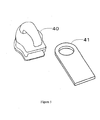
- Fig. 5 An oblique drawing of a slider body and pull tab for a slider fastener based on an embodiment of this invention.
- a button or fastener member based on this invention uses aluminum or an aluminum alloy as raw material.
- the aluminum alloy may be an aluminum-copper alloy, aluminum-manganese alloy, aluminum-silicon alloy, aluminum-magnesium alloy, aluminum-magnesium-silicon alloy, aluminum-zinc-magnesium alloy, aluminum-zinc-magnesium-copper alloy, or any other suitable aluminum alloy. Based on reasons of strength and workability, among these alloys, an aluminum-magnesium alloy, aluminum-manganese alloy or aluminum-magnesium-silicon alloy is preferred, ideally an aluminum-magnesium alloy.
- a button or fastener member based on this invention involves a first copper plating layer being formed as a base plating layer directly on top of the surface of the aforementioned raw material. Since adhesion decreases if the thickness of the first copper plating layer becomes too thin, a mean thickness of 0.01 ⁇ m or more is preferred, ideally a mean thickness of 0.1 ⁇ m or more. On the other hand, since production efficiency decreases if the thickness of the first copper plating layer is too thick, a mean thickness of 1.5 ⁇ m or less is preferred, ideally a mean thickness of 1.0 ⁇ m or less.
- the first copper plating layer is preferably formed after appropriate pretreatment is performed by degreasing, acid washing, washing with a surfactant or water washing.
- the product may be formed by performing a forming process using aluminum or an aluminum alloy as raw material and a method such as die-cast forming or press-forming. Then after the semi-finished product for a button or fastener member is formed, the first copper plating layer is formed by electric strike-plating copper onto this semi-finished product with a barrel.
- Barrel plating eliminates the need to set material into a jig for plating, and enables mass production, unlike still plating, and furthermore, eliminates concerns of corrosion due to contact traces left during setting of the material in a jig, since there is no such setting. Barrel plating allows plating of the entire surface of the product, whereas still plating leaves the portion of the surface covered by the jig un-plated.
- CL-NC ALKALINE COPPER method by Uyemura & Co., Ltd. (U.S.) is one preferred method due to its adhesion to substrate surfaces, uniform adhesion, and relative superiority in smoothness and other qualities.
- a cyanide-free bath is used for this plating bath, which allows for direct copper strike-plating on the surface of aluminum without zincate treatment.
- the CL-NC ALKALINE COPPER method makes it possible to simultaneously perform removal of oxide film formed on the raw material surface and copper plating, without zincate or other base treatment.
- a current density of 0.3-1.2 A/dm 2 is preferred, ideally 0.5-1.0 A/dm 2 .
- a plating bath temperature of 55-75°C is preferred, ideally 60-70°C.
- a pH of 7.0-8.5 is preferred, ideally 7.0-8.0.
- a plating time of 30-60 minutes is preferred, ideally 40-50 minutes.
- a barrel speed of 2-12 rpm is preferred, ideally 4-8 rpm.
- the second copper plating layer which is an intermediate plating layer, is formed directly on top of the first copper plating layer, with a larger thickness than the first copper plating layer.
- the merits of having a second copper plating layer thicker than the first copper plating layer are improved strength of the member itself, and improved durability against corrosion.
- the plating is smoother. Because of the high smoothness, luster is improved, and plating adhesion is improved when the top of the second copper plating layer receives an additional final plating.
- a mean thickness of 1.6 ⁇ m or more is preferred for the second copper plating layer so that the aforementioned merits are fully realized, ideally a mean thickness of 2.0 ⁇ m or more.
- a mean thickness of 10 ⁇ m or less is preferred, ideally a mean thickness of 5.0 ⁇ m.
- the second copper plating layer is formed on top of the first copper plating layer, plating is even easier to achieve than on aluminum. Hence, it may be formed by various copper-plating methods known to persons skilled in the art. From the perspective of mass production, electroplating of copper with a barrel similar to the first copper plating layer is preferred. A copper cyanide bath, a copper pyrophosphate bath, a copper borofluoride bath or a sulphate bath may be used for the electric copper-plating bath.
- the formation of the second copper plating layer preferably starts within three minutes of removal from the plating equipment after formation of the first copper plating layer, and ideally starts within one minute. This is because the adhesion of the plating significantly decreases if the first copper plating layer is exposed to the air and oxidizes.
- the mean crystal grain size of the first copper plating layer is larger than the mean crystal grain size of the second copper plating layer.
- the mean crystal grain size of the first copper plating layer is 0.7-1.1 ⁇ m, and in an even more typical embodiment, the mean crystal grain size of the first copper plating layer is 0.8-1.0 ⁇ m.
- the mean grain crystal grain size of the second copper plating layer is 0.2-0.6 ⁇ m, and in an even more typical embodiment, the mean crystal grain size of the second copper plating layer is 0.3-0.5 ⁇ m.
- the mean crystal grain size is found by cutting and exposing the cross section of a plating layer with a focused ion beam (FIB), and then analyzing the cross sectional structure by EBSP.
- FIB focused ion beam
- EBSP focused ion beam
- the boundary of crystals for which the crystal misorientation exceeds 10° is defined as the grain boundary, with mean values computed based on the cutting method ( See e.g., Japanese Industrial Standard JIS G0051:2005).
- the final plating layer may be one layer, or two or more.
- the final plating layer may be a copper-tin alloy plating or a nickel-plating layer, for example, or a combination thereof.
- the final plating layer may be formed by any commonly-known method, but barrel plating is preferred due to the reasons described above.
- the time for forming a final plating layer is not specified, and the plating process may be started about two or three days after removal from the plating equipment after formation of the second copper plating layer.
- the final plating layer should be thinner than the total thickness of the first copper plating layer and second copper plating layer from the perspective of cost.
- the final plating layer ought to be thin from the perspective of preventing cracks in the plating.
- the overall thickness of the final plating layer is preferably about 20-60% the total thickness of the first copper plating layer and second copper plating layer, ideally about 30-55%.
- the mean thickness of the final plating layer overall is preferably 5.0 ⁇ m or less, ideally 3.0 ⁇ m or less.
- a mean thickness of 1.0 ⁇ m or more is preferred, ideally 1.5 ⁇ m.
- buttons include the button fastener (referred to as a rivet) and button fastened to cloth by a button fastener shown in Figs. 1-4 .
- Buttons include ones that can be open and closed through holes in clothes (consisting of caps and bodies wherein said caps are covered), ones having male engaging members or female engaging members that can be open and closed by engaging and disengaging them (referred to as snap buttons) and ones used for reinforcing or decorating sewn parts of clothes such as shown in Figs. 1-4 .
- button fasteners have caps to cover their bases in order to improve appearance.
- button fasteners are not limited to those shown in Figs. 1-4 , and may have multiple projections projecting from ring-shaped bases, or form stapler needle-like shapes by bending both edges of square flat metal sheets, for example.
- Fastener members may be sliders (body and/or pull tab) or fastener elements, which may be top-stopping or bottom-stopping.
- Fig. 1 shows an oblique view of an example of a button fastener 10, which is a button member.
- the button fastener 10 has a projection 12 projecting concentrically through the middle of the disk-shaped base 11.
- the outer diameter of the projection 12 has tip 13 assuming a conical shape due to gradually shrinking as it approaches the tip.
- This button member may be fastened as reinforcement or a decoration of a sewn part of clothes.
- a cross sectional drawing is shown of the aforementioned button fastener 10.
- the areas surrounded by the dotted lines are partial enlarged views showing the schematics of the surface plating structure of the button fastener 10.
- the aforementioned button fastener 10 may consist of an aluminum or aluminum alloy raw material 20, with a first copper plating layer, second copper plating layer and final plating layer sequentially formed on the entire surface thereof.
- Fig. 2 shows the first copper plating layer 21, second copper plating layer 22 and the final plating layer 23.
- the final plating layer here is a copper-tin alloy plating layer 22.
- the thickness of the copper-tin alloy plating layer 23 is thinner than the combination of the first copper plating layer 21 and the second copper plating layer 22.
- Fig. 3 is a cross sectional drawing showing the aforementioned button fastener 10 prior to fastening a metal button 32 to a cloth 31, with the button 32 illustrated opposing the button fastener 10 with the cloth 31 interposed between.
- the button 32 comprises a roughly disk-shaped base 33 curving slightly towards the cloth 31, a ring-shaped convex part 34 formed in the middle of the base 33, and a concave part 35 concentrically formed inside of the ring-shaped convex part 34.
- the procedure for fastening the button 32 to the cloth 31 First, the projection 12 of the button fastener 10 is passed through the cloth 31, and inserted into the concave part 35 of the button 32. Next, the projection 12, by being pressed against the bottom part of the concave part 35, plastically deforms so that it fills the space inside of the concave part 35, and finally the projection 12 and concave part 35 engage as shown in Fig. 4 . By doing so, the button 32 is fixed to the cloth 31.
- the button fastener 10 has a plating structured based on the invention, though it may be the button 32 that has a plating structured based on the invention.
- a plating structured based on the invention may be adopted for the slider body 40 and pull tab 41 of the slider fastener.
- test product aluminum button fasteners with the shape shown in Fig. 1 were prepared. Each button fastener had a base diameter of approximately 7.6 mm and a projection length of approximately 6.5 mm. These were pretreated using the CL-NC ALKALINE COPPER pretreatment procedure provided by Uyemura & Co., Ltd. which provided alkali degreasing for each button fastener, water washing, nitric acid activation, and water washing. Next, a copper strike-plating bath was prepared according to the CL-NC ALKALINE COPPER procedure provided by Uyemura & Co., Ltd. and the entire surfaces of the test products were barrel-plated. Plating conditions were as follows.
- the measurement procedure for the thickness of the first copper plating layer is as follows. After cutting and exposing the plating layer cross section with a focused ion beam (FIB), it was observed in 10000x magnified STEM images, and the thickness of the first copper plating layer was measured at 10 arbitrary points, with the mean value for the 10 points constituting the thickness of the first copper plating layer of one test product. Furthermore, in this embodiment, although STEM images were used, SEM images are also acceptable.
- Plating conditions were as follows. Electric copper plating was started within one minute of removal from plating equipment in order to form the first copper plating layer.
- the measurement procedure for determining the thickness of the second copper plating layer is described next. After cutting and exposing the plating layer cross section with a focused ion beam (FIB), it was observed in 10000x magnified STEM images, and the total thickness of the first copper plating layer and second copper plating layer was measured at 10 arbitrary points, with the mean value for the 10 points constituting the total thickness of the first copper plating layer and second copper plating layer of one test product. The value obtained by deducting the mean thickness of the first copper plating layer obtained beforehand from this mean value was the measurement value for the thickness of the second copper plating layer.
- FIB focused ion beam
- test products removed from the plating equipment were water-washed and dried.
- the thickness of the copper-tin plating film obtained (final plating layer) was measured for one arbitrary test product by observing the cross-section with a scanning transmission electron microscope, the mean was 2 ⁇ m.
- the test product showed no peeling of plating, and the plating film had been formed with a uniform thickness.
- About 10 more test products were measured, but they had largely the same mean thickness and mean crystal grain size.
- the measurement procedure for the thickness of the final plating layer is explained next. After cutting and exposing the plating layer cross section with a focused ion beam (FIB), it was observed in 10000x magnified STEM images, and the total thickness of the first copper plating layer, second copper plating layer and final plating layer was measured at 10 arbitrary points, with the mean value for the 10 points constituting the total thickness of the first copper plating layer, second copper plating layer and final plating layer of one test product. The value obtained by deducting the mean thickness of the first copper plating layer and the mean thickness of the second copper plating layer obtained beforehand from this mean value was the measurement value for the thickness of the final plating layer.
- FIB focused ion beam
- test products were evaluated by comparing strength (strength when testing removal from cloth after fastening to cloth with a fastening machine), plating adhesion, luster, and corrosion resistance against a conventional product in the areas of strength, plating adhesion, luster and corrosion resistance.
- Strength refers to the strength seen when the button 32 has been fastened to a button fastener 10 with the cloth 31 interposed between by a fastening machine (as shown in Fig. 4 ), a test device grasps the button 32 while holding onto the cloth 31, pulls up in a direction away from the cloth 31 (upward in the drawing), and the button 32 is removed from the cloth 31.
- Plating adhesion is found through a primary adhesion test and secondary adhesion test.
- the primary adhesion test is an evaluation of the adhesion of the plating layer of a plated part (test product) to the surface of a raw material (See e.g., Japanese Industrial Standard JIS-K-5600-5-6). Using a cutting knife, penetrate the plating layer on top of a plated test product, and make incisions reaching the surface of the raw material in a grid pattern. Attach adhesive tape on top of this grid, and evaluate the clinging of the plating layer when peeled.
- the secondary adhesion test is an evaluation of the adhesion of the plating layer of a plated part (test product) after boiling water treatment of the surface of a raw material.
- a plated test product is treated for 30 minutes in boiling water and cooled, followed by penetration with a cutting knife and making an X-shaped incision reaching the surface of the raw material, attaching adhesive tape on top of this X-shaped incision, and then evaluating the clinging of the plating layer when peeled.
- Luster is evaluated by comparing appearance against a standard part.
- Corrosion resistance involves using a salt spray testing machine to spray a part (test product) with a neutral 5% concentration aqueous solution of sodium chloride for a prescribed time under fixed atmospheric conditions, followed by cleaning, and observing the changes in appearance ( See e.g., Japanese Industrial Standards JIS-Z-2371, JIS-H-8502, JIS-K-5600).
- the adhesion achieved was the same as conventional products (brass) during both the primary adhesion test and secondary adhesion test.
Landscapes
- Chemical & Material Sciences (AREA)
- Engineering & Computer Science (AREA)
- Chemical Kinetics & Catalysis (AREA)
- Electrochemistry (AREA)
- Materials Engineering (AREA)
- Metallurgy (AREA)
- Organic Chemistry (AREA)
- Crystallography & Structural Chemistry (AREA)
- Electroplating Methods And Accessories (AREA)
- Slide Fasteners (AREA)
- Other Surface Treatments For Metallic Materials (AREA)
Abstract
Description
- This invention concerns a button or fastener member of copper-plated aluminum. Additionally, it concerns a production method for the aforementioned member.
- There is known technology for directly forming copper plating on the surface of aluminum. For example, one method is described in Japanese Unexamined Patent Application Publication
H2-240290 - Products in the button field are conventionally known to be surface-plated using brass as a base metal due to its superior platability. Products in the fastener field are known to be surface-plated using zinc as a base metal. In recent years, steep increases in the price of materials have posed a problem, in addition to a demand for lightweight buttons and fasteners. Therefore, the production of buttons and fasteners using aluminum, which is lightweight and relatively inexpensive, has been considered as a solution. However, because it is not possible to achieve a heavy-feeling or vintage appearance with aluminum, surface plating is desirable.
- On the other hand, although aluminum allows for the formation of a strong oxide film on its surface, it is known as a hard to plate material. Thus, it is difficult to plate using the same methods as for brass and zinc. Therefore, generally zincate treatment using a zinc and aluminum substitution reaction is performed as pretreatment to improve the adhesion of the plating film and aluminum raw material. However, since zincate treatment involves chemical substitution, uniform zinc substitution treatment over an entire surface is difficult, as is control of the treatment solution.
- On this point, a method for direct copper plating of an aluminum surface without zincate treatment is described in Japanese Unexamined Patent Application Publication
H2-240290 - This invention was conceived out of consideration of the aforementioned facts, and one aspect consists of a button or fastener member wherein aluminum or an aluminum alloy is used as raw material, a first copper plating layer is formed directly over the entire surface of said raw material, and a second copper plating layer is formed directly on top of the first copper plating layer, with the aforementioned second copper plating layer being thicker than the aforementioned first copper plating layer.
- In an embodiment of a button or fastener member based on this invention, the mean crystal grain size of the first copper plating layer is larger than the mean crystal grain size of the second copper plating layer.
- In another embodiment of a button or fastener member based on this invention, the mean thickness of the first copper plating layer is 0.01-1.5 µm, while the mean thickness of second copper plating layer is 1.6-10 µm.
- In a further embodiment of a button or a fastener member based on this invention, a final plating layer is formed in one layer, or two or more layers, on top of the second copper plating layer.
- In a further embodiment of button or fastener member based on this invention, the overall thickness of the final plating layer is thinner than the total thickness of the first copper plating layer and second copper plating layer.
- In a further embodiment of a button or fastener member based on this invention, the first copper plating layer and second copper plating layer are both formed by barrel plating.
- Another aspect of this invention is a button or fastener equipped with a button or fastener member based on this invention.
- A further aspect of this invention is a production method for a copper-plated button or fastener, consisting of: a first step to produce a semi-finished product for a button or fastener member by performing a forming process using aluminum or an aluminum alloy as raw material, a second step to form a first copper plating layer directly over the entire surface of the raw material through electric strike-plating copper onto semi-finished product obtained through step 1 with a barrel, and next, a third step to form a second copper plating layer thicker than the first copper plating layer, directly on top of the first copper plating layer, through electric-plating copper with a barrel.
- In an embodiment of a production method for a button or fastener member based on this invention, the mean crystal grain size of the first copper plating layer is larger than the mean crystal grain size of the second copper plating layer.
- In another embodiment of a production method for a button or fastener member based on this invention, the third step starts within one minute after the second step.
- In another embodiment of a production method for a button or fastener member based on this invention, the mean thickness of the first copper plating layer is 0.01-1.5 µm, while the mean thickness of second copper plating layer is 1.6-10 µm.
- In a further separate embodiment of the production method for a button of fastener member based on this invention, a fourth step is further included to form a final plating layer in one layer, or two or more layers, on top of the second copper plating layer.
- In a further embodiment of a production method for a button or fastener member based on this invention, the overall thickness of the final plating layer is thinner than the total thickness of the first copper plating layer and second copper plating layer.
-
Fig. 1 : An oblique drawing showing an example of a button fastener, which is a member of a snap button. -
Fig. 2 : A cross sectional drawing of the button fastener inFig. 1 and partial enlarged views thereof. -
Fig. 3 : A cross sectional drawing showing the button fastener inFig. 1 prior to fastening the button to cloth. -
Fig. 4 : A cross sectional drawing showing the button fastened to cloth. -
Fig. 5 : An oblique drawing of a slider body and pull tab for a slider fastener based on an embodiment of this invention. - A button or fastener member based on this invention uses aluminum or an aluminum alloy as raw material. The aluminum alloy may be an aluminum-copper alloy, aluminum-manganese alloy, aluminum-silicon alloy, aluminum-magnesium alloy, aluminum-magnesium-silicon alloy, aluminum-zinc-magnesium alloy, aluminum-zinc-magnesium-copper alloy, or any other suitable aluminum alloy. Based on reasons of strength and workability, among these alloys, an aluminum-magnesium alloy, aluminum-manganese alloy or aluminum-magnesium-silicon alloy is preferred, ideally an aluminum-magnesium alloy.
- A button or fastener member based on this invention involves a first copper plating layer being formed as a base plating layer directly on top of the surface of the aforementioned raw material. Since adhesion decreases if the thickness of the first copper plating layer becomes too thin, a mean thickness of 0.01 µm or more is preferred, ideally a mean thickness of 0.1 µm or more. On the other hand, since production efficiency decreases if the thickness of the first copper plating layer is too thick, a mean thickness of 1.5 µm or less is preferred, ideally a mean thickness of 1.0 µm or less.
- An oxide film forms on the surface of the aluminum or aluminum alloy, so the first copper plating layer is preferably formed after appropriate pretreatment is performed by degreasing, acid washing, washing with a surfactant or water washing. The product may be formed by performing a forming process using aluminum or an aluminum alloy as raw material and a method such as die-cast forming or press-forming. Then after the semi-finished product for a button or fastener member is formed, the first copper plating layer is formed by electric strike-plating copper onto this semi-finished product with a barrel. Barrel plating eliminates the need to set material into a jig for plating, and enables mass production, unlike still plating, and furthermore, eliminates concerns of corrosion due to contact traces left during setting of the material in a jig, since there is no such setting. Barrel plating allows plating of the entire surface of the product, whereas still plating leaves the portion of the surface covered by the jig un-plated.
- Commonly-known plating methods for aluminum which use barrel plating may be used for a copper strike-plating bath, and though not required, the CL-NC ALKALINE COPPER method by Uyemura & Co., Ltd. (U.S.) is one preferred method due to its adhesion to substrate surfaces, uniform adhesion, and relative superiority in smoothness and other qualities. A cyanide-free bath is used for this plating bath, which allows for direct copper strike-plating on the surface of aluminum without zincate treatment. The CL-NC ALKALINE COPPER method makes it possible to simultaneously perform removal of oxide film formed on the raw material surface and copper plating, without zincate or other base treatment. A current density of 0.3-1.2 A/dm2 is preferred, ideally 0.5-1.0 A/dm2. A plating bath temperature of 55-75°C is preferred, ideally 60-70°C. A pH of 7.0-8.5 is preferred, ideally 7.0-8.0. A plating time of 30-60 minutes is preferred, ideally 40-50 minutes. A barrel speed of 2-12 rpm is preferred, ideally 4-8 rpm. Thus, it is possible to obtain a smooth plating film, which adheres to the surface of aluminum and for which swelling has been prevented.
- The second copper plating layer, which is an intermediate plating layer, is formed directly on top of the first copper plating layer, with a larger thickness than the first copper plating layer. The merits of having a second copper plating layer thicker than the first copper plating layer are improved strength of the member itself, and improved durability against corrosion. In addition, the plating is smoother. Because of the high smoothness, luster is improved, and plating adhesion is improved when the top of the second copper plating layer receives an additional final plating.
- A mean thickness of 1.6 µm or more is preferred for the second copper plating layer so that the aforementioned merits are fully realized, ideally a mean thickness of 2.0 µm or more. However, since production efficiency decreases if the thickness of the second copper-layer is too thick, a mean thickness of 10 µm or less is preferred, ideally a mean thickness of 5.0 µm.
- Since the second copper plating layer is formed on top of the first copper plating layer, plating is even easier to achieve than on aluminum. Hence, it may be formed by various copper-plating methods known to persons skilled in the art. From the perspective of mass production, electroplating of copper with a barrel similar to the first copper plating layer is preferred. A copper cyanide bath, a copper pyrophosphate bath, a copper borofluoride bath or a sulphate bath may be used for the electric copper-plating bath. However, the formation of the second copper plating layer preferably starts within three minutes of removal from the plating equipment after formation of the first copper plating layer, and ideally starts within one minute. This is because the adhesion of the plating significantly decreases if the first copper plating layer is exposed to the air and oxidizes.
- In a preferred embodiment of a button or fastener member based on this invention, the mean crystal grain size of the first copper plating layer is larger than the mean crystal grain size of the second copper plating layer. In a typical embodiment, the mean crystal grain size of the first copper plating layer is 0.7-1.1 µm, and in an even more typical embodiment, the mean crystal grain size of the first copper plating layer is 0.8-1.0 µm. In a typical embodiment, the mean grain crystal grain size of the second copper plating layer is 0.2-0.6 µm, and in an even more typical embodiment, the mean crystal grain size of the second copper plating layer is 0.3-0.5 µm.
- The mean crystal grain size is found by cutting and exposing the cross section of a plating layer with a focused ion beam (FIB), and then analyzing the cross sectional structure by EBSP. Here, the boundary of crystals for which the crystal misorientation exceeds 10° is defined as the grain boundary, with mean values computed based on the cutting method (See e.g., Japanese Industrial Standard JIS G0051:2005).
- Various final platings may be applied on top of the second copper plating layer as needed. The final plating layer may be one layer, or two or more. The final plating layer may be a copper-tin alloy plating or a nickel-plating layer, for example, or a combination thereof. The final plating layer may be formed by any commonly-known method, but barrel plating is preferred due to the reasons described above. Furthermore, the time for forming a final plating layer is not specified, and the plating process may be started about two or three days after removal from the plating equipment after formation of the second copper plating layer.
- The final plating layer should be thinner than the total thickness of the first copper plating layer and second copper plating layer from the perspective of cost. In addition, the final plating layer ought to be thin from the perspective of preventing cracks in the plating. Specifically, the overall thickness of the final plating layer is preferably about 20-60% the total thickness of the first copper plating layer and second copper plating layer, ideally about 30-55%. The mean thickness of the final plating layer overall is preferably 5.0 µm or less, ideally 3.0 µm or less. However, since the intermediate plating layer will be exposed and risk promoting corrosion if the final plating layer overall is too thin, a mean thickness of 1.0 µm or more is preferred, ideally 1.5 µm.
- In this manner, it is possible to assemble a button or fastener by a commonly-known means, using a button or fastener member obtained after plating of a raw material surface has been completed. Although not specified, some possible button members include the button fastener (referred to as a rivet) and button fastened to cloth by a button fastener shown in
Figs. 1-4 . Buttons include ones that can be open and closed through holes in clothes (consisting of caps and bodies wherein said caps are covered), ones having male engaging members or female engaging members that can be open and closed by engaging and disengaging them (referred to as snap buttons) and ones used for reinforcing or decorating sewn parts of clothes such as shown inFigs. 1-4 . In addition, sometimes the button fasteners have caps to cover their bases in order to improve appearance. In addition, button fasteners are not limited to those shown inFigs. 1-4 , and may have multiple projections projecting from ring-shaped bases, or form stapler needle-like shapes by bending both edges of square flat metal sheets, for example. Fastener members may be sliders (body and/or pull tab) or fastener elements, which may be top-stopping or bottom-stopping. -
Fig. 1 shows an oblique view of an example of abutton fastener 10, which is a button member. Thebutton fastener 10 has aprojection 12 projecting concentrically through the middle of the disk-shapedbase 11. The outer diameter of theprojection 12 hastip 13 assuming a conical shape due to gradually shrinking as it approaches the tip. This button member may be fastened as reinforcement or a decoration of a sewn part of clothes. - Referring to
Fig. 2 , a cross sectional drawing is shown of theaforementioned button fastener 10. The areas surrounded by the dotted lines are partial enlarged views showing the schematics of the surface plating structure of thebutton fastener 10. Theaforementioned button fastener 10 may consist of an aluminum or aluminum alloyraw material 20, with a first copper plating layer, second copper plating layer and final plating layer sequentially formed on the entire surface thereof.Fig. 2 shows the firstcopper plating layer 21, secondcopper plating layer 22 and thefinal plating layer 23. The final plating layer here is a copper-tinalloy plating layer 22. The thickness of the copper-tinalloy plating layer 23 is thinner than the combination of the firstcopper plating layer 21 and the secondcopper plating layer 22. -
Fig. 3 is a cross sectional drawing showing theaforementioned button fastener 10 prior to fastening ametal button 32 to acloth 31, with thebutton 32 illustrated opposing thebutton fastener 10 with thecloth 31 interposed between. Thebutton 32 comprises a roughly disk-shapedbase 33 curving slightly towards thecloth 31, a ring-shapedconvex part 34 formed in the middle of thebase 33, and aconcave part 35 concentrically formed inside of the ring-shapedconvex part 34. - We will explain the procedure for fastening the
button 32 to thecloth 31. First, theprojection 12 of thebutton fastener 10 is passed through thecloth 31, and inserted into theconcave part 35 of thebutton 32. Next, theprojection 12, by being pressed against the bottom part of theconcave part 35, plastically deforms so that it fills the space inside of theconcave part 35, and finally theprojection 12 andconcave part 35 engage as shown inFig. 4 . By doing so, thebutton 32 is fixed to thecloth 31. In this embodiment, thebutton fastener 10 has a plating structured based on the invention, though it may be thebutton 32 that has a plating structured based on the invention. - In addition, as shown by the oblique drawing in
Fig. 5 , a plating structured based on the invention may be adopted for theslider body 40 andpull tab 41 of the slider fastener. - One hundred test product aluminum button fasteners with the shape shown in
Fig. 1 were prepared. Each button fastener had a base diameter of approximately 7.6 mm and a projection length of approximately 6.5 mm. These were pretreated using the CL-NC ALKALINE COPPER pretreatment procedure provided by Uyemura & Co., Ltd. which provided alkali degreasing for each button fastener, water washing, nitric acid activation, and water washing. Next, a copper strike-plating bath was prepared according to the CL-NC ALKALINE COPPER procedure provided by Uyemura & Co., Ltd. and the entire surfaces of the test products were barrel-plated. Plating conditions were as follows. - Plating time: 45 minutes
- Barrel speed: 6 rpm
- Current density: 0.5 A/dm2
- Plating bath temperature: 65°C
- pH: 7.5
- The measurement procedure for the thickness of the first copper plating layer is as follows. After cutting and exposing the plating layer cross section with a focused ion beam (FIB), it was observed in 10000x magnified STEM images, and the thickness of the first copper plating layer was measured at 10 arbitrary points, with the mean value for the 10 points constituting the thickness of the first copper plating layer of one test product. Furthermore, in this embodiment, although STEM images were used, SEM images are also acceptable.
- Next, electric copper plating was performed on each test product under the following conditions. Plating conditions were as follows. Electric copper plating was started within one minute of removal from plating equipment in order to form the first copper plating layer.
- Plating bath: Copper cyanide plating NaCn (12 g/L), CuCn (65 g/L)
- Plating time: 60 minutes
- Barrel speed: 6 rpm
- Current density: 0.5 A/dm2
- Plating bath temperature: 50°C
- pH: 12
- The measurement procedure for determining the thickness of the second copper plating layer is described next. After cutting and exposing the plating layer cross section with a focused ion beam (FIB), it was observed in 10000x magnified STEM images, and the total thickness of the first copper plating layer and second copper plating layer was measured at 10 arbitrary points, with the mean value for the 10 points constituting the total thickness of the first copper plating layer and second copper plating layer of one test product. The value obtained by deducting the mean thickness of the first copper plating layer obtained beforehand from this mean value was the measurement value for the thickness of the second copper plating layer.
- Next, electric copper-tin plating was performed on each test product under the following conditions. Plating conditions were as follows.
- Plating bath: Copper cyanide tin plating F.KCN (50 g/L), KOH (30 g/L), Cu (7.5 g/L), Sn (30 g/L), Zu (0.4/L)
- Plating time: 30 minutes
- Barrel speed: 6 rpm
- Current density: 0.5 A/dm2
- Plating bath temperature: 65°C
- pH: 13 or more
- The test products removed from the plating equipment were water-washed and dried. When the thickness of the copper-tin plating film obtained (final plating layer) was measured for one arbitrary test product by observing the cross-section with a scanning transmission electron microscope, the mean was 2 µm. In addition, the test product showed no peeling of plating, and the plating film had been formed with a uniform thickness. About 10 more test products were measured, but they had largely the same mean thickness and mean crystal grain size.
- The measurement procedure for the thickness of the final plating layer is explained next. After cutting and exposing the plating layer cross section with a focused ion beam (FIB), it was observed in 10000x magnified STEM images, and the total thickness of the first copper plating layer, second copper plating layer and final plating layer was measured at 10 arbitrary points, with the mean value for the 10 points constituting the total thickness of the first copper plating layer, second copper plating layer and final plating layer of one test product. The value obtained by deducting the mean thickness of the first copper plating layer and the mean thickness of the second copper plating layer obtained beforehand from this mean value was the measurement value for the thickness of the final plating layer.
- After final plating, the test products were evaluated by comparing strength (strength when testing removal from cloth after fastening to cloth with a fastening machine), plating adhesion, luster, and corrosion resistance against a conventional product in the areas of strength, plating adhesion, luster and corrosion resistance.
- Strength refers to the strength seen when the
button 32 has been fastened to abutton fastener 10 with thecloth 31 interposed between by a fastening machine (as shown inFig. 4 ), a test device grasps thebutton 32 while holding onto thecloth 31, pulls up in a direction away from the cloth 31 (upward in the drawing), and thebutton 32 is removed from thecloth 31. - Plating adhesion is found through a primary adhesion test and secondary adhesion test.
- The primary adhesion test is an evaluation of the adhesion of the plating layer of a plated part (test product) to the surface of a raw material (See e.g., Japanese Industrial Standard JIS-K-5600-5-6). Using a cutting knife, penetrate the plating layer on top of a plated test product, and make incisions reaching the surface of the raw material in a grid pattern. Attach adhesive tape on top of this grid, and evaluate the clinging of the plating layer when peeled. The secondary adhesion test is an evaluation of the adhesion of the plating layer of a plated part (test product) after boiling water treatment of the surface of a raw material. A plated test product is treated for 30 minutes in boiling water and cooled, followed by penetration with a cutting knife and making an X-shaped incision reaching the surface of the raw material, attaching adhesive tape on top of this X-shaped incision, and then evaluating the clinging of the plating layer when peeled.
- Luster is evaluated by comparing appearance against a standard part.
- Corrosion resistance involves using a salt spray testing machine to spray a part (test product) with a neutral 5% concentration aqueous solution of sodium chloride for a prescribed time under fixed atmospheric conditions, followed by cleaning, and observing the changes in appearance (See e.g., Japanese Industrial Standards JIS-Z-2371, JIS-H-8502, JIS-K-5600).
- The results are shown in Table 1. The results in the table are the mean values at the
time 10 test products were measured. The results of the comparison are also summarized below. - Strength: The strength achieved was the same as conventional products (brass).
- Plating Adhesion: The adhesion achieved was the same as conventional products (brass) during both the primary adhesion test and secondary adhesion test.
- Luster: The luster achieved was the same as conventional products (brass).
Table 1 No. Strength Plating Adhesion Luster Corrosion Resistance Example 1 Based on results of fastener testing with a fastening machine, fastening strength was same as Comparative Example 1 Plating adhesion the same as Comparative Example 1 for both primary adhesion test and secondary adhesion test Luster same as Comparative Example 1 Based on results of salt spray test, corrosion resistance was same as Comparative Example 1 Comparative Example 1 Good Good Good Good *In Comparative Example 1, copper plating (same as the second copper plating layer in Example 1) was formed on top of the surface of raw material, wherein the raw material was a copper alloy (brass). - Although this invention has been described in detail with reference to the drawings, the invention is not limited to the aforementioned embodiments, and various modifications are possible as long as they are within the scope of the invention.
Claims (14)
- A method for producing a copper-plated button or fastener member, comprising:forming a semi-finished member from aluminum or an aluminum alloy;forming a first copper plating layer directly over surfaces of the semi-finished member by electric strike-plating copper onto the surfaces using barrel plating; andforming a second copper plating layer, which is thicker than the first copper plating layer directly over the first copper plating layer, through electric-plating copper using a barrel.
- The method of Claim 1, wherein a mean crystal grain size of the first copper plating layer is larger than a mean crystal grain size of the second copper plating layer.
- The method of Claim 1, wherein forming a second copper plating layer starts within one minute after conclusion of the forming of the first copper plating layer.
- The method of Claim 1 wherein the mean thickness of the first copper plating layer is 0.01-1.5 µm, and the mean thickness of the second copper plating layer is 1.6-10 µm.
- The method of Claim 1 further comprising:forming a final plating layer on top of the second copper plating layer.
- The method of Claim 5 wherein an overall thickness of the final plating layer is thinner than a total thickness of the first copper plating layer and the second copper plating layer.
- The method of Claim 1, further comprising:pretreating the semi-finished member prior to forming a first copper plating layer on the semi-finished member by degreasing, acid washing, washing with a surfactant or water washing the semi-finished member.
- The method of Claim 7, wherein pretreating the semi-finished member and forming a first copper plating layer are performed within a single barrel.
- A button or fastener member produced by the method of Claim 1.
- A button or fastener member, comprising:a button or fastener member formed of aluminum or an aluminum alloy;a first copper plating layer covering an entire surface of the button or fastener member formed of aluminum or an aluminum alloy; anda second copper plating layer covering the first copper plating layer, wherein the second copper plating layer is thicker than the first copper plating layer.
- The button or fastener member of Claim 10, wherein a mean crystal grain size of the first copper plating layer is larger than a mean crystal grain size of the second copper plating layer.
- The button or fastener member of Claim 10, wherein a mean thickness of the first copper plating layer is 0.01-1.5 µm, and a mean thickness of the second copper plating layer is 1.6-10 µm.
- The button or fastener member of Claim 10, wherein a final plating layer covers the second copper plating layer.
- The button or fastener member of Claim 10, wherein an overall thickness of the final plating layer is thinner than a total thickness of the first copper plating layer and the second copper plating layer.
Applications Claiming Priority (1)
| Application Number | Priority Date | Filing Date | Title |
|---|---|---|---|
| US13/547,781 US9388502B2 (en) | 2012-07-12 | 2012-07-12 | Button or fastener member of copper-plated aluminum or aluminum alloy and method of production thereof |
Publications (3)
| Publication Number | Publication Date |
|---|---|
| EP2684984A2 true EP2684984A2 (en) | 2014-01-15 |
| EP2684984A3 EP2684984A3 (en) | 2016-11-02 |
| EP2684984B1 EP2684984B1 (en) | 2020-04-01 |
Family
ID=48700263
Family Applications (1)
| Application Number | Title | Priority Date | Filing Date |
|---|---|---|---|
| EP13003283.2A Active EP2684984B1 (en) | 2012-07-12 | 2013-06-27 | Button or fastener member of copper-plated aluminum or aluminum alloy and method of production thereof |
Country Status (6)
| Country | Link |
|---|---|
| US (1) | US9388502B2 (en) |
| EP (1) | EP2684984B1 (en) |
| JP (1) | JP6037959B2 (en) |
| CN (1) | CN103540979B (en) |
| BR (1) | BR102013017668B1 (en) |
| MX (1) | MX367729B (en) |
Cited By (1)
| Publication number | Priority date | Publication date | Assignee | Title |
|---|---|---|---|---|
| EP3560370A4 (en) * | 2016-12-26 | 2020-10-21 | YKK Corporation | CLADDED ALUMINUM OR ALUMINUM ALLOY LINK FOR ZIPS OR BUTTONS |
Families Citing this family (15)
| Publication number | Priority date | Publication date | Assignee | Title |
|---|---|---|---|---|
| WO2016038666A1 (en) | 2014-09-08 | 2016-03-17 | Ykk株式会社 | Rivet |
| US10626515B2 (en) | 2014-11-14 | 2020-04-21 | Ykk Corporation | Surface electrolytic treatment apparatus for garment accessory part |
| JP6359683B2 (en) | 2014-11-14 | 2018-07-18 | Ykk株式会社 | Surface electrolytic treatment method for clothing accessories, clothing accessories and manufacturing method thereof |
| US10183358B2 (en) | 2014-12-27 | 2019-01-22 | Cooler Master Co., Ltd. | Bonded functionally graded material structure for heat transfer |
| WO2016157337A1 (en) * | 2015-03-27 | 2016-10-06 | Ykk株式会社 | Element for slide fastener |
| US10232770B2 (en) * | 2015-09-08 | 2019-03-19 | Ykk Corporation Of America | Illuminated marker |
| CN106714507B (en) | 2015-11-16 | 2019-09-13 | 华为技术有限公司 | Middle frame part and production method thereof |
| CN105458715A (en) * | 2015-12-03 | 2016-04-06 | 深圳市联星服装辅料有限公司 | Manufacturing method of button based on aluminum alloy material |
| JP6712329B2 (en) | 2017-01-23 | 2020-06-17 | 日東電工株式会社 | Wiring circuit board and manufacturing method thereof |
| JP6328288B2 (en) * | 2017-03-23 | 2018-05-23 | Ykk株式会社 | Surface electrolysis equipment for clothing accessories |
| WO2018189901A1 (en) * | 2017-04-14 | 2018-10-18 | Ykk株式会社 | Plated material and manufacturing method therefor |
| JP7711413B2 (en) * | 2021-04-05 | 2025-07-23 | 住友金属鉱山株式会社 | Manufacturing method of copper clad laminate |
| EP4193872B1 (en) | 2021-12-08 | 2024-07-10 | YKK Metal ve Plastik Urunleri Sanayi ve Ticaret A.S. | Tack button having removable pin and base part |
| USD1062525S1 (en) | 2021-12-24 | 2025-02-18 | Ykk Corporation | Snap button |
| WO2024166186A1 (en) * | 2023-02-06 | 2024-08-15 | Ykk株式会社 | Plated member and fastener stringer |
Citations (1)
| Publication number | Priority date | Publication date | Assignee | Title |
|---|---|---|---|---|
| JPH02240290A (en) | 1989-03-10 | 1990-09-25 | Osaka Prefecture | Method for directly plating copper on aluminum |
Family Cites Families (15)
| Publication number | Priority date | Publication date | Assignee | Title |
|---|---|---|---|---|
| US2891309A (en) * | 1956-12-17 | 1959-06-23 | American Leonic Mfg Company | Electroplating on aluminum wire |
| US3957452A (en) * | 1974-12-12 | 1976-05-18 | General Cable Corporation | Procedure for copper plating aluminium wire and product thereof |
| US4270957A (en) * | 1977-06-03 | 1981-06-02 | Ford Motor Company | Method for cleaning aluminum articles |
| US4346128A (en) * | 1980-03-31 | 1982-08-24 | The Boeing Company | Tank process for plating aluminum substrates including porous aluminum castings |
| US4316778A (en) * | 1980-09-24 | 1982-02-23 | Rca Corporation | Method for the manufacture of recording substrates for capacitance electronic discs |
| JPS61129236A (en) * | 1984-11-29 | 1986-06-17 | Iba Kogyo Kk | Production of dressing button |
| JP3152979B2 (en) | 1991-12-19 | 2001-04-03 | 大豊工業株式会社 | Electroless plating method |
| JPH0824019A (en) * | 1994-07-18 | 1996-01-30 | Ykk Kk | Trinkets |
| JP2915305B2 (en) * | 1994-11-04 | 1999-07-05 | 有限会社カネヒロ・メタライジング | Matting plating method and matting plating method for meter reader |
| JPH10102268A (en) * | 1996-09-24 | 1998-04-21 | Kanehiro Metaraijingu:Kk | Ornament |
| JPH11181593A (en) * | 1997-12-16 | 1999-07-06 | Totoku Electric Co Ltd | Method for producing copper-coated aluminum wire |
| US6656606B1 (en) * | 2000-08-17 | 2003-12-02 | The Westaim Corporation | Electroplated aluminum parts and process of production |
| JP2005272875A (en) * | 2004-03-23 | 2005-10-06 | Ykk Corp | Electrolytic treatment method and apparatus |
| CN101768768B (en) * | 2008-12-26 | 2012-01-25 | 比亚迪股份有限公司 | Aluminum alloy cyanide-free and nickel-free electroplating method and electroplating products thereof |
| JP5490144B2 (en) * | 2009-12-25 | 2014-05-14 | Ykk株式会社 | Fastener components and slide fasteners |
-
2012
- 2012-07-12 US US13/547,781 patent/US9388502B2/en active Active
-
2013
- 2013-06-27 EP EP13003283.2A patent/EP2684984B1/en active Active
- 2013-07-10 BR BR102013017668-0A patent/BR102013017668B1/en active IP Right Grant
- 2013-07-10 MX MX2013008047A patent/MX367729B/en active IP Right Grant
- 2013-07-11 JP JP2013145707A patent/JP6037959B2/en active Active
- 2013-07-12 CN CN201310294452.0A patent/CN103540979B/en active Active
Patent Citations (1)
| Publication number | Priority date | Publication date | Assignee | Title |
|---|---|---|---|---|
| JPH02240290A (en) | 1989-03-10 | 1990-09-25 | Osaka Prefecture | Method for directly plating copper on aluminum |
Non-Patent Citations (1)
| Title |
|---|
| JAPANESE INDUSTRIAL STANDARD JIS G0051, 2005 |
Cited By (1)
| Publication number | Priority date | Publication date | Assignee | Title |
|---|---|---|---|---|
| EP3560370A4 (en) * | 2016-12-26 | 2020-10-21 | YKK Corporation | CLADDED ALUMINUM OR ALUMINUM ALLOY LINK FOR ZIPS OR BUTTONS |
Also Published As
| Publication number | Publication date |
|---|---|
| CN103540979B (en) | 2016-12-07 |
| EP2684984B1 (en) | 2020-04-01 |
| JP2014019953A (en) | 2014-02-03 |
| BR102013017668A2 (en) | 2017-06-27 |
| JP6037959B2 (en) | 2016-12-07 |
| MX367729B (en) | 2019-09-04 |
| MX2013008047A (en) | 2014-01-17 |
| US9388502B2 (en) | 2016-07-12 |
| US20140017512A1 (en) | 2014-01-16 |
| CN103540979A (en) | 2014-01-29 |
| EP2684984A3 (en) | 2016-11-02 |
| BR102013017668B1 (en) | 2021-11-23 |
Similar Documents
| Publication | Publication Date | Title |
|---|---|---|
| EP2684984B1 (en) | Button or fastener member of copper-plated aluminum or aluminum alloy and method of production thereof | |
| US8679643B2 (en) | Plated steel sheet for cans and production method thereof | |
| US4908280A (en) | Scratch and corrosion resistant, formable nickel plated steel sheet, and manufacturing method | |
| JP5490144B2 (en) | Fastener components and slide fasteners | |
| US20140349133A1 (en) | Hot-dip galvanized steel sheet having excellent adhesiveness at ultra-low temperatures and method manufacturing the same | |
| JP5332836B2 (en) | Plated steel sheet for cans | |
| JPH10287986A (en) | Magnesium alloy member excellent in adhesion and its production | |
| KR102178027B1 (en) | Absence of slide fasteners or buttons made of plated aluminum or aluminum alloy | |
| JPH0443992B2 (en) | ||
| JPH0711483A (en) | Production of tin plated steel sheet excellent in adhesion of coating material with lapse of time under wet condition | |
| JP3092930B2 (en) | Ni, Cu coated cold rolled steel sheet and method for producing the same | |
| JP2537001B2 (en) | Spring wire having solderability and corrosion resistance, and method of manufacturing the same | |
| JPH03128180A (en) | Production of aluminum-laminated steel sheet | |
| JP3386581B2 (en) | Early patina-generating exterior material and method for producing the same | |
| JP2001192863A (en) | Copper alloy material and method for producing the same | |
| JP6135650B2 (en) | Steel plate for containers | |
| JP3309234B2 (en) | Cu-base alloy-plated stainless steel sheet excellent in corrosion resistance and workability and method for producing the same | |
| JP3965114B2 (en) | Sn-based metal-plated steel sheet with excellent appearance and method for producing the same | |
| CN120476229A (en) | Nickel-plated metal materials | |
| JPS58210193A (en) | Iron-zinc alloy electroplated steel plate having excellent phosphatability | |
| JP2007146243A (en) | Surface-treated steel sheet and manufacturing method thereof | |
| WO2007020908A1 (en) | Environment-friendly surface treated steel sheet for electronic part excelling in solder wettability, whisker resistance and appearance aging stability and process for producing the same | |
| JPS62156292A (en) | Production of electrogalvanized steel sheet having excellent corrosion resistance | |
| JPS61136693A (en) | Method for plating ni in sulfate bath |
Legal Events
| Date | Code | Title | Description |
|---|---|---|---|
| PUAI | Public reference made under article 153(3) epc to a published international application that has entered the european phase |
Free format text: ORIGINAL CODE: 0009012 |
|
| 17P | Request for examination filed |
Effective date: 20130627 |
|
| AK | Designated contracting states |
Kind code of ref document: A2 Designated state(s): AL AT BE BG CH CY CZ DE DK EE ES FI FR GB GR HR HU IE IS IT LI LT LU LV MC MK MT NL NO PL PT RO RS SE SI SK SM TR |
|
| AX | Request for extension of the european patent |
Extension state: BA ME |
|
| PUAL | Search report despatched |
Free format text: ORIGINAL CODE: 0009013 |
|
| AK | Designated contracting states |
Kind code of ref document: A3 Designated state(s): AL AT BE BG CH CY CZ DE DK EE ES FI FR GB GR HR HU IE IS IT LI LT LU LV MC MK MT NL NO PL PT RO RS SE SI SK SM TR |
|
| AX | Request for extension of the european patent |
Extension state: BA ME |
|
| RIC1 | Information provided on ipc code assigned before grant |
Ipc: C25D 17/16 20060101ALI20160923BHEP Ipc: C25D 3/40 20060101ALN20160923BHEP Ipc: C25D 5/10 20060101AFI20160923BHEP Ipc: C25D 7/00 20060101ALI20160923BHEP Ipc: C25D 5/44 20060101ALI20160923BHEP Ipc: C25D 7/02 20060101ALI20160923BHEP Ipc: C25D 3/58 20060101ALN20160923BHEP |
|
| STAA | Information on the status of an ep patent application or granted ep patent |
Free format text: STATUS: EXAMINATION IS IN PROGRESS |
|
| 17Q | First examination report despatched |
Effective date: 20170825 |
|
| GRAP | Despatch of communication of intention to grant a patent |
Free format text: ORIGINAL CODE: EPIDOSNIGR1 |
|
| STAA | Information on the status of an ep patent application or granted ep patent |
Free format text: STATUS: GRANT OF PATENT IS INTENDED |
|
| RIC1 | Information provided on ipc code assigned before grant |
Ipc: C25D 5/44 20060101ALI20191014BHEP Ipc: C25D 3/40 20060101ALN20191014BHEP Ipc: C25D 7/00 20060101ALI20191014BHEP Ipc: C25D 17/16 20060101ALI20191014BHEP Ipc: C25D 3/58 20060101ALN20191014BHEP Ipc: C25D 7/02 20060101ALI20191014BHEP Ipc: C25D 5/10 20060101AFI20191014BHEP |
|
| INTG | Intention to grant announced |
Effective date: 20191114 |
|
| GRAS | Grant fee paid |
Free format text: ORIGINAL CODE: EPIDOSNIGR3 |
|
| GRAA | (expected) grant |
Free format text: ORIGINAL CODE: 0009210 |
|
| STAA | Information on the status of an ep patent application or granted ep patent |
Free format text: STATUS: THE PATENT HAS BEEN GRANTED |
|
| AK | Designated contracting states |
Kind code of ref document: B1 Designated state(s): AL AT BE BG CH CY CZ DE DK EE ES FI FR GB GR HR HU IE IS IT LI LT LU LV MC MK MT NL NO PL PT RO RS SE SI SK SM TR |
|
| REG | Reference to a national code |
Ref country code: GB Ref legal event code: FG4D |
|
| REG | Reference to a national code |
Ref country code: CH Ref legal event code: EP Ref country code: AT Ref legal event code: REF Ref document number: 1251434 Country of ref document: AT Kind code of ref document: T Effective date: 20200415 |
|
| REG | Reference to a national code |
Ref country code: DE Ref legal event code: R096 Ref document number: 602013067348 Country of ref document: DE |
|
| REG | Reference to a national code |
Ref country code: IE Ref legal event code: FG4D |
|
| PG25 | Lapsed in a contracting state [announced via postgrant information from national office to epo] |
Ref country code: BG Free format text: LAPSE BECAUSE OF FAILURE TO SUBMIT A TRANSLATION OF THE DESCRIPTION OR TO PAY THE FEE WITHIN THE PRESCRIBED TIME-LIMIT Effective date: 20200701 |
|
| REG | Reference to a national code |
Ref country code: NL Ref legal event code: MP Effective date: 20200401 |
|
| REG | Reference to a national code |
Ref country code: LT Ref legal event code: MG4D |
|
| PG25 | Lapsed in a contracting state [announced via postgrant information from national office to epo] |
Ref country code: GR Free format text: LAPSE BECAUSE OF FAILURE TO SUBMIT A TRANSLATION OF THE DESCRIPTION OR TO PAY THE FEE WITHIN THE PRESCRIBED TIME-LIMIT Effective date: 20200702 Ref country code: NO Free format text: LAPSE BECAUSE OF FAILURE TO SUBMIT A TRANSLATION OF THE DESCRIPTION OR TO PAY THE FEE WITHIN THE PRESCRIBED TIME-LIMIT Effective date: 20200701 Ref country code: FI Free format text: LAPSE BECAUSE OF FAILURE TO SUBMIT A TRANSLATION OF THE DESCRIPTION OR TO PAY THE FEE WITHIN THE PRESCRIBED TIME-LIMIT Effective date: 20200401 Ref country code: PT Free format text: LAPSE BECAUSE OF FAILURE TO SUBMIT A TRANSLATION OF THE DESCRIPTION OR TO PAY THE FEE WITHIN THE PRESCRIBED TIME-LIMIT Effective date: 20200817 Ref country code: LT Free format text: LAPSE BECAUSE OF FAILURE TO SUBMIT A TRANSLATION OF THE DESCRIPTION OR TO PAY THE FEE WITHIN THE PRESCRIBED TIME-LIMIT Effective date: 20200401 Ref country code: IS Free format text: LAPSE BECAUSE OF FAILURE TO SUBMIT A TRANSLATION OF THE DESCRIPTION OR TO PAY THE FEE WITHIN THE PRESCRIBED TIME-LIMIT Effective date: 20200801 Ref country code: SE Free format text: LAPSE BECAUSE OF FAILURE TO SUBMIT A TRANSLATION OF THE DESCRIPTION OR TO PAY THE FEE WITHIN THE PRESCRIBED TIME-LIMIT Effective date: 20200401 Ref country code: NL Free format text: LAPSE BECAUSE OF FAILURE TO SUBMIT A TRANSLATION OF THE DESCRIPTION OR TO PAY THE FEE WITHIN THE PRESCRIBED TIME-LIMIT Effective date: 20200401 Ref country code: CZ Free format text: LAPSE BECAUSE OF FAILURE TO SUBMIT A TRANSLATION OF THE DESCRIPTION OR TO PAY THE FEE WITHIN THE PRESCRIBED TIME-LIMIT Effective date: 20200401 |
|
| REG | Reference to a national code |
Ref country code: AT Ref legal event code: MK05 Ref document number: 1251434 Country of ref document: AT Kind code of ref document: T Effective date: 20200401 |
|
| PG25 | Lapsed in a contracting state [announced via postgrant information from national office to epo] |
Ref country code: RS Free format text: LAPSE BECAUSE OF FAILURE TO SUBMIT A TRANSLATION OF THE DESCRIPTION OR TO PAY THE FEE WITHIN THE PRESCRIBED TIME-LIMIT Effective date: 20200401 Ref country code: LV Free format text: LAPSE BECAUSE OF FAILURE TO SUBMIT A TRANSLATION OF THE DESCRIPTION OR TO PAY THE FEE WITHIN THE PRESCRIBED TIME-LIMIT Effective date: 20200401 Ref country code: HR Free format text: LAPSE BECAUSE OF FAILURE TO SUBMIT A TRANSLATION OF THE DESCRIPTION OR TO PAY THE FEE WITHIN THE PRESCRIBED TIME-LIMIT Effective date: 20200401 |
|
| PG25 | Lapsed in a contracting state [announced via postgrant information from national office to epo] |
Ref country code: AL Free format text: LAPSE BECAUSE OF FAILURE TO SUBMIT A TRANSLATION OF THE DESCRIPTION OR TO PAY THE FEE WITHIN THE PRESCRIBED TIME-LIMIT Effective date: 20200401 |
|
| REG | Reference to a national code |
Ref country code: DE Ref legal event code: R097 Ref document number: 602013067348 Country of ref document: DE |
|
| PG25 | Lapsed in a contracting state [announced via postgrant information from national office to epo] |
Ref country code: MC Free format text: LAPSE BECAUSE OF FAILURE TO SUBMIT A TRANSLATION OF THE DESCRIPTION OR TO PAY THE FEE WITHIN THE PRESCRIBED TIME-LIMIT Effective date: 20200401 Ref country code: ES Free format text: LAPSE BECAUSE OF FAILURE TO SUBMIT A TRANSLATION OF THE DESCRIPTION OR TO PAY THE FEE WITHIN THE PRESCRIBED TIME-LIMIT Effective date: 20200401 Ref country code: DK Free format text: LAPSE BECAUSE OF FAILURE TO SUBMIT A TRANSLATION OF THE DESCRIPTION OR TO PAY THE FEE WITHIN THE PRESCRIBED TIME-LIMIT Effective date: 20200401 Ref country code: AT Free format text: LAPSE BECAUSE OF FAILURE TO SUBMIT A TRANSLATION OF THE DESCRIPTION OR TO PAY THE FEE WITHIN THE PRESCRIBED TIME-LIMIT Effective date: 20200401 Ref country code: RO Free format text: LAPSE BECAUSE OF FAILURE TO SUBMIT A TRANSLATION OF THE DESCRIPTION OR TO PAY THE FEE WITHIN THE PRESCRIBED TIME-LIMIT Effective date: 20200401 Ref country code: SM Free format text: LAPSE BECAUSE OF FAILURE TO SUBMIT A TRANSLATION OF THE DESCRIPTION OR TO PAY THE FEE WITHIN THE PRESCRIBED TIME-LIMIT Effective date: 20200401 Ref country code: EE Free format text: LAPSE BECAUSE OF FAILURE TO SUBMIT A TRANSLATION OF THE DESCRIPTION OR TO PAY THE FEE WITHIN THE PRESCRIBED TIME-LIMIT Effective date: 20200401 |
|
| REG | Reference to a national code |
Ref country code: CH Ref legal event code: PL |
|
| PLBE | No opposition filed within time limit |
Free format text: ORIGINAL CODE: 0009261 |
|
| STAA | Information on the status of an ep patent application or granted ep patent |
Free format text: STATUS: NO OPPOSITION FILED WITHIN TIME LIMIT |
|
| PG25 | Lapsed in a contracting state [announced via postgrant information from national office to epo] |
Ref country code: PL Free format text: LAPSE BECAUSE OF FAILURE TO SUBMIT A TRANSLATION OF THE DESCRIPTION OR TO PAY THE FEE WITHIN THE PRESCRIBED TIME-LIMIT Effective date: 20200401 Ref country code: SK Free format text: LAPSE BECAUSE OF FAILURE TO SUBMIT A TRANSLATION OF THE DESCRIPTION OR TO PAY THE FEE WITHIN THE PRESCRIBED TIME-LIMIT Effective date: 20200401 |
|
| 26N | No opposition filed |
Effective date: 20210112 |
|
| GBPC | Gb: european patent ceased through non-payment of renewal fee |
Effective date: 20200701 |
|
| PG25 | Lapsed in a contracting state [announced via postgrant information from national office to epo] |
Ref country code: LU Free format text: LAPSE BECAUSE OF NON-PAYMENT OF DUE FEES Effective date: 20200627 |
|
| REG | Reference to a national code |
Ref country code: BE Ref legal event code: MM Effective date: 20200630 |
|
| PG25 | Lapsed in a contracting state [announced via postgrant information from national office to epo] |
Ref country code: IE Free format text: LAPSE BECAUSE OF NON-PAYMENT OF DUE FEES Effective date: 20200627 Ref country code: LI Free format text: LAPSE BECAUSE OF NON-PAYMENT OF DUE FEES Effective date: 20200630 Ref country code: CH Free format text: LAPSE BECAUSE OF NON-PAYMENT OF DUE FEES Effective date: 20200630 Ref country code: FR Free format text: LAPSE BECAUSE OF NON-PAYMENT OF DUE FEES Effective date: 20200630 Ref country code: GB Free format text: LAPSE BECAUSE OF NON-PAYMENT OF DUE FEES Effective date: 20200701 |
|
| PG25 | Lapsed in a contracting state [announced via postgrant information from national office to epo] |
Ref country code: BE Free format text: LAPSE BECAUSE OF NON-PAYMENT OF DUE FEES Effective date: 20200630 Ref country code: SI Free format text: LAPSE BECAUSE OF FAILURE TO SUBMIT A TRANSLATION OF THE DESCRIPTION OR TO PAY THE FEE WITHIN THE PRESCRIBED TIME-LIMIT Effective date: 20200401 |
|
| PG25 | Lapsed in a contracting state [announced via postgrant information from national office to epo] |
Ref country code: MT Free format text: LAPSE BECAUSE OF FAILURE TO SUBMIT A TRANSLATION OF THE DESCRIPTION OR TO PAY THE FEE WITHIN THE PRESCRIBED TIME-LIMIT Effective date: 20200401 Ref country code: CY Free format text: LAPSE BECAUSE OF FAILURE TO SUBMIT A TRANSLATION OF THE DESCRIPTION OR TO PAY THE FEE WITHIN THE PRESCRIBED TIME-LIMIT Effective date: 20200401 |
|
| PG25 | Lapsed in a contracting state [announced via postgrant information from national office to epo] |
Ref country code: MK Free format text: LAPSE BECAUSE OF FAILURE TO SUBMIT A TRANSLATION OF THE DESCRIPTION OR TO PAY THE FEE WITHIN THE PRESCRIBED TIME-LIMIT Effective date: 20200401 |
|
| P01 | Opt-out of the competence of the unified patent court (upc) registered |
Effective date: 20230428 |
|
| PGFP | Annual fee paid to national office [announced via postgrant information from national office to epo] |
Ref country code: DE Payment date: 20250429 Year of fee payment: 13 |
|
| PGFP | Annual fee paid to national office [announced via postgrant information from national office to epo] |
Ref country code: IT Payment date: 20250522 Year of fee payment: 13 |
|
| PGFP | Annual fee paid to national office [announced via postgrant information from national office to epo] |
Ref country code: TR Payment date: 20250620 Year of fee payment: 13 |