EP2682987A2 - Light emitting device package - Google Patents
Light emitting device package Download PDFInfo
- Publication number
- EP2682987A2 EP2682987A2 EP13168598.4A EP13168598A EP2682987A2 EP 2682987 A2 EP2682987 A2 EP 2682987A2 EP 13168598 A EP13168598 A EP 13168598A EP 2682987 A2 EP2682987 A2 EP 2682987A2
- Authority
- EP
- European Patent Office
- Prior art keywords
- light emitting
- emitting device
- device package
- disposed
- connection portion
- Prior art date
- Legal status (The legal status is an assumption and is not a legal conclusion. Google has not performed a legal analysis and makes no representation as to the accuracy of the status listed.)
- Granted
Links
Images


Classifications
-
- H—ELECTRICITY
- H10—SEMICONDUCTOR DEVICES; ELECTRIC SOLID-STATE DEVICES NOT OTHERWISE PROVIDED FOR
- H10H—INORGANIC LIGHT-EMITTING SEMICONDUCTOR DEVICES HAVING POTENTIAL BARRIERS
- H10H20/00—Individual inorganic light-emitting semiconductor devices having potential barriers, e.g. light-emitting diodes [LED]
- H10H20/80—Constructional details
- H10H20/85—Packages
-
- F—MECHANICAL ENGINEERING; LIGHTING; HEATING; WEAPONS; BLASTING
- F21—LIGHTING
- F21V—FUNCTIONAL FEATURES OR DETAILS OF LIGHTING DEVICES OR SYSTEMS THEREOF; STRUCTURAL COMBINATIONS OF LIGHTING DEVICES WITH OTHER ARTICLES, NOT OTHERWISE PROVIDED FOR
- F21V19/00—Fastening of light sources or lamp holders
- F21V19/001—Fastening of light sources or lamp holders the light sources being semiconductors devices, e.g. LEDs
- F21V19/0015—Fastening arrangements intended to retain light sources
-
- H—ELECTRICITY
- H10—SEMICONDUCTOR DEVICES; ELECTRIC SOLID-STATE DEVICES NOT OTHERWISE PROVIDED FOR
- H10H—INORGANIC LIGHT-EMITTING SEMICONDUCTOR DEVICES HAVING POTENTIAL BARRIERS
- H10H20/00—Individual inorganic light-emitting semiconductor devices having potential barriers, e.g. light-emitting diodes [LED]
- H10H20/80—Constructional details
- H10H20/85—Packages
- H10H20/852—Encapsulations
- H10H20/853—Encapsulations characterised by their shape
-
- H—ELECTRICITY
- H10—SEMICONDUCTOR DEVICES; ELECTRIC SOLID-STATE DEVICES NOT OTHERWISE PROVIDED FOR
- H10H—INORGANIC LIGHT-EMITTING SEMICONDUCTOR DEVICES HAVING POTENTIAL BARRIERS
- H10H20/00—Individual inorganic light-emitting semiconductor devices having potential barriers, e.g. light-emitting diodes [LED]
- H10H20/80—Constructional details
- H10H20/85—Packages
- H10H20/855—Optical field-shaping means, e.g. lenses
- H10H20/856—Reflecting means
-
- H—ELECTRICITY
- H10—SEMICONDUCTOR DEVICES; ELECTRIC SOLID-STATE DEVICES NOT OTHERWISE PROVIDED FOR
- H10H—INORGANIC LIGHT-EMITTING SEMICONDUCTOR DEVICES HAVING POTENTIAL BARRIERS
- H10H20/00—Individual inorganic light-emitting semiconductor devices having potential barriers, e.g. light-emitting diodes [LED]
- H10H20/80—Constructional details
- H10H20/85—Packages
- H10H20/857—Interconnections, e.g. lead-frames, bond wires or solder balls
-
- H—ELECTRICITY
- H10—SEMICONDUCTOR DEVICES; ELECTRIC SOLID-STATE DEVICES NOT OTHERWISE PROVIDED FOR
- H10W—GENERIC PACKAGES, INTERCONNECTIONS, CONNECTORS OR OTHER CONSTRUCTIONAL DETAILS OF DEVICES COVERED BY CLASS H10
- H10W46/00—Marks applied to devices, e.g. for alignment or identification
-
- H—ELECTRICITY
- H10—SEMICONDUCTOR DEVICES; ELECTRIC SOLID-STATE DEVICES NOT OTHERWISE PROVIDED FOR
- H10W—GENERIC PACKAGES, INTERCONNECTIONS, CONNECTORS OR OTHER CONSTRUCTIONAL DETAILS OF DEVICES COVERED BY CLASS H10
- H10W90/00—Package configurations
-
- H—ELECTRICITY
- H10—SEMICONDUCTOR DEVICES; ELECTRIC SOLID-STATE DEVICES NOT OTHERWISE PROVIDED FOR
- H10W—GENERIC PACKAGES, INTERCONNECTIONS, CONNECTORS OR OTHER CONSTRUCTIONAL DETAILS OF DEVICES COVERED BY CLASS H10
- H10W46/00—Marks applied to devices, e.g. for alignment or identification
- H10W46/101—Marks applied to devices, e.g. for alignment or identification characterised by the type of information, e.g. logos or symbols
-
- H—ELECTRICITY
- H10—SEMICONDUCTOR DEVICES; ELECTRIC SOLID-STATE DEVICES NOT OTHERWISE PROVIDED FOR
- H10W—GENERIC PACKAGES, INTERCONNECTIONS, CONNECTORS OR OTHER CONSTRUCTIONAL DETAILS OF DEVICES COVERED BY CLASS H10
- H10W46/00—Marks applied to devices, e.g. for alignment or identification
- H10W46/301—Marks applied to devices, e.g. for alignment or identification for alignment
-
- H—ELECTRICITY
- H10—SEMICONDUCTOR DEVICES; ELECTRIC SOLID-STATE DEVICES NOT OTHERWISE PROVIDED FOR
- H10W—GENERIC PACKAGES, INTERCONNECTIONS, CONNECTORS OR OTHER CONSTRUCTIONAL DETAILS OF DEVICES COVERED BY CLASS H10
- H10W46/00—Marks applied to devices, e.g. for alignment or identification
- H10W46/601—Marks applied to devices, e.g. for alignment or identification for use after dicing
- H10W46/607—Located on parts of packages, e.g. on encapsulations or on package substrates
-
- H—ELECTRICITY
- H10—SEMICONDUCTOR DEVICES; ELECTRIC SOLID-STATE DEVICES NOT OTHERWISE PROVIDED FOR
- H10W—GENERIC PACKAGES, INTERCONNECTIONS, CONNECTORS OR OTHER CONSTRUCTIONAL DETAILS OF DEVICES COVERED BY CLASS H10
- H10W72/00—Interconnections or connectors in packages
- H10W72/071—Connecting or disconnecting
- H10W72/075—Connecting or disconnecting of bond wires
- H10W72/07521—Aligning
- H10W72/07523—Active alignment, e.g. using optical alignment using marks or sensors
-
- H—ELECTRICITY
- H10—SEMICONDUCTOR DEVICES; ELECTRIC SOLID-STATE DEVICES NOT OTHERWISE PROVIDED FOR
- H10W—GENERIC PACKAGES, INTERCONNECTIONS, CONNECTORS OR OTHER CONSTRUCTIONAL DETAILS OF DEVICES COVERED BY CLASS H10
- H10W72/00—Interconnections or connectors in packages
- H10W72/071—Connecting or disconnecting
- H10W72/075—Connecting or disconnecting of bond wires
- H10W72/07551—Connecting or disconnecting of bond wires characterised by changes in properties of the bond wires during the connecting
- H10W72/07554—Connecting or disconnecting of bond wires characterised by changes in properties of the bond wires during the connecting changes in dispositions
-
- H—ELECTRICITY
- H10—SEMICONDUCTOR DEVICES; ELECTRIC SOLID-STATE DEVICES NOT OTHERWISE PROVIDED FOR
- H10W—GENERIC PACKAGES, INTERCONNECTIONS, CONNECTORS OR OTHER CONSTRUCTIONAL DETAILS OF DEVICES COVERED BY CLASS H10
- H10W72/00—Interconnections or connectors in packages
- H10W72/50—Bond wires
- H10W72/541—Dispositions of bond wires
- H10W72/547—Dispositions of multiple bond wires
-
- H—ELECTRICITY
- H10—SEMICONDUCTOR DEVICES; ELECTRIC SOLID-STATE DEVICES NOT OTHERWISE PROVIDED FOR
- H10W—GENERIC PACKAGES, INTERCONNECTIONS, CONNECTORS OR OTHER CONSTRUCTIONAL DETAILS OF DEVICES COVERED BY CLASS H10
- H10W72/00—Interconnections or connectors in packages
- H10W72/851—Dispositions of multiple connectors or interconnections
- H10W72/874—On different surfaces
- H10W72/884—Die-attach connectors and bond wires
-
- H—ELECTRICITY
- H10—SEMICONDUCTOR DEVICES; ELECTRIC SOLID-STATE DEVICES NOT OTHERWISE PROVIDED FOR
- H10W—GENERIC PACKAGES, INTERCONNECTIONS, CONNECTORS OR OTHER CONSTRUCTIONAL DETAILS OF DEVICES COVERED BY CLASS H10
- H10W74/00—Encapsulations, e.g. protective coatings
-
- H—ELECTRICITY
- H10—SEMICONDUCTOR DEVICES; ELECTRIC SOLID-STATE DEVICES NOT OTHERWISE PROVIDED FOR
- H10W—GENERIC PACKAGES, INTERCONNECTIONS, CONNECTORS OR OTHER CONSTRUCTIONAL DETAILS OF DEVICES COVERED BY CLASS H10
- H10W90/00—Package configurations
- H10W90/701—Package configurations characterised by the relative positions of pads or connectors relative to package parts
- H10W90/751—Package configurations characterised by the relative positions of pads or connectors relative to package parts of bond wires
- H10W90/753—Package configurations characterised by the relative positions of pads or connectors relative to package parts of bond wires between laterally-adjacent chips
Definitions
- the at least one aligning hole may pass through the solder resist layer and expose the metal layer.
- reflectivity of the metal layer may be the same as or different from that of the reflective substrate.
- the at least one aligning hole may pass through the metal layer and the wiring layer, and expose the first insulating layer.
- FIGs. 4A and 4B are sectional views of embodiments of the light emitting device package 100B taken along the line IV-IV' shown in FIG. 3 .
- the afore-mentioned light emitting diode chips 170 may be classified into horizontal- or vertical-type light emitting diode chips according to electrode position.
- the light emitting diode of the light emitting diode chip 170 may include a light emitting structure including an n-type semiconductor layer, an active layer and a p-type semiconductor layer laminated in this order, and an n-type electrode and a p-type electrode which supply electrons and holes to the n-type semiconductor layer and the p-type semiconductor layer, respectively.
- aligning holes 102A to 102E improve air-tightness between the barrier layers 140A, 140B, and 140C and the reflective substrate 110.
- the area (LEDA) of the chip mounting region 110A in the light emitting device packages 100A and 100B shown in FIGs. 1 and 3 may be determined by the following Equation 1.
- LEDA ⁇ ⁇ L ⁇ 1 - 2 ⁇ T ⁇ 1 2 2
- a barrier layer 140B is formed on the upper surface of the solder resist layer 126, and the metal layers 125A and 125B, such that the upper surface of the metal layers 125A and 125B is not exposed.
- a height of the molding portion 160 may be lower than that of the barrier layer 140A, as shown in FIG. 6D , or may be equivalent to that of the barrier layer 140B, as shown in FIG. 7D .
Landscapes
- Engineering & Computer Science (AREA)
- General Engineering & Computer Science (AREA)
- Led Device Packages (AREA)
Abstract
Description
- Embodiments relate to a light emitting device package.
- A light emitting device may be a light emitting diode (LED) chip. The light emitting diode is a semiconductor device which converts electrical energy into light. The light emitting diode has advantages such as low power consumption, semi-permanent lifespan, rapid response speed, safety and eco-friendliness, as compared to conventional light sources such as incandescent lamps or fluorescent lamps. A great deal of research to substitute conventional light sources by light emitting diodes has been made. Use of light emitting diodes as light sources for lighting devices such as various lamps, liquid crystal devices, electronic scoreboards and streetlamps is gradually increasing.
- Meanwhile, a light emitting device package includes light emitting diode chips mounted on a printed circuit board (PCBs). When a plurality of light emitting diode chips are mounted on one PCB in a conventional light emitting device package, the light emitting diode chips need to be in accurate alignment with the position of wires.
- Embodiments provide a light emitting device package to accurately align both light emitting diode chips and wires.
- In one embodiment, a light emitting device package includes a reflective substrate including a chip mounting region, a circuit substrate disposed on the reflective substrate, the circuit substrate including an inside edge defining the chip mounting region and at least one aligning hole disposed at a position spaced from the inside edge, and at least one light emitting diode chip disposed in the chip mounting region, the at least one light emitting diode chip being connected to the circuit substrate through a wire.
- For example, the inside edge of the circuit substrate may have a round shape.
- The circuit substrate includes a first circuit substrate and a second circuit substrate facing each other with interposing the chip mounting region therebetween, the first circuit substrate has a first inside edge defining one part of the chip mounting region, the second circuit substrate has a second inside edge defining another part of the chip mounting region, and each of the first and second circuit substrates has the at least one aligning hole.
- For example, a diameter, or a length of a side of the aligning hole may be 0.4 mm.
- The circuit substrate may include a wiring layer, a first insulating layer disposed between the wiring layer and the reflective substrate, and a metal layer having a connection portion disposed on the wiring layer, the connection portion electrically connecting the wire connected to the light emitting diode chip to the wiring layer.
- The light emitting device package may further include a second insulating layer disposed between the light emitting diode chip and the reflective substrate.
- For example, the metal layer may include at least one metal selected from the group consisting of gold (Au), nickel (Ni), silver (Ag), copper (Cu) and palladium (Pd), or an alloy thereof.
- The circuit substrate may further include a solder resist layer disposed on the metal layer such that the solder resist layer does not overlap the connection portion.
- The at least one aligning hole may pass through the solder resist layer and expose the metal layer. In this case, reflectivity of the metal layer may be the same as or different from that of the reflective substrate.
- Alternatively, the at least one aligning hole may pass through the circuit substrate and expose the reflective substrate.
- Alternatively, the at least one aligning hole may pass through the metal layer and the wiring layer, and expose the first insulating layer.
- The at least one aligning hole may be disposed in the connection portion, or may be disposed at a position spaced from the connection portion. In addition, the at least one aligning hole may include a first aligning hole disposed in the connection portion, and a second aligning hole disposed at a position spaced from the connection portion.
- For example, a distance from the first aligning hole to the inside edge may be 0.45 mm, and a distance from the second aligning hole to the inside edge may be 1.176 mm. A distance from the second aligning hole to an end of the solder resist layer may be 1.28 mm.
- The aligning hole may have a round plane shape or a polygonal plane shape.
- The light emitting device package may further include a barrier layer disposed on the circuit substrate such that the barrier layer embeds the at least one aligning hole.
- The barrier layer may be disposed on the solder resist layer, be disposed on the connection portion or extend from the solder resist layer to the connection portion.
- For example, the barrier layer may include a silicone or white epoxy resin.
- The light emitting device package may further include a molding portion sealing the at least one light emitting diode chip and the wire on the chip mounting region. The molding portion may include a phosphor.
- Arrangements and embodiments may be described in detail with reference to the following drawings in which like reference numerals refer to like elements and wherein:
-
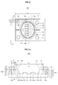
FIG. 1 is a plan view illustrating a light emitting device package according to one embodiment; -
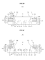
FIGs. 2A to 2C are sectional views illustrating embodiments of the light emitting device package taken along the line II-II' shown inFIG. 1 ; -
FIG. 3 is a plan view illustrating a light emitting device package according to another embodiment; -
FIGs. 4A and4B are sectional views illustrating embodiments of the light emitting device package taken along the line IV-IV' shown inFIG. 3 ; -
FIG. 5 is a sectional view illustrating a light emitting device package according to another embodiment; -
FIGs. 6A to 6D are views illustrating the method for manufacturing the light emitting device package shown inFIG. 2A ; -
FIGs. 7A to 7D are views illustrating the method for manufacturing the light emitting device package shown inFIG. 4A ; and -
FIG. 8 is a view illustrating a headlamp using the light emitting device package according to one embodiment. - Reference will now be made in detail to embodiments, examples of which are illustrated in the accompanying drawings for better understanding. However, the present disclosure may be embodied in many different forms and should not be construed as limited to the embodiments set forth herein. Rather, these embodiments are provided so that this disclosure will be thorough and complete, and will fully convey the scope of the disclosure to those skilled in the art.
-
FIG. 1 is a plan view illustrating a lightemitting device package 100A according to one embodiment. -
FIGs. 2A to 2C are sectional views of embodiments of the lightemitting device package 100A taken along the line II-II' shown inFIG. 1 . - The light
emitting device package 100A shown inFIGs. 1 to 2C includes areflective substrate 110,circuit substrates emitting diode chips 170. - The
reflective substrate 110 functions to support thecircuit substrates emitting device package 100A and includes a chip mounting region corresponding to a portion of thereflective substrate 110 defined and exposed by thecircuit substrates upper surface 110A of thereflective substrate 110 on which the lightemitting diode chip 170 is mounted. - The
reflective substrate 110 includes a material having both light reflection property and light radiation property. For example, thereflective substrate 110 has a reflectivity of 95% and is formed of a metal selected from the group consisting of aluminum (Al), silver (Ag), platinum (Pt), rhodium (Rh), radium (Rd) and palladium (Pd), or an alloy thereof, but the embodiment is not limited thereto. - In this case, when a desired level of reflectivity cannot be obtained with only the
reflective substrate 110, a reflective coating layer (not shown) to improve reflectivity of thereflective substrate 110 may be further disposed in an upper part of thereflective substrate 110. The reflective coating layer may be formed of a material which is the same as or different from a material constituting thereflective substrate 110. - In addition, when the reflective coating layer is not disposed in the upper part of the
reflective substrate 110, an anti-corrosion layer (not shown) to prevent corrosion of thereflective substrate 110 may be further disposed in the upper part of thereflective substrate 110. - In addition, when the reflective coating layer is disposed in the upper part of the
reflective substrate 110, an anti-corrosion layer (not shown) to prevent corrosion of the reflective coating layer may be disposed in the upper part of the reflective coating layer. - The anti-corrosion layer may comprise a light-transmitting resin.
- The
circuit substrates reflective substrate 110 and include first and secondinside edges holes inside edges chip mounting region 110A and the aligningholes inside edges - Here, the first and second
inside edges circuit substrates FIG. 1 . For example, the first and secondinside edges FIG. 1 . Alternatively, the first and secondinside edges FIG. 1 . - The circuit substrate may include first and
second circuit substrates chip mounting region 110A therebetween. Thefirst circuit substrate 120A has a firstinside edge 152A which defines one portion of thechip mounting region 110A and thesecond circuit substrate 120B has a secondinside edge 152B which defines another portion of thechip mounting region 110A. Each of the first andsecond circuit substrates holes - Referring to
FIGs. 2A to 2C , thecircuit substrates layer 122, awiring layer 124 andmetal layers - The
wiring layer 124 has an electrical circuit pattern and is realized with copper (Cu) or the like. - The first insulating
layer 122 is disposed between thewiring layer 124 and thereflective substrate 110 to insulate thewiring layer 124 from thereflective substrate 110. For example, the first insulatinglayer 122 may comprise an epoxy or polyamide resin, or oxide or nitride. - The metal layers 125A and 125B have a connection portion T11 which is disposed on the
wiring layer 124 to electrically connect thewires diode chip 170 to the wiring layers 125A and 125B. - For example, the
metal layers second electrode layers second electrode layers FIG. 1 , but may have a variety of shapes without limitation thereto. Thefirst electrode layer 125A is connected to thefirst electrode pad 180 and thesecond electrode layer 125B is connected to thesecond electrode pad 182. Accordingly, current may be supplied from the first andsecond electrode pads diode chip 170 via the first andsecond electrode layers wires second electrode pads second electrode layers second electrode layers diode chips 170 via thewires - The metal layers 125A and 125B may for example be formed of a metal selected from the group consisting of gold (Au), nickel (Ni), silver (Ag), copper (Cu) and palladium (Pd), or an alloy thereof, but the embodiment is not limited thereto.
- Meanwhile, the
circuit substrates adhesive layers adhesive layer 121 functions to adhere the first insulatinglayer 122 to thereflective substrate 110 and the secondadhesive layer 123 functions to adhere the first insulatinglayer 122 to thewiring layer 124. The first and secondadhesive layers adhesive layers adhesive layers - The
circuit substrates layer 126 which is disposed on themetal layers layer 126 defines the connection portion T11 of themetal layers layer 126A may be further disposed at an exposed edge of themetal layers layer 126A is illustrated in the connection portion T11, the connection portion T11 is represented with considering the solder resistlayer 126A to be omitted. - In addition, the light emitting
device package 100A may further include abarrier layer 140A. Thebarrier layer 140A may be guided by the aligningholes holes metal layers molding portion 160 described later. -
FIG. 3 is a plan view illustrating a light emittingdevice package 100B according to another embodiment. -
FIGs. 4A and4B are sectional views of embodiments of the light emittingdevice package 100B taken along the line IV-IV' shown inFIG. 3 . -
FIG. 5 is a sectional view illustrating a light emittingdevice package 100C according to another embodiment. - The barrier layers 140A and 140C of the light emitting
device packages FIGs. 1 ,2A to 2C , and5 may cover only a part of themetal layers device package 100A shown inFIGs. 1 , and2A to 2C covers only a part of themetal layers layer 126. As shown inFIG. 1 , and2A to 2C , thebarrier layer 140A may be disposed in an upper part of the solder resistlayer 126 and may be not disposed in an upper part of the connection portion T11. - Alternatively, as shown in
FIG. 5 , thebarrier layer 140C in the light emittingdevice package 100C may be disposed with being extended from the solder resistlayer 126 to the connection portion T11. - Alternatively, as shown in
FIGs. 3, 4A , and4B , thebarrier layer 140B of the light emittingdevice package 100B may cover themetal layers metal layers - Hereinafter, the same components in the light emitting device packages 100A, 100B, and 100C shown in
FIGs. 1 to 5 are represented by like reference numerals and are not described repeatedly. - As described above, in the light emitting
device packages FIGs. 1 ,2A to 2C , and5 , since the upper surface of themetal layers diode chip 170 is scattered by the exposed upper surface of themetal layers metal layers device package 100B shown inFIGs. 3, 4A and4B is completely covered with thebarrier layer 140B and is not exposed, scattering of light emitted from the light emittingdiode chip 170 is minimized and superior light extraction efficiency is thus obtained, unlike the light emittingdevice packages FIGs. 1 ,2A to 2C , and5 . - Meanwhile, a width W1 between the first and second
inside edges chip mounting region 110A in thecircuit substrates FIGs. 4A and4B , and may be different, as shown inFIGs. 2A to 2C , and5 . For example, as shown inFIGs. 2A to 2C , orFIG. 5 , the width W2 may be greater than the width W1. The width W1 between the first and secondinside edges chip mounting region 110A. - The barrier layers 140A and 140B may have a ring shape as shown in
FIGs. 1 and3 , but the embodiment is not limited thereto. In addition, the barrier layers 140A, 140B, and 140C shown inFIGs. 1 to 5 may contain a silicone or white epoxy resin, but the embodiment is not limited thereto. - Meanwhile, referring to
FIGs. 2A to 2C , the light emittingdevice package 100A may further include a second insulatinglayer 190. The secondinsulating layer 190 is disposed between the light emittingdiode chip 170 and thechip mounting region 110A of thereflective substrate 110 to isolate the light emittingdiode chip 170 from thereflective substrate 110. When the second insulatinglayer 190 is disposed, heat dissipation of the light emittingdiode chip 170 may be deteriorated. For this reason, the second insulatinglayer 190 comprises a heat dissipation material to secure heat dissipation property. Alternatively, as shown inFIGs. 4A ,4B, and 5 , the second insulatinglayer 190 may be omitted in the light emitting device packages 100B and 100C. - In this case, the second insulating
layer 190 may also function as the afore-mentioned anti-corrosion layer (not shown) to prevent corrosion of thereflective substrate 110. - The second
insulating layer 190 may contain a material which is the same as or different from that of the first insulatinglayer 122. For example, the second insulatinglayer 190 may contain an epoxy or polyamide resin, or oxide or nitride having high heat conductivity. - At least one light emitting
diode chip 170 shown inFIGs. 1 to 5 is disposed on thechip mounting region 110A of thereflective substrate 110, and is connected to the connection portions T11 of themetal layers circuit substrates wires FIGs. 1 to 5 , a plurality of the light emittingdiode chips 170 may be disposed, but the embodiment is not limited thereto. Namely, only one light emittingdiode chip 170 may be disposed. - When the light emitting
diode chip 170 includes two or more light emittingdiode chips 170, some of the light emittingdiode chips 170 may be connected to one another by at least one of parallel and series connection methods and the remaining of the light emittingdiode chips 170 may be connected to themetal layers - The afore-mentioned light emitting
diode chips 170 may be classified into horizontal- or vertical-type light emitting diode chips according to electrode position. The light emitting diode of the light emittingdiode chip 170 may include a light emitting structure including an n-type semiconductor layer, an active layer and a p-type semiconductor layer laminated in this order, and an n-type electrode and a p-type electrode which supply electrons and holes to the n-type semiconductor layer and the p-type semiconductor layer, respectively. The n-type semiconductor layer and the p-type semiconductor layer may be formed of a semiconductor compound and for example comprise a semiconductor material having a formula of InxAlyGa1-x-yN (0≤x≤1, 0≤y≤1, 0≤x+y≤1). - Regarding the light emitting
device packages FIGs. 1 and3 , twelve light emittingdiode chips 170 are connected in series between thefirst wire 150A connected to thefirst electrode layer 125A, and thesecond wire 150B connected to thesecond electrode layer 125B, but a different number of light emitting diode chips may be connected in parallel or series, but the embodiment is not limited thereto. - The portions of the
wires metal layers barrier layer 140A, as shown inFIGs. 2A to 2C , or are completely embedded in thebarrier layer 140B, as shown inFIGs. 4A and4B , or are partially embedded in thebarrier layer 140C, as shown inFIG. 5 . - Meanwhile, as shown in
FIGs. 2A ,4A , and5 , the aligningholes circuit substrates reflective substrate 110. For example, the aligninghole 102A may be spaced from the connection portion T11, as shown inFIG. 2A , or the aligninghole 102D may be disposed in the connection portion T11, as shown inFIG. 4A . Alternatively, as shown inFIG. 5 , the first and second aligningholes second circuit substrates FIG. 5 , the first aligninghole 102D is disposed in the connection portion T11 and the second aligninghole 102A is spaced from the connection portion T11. - Alternatively, as shown in
FIG. 2B , the aligninghole 102B may pass through the solder resistlayer 126 and expose only themetal layers metal layers reflective substrate 110. In addition, as shown inFIG. 2B , the aligninghole 102B exposing only themetal layers - Alternatively, as shown in
FIGs. 2C and4B , the aligningholes metal layers wiring layer 124, and the secondadhesive layer 123 of thecircuit substrates layer 122. The aligningholes 120C and 102E exposing the first insulatinglayer 122 are spaced from the connection portion T11, as shown inFIG. 2C , or are disposed in the connection portion T11, as shown inFIG. 4B , or one thereof is disposed in the connection portion T11 and another is spaced from the connection portion T11, although not shown. - Regarding the cross-sectional shape of the light emitting device package shown in
FIGs. 2A to 2C ,4A , and4B, and 5 , at least one of various shapes of aligningholes 102A to 102E may be disposed in at least one of positions provided in the connection portion T11 and positions spaced from the connection portion T11. However, at least one of the aligningholes 102A to 102C having various shapes may be disposed in at least one of positions provided in the connection portion T11 and positions spaced from the connection portion T11. - Conventionally, light and darkness of camera images are recognized based on the connection portion T11 exposed as shown in
FIGs. 2A to 2C , instead of the aligningholes 102A to 102E, and positions at which the light emittingdiode chips 170 are mounted, and positions at which thewires layer 126 are not clearly distinguished due to excessively high specular reflectivity of thereflective substrate 110, the intended arrangement is impossible. - However, in the present embodiment, as described above, one or more aligning
holes 102A to 102E are disposed in thecircuit substrates holes 102A to 102E and clear recognition between light and darkness is possible using recognition results, although specular reflectivity of thereflective substrate 110 is high during die bonding or wire bonding. For example, as shown inFIGs. 2A ,2B ,4A , and5 , when the aligningholes holes FIGs. 2C and4B , when the aligningholes holes holes 102A to 102E described above are used, the position of thechip mounting region 110A at which the light emittingdiode chips 170 are mounted, and positions at which thewires metal layers - Furthermore, as described above, the aligning holes 1 02A to 102E also function to guide positions of the embedded barrier layers 140A, 140B, and 140C.
- Furthermore, the aligning
holes 102A to 102E improve air-tightness between the barrier layers 140A, 140B, and 140C and thereflective substrate 110. - Meanwhile, the light emitting device packages 100A, 100B, and 100C may have a polygonal or round shape. For example, as shown in
FIGs. 1 and3 , the light emittingdevice packages - When the
barrier layer 140B completely covers the upper surfaces ofmetal layers FIGs. 3, 4A , and4B , the width W1 of thechip mounting region 110A may be further increased, as compared to a case in which the barrier layers 140A and 140C partially expose the upper surfaces of themetal layers FIGs. 1 ,2A to 2C , and5 . As such, when the width W1 of thechip mounting region 110A increases, more light emittingdiode chips 170 are mounted on thechip mounting region 110A in the light emitting device package having a constant size and luminous efficacy is thus improved. - For example, when the light emitting
device packages FIGs. 1 and3 , a size of the plane surface of the light emittingdevice packages - In this case, an area of the
chip mounting region 110A shown inFIGs. 1 and3 is determined by at least one of a shorter length among the lengths L1 and L2, a width T11 of the connection portion in themetal layers lateral end 101 of the light emittingdevice packages chip mounting region 110A, in which the light emittingdiode chips 170 are disposed, is determined by the distance T1 from thelateral end 101 of the light emittingdevice packages chip mounting region 110A. - For better understanding, assuming that the plane of the
chip mounting region 110A has a circular shape and L1 is the shorter among L1 and L2, the area (LEDA) of thechip mounting region 110A in the light emittingdevice packages FIGs. 1 and3 may be determined by the following Equation 1.
- In a case in which the widths T12 of the barrier layers 140A and 140B shown in
FIGs. 1 and3 are uniform, when the connection portion T11 of themetal layers barrier layer 140B and is not exposed to the outside, as shown inFIGs. 3, 4A , and4B , the distance T1 becomes shorter, as compared to a case in which the connection portion T11 of themetal layers FIGs. 1 , and2A to 2C . - In addition, when the
barrier layer 140C extends to the upper part of the connection portion T11, as exemplarily shown inFIG. 5 , the distance T1 may become shorter, than a case in which the barrier layer 140Ais not disposed in the upper part of the connection portion T11, as exemplarily shown inFIGs. 1 , and2A to 2C . - As can be seen from Equation 1, when the distance T1 becomes shorter, the area (LEDA) of the
chip mounting region 110A increases. Accordingly, the light emittingdevice package 100B shown inFIGs. 3, 4A , and4B has a large areachip mounting region 110A, as compared to the light emittingdevice package 100C shown inFIG. 5 , and the light emittingdevice package 100C shown inFIG. 5 has a large LEDA, as compared to the light emittingdevice package 100A shown inFIGs. 1 , and2A to 2C . - For this reason, luminous efficacy is improved, since the largest number of light emitting
diode chips 170 may be mounted on the light emittingdevice package 100B shown inFIG. 3, 4A , or4B , among the light emitting device packages 100A, 100B, and 100C having the same size (L1*L2). - The shortest distance T1 from the
lateral end 101 of the light emittingdevice package 100B shown inFIG. 3 to thechip mounting region 110A may be equivalent to the width T12 of thebarrier layer 140B, when the distance T13 is '0'. For example, the shortest distance T1 is 1,100 µm to 1,260 µm. - In addition, the width T12 of the barrier layers 140A and 140B may be 800 µm to 1,200 µm, and the width T11 of the connection portion in the
metal layers chip mounting region 110A may be 1:0.7 to 0.9 (L1:ϕ1). - In addition, according to the present embodiment, the distance from at least one aligning
hole 102A to 102E to the first or secondinside edges circuit substrates chip mounting region 110A. As shown inFIGs. 2A to 2C , and5 , the first reference distance may be represented by a sum of the width T11 of the connection portion, and the distance L3 from the aligninghole layer 126. For example, the first reference distance L3+T11 may be 1.176 mm. Alternatively, as shown inFIGs. 4A ,4B, and 5 , the first reference distance L4 from the aligningholes inside edges holes 102A to 102E are recognized using a camera, when the first reference distance is predetermined, the light emittingdiode chip 170 is die-bonded to an accurately recognized position of thechip mounting region 110A. - In addition, according to the present embodiment, the aligning
holes 102A to 102E may have a round plane shape or a polygonal plane shape. When the aligningholes 102A to 102C have a polygonal plane shape, a length L5 of a side of the aligningholes 102A to 102C may be 0.4 mm. Alternatively, when the aligningholes holes - In addition, when the
chip mounting region 110A is accurately recognized, the connection portion T11 contributing to wire bonding is also readily recognized. The reason for this is that the distance between the light emittingdiode chips inside edges inside edges diode chips 170 are predetermined. Accordingly, the connection portion T11 used for wire bonding is recognized from thechip mounting region 110A. - Alternatively, the connection portion T11 is recognized using the aligning
holes 102A to 102E. That is, the distance L3 from the aligningholes 102A to 102C shown inFIGs. 2A to FIG. 2C , andFIG. 5 to the end of the solder resistlayer 126 may be a second reference distance for recognizing the wire bonding region. When the solder resistlayer 126A is disposed in the connection portion T11, a part of the connection portion T11 excluding the width W3 of the solder resistlayer 126A may substantially correspond to the wire bonding region. For example, the width W3 is 100 µm and the distance L3 is 1.28 mm. Alternatively, as shown inFIGs. 4A ,4B, and 5 , the second reference distance is a distance from the aligningholes inside edges holes layer 126, which corresponds to the connection portion T11 used for wire bonding. When the solder resistlayer 126A is disposed, a part of the connection portion T11 excluding the width W3 substantially corresponds to the wire bonding region. - The light emitting device packages 100A, 100B, and 100C shown in
FIGs. 1 to 5 have a configuration in which the light emitting device packages 100A, 100B, and 100C is not filled with themolding portion 160 so as to illustrate connection between the light emitting diode chips 170. However, as described below, the light emitting device packages 100A, 100B, and 100C further include themolding portion 160. Themolding portion 160 seals at least one light emittingdiode chip 170 and thewires chip mounting region 110A. - Meanwhile, the afore-mentioned light emitting device packages 100A, 100B, and 100C include a protection device such as Zener diode (not shown) connected to the light emitting
diode chips 170 in a reverse direction to effectively block electrostatic discharge (ESD) voltage applied from the outside and thereby protect the light emittingdiode chip 170. - Hereinafter, a method for manufacturing the light emitting
device packages -
FIGs. 6A to 6D are views illustrating the method for manufacturing the light emittingdevice package 100A shown inFIG. 2A . -
FIG. 6B is a sectional view taken along the line Vlb-Vlb' shown inFIG. 6A , andFIG. 6D is a sectional view taken along the line Vld-Vld' shown inFIG. 6C . - Referring to
FIGs. 6A and 6B ,circuit substrates chip mounting region 110A having a round plane shape are formed on thereflective substrate 110. That is, a firstadhesive layer 121, a first insulatinglayer 122, a secondadhesive layer 123 and awiring layer 124 are formed on thereflective substrate 110,metal layers wiring layer 124, and a solder resistlayer 126 is formed on themetal layers - At this time, an aligning
hole 102A is formed at a position spaced from the connection portion T11. As described above, as shown inFIG. 6A , the aligninghole 102A may have a rectangular plane shape. Then, thechip mounting region 110A is recognized, based on the aligninghole 102A and a plurality of light emittingdiode chips 170 are formed in the recognizedchip mounting region 110A. Then, a connection portion T11 serving as a wire bonding region is recognized and the recognized connection portion T11 is connected to the light emittingdiode chip 170 through thewires hole 102A may be used to recognize the connection portion T11, as described above. - Then, as shown in
FIGs. 1 and 2A , abarrier layer 140A is formed on the upper surface of the solder resistlayer 126 such that the connection portion T11 which is a part of an upper surface of themetal layers - Then, as shown in
FIGs. 6C and 6D , thechip mounting region 110A is filled with themolding portion 160 sealing at least one light emittingdiode chip 170 and thewires device package 100A. -
FIGs. 7A to 7D are views illustrating the method for manufacturing the light emittingdevice package 100B shown inFIG. 4A . -
FIG. 7B is a sectional view taken along the line Vllb-Vllb' shown inFIG. 7A andFIG. 7D is a sectional view taken along the line Vlld-Vlld' shown inFIG. 7C . - Referring to
FIGs. 7A and 7B ,circuit substrates chip mounting region 110A having a round plane shape are formed on thereflective substrate 110. That is, a firstadhesive layer 121, a first insulatinglayer 122, a secondadhesive layer 123 and awiring layer 124 are formed on thereflective substrate 110,metal layers wiring layer 124, and a solder resistlayer 126 is formed on themetal layers - At this time, an aligning
hole 102D is formed in the connection portion T11. As described above, as shown inFIG. 7A , the aligninghole 102D may have a circular plane shape. Then, thechip mounting region 110A is recognized, based on the aligninghole 102A and a plurality of light emittingdiode chips 170 are formed in the recognizedchip mounting region 110A. Then, a connection portion T11 serving as a wire bonding region is recognized and the recognized connection portion T11 is connected to the light emittingdiode chip 170 through thewires hole 102D. - Next, as shown in
FIGs. 3 and 4A , abarrier layer 140B is formed on the upper surface of the solder resistlayer 126, and themetal layers metal layers - Next, as shown in
FIGs. 7C and 7D , thechip mounting region 110A is filled with themolding portion 160 sealing at least one light emittingdiode chip 170 and thewires device package 100A. - The
molding portion 160 is for example formed of a solid transparent resin, a silicone resin, an epoxy resin or a mixture thereof. The upper surface of themolding portion 160 may be round or flat and a lens or dome resin material (not shown) may be further disposed on the upper surface of themolding portion 160, although not shown. - A height of the
molding portion 160 may be lower than that of thebarrier layer 140A, as shown inFIG. 6D , or may be equivalent to that of thebarrier layer 140B, as shown inFIG. 7D . - In addition, the
molding portion 160 may further include aphosphor 162 so as to change wavelength of light emitted from the light emittingdiode chip 170. - The
phosphor 162 may include a garnet-based phosphor, a silicate-based phosphor, a nitride-based phosphor or an oxynitride-based phosphor. - For example, the garnet-based phosphor may be YAG(Y3Al5O12:Ce3+) or TAG (Tb3Al5O12:Ce3+), the silicate-based phosphor may be (Sr,Ba,Mg,Ca)2SiO4:Eu2+, the nitride-based phosphor may be CaAlSiN3:Eu2+ containing SiN, and the oxynitride-based phosphor may be Si6-xAlxOxN8-x:Eu2+ (0<x<6) containing SiON.
- Meanwhile, the light emitting
diode chips 170 are mounted in the light emitting device packages 100A, 100B, and 100C in a chip on board (COB) form, and may be integrated in an array or module form in one package, without limitation thereto. - In the light emitting device package according to the present embodiment, at least one aligning hole is disposed in the circuit substrate, light and darkness of camera images are recognized based on the aligning hole, and clear recognition of light and darkness is possible using the recognized results although specular reflectivity of the reflective substrate is high during die bonding or wire bonding. Therefore, the light emitting diode chips and the wires are aligned at accurate positions, guiding of the position of the embedded barrier layer is possible, and air-tightness between the barrier layer and the reflective substrate is improved.
-
FIG. 8 is a view illustrating a headlamp using the light emitting device package according to one embodiment. - Referring to
FIG. 8 , light passing through a glass cover of the light emittingdevice package 801 is reflected by areflector 802 and ashade 803, passes through alens 804, and travels toward the front of a car body having the headlamp. The light emittingdevice package 801 corresponds to the light emitting device packages 100A, 100B, and 100C, shown inFIGs. 1 to 7D . - In addition, a plurality of light emitting device packages including the light emitting device package related to this embodiment are arrayed on a substrate, and optical members such as light guide plates, prism sheets, diffusion sheets or the like may be arranged in the light passage of the light emitting device packages. The light emitting device package, substrate and optical members may serve as light units. Another embodiment is realized with a display device, an indicator device or a lighting system including the semiconductor light emitting device or the light emitting device package mentioned in the previous embodiments, and examples of the lighting system may include lamps, street lights and the like.
- Although embodiments have been described with reference to a number of illustrative embodiments thereof, it should be understood that numerous other modifications and embodiments can be devised by those skilled in the art that will fall within the spirit and scope of the principles of this disclosure. More particularly, various variations and modifications are possible in the component parts and/or arrangements of the subject combination arrangement within the scope of the disclosure, the drawings and the appended claims. In addition to variations and modifications in the component parts and/or arrangements, alternative uses will also be apparent to those skilled in the art.
Claims (15)
- A light emitting device package, comprising:a reflective substrate including a chip mounting region;a circuit substrate disposed on the reflective substrate, the circuit substrate including an inside edge defining the chip mounting region and at least one aligning hole disposed at a position spaced from the inside edge; andat least one light emitting diode chip disposed in the chip mounting region, the at least one light emitting diode chip being connected to the circuit substrate through a wire.
- The light emitting device package according to claim 1, wherein the circuit substrate comprises a first circuit substrate and a second circuit substrate facing each other with interposing the chip mounting region therebetween,
the first circuit substrate has a first inside edge defining one part of the chip mounting region,
the second circuit substrate has a second inside edge defining another part of the chip mounting region, and
each of the first and second circuit substrates has the at least one aligning hole. - The light emitting device package according to claim 1 or 2, wherein the circuit substrate comprises:a wiring layer;a first insulating layer disposed between the wiring layer and the reflective substrate; anda metal layer having a connection portion disposed on the wiring layer, the connection portion electrically connecting the wire connected to the light emitting diode chip to the wiring layer.
- The light emitting device package according to any one of claims 1 to 3, further comprising a second insulating layer disposed between the light emitting diode chip and the reflective substrate.
- The light emitting device package according to claim 3, wherein the circuit substrate further comprises a solder resist layer disposed on the metal layer such that the solder resist layer does not overlap the connection portion.
- The light emitting device package according to claim 5, wherein the at least one aligning hole passes through the solder resist layer and exposes the metal layer.
- The light emitting device package according to any one of claims 1 to 5, wherein the at least one aligning hole passes through the circuit substrate and exposes the reflective substrate.
- The light emitting device package according to any one of claims 3 to 5, wherein the at least one aligning hole passes through the metal layer and the wiring layer, and exposes the first insulating layer.
- The light emitting device package according to any one of claims 3 to 8, wherein the at least one aligning hole is disposed in the connection portion.
- The light emitting device package according to any one of claims 3 to 8, wherein the at least one aligning hole is disposed at a position spaced from the connection portion.
- The light emitting device package according to any one of claims 3 to 10, wherein the at least one aligning hole comprises:a first aligning hole disposed in the connection portion; anda second aligning hole at a position spaced from the connection portion.
- The light emitting device package according to any one of claims 6, 9 and 11, further comprising a barrier layer disposed on the circuit substrate such that the barrier layer embeds the at least one aligning hole.
- The light emitting device package according to claim 12, wherein the barrier layer is disposed on the connection portion.
- The light emitting device package according to claim 12, wherein the barrier layer extends from the solder resist layer to the connection portion.
- The light emitting device package according to any one of claims 1 to 14, further comprising a molding portion sealing the at least one light emitting diode chip and the wire on the chip mounting region.
Applications Claiming Priority (1)
| Application Number | Priority Date | Filing Date | Title |
|---|---|---|---|
| KR1020120073696A KR101922528B1 (en) | 2012-07-06 | 2012-07-06 | Light emitting device package |
Publications (3)
| Publication Number | Publication Date |
|---|---|
| EP2682987A2 true EP2682987A2 (en) | 2014-01-08 |
| EP2682987A3 EP2682987A3 (en) | 2015-11-18 |
| EP2682987B1 EP2682987B1 (en) | 2018-04-04 |
Family
ID=48446170
Family Applications (1)
| Application Number | Title | Priority Date | Filing Date |
|---|---|---|---|
| EP13168598.4A Active EP2682987B1 (en) | 2012-07-06 | 2013-05-21 | Light emitting device package |
Country Status (4)
| Country | Link |
|---|---|
| US (1) | US9057501B2 (en) |
| EP (1) | EP2682987B1 (en) |
| KR (1) | KR101922528B1 (en) |
| CN (1) | CN103531584B (en) |
Families Citing this family (15)
| Publication number | Priority date | Publication date | Assignee | Title |
|---|---|---|---|---|
| JP1524801S (en) * | 2014-05-26 | 2015-06-01 | ||
| USD771579S1 (en) * | 2014-05-26 | 2016-11-15 | Citizens Electronics Co., Ltd. | Light emitting diode |
| USD767515S1 (en) * | 2014-10-24 | 2016-09-27 | Citizen Electronics Co., Ltd. | Light emitting diode |
| JP1545462S (en) * | 2015-05-20 | 2016-03-14 | ||
| USD786809S1 (en) | 2015-05-20 | 2017-05-16 | Citizen Electronics Co., Ltd. | Light emitting diode |
| KR102466959B1 (en) | 2015-12-31 | 2022-11-11 | 엘지디스플레이 주식회사 | Organic Light Emitting Display Device |
| CN105870113A (en) * | 2016-05-26 | 2016-08-17 | 郑州中瓷科技有限公司 | LED light source structure and preparation method thereof |
| TWI616616B (en) * | 2017-03-20 | 2018-03-01 | 蔡高德 | LED plane light source lamp |
| JP7177327B2 (en) * | 2017-04-06 | 2022-11-24 | 日亜化学工業株式会社 | light emitting device |
| WO2019012793A1 (en) * | 2017-07-13 | 2019-01-17 | ソニー株式会社 | Light emitting device, display device, and illuminating device |
| TWI684293B (en) * | 2018-06-29 | 2020-02-01 | 同泰電子科技股份有限公司 | Backlight circuit board structure with high reflectivity and method for making thereof |
| JP6729672B2 (en) * | 2018-12-14 | 2020-07-22 | 日亜化学工業株式会社 | Light emitting device |
| CN114258192B (en) * | 2020-09-23 | 2024-10-15 | 庆鼎精密电子(淮安)有限公司 | Circuit board with high reflectivity and manufacturing method thereof |
| JP7104348B2 (en) * | 2020-10-28 | 2022-07-21 | 日亜化学工業株式会社 | Luminescent device |
| CN114678350A (en) * | 2022-01-18 | 2022-06-28 | 深圳市创显光电有限公司 | A composite display screen with cob light source installed |
Family Cites Families (9)
| Publication number | Priority date | Publication date | Assignee | Title |
|---|---|---|---|---|
| JP3956965B2 (en) * | 2004-09-07 | 2007-08-08 | 日立エーアイシー株式会社 | Chip component type light emitting device and wiring board therefor |
| JP5089212B2 (en) * | 2007-03-23 | 2012-12-05 | シャープ株式会社 | LIGHT EMITTING DEVICE, LED LAMP USING THE SAME, AND METHOD FOR MANUFACTURING LIGHT EMITTING DEVICE |
| TW200843135A (en) * | 2007-04-23 | 2008-11-01 | Augux Co Ltd | Method of packaging light emitting diode with high heat-dissipating efficiency and the structure thereof |
| TW200845877A (en) * | 2007-05-07 | 2008-11-16 | Tysun Inc | Heat-dissipating substrates of composite structure |
| CN101539254B (en) * | 2009-05-08 | 2010-07-21 | 罗本杰 | Reflective and radiating base of high-power LED light source |
| CN201827671U (en) * | 2009-05-08 | 2011-05-11 | 罗本杰(北京)光电研究所有限公司 | Reflective and heat radiation base for high-power LED light source |
| CN101761894A (en) * | 2009-12-29 | 2010-06-30 | 罗本杰 | Reflecting heat radiation and sealing base of high-power LED light source |
| CN201655836U (en) * | 2009-12-29 | 2010-11-24 | 罗本杰(北京)光电研究所有限公司 | Reflecting, radiating and sealing base of high power LED light source |
| DE102010026344A1 (en) * | 2010-07-07 | 2012-01-12 | Osram Opto Semiconductors Gmbh | led |
-
2012
- 2012-07-06 KR KR1020120073696A patent/KR101922528B1/en not_active Expired - Fee Related
-
2013
- 2013-04-23 US US13/868,812 patent/US9057501B2/en active Active
- 2013-05-21 EP EP13168598.4A patent/EP2682987B1/en active Active
- 2013-06-03 CN CN201310216888.8A patent/CN103531584B/en active Active
Non-Patent Citations (1)
| Title |
|---|
| None |
Also Published As
| Publication number | Publication date |
|---|---|
| KR20140006526A (en) | 2014-01-16 |
| EP2682987A3 (en) | 2015-11-18 |
| US20140009941A1 (en) | 2014-01-09 |
| US9057501B2 (en) | 2015-06-16 |
| CN103531584B (en) | 2017-10-03 |
| KR101922528B1 (en) | 2018-11-28 |
| CN103531584A (en) | 2014-01-22 |
| EP2682987B1 (en) | 2018-04-04 |
Similar Documents
| Publication | Publication Date | Title |
|---|---|---|
| EP2682987B1 (en) | Light emitting device package | |
| US10950759B2 (en) | LED module | |
| US10217918B2 (en) | Light-emitting element package | |
| EP3309835B1 (en) | Light emitting device package | |
| US9231166B2 (en) | Light emitting device and lighting apparatus having the same | |
| US8916887B2 (en) | Light emitting device package and lighting system using the same | |
| US8519427B2 (en) | Light emitting device and lighting system | |
| US9564564B2 (en) | Light emitting device and lighting apparatus having the same | |
| US9620693B2 (en) | Light emitting device and lighting system having the same | |
| US9249957B2 (en) | Light emitting device and lighting system including the same | |
| CN102479910A (en) | Led module | |
| KR20140020789A (en) | Light emitting device | |
| US9490184B2 (en) | Light emitting device and manufacturing method thereof | |
| KR20140095723A (en) | Light emitting device and light apparatus having thereof | |
| KR102520094B1 (en) | A light emitting device package | |
| KR101911866B1 (en) | Light emitting device package | |
| KR102142718B1 (en) | Light emitting device and light apparatus having thereof | |
| KR20150137784A (en) | A light emitting device package | |
| KR20160024523A (en) | A light emitting device package |
Legal Events
| Date | Code | Title | Description |
|---|---|---|---|
| PUAI | Public reference made under article 153(3) epc to a published international application that has entered the european phase |
Free format text: ORIGINAL CODE: 0009012 |
|
| AK | Designated contracting states |
Kind code of ref document: A2 Designated state(s): AL AT BE BG CH CY CZ DE DK EE ES FI FR GB GR HR HU IE IS IT LI LT LU LV MC MK MT NL NO PL PT RO RS SE SI SK SM TR |
|
| AX | Request for extension of the european patent |
Extension state: BA ME |
|
| 17P | Request for examination filed |
Effective date: 20140328 |
|
| RBV | Designated contracting states (corrected) |
Designated state(s): AL AT BE BG CH CY CZ DE DK EE ES FI FR GB GR HR HU IE IS IT LI LT LU LV MC MK MT NL NO PL PT RO RS SE SI SK SM TR |
|
| RAP1 | Party data changed (applicant data changed or rights of an application transferred) |
Owner name: LG INNOTEK CO., LTD. |
|
| PUAL | Search report despatched |
Free format text: ORIGINAL CODE: 0009013 |
|
| AK | Designated contracting states |
Kind code of ref document: A3 Designated state(s): AL AT BE BG CH CY CZ DE DK EE ES FI FR GB GR HR HU IE IS IT LI LT LU LV MC MK MT NL NO PL PT RO RS SE SI SK SM TR |
|
| AX | Request for extension of the european patent |
Extension state: BA ME |
|
| RIC1 | Information provided on ipc code assigned before grant |
Ipc: H01L 23/00 20060101ALN20151012BHEP Ipc: H01L 25/075 20060101AFI20151012BHEP Ipc: H01L 33/62 20100101ALI20151012BHEP Ipc: H01L 23/544 20060101ALI20151012BHEP Ipc: H01L 33/60 20100101ALN20151012BHEP |
|
| RAP1 | Party data changed (applicant data changed or rights of an application transferred) |
Owner name: LG INNOTEK CO., LTD. |
|
| GRAP | Despatch of communication of intention to grant a patent |
Free format text: ORIGINAL CODE: EPIDOSNIGR1 |
|
| STAA | Information on the status of an ep patent application or granted ep patent |
Free format text: STATUS: GRANT OF PATENT IS INTENDED |
|
| RIC1 | Information provided on ipc code assigned before grant |
Ipc: H01L 33/62 20100101ALI20170914BHEP Ipc: H01L 23/544 20060101ALI20170914BHEP Ipc: H01L 33/60 20100101ALN20170914BHEP Ipc: H01L 23/00 20060101ALN20170914BHEP Ipc: H01L 25/075 20060101AFI20170914BHEP |
|
| RIC1 | Information provided on ipc code assigned before grant |
Ipc: H01L 33/60 20100101ALN20170921BHEP Ipc: H01L 23/00 20060101ALN20170921BHEP Ipc: H01L 23/544 20060101ALI20170921BHEP Ipc: H01L 33/62 20100101ALI20170921BHEP Ipc: H01L 25/075 20060101AFI20170921BHEP |
|
| INTG | Intention to grant announced |
Effective date: 20171009 |
|
| RIN1 | Information on inventor provided before grant (corrected) |
Inventor name: CHO, HYUN SEOK |
|
| GRAS | Grant fee paid |
Free format text: ORIGINAL CODE: EPIDOSNIGR3 |
|
| GRAA | (expected) grant |
Free format text: ORIGINAL CODE: 0009210 |
|
| STAA | Information on the status of an ep patent application or granted ep patent |
Free format text: STATUS: THE PATENT HAS BEEN GRANTED |
|
| AK | Designated contracting states |
Kind code of ref document: B1 Designated state(s): AL AT BE BG CH CY CZ DE DK EE ES FI FR GB GR HR HU IE IS IT LI LT LU LV MC MK MT NL NO PL PT RO RS SE SI SK SM TR |
|
| REG | Reference to a national code |
Ref country code: GB Ref legal event code: FG4D |
|
| REG | Reference to a national code |
Ref country code: CH Ref legal event code: EP |
|
| REG | Reference to a national code |
Ref country code: AT Ref legal event code: REF Ref document number: 986467 Country of ref document: AT Kind code of ref document: T Effective date: 20180415 |
|
| REG | Reference to a national code |
Ref country code: IE Ref legal event code: FG4D |
|
| REG | Reference to a national code |
Ref country code: DE Ref legal event code: R096 Ref document number: 602013035297 Country of ref document: DE |
|
| REG | Reference to a national code |
Ref country code: NL Ref legal event code: MP Effective date: 20180404 |
|
| REG | Reference to a national code |
Ref country code: LT Ref legal event code: MG4D |
|
| PG25 | Lapsed in a contracting state [announced via postgrant information from national office to epo] |
Ref country code: NL Free format text: LAPSE BECAUSE OF FAILURE TO SUBMIT A TRANSLATION OF THE DESCRIPTION OR TO PAY THE FEE WITHIN THE PRESCRIBED TIME-LIMIT Effective date: 20180404 |
|
| PG25 | Lapsed in a contracting state [announced via postgrant information from national office to epo] |
Ref country code: ES Free format text: LAPSE BECAUSE OF FAILURE TO SUBMIT A TRANSLATION OF THE DESCRIPTION OR TO PAY THE FEE WITHIN THE PRESCRIBED TIME-LIMIT Effective date: 20180404 Ref country code: AL Free format text: LAPSE BECAUSE OF FAILURE TO SUBMIT A TRANSLATION OF THE DESCRIPTION OR TO PAY THE FEE WITHIN THE PRESCRIBED TIME-LIMIT Effective date: 20180404 Ref country code: SE Free format text: LAPSE BECAUSE OF FAILURE TO SUBMIT A TRANSLATION OF THE DESCRIPTION OR TO PAY THE FEE WITHIN THE PRESCRIBED TIME-LIMIT Effective date: 20180404 Ref country code: LT Free format text: LAPSE BECAUSE OF FAILURE TO SUBMIT A TRANSLATION OF THE DESCRIPTION OR TO PAY THE FEE WITHIN THE PRESCRIBED TIME-LIMIT Effective date: 20180404 Ref country code: PL Free format text: LAPSE BECAUSE OF FAILURE TO SUBMIT A TRANSLATION OF THE DESCRIPTION OR TO PAY THE FEE WITHIN THE PRESCRIBED TIME-LIMIT Effective date: 20180404 Ref country code: NO Free format text: LAPSE BECAUSE OF FAILURE TO SUBMIT A TRANSLATION OF THE DESCRIPTION OR TO PAY THE FEE WITHIN THE PRESCRIBED TIME-LIMIT Effective date: 20180704 Ref country code: FI Free format text: LAPSE BECAUSE OF FAILURE TO SUBMIT A TRANSLATION OF THE DESCRIPTION OR TO PAY THE FEE WITHIN THE PRESCRIBED TIME-LIMIT Effective date: 20180404 Ref country code: BG Free format text: LAPSE BECAUSE OF FAILURE TO SUBMIT A TRANSLATION OF THE DESCRIPTION OR TO PAY THE FEE WITHIN THE PRESCRIBED TIME-LIMIT Effective date: 20180704 |
|
| PG25 | Lapsed in a contracting state [announced via postgrant information from national office to epo] |
Ref country code: RS Free format text: LAPSE BECAUSE OF FAILURE TO SUBMIT A TRANSLATION OF THE DESCRIPTION OR TO PAY THE FEE WITHIN THE PRESCRIBED TIME-LIMIT Effective date: 20180404 Ref country code: LV Free format text: LAPSE BECAUSE OF FAILURE TO SUBMIT A TRANSLATION OF THE DESCRIPTION OR TO PAY THE FEE WITHIN THE PRESCRIBED TIME-LIMIT Effective date: 20180404 Ref country code: GR Free format text: LAPSE BECAUSE OF FAILURE TO SUBMIT A TRANSLATION OF THE DESCRIPTION OR TO PAY THE FEE WITHIN THE PRESCRIBED TIME-LIMIT Effective date: 20180705 Ref country code: HR Free format text: LAPSE BECAUSE OF FAILURE TO SUBMIT A TRANSLATION OF THE DESCRIPTION OR TO PAY THE FEE WITHIN THE PRESCRIBED TIME-LIMIT Effective date: 20180404 |
|
| REG | Reference to a national code |
Ref country code: CH Ref legal event code: PL |
|
| REG | Reference to a national code |
Ref country code: AT Ref legal event code: MK05 Ref document number: 986467 Country of ref document: AT Kind code of ref document: T Effective date: 20180404 |
|
| PG25 | Lapsed in a contracting state [announced via postgrant information from national office to epo] |
Ref country code: PT Free format text: LAPSE BECAUSE OF FAILURE TO SUBMIT A TRANSLATION OF THE DESCRIPTION OR TO PAY THE FEE WITHIN THE PRESCRIBED TIME-LIMIT Effective date: 20180806 |
|
| REG | Reference to a national code |
Ref country code: DE Ref legal event code: R097 Ref document number: 602013035297 Country of ref document: DE |
|
| REG | Reference to a national code |
Ref country code: BE Ref legal event code: MM Effective date: 20180531 |
|
| PG25 | Lapsed in a contracting state [announced via postgrant information from national office to epo] |
Ref country code: SK Free format text: LAPSE BECAUSE OF FAILURE TO SUBMIT A TRANSLATION OF THE DESCRIPTION OR TO PAY THE FEE WITHIN THE PRESCRIBED TIME-LIMIT Effective date: 20180404 Ref country code: MC Free format text: LAPSE BECAUSE OF FAILURE TO SUBMIT A TRANSLATION OF THE DESCRIPTION OR TO PAY THE FEE WITHIN THE PRESCRIBED TIME-LIMIT Effective date: 20180404 Ref country code: DK Free format text: LAPSE BECAUSE OF FAILURE TO SUBMIT A TRANSLATION OF THE DESCRIPTION OR TO PAY THE FEE WITHIN THE PRESCRIBED TIME-LIMIT Effective date: 20180404 Ref country code: AT Free format text: LAPSE BECAUSE OF FAILURE TO SUBMIT A TRANSLATION OF THE DESCRIPTION OR TO PAY THE FEE WITHIN THE PRESCRIBED TIME-LIMIT Effective date: 20180404 Ref country code: EE Free format text: LAPSE BECAUSE OF FAILURE TO SUBMIT A TRANSLATION OF THE DESCRIPTION OR TO PAY THE FEE WITHIN THE PRESCRIBED TIME-LIMIT Effective date: 20180404 Ref country code: RO Free format text: LAPSE BECAUSE OF FAILURE TO SUBMIT A TRANSLATION OF THE DESCRIPTION OR TO PAY THE FEE WITHIN THE PRESCRIBED TIME-LIMIT Effective date: 20180404 Ref country code: CZ Free format text: LAPSE BECAUSE OF FAILURE TO SUBMIT A TRANSLATION OF THE DESCRIPTION OR TO PAY THE FEE WITHIN THE PRESCRIBED TIME-LIMIT Effective date: 20180404 |
|
| PLBE | No opposition filed within time limit |
Free format text: ORIGINAL CODE: 0009261 |
|
| STAA | Information on the status of an ep patent application or granted ep patent |
Free format text: STATUS: NO OPPOSITION FILED WITHIN TIME LIMIT |
|
| REG | Reference to a national code |
Ref country code: IE Ref legal event code: MM4A |
|
| PG25 | Lapsed in a contracting state [announced via postgrant information from national office to epo] |
Ref country code: IT Free format text: LAPSE BECAUSE OF FAILURE TO SUBMIT A TRANSLATION OF THE DESCRIPTION OR TO PAY THE FEE WITHIN THE PRESCRIBED TIME-LIMIT Effective date: 20180404 Ref country code: LI Free format text: LAPSE BECAUSE OF NON-PAYMENT OF DUE FEES Effective date: 20180531 Ref country code: CH Free format text: LAPSE BECAUSE OF NON-PAYMENT OF DUE FEES Effective date: 20180531 Ref country code: SM Free format text: LAPSE BECAUSE OF FAILURE TO SUBMIT A TRANSLATION OF THE DESCRIPTION OR TO PAY THE FEE WITHIN THE PRESCRIBED TIME-LIMIT Effective date: 20180404 |
|
| 26N | No opposition filed |
Effective date: 20190107 |
|
| GBPC | Gb: european patent ceased through non-payment of renewal fee |
Effective date: 20180704 |
|
| PG25 | Lapsed in a contracting state [announced via postgrant information from national office to epo] |
Ref country code: LU Free format text: LAPSE BECAUSE OF NON-PAYMENT OF DUE FEES Effective date: 20180521 |
|
| PG25 | Lapsed in a contracting state [announced via postgrant information from national office to epo] |
Ref country code: IE Free format text: LAPSE BECAUSE OF NON-PAYMENT OF DUE FEES Effective date: 20180521 Ref country code: GB Free format text: LAPSE BECAUSE OF NON-PAYMENT OF DUE FEES Effective date: 20180704 Ref country code: FR Free format text: LAPSE BECAUSE OF NON-PAYMENT OF DUE FEES Effective date: 20180604 |
|
| PG25 | Lapsed in a contracting state [announced via postgrant information from national office to epo] |
Ref country code: BE Free format text: LAPSE BECAUSE OF NON-PAYMENT OF DUE FEES Effective date: 20180531 Ref country code: SI Free format text: LAPSE BECAUSE OF FAILURE TO SUBMIT A TRANSLATION OF THE DESCRIPTION OR TO PAY THE FEE WITHIN THE PRESCRIBED TIME-LIMIT Effective date: 20180404 |
|
| PG25 | Lapsed in a contracting state [announced via postgrant information from national office to epo] |
Ref country code: MT Free format text: LAPSE BECAUSE OF NON-PAYMENT OF DUE FEES Effective date: 20180521 |
|
| PG25 | Lapsed in a contracting state [announced via postgrant information from national office to epo] |
Ref country code: TR Free format text: LAPSE BECAUSE OF FAILURE TO SUBMIT A TRANSLATION OF THE DESCRIPTION OR TO PAY THE FEE WITHIN THE PRESCRIBED TIME-LIMIT Effective date: 20180404 |
|
| PG25 | Lapsed in a contracting state [announced via postgrant information from national office to epo] |
Ref country code: HU Free format text: LAPSE BECAUSE OF FAILURE TO SUBMIT A TRANSLATION OF THE DESCRIPTION OR TO PAY THE FEE WITHIN THE PRESCRIBED TIME-LIMIT; INVALID AB INITIO Effective date: 20130521 |
|
| PG25 | Lapsed in a contracting state [announced via postgrant information from national office to epo] |
Ref country code: CY Free format text: LAPSE BECAUSE OF FAILURE TO SUBMIT A TRANSLATION OF THE DESCRIPTION OR TO PAY THE FEE WITHIN THE PRESCRIBED TIME-LIMIT Effective date: 20180404 Ref country code: MK Free format text: LAPSE BECAUSE OF NON-PAYMENT OF DUE FEES Effective date: 20180404 |
|
| PG25 | Lapsed in a contracting state [announced via postgrant information from national office to epo] |
Ref country code: IS Free format text: LAPSE BECAUSE OF FAILURE TO SUBMIT A TRANSLATION OF THE DESCRIPTION OR TO PAY THE FEE WITHIN THE PRESCRIBED TIME-LIMIT Effective date: 20180804 |
|
| REG | Reference to a national code |
Ref country code: DE Ref legal event code: R081 Ref document number: 602013035297 Country of ref document: DE Owner name: SUZHOU LEKIN SEMICONDUCTOR CO. LTD., TAICANG, CN Free format text: FORMER OWNER: LG INNOTEK CO., LTD., SEOUL, KR |
|
| REG | Reference to a national code |
Ref country code: DE Ref legal event code: R079 Ref document number: 602013035297 Country of ref document: DE Free format text: PREVIOUS MAIN CLASS: H01L0025075000 Ipc: H10H0029240000 |
|
| PGFP | Annual fee paid to national office [announced via postgrant information from national office to epo] |
Ref country code: DE Payment date: 20250408 Year of fee payment: 13 |