EP2680306A1 - Power transistor with heat dissipation and method therefore - Google Patents
Power transistor with heat dissipation and method therefore Download PDFInfo
- Publication number
- EP2680306A1 EP2680306A1 EP13172879.2A EP13172879A EP2680306A1 EP 2680306 A1 EP2680306 A1 EP 2680306A1 EP 13172879 A EP13172879 A EP 13172879A EP 2680306 A1 EP2680306 A1 EP 2680306A1
- Authority
- EP
- European Patent Office
- Prior art keywords
- die
- legs
- power
- attaching
- attached
- Prior art date
- Legal status (The legal status is an assumption and is not a legal conclusion. Google has not performed a legal analysis and makes no representation as to the accuracy of the status listed.)
- Granted
Links
Images
Classifications
-
- H—ELECTRICITY
- H10—SEMICONDUCTOR DEVICES; ELECTRIC SOLID-STATE DEVICES NOT OTHERWISE PROVIDED FOR
- H10W—GENERIC PACKAGES, INTERCONNECTIONS, CONNECTORS OR OTHER CONSTRUCTIONAL DETAILS OF DEVICES COVERED BY CLASS H10
- H10W40/00—Arrangements for thermal protection or thermal control
- H10W40/10—Arrangements for heating
-
- H—ELECTRICITY
- H10—SEMICONDUCTOR DEVICES; ELECTRIC SOLID-STATE DEVICES NOT OTHERWISE PROVIDED FOR
- H10W—GENERIC PACKAGES, INTERCONNECTIONS, CONNECTORS OR OTHER CONSTRUCTIONAL DETAILS OF DEVICES COVERED BY CLASS H10
- H10W40/00—Arrangements for thermal protection or thermal control
- H10W40/20—Arrangements for cooling
- H10W40/22—Arrangements for cooling characterised by their shape, e.g. having conical or cylindrical projections
-
- H—ELECTRICITY
- H10—SEMICONDUCTOR DEVICES; ELECTRIC SOLID-STATE DEVICES NOT OTHERWISE PROVIDED FOR
- H10W—GENERIC PACKAGES, INTERCONNECTIONS, CONNECTORS OR OTHER CONSTRUCTIONAL DETAILS OF DEVICES COVERED BY CLASS H10
- H10W40/00—Arrangements for thermal protection or thermal control
- H10W40/70—Fillings or auxiliary members in containers or in encapsulations for thermal protection or control
-
- H—ELECTRICITY
- H10—SEMICONDUCTOR DEVICES; ELECTRIC SOLID-STATE DEVICES NOT OTHERWISE PROVIDED FOR
- H10W—GENERIC PACKAGES, INTERCONNECTIONS, CONNECTORS OR OTHER CONSTRUCTIONAL DETAILS OF DEVICES COVERED BY CLASS H10
- H10W40/00—Arrangements for thermal protection or thermal control
- H10W40/70—Fillings or auxiliary members in containers or in encapsulations for thermal protection or control
- H10W40/77—Auxiliary members characterised by their shape
- H10W40/778—Auxiliary members characterised by their shape in encapsulations
-
- H—ELECTRICITY
- H10—SEMICONDUCTOR DEVICES; ELECTRIC SOLID-STATE DEVICES NOT OTHERWISE PROVIDED FOR
- H10W—GENERIC PACKAGES, INTERCONNECTIONS, CONNECTORS OR OTHER CONSTRUCTIONAL DETAILS OF DEVICES COVERED BY CLASS H10
- H10W70/00—Package substrates; Interposers; Redistribution layers [RDL]
- H10W70/40—Leadframes
- H10W70/481—Leadframes for devices being provided for in groups H10D8/00 - H10D48/00
-
- H—ELECTRICITY
- H10—SEMICONDUCTOR DEVICES; ELECTRIC SOLID-STATE DEVICES NOT OTHERWISE PROVIDED FOR
- H10W—GENERIC PACKAGES, INTERCONNECTIONS, CONNECTORS OR OTHER CONSTRUCTIONAL DETAILS OF DEVICES COVERED BY CLASS H10
- H10W90/00—Package configurations
- H10W90/701—Package configurations characterised by the relative positions of pads or connectors relative to package parts
- H10W90/751—Package configurations characterised by the relative positions of pads or connectors relative to package parts of bond wires
- H10W90/753—Package configurations characterised by the relative positions of pads or connectors relative to package parts of bond wires between laterally-adjacent chips
-
- H—ELECTRICITY
- H10—SEMICONDUCTOR DEVICES; ELECTRIC SOLID-STATE DEVICES NOT OTHERWISE PROVIDED FOR
- H10W—GENERIC PACKAGES, INTERCONNECTIONS, CONNECTORS OR OTHER CONSTRUCTIONAL DETAILS OF DEVICES COVERED BY CLASS H10
- H10W90/00—Package configurations
- H10W90/701—Package configurations characterised by the relative positions of pads or connectors relative to package parts
- H10W90/751—Package configurations characterised by the relative positions of pads or connectors relative to package parts of bond wires
- H10W90/756—Package configurations characterised by the relative positions of pads or connectors relative to package parts of bond wires between a chip and a stacked lead frame, conducting package substrate or heat sink
Definitions
- This disclosure relates generally to power transistors, and more specifically, to power transistors with heat dissipation.
- Power transistors typically generate a significant amount of heat due to some combination of high heat and high current.
- the ability to dissipate that heat can be very significant in the ability to maintain a functional power transistor over the expected life of the product that uses the power transistor.
- reliability can be an extremely significant issue in some products such as automotive products.
- the heat itself can become destructive as can high current density even independent of the heat. Current and heat are related, but if the current density becomes too high, degradation at joints in the conductive path can degenerate and eventually fail.
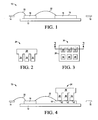
- FIG. 1 is a cross section of a power transistor device structure at a stage in processing
- FIG. 2 is a cross section of a heat spreading structure useful in the power transistor device structure of FIG. 1 ;
- FIG. 3 is a bottom view of the heat spreading structure of FIG. 2 ;
- FIG. 4 is a cross section of the power transistor device structure of FIG. 1 at a subsequent stage in processing including mounting the heat spreading structure of FIG. 2 ;
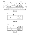
- FIG. 5 is a cross section of the power transistor device structure of FIG. 4 at a subsequent stage in processing
- FIG. 6 is a top view of the power transistor device structure of FIG. 5 ;
- FIG. 7 is a top view of the power transistor device structure of FIG. 5 and 6 at a subsequent stage in processing
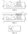
- FIG. 8 is a cross section of the power transistor device structure of FIG. 7 ;
- FIG. 9 is a cross section of the power transistor device structure of FIG. 8 after being mounted to a printed circuit board.
- FIG. 10 is a simplified top view of the die of FIGs. 1 and 4-9 having a power transistor.
- a power die having at least one power transistor is mounted to a package substrate.
- a heat spreader of metal that is shaped similar to a table having a tabletop and legs. The legs are attached to electrical connections on the power die. Encapsulation is performed so that the tabletop is exposed and is coplanar with a top surface of the encapsulant. The tabletop is then partitioned so that the electrical connections of the power die are individually extended to the top surface of the encapsulant as portions of the tabletop. The portions of the tabletop then may conveniently be attached to a printed circuit board. This results in contacts for the power die being relatively large metal portions from the metal tabletop so that current density is reduced and power is dissipated.
- FIG. 1 Shown in FIG. 1 is a power transistor device structure 10 having a package substrate 12 that may be a flag, a lead 14, a lead 15, a control integrated circuit 16 mounted on a top side of substrate 12, a power die 18 having an active surface 19, a wire bond 20 electrically connecting lead 14 to integrated circuit 16, and a wire bond 22 electrically connecting power die 18 to control integrated circuit 16.
- the control of power die 18 is achieved through control integrated circuit 16 in this example.
- Lead 15 may not necessarily be electrically connected but forms part of a leadframe that supports substrate 12.
- the leadframe as shown in FIG. 1 which is conventional, comprises substrate 12, lead 14, and lead 15 and further includes other leads and connections not shown in FIG. 1 .
- Power die 18 includes at least one power transistor and may be considered an integrated circuit die.
- FIG. 2 Shown in FIG. 2 , as a cross section, is a heat spreading structure 24 that is metal, which may be copper, and formed in a shape similar to that of a table.
- a heat spreading structure 24 that is metal, which may be copper, and formed in a shape similar to that of a table.
- FIG. 2 which is a cross section, is a continuous top portion that may be referenced as tabletop 26 and separate portions extending downward from tabletop 26 that may be referenced as legs 28, 30, and 32.
- FIG. 3 Shown in FIG. 3 , as a bottom view and showing the location of the cross section of FIG. 2 , is heat spreading structure 24 further showing legs 34, 36, and 38.
- Legs 28, 30, 32, 34, 36, and 38 may each have a square cross section. Square is likely to be the most efficient way but round rectangular may also be effective. The dimensions can vary but are likely to be in the millmeter range. One example may be of about 1 millimeter (mm) square for the cross section and a height of about 2 mm. Another example may be 0.5 mm square. The height can vary as well.
- FIG. 4 Shown in FIG. 4 is power transistor device structure 10 after mounting heat spreading structure 24 after mounting legs 28, 30, and 32, to power die 18 with attachment material 40, 42, and 44, respectively. Legs 34, 36, and 38 are also mounted to power die 18 but are not shown in this cross section.
- the attachment materials 40, 42, and 44 are both electrically and thermally conductive and may be a conductive adhesive. Other connecting techniques such as solder may be used.
- Power die 18 is designed so that external connections are aligned to legs 28, 30, 32, 34, 36, and 38.
- the attachment material could also be solder to improve performance but is likely to increase cost, especially in modifying the die.
- FIG. 5 Shown in FIG. 5 is power transistor device structure 10 after an encapsulation that results in an encapsulant 46 having a top surface 48 that is flat and coplanar with a top surface of tabletop 26 which is also flat. Leads such as leads 14 and 15 are partially within encapsulant 46 and partially extend from encapsulant 46.
- FIG. 6 Shown in FIG. 6 is a top view of power transistor device structure 10 as shown in FIG. 5 . This shows top surface 50 of tabletop 26 and top surface 48 of encapsulant 46.
- FIG. 7 Shown in FIG. 7 is a top view of power transistor device structure 10 after forming grooves 52, 54, and 56 to result in external contacts 58, 60, 62, 64, 66, and 68 from tabletop 26.
- Grooves 52, 54, and 56 may be formed using a tool that is used in singulating die with an appropriate depth setting to ensure that tabletop 26 is cut through but not so deep as to result in any damage to other portions of the power transistor device structure 10. It may be important to ensure that wire bonds are not in the path of the groove formation.
- groove 52 is may be considered to be in the X-direction and and grooves 54 and 56 may be considered to be in the Y-direction.
- the removing of the portions of tabletop 26 to form external contacts 58, 60, 62, 64, 66, and 68 may also be done by other means than cutting such as using a laser.
- FIG. 8 Shown in FIG. 8 is a cross section view similar to that of FIGs. 1, 4 , and 5 but at the same stage in processing as shown in FIG. 7 .
- This shows three connections from power die 18 to external to power transistor device structure 10; a first of which is through attachment material 40, leg 28, and external contact 58; a second of which is through attachment material 42, leg 30, and external contact 60; and a third of which is through attachment material 44, leg 32, and external contact 62.
- This also shows that grooves 54 and 56 extend sufficiently that external contacts 58, 60, and 62 are separated from each other.
- FIG. 9 Shown in FIG. 9 is a mounted power device 70 after connecting power transistor device structure 10 to a printed circuit board 72 having bond pads 74, 76, and 78. External contact 58 is connected to bond pad 74 with attachment material 80. External contact 60 is connected to bond pad 76 with attachment material 82. External contact 62 is connected to bond pad 78 with attachment material 84. Leads not shown in the FIGs. would also be attached to printed circuit board 72 to hold power transistor device structure 10 in place.
- FIG. 10 Shown in FIG. 10 is die 18 showing an exemplary power transistor 90 having a control electrode coupled to wire bond 22, a first current electrode coupled to attachment material 40, and a second current electrode coupled to attachment material 42.
- Other connections using attachment material, legs, and external contacts may also be implemented for other aspects of die 18 such as other transistors, power, and ground.
- Another approach is to attach separate posts in place of legs extending from a tabletop and the forming grooves to break up the tabletop. In such case each post would be separated from the other posts at the time of attachment to the power die. Encapsulation would thus occur with the posts separated and no groove making step would be required.
- the groove approach appears to provide benefits for stability of placement of the contacts and during encapsulation.
- the method further includes attaching a heat spreader to an active surface of the power die, wherein the heat spreader is thermally and electrically conductive, the active surface includes bond pads that are electrically conductive, and the heat spreader includes a flat surface and a plurality of legs attached to one side of the flat surface, each of the legs are attached to a corresponding one of the bond pads.
- the method further includes molding an encapsulating material to surround the power die, the leadframe, and the legs of the heat spreader, wherein a top side of the flat surface is exposed through the encapsulating material.
- the method further includes cutting through the flat surface between the legs to form external contacts that are electrically independent of one another.
- the method may have a further characterization by which the attaching the heat spreader to the leadframe includes using at least one of: a conductive adhesive and a conductive bond.
- the method may further include the cutting through the flat surface includes using one of a group consisting of: a mechanical saw and a laser.
- the method may further include forming the legs on the heat spreader by using at least one of the group consisting of: chemical etching, a laser, a punch press, and a mechanical saw.
- the method may have a further characterization by which the top side of the flat surface is coplanar with a top surface (48) of the encapsulating material.
- the method may further include attaching a control die to the leadframe and forming a wire bond between the control die and the power die.
- the method may further include attaching the external contacts to corresponding electrical contacts on a circuit board.
- the method may have a further characterization by which one of the external contacts conducts a signal from a power transistor in the power die.
- the method may have a further characterization by which the attaching the heat spreader to the circuit board includes using at least one of: an electrically conductive adhesive and an electrically conductive bond.
- a method that includes attaching a die to a substrate.
- the method further includes attaching a first end of each of a plurality of legs to an active surface of the die, wherein each of the plurality of legs is thermally and electrically conductive and the active surface includes a plurality of electrically conductive bond pads, each first end of the legs is attached to a corresponding one of the bond pads.
- the method further includes encapsulating the die and at least part of the legs in a mold compound, wherein each of the legs form at least part of a corresponding one of a plurality of external contacts that are exposed through the mold compound.
- the method may have a further characterization by which a second end of each of the legs is attached to a surface, the attaching the first end of the legs to the bond pads is performed while each of the second end of the legs is attached to the surface, and one side of the surface is exposed after the encapsulating and the method may further include, after the encapsulating, removing at least a portion of the surface between the legs to form the external contacts, wherein the external contacts are electrically independent of one another.
- the method may have a further characterization by which the first end of the legs has an exposed surface area that is between 50 and 100 percent of a contact area of the corresponding bond pads.
- the method may have a further characterization by which the legs retain the same shape before and after the legs are attached to the bond pads of the die.
- the method may have a further characterization by which the attaching the legs to the substrate includes using at least one of: a conductive adhesive and a conductive bond.
- the method may further include the removing at least a portion of the surface between the legs to form the external contacts includes using one of a group consisting of: a mechanical saw and a laser.
- the method may have a further characterization by which the die is a power die and one of the external contacts conducts a signal from a transistor in the die.
- a device that includes a substrate.
- the device further includes an integrated circuit (IC) die attached to the substrate on one side.
- the device further includes a plurality of contact pads on an active side of the IC die.
- the device further includes a plurality of legs that are thermally and electrically conductive, each of the legs attached to a respective one of the contact pads.
- the device further includes an encapsulating material formed around the substrate, the IC die, and a portion of the legs, a contact end of each of the legs is exposed, and one of the contact ends conducts a signal from a transistor in the IC die.
- the device may further include another one of the contact ends is coupled between a power supply and the transistor in the IC die.
- the device may have a further characterization by which the IC die is a power die.
- the device may further include the legs are attached to the contact pads using one of a group consisting of a conductive adhesive and a conductive bond.
- Coupled is not intended to be limited to a direct coupling or a mechanical coupling.
Landscapes
- Lead Frames For Integrated Circuits (AREA)
- Cooling Or The Like Of Semiconductors Or Solid State Devices (AREA)
- Chemical & Material Sciences (AREA)
- Engineering & Computer Science (AREA)
- Materials Engineering (AREA)
Abstract
Description
- This disclosure relates generally to power transistors, and more specifically, to power transistors with heat dissipation.
- Power transistors typically generate a significant amount of heat due to some combination of high heat and high current. The ability to dissipate that heat can be very significant in the ability to maintain a functional power transistor over the expected life of the product that uses the power transistor. Also reliability can be an extremely significant issue in some products such as automotive products. The heat itself can become destructive as can high current density even independent of the heat. Current and heat are related, but if the current density becomes too high, degradation at joints in the conductive path can degenerate and eventually fail.
- Accordingly there is a need to provide a power transistor with heat dissipation that improves upon one or more of the issues raised above.
- The present invention is illustrated by way of example and is not limited by the accompanying figures, in which like references indicate similar elements. Elements in the figures are illustrated for simplicity and clarity and have not necessarily been drawn to scale.
-
FIG. 1 is a cross section of a power transistor device structure at a stage in processing; -
FIG. 2 is a cross section of a heat spreading structure useful in the power transistor device structure ofFIG. 1 ; -
FIG. 3 is a bottom view of the heat spreading structure ofFIG. 2 ; -
FIG. 4 is a cross section of the power transistor device structure ofFIG. 1 at a subsequent stage in processing including mounting the heat spreading structure ofFIG. 2 ; -
FIG. 5 is a cross section of the power transistor device structure ofFIG. 4 at a subsequent stage in processing; -
FIG. 6 is a top view of the power transistor device structure ofFIG. 5 ; -
FIG. 7 is a top view of the power transistor device structure ofFIG. 5 and 6 at a subsequent stage in processing; -
FIG. 8 is a cross section of the power transistor device structure ofFIG. 7 ; -
FIG. 9 is a cross section of the power transistor device structure ofFIG. 8 after being mounted to a printed circuit board; and -
FIG. 10 is a simplified top view of the die ofFIGs. 1 and4-9 having a power transistor. - In one aspect, a power die having at least one power transistor is mounted to a package substrate. A heat spreader of metal that is shaped similar to a table having a tabletop and legs. The legs are attached to electrical connections on the power die. Encapsulation is performed so that the tabletop is exposed and is coplanar with a top surface of the encapsulant. The tabletop is then partitioned so that the electrical connections of the power die are individually extended to the top surface of the encapsulant as portions of the tabletop. The portions of the tabletop then may conveniently be attached to a printed circuit board. This results in contacts for the power die being relatively large metal portions from the metal tabletop so that current density is reduced and power is dissipated.
- Shown in
FIG. 1 is a powertransistor device structure 10 having apackage substrate 12 that may be a flag, alead 14, alead 15, a control integratedcircuit 16 mounted on a top side ofsubstrate 12, a power die 18 having anactive surface 19, awire bond 20 electrically connectinglead 14 to integratedcircuit 16, and awire bond 22 electrically connectingpower die 18 to control integratedcircuit 16. The control of power die 18 is achieved through control integratedcircuit 16 in this example.Lead 15 may not necessarily be electrically connected but forms part of a leadframe that supportssubstrate 12. The leadframe as shown inFIG. 1 , which is conventional, comprisessubstrate 12,lead 14, andlead 15 and further includes other leads and connections not shown inFIG. 1 . Power die 18 includes at least one power transistor and may be considered an integrated circuit die. - Shown in
FIG. 2 , as a cross section, is aheat spreading structure 24 that is metal, which may be copper, and formed in a shape similar to that of a table. In the portion shown inFIG. 2 , which is a cross section, is a continuous top portion that may be referenced astabletop 26 and separate portions extending downward fromtabletop 26 that may be referenced aslegs - Shown in
FIG. 3 , as a bottom view and showing the location of the cross section ofFIG. 2 , isheat spreading structure 24 further showinglegs legs legs legs Legs - Shown in
FIG. 4 is powertransistor device structure 10 after mountingheat spreading structure 24 after mountinglegs attachment material Legs attachment materials legs - Shown in
FIG. 5 is powertransistor device structure 10 after an encapsulation that results in an encapsulant 46 having atop surface 48 that is flat and coplanar with a top surface oftabletop 26 which is also flat. Leads such as leads 14 and 15 are partially withinencapsulant 46 and partially extend fromencapsulant 46. - Shown in
FIG. 6 is a top view of powertransistor device structure 10 as shown inFIG. 5 . This showstop surface 50 oftabletop 26 andtop surface 48 ofencapsulant 46. - Shown in
FIG. 7 is a top view of powertransistor device structure 10 after forminggrooves external contacts tabletop 26.Grooves tabletop 26 is cut through but not so deep as to result in any damage to other portions of the powertransistor device structure 10. It may be important to ensure that wire bonds are not in the path of the groove formation. In the orientation shown inFIG. 7 ,groove 52 is may be considered to be in the X-direction and andgrooves tabletop 26 to formexternal contacts - Shown in
FIG. 8 is a cross section view similar to that ofFIGs. 1, 4 , and5 but at the same stage in processing as shown inFIG. 7 . This shows three connections from power die 18 to external to powertransistor device structure 10; a first of which is throughattachment material 40,leg 28, andexternal contact 58; a second of which is throughattachment material 42,leg 30, andexternal contact 60; and a third of which is throughattachment material 44,leg 32, andexternal contact 62. This also shows thatgrooves external contacts - Shown in
FIG. 9 is a mountedpower device 70 after connecting powertransistor device structure 10 to a printedcircuit board 72 havingbond pads External contact 58 is connected tobond pad 74 withattachment material 80.External contact 60 is connected tobond pad 76 withattachment material 82.External contact 62 is connected tobond pad 78 withattachment material 84. Leads not shown in the FIGs. would also be attached to printedcircuit board 72 to hold powertransistor device structure 10 in place. - Using the example that high current is conducted from power die 18 through
attachment material 40,leg 28, andexternal contact 58, current density is comparatively low because of the relatively large cross section ofleg 28 andexternal contact 58. This reduces void formation resulting from high current densities. Copper is a relatively good conductor compared to aluminum so that there is less voltage drop due to both the increased cross section and the increased conductivity of copper over aluminum. Further the relative large cross section results in beneficial heat dissipation. One or more of the benefits relating to heat dissipation, current density, and voltage drop, can be used to increase current capability, lifetime, and/or reliability. - Shown in
FIG. 10 is die 18 showing anexemplary power transistor 90 having a control electrode coupled towire bond 22, a first current electrode coupled toattachment material 40, and a second current electrode coupled toattachment material 42. Other connections using attachment material, legs, and external contacts may also be implemented for other aspects ofdie 18 such as other transistors, power, and ground. - Another approach is to attach separate posts in place of legs extending from a tabletop and the forming grooves to break up the tabletop. In such case each post would be separated from the other posts at the time of attachment to the power die. Encapsulation would thus occur with the posts separated and no groove making step would be required. The groove approach appears to provide benefits for stability of placement of the contacts and during encapsulation.
- By now it should be appreciated that there has been provided a method that includes attaching a power die to a leadframe. The method further includes attaching a heat spreader to an active surface of the power die, wherein the heat spreader is thermally and electrically conductive, the active surface includes bond pads that are electrically conductive, and the heat spreader includes a flat surface and a plurality of legs attached to one side of the flat surface, each of the legs are attached to a corresponding one of the bond pads. The method further includes molding an encapsulating material to surround the power die, the leadframe, and the legs of the heat spreader, wherein a top side of the flat surface is exposed through the encapsulating material. The method further includes cutting through the flat surface between the legs to form external contacts that are electrically independent of one another. The method may have a further characterization by which the attaching the heat spreader to the leadframe includes using at least one of: a conductive adhesive and a conductive bond. The method may further include the cutting through the flat surface includes using one of a group consisting of: a mechanical saw and a laser. The method may further include forming the legs on the heat spreader by using at least one of the group consisting of: chemical etching, a laser, a punch press, and a mechanical saw. The method may have a further characterization by which the top side of the flat surface is coplanar with a top surface (48) of the encapsulating material. The method may further include attaching a control die to the leadframe and forming a wire bond between the control die and the power die. The method may further include attaching the external contacts to corresponding electrical contacts on a circuit board. The method may have a further characterization by which one of the external contacts conducts a signal from a power transistor in the power die. The method may have a further characterization by which the attaching the heat spreader to the circuit board includes using at least one of: an electrically conductive adhesive and an electrically conductive bond.
- Also disclosed is a method that includes attaching a die to a substrate. The method further includes attaching a first end of each of a plurality of legs to an active surface of the die, wherein each of the plurality of legs is thermally and electrically conductive and the active surface includes a plurality of electrically conductive bond pads, each first end of the legs is attached to a corresponding one of the bond pads. The method further includes encapsulating the die and at least part of the legs in a mold compound, wherein each of the legs form at least part of a corresponding one of a plurality of external contacts that are exposed through the mold compound. The method may have a further characterization by which a second end of each of the legs is attached to a surface, the attaching the first end of the legs to the bond pads is performed while each of the second end of the legs is attached to the surface, and one side of the surface is exposed after the encapsulating and the method may further include, after the encapsulating, removing at least a portion of the surface between the legs to form the external contacts, wherein the external contacts are electrically independent of one another. The method may have a further characterization by which the first end of the legs has an exposed surface area that is between 50 and 100 percent of a contact area of the corresponding bond pads. The method may have a further characterization by which the legs retain the same shape before and after the legs are attached to the bond pads of the die. The method may have a further characterization by which the attaching the legs to the substrate includes using at least one of: a conductive adhesive and a conductive bond. The method may further include the removing at least a portion of the surface between the legs to form the external contacts includes using one of a group consisting of: a mechanical saw and a laser. The method may have a further characterization by which the die is a power die and one of the external contacts conducts a signal from a transistor in the die.
- Disclosed also is a device that includes a substrate. The device further includes an integrated circuit (IC) die attached to the substrate on one side. The device further includes a plurality of contact pads on an active side of the IC die. The device further includes a plurality of legs that are thermally and electrically conductive, each of the legs attached to a respective one of the contact pads. The device further includes an encapsulating material formed around the substrate, the IC die, and a portion of the legs, a contact end of each of the legs is exposed, and one of the contact ends conducts a signal from a transistor in the IC die. The device may further include another one of the contact ends is coupled between a power supply and the transistor in the IC die. The device may have a further characterization by which the IC die is a power die. The device may further include the legs are attached to the contact pads using one of a group consisting of a conductive adhesive and a conductive bond.
- Moreover, the terms "front," "back," "top," "bottom," "over," "under" and the like in the description and in the claims, if any, are used for descriptive purposes and not necessarily for describing permanent relative positions. It is understood that the terms so used are interchangeable under appropriate circumstances such that the embodiments of the invention described herein are, for example, capable of operation in other orientations than those illustrated or otherwise described herein.
- Although the invention is described herein with reference to specific embodiments, various modifications and changes can be made without departing from the scope of the present invention as set forth in the claims below. For example, other metals than copper may be found to be beneficial for the heat spreader. Accordingly, the specification and figures are to be regarded in an illustrative rather than a restrictive sense, and all such modifications are intended to be included within the scope of the present invention. Any benefits, advantages, or solutions to problems that are described herein with regard to specific embodiments are not intended to be construed as a critical, required, or essential feature or element of any or all the claims.
- The term "coupled," as used herein, is not intended to be limited to a direct coupling or a mechanical coupling.
- Furthermore, the terms "a" or "an," as used herein, are defined as one or more than one. Also, the use of introductory phrases such as "at least one" and "one or more" in the claims should not be construed to imply that the introduction of another claim element by the indefinite articles "a" or "an" limits any particular claim containing such introduced claim element to inventions containing only one such element, even when the same claim includes the introductory phrases "one or more" or "at least one" and indefinite articles such as "a" or "an." The same holds true for the use of definite articles.
- Unless stated otherwise, terms such as "first" and "second" are used to arbitrarily distinguish between the elements such terms describe. Thus, these terms are not necessarily intended to indicate temporal or other prioritization of such elements.
Claims (13)
- A method comprising:attaching a power die (18) to a leadframe (12);attaching a thermally and electrically conductive heat spreader(24) to an active surface of the power die, wherein
the active surface includes electrically conductive bond pads,
the heat spreader includes a flat surface (50) and a plurality of legs (28-38) attached to one side of the flat surface, each of the legs are attached to a corresponding one of the bond pads;molding an encapsulating material (46) to surround the power die, the leadframe, and the legs of the heat spreader, wherein a top side of the flat surface is exposed through the encapsulating material; andcutting through the flat surface between the legs to form external contacts that are electrically independent of one another. - The method of any preceding claim wherein:the attaching the heat spreader to the leadframe includes using at least one of: a conductive adhesive and a conductive bond.
- The method of any preceding claim further comprising:the cutting through the flat surface includes using one of a group consisting of: a mechanical saw and a laser.
- The method of any preceding claim further comprising:forming the legs on the heat spreader by using at least one of the group consisting of: chemical etching, a laser, a punch press, and a mechanical saw.
- The method of any preceding claim wherein the top side of the flat surface is coplanar with a top surface (48) of the encapsulating material.
- The method of any preceding claim further comprising:attaching a control die (16) to the leadframe; andforming a wire bond (22) between the control die and the power die.
- The method of any preceding claim further comprising:attaching the external contacts to corresponding electrical contacts (74-78) on a circuit board (72).
- The method of any preceding claim wherein:one of the external contacts conducts a signal from a power transistor in the power die.
- The method of any preceding claim wherein:the attaching the heat spreader to the circuit board includes using at least one of: an electrically conductive adhesive (40-44) and an electrically conductive bond.
- A device comprising:a substrate (12);an integrated circuit (IC) die (18) attached to the substrate on one side, and having an active side;a plurality of thermally and electrically conductive legs (28-32), each of the legs attached to the active side and resulting in external contacts (58, 60, 62) that are separated from each other;_andan encapsulating material (46) formed around the substrate, the IC die, and a portion of the legs, the external contacts are exposed, and one of the external contacts (58) conducts a signal from a transistor (90) in the IC die.
- The device of any preceding claim further comprising:another one of the contact ends is coupled between a power supply and the transistor in the IC die.
- The device of any preceding claim wherein:the IC die is a power die.
- The device of any preceding claim further comprising:the legs are attached (40, 42, 44) to integrated circuit die using one of a group consisting of a conductive adhesive and a conductive bond.
Applications Claiming Priority (1)
| Application Number | Priority Date | Filing Date | Title |
|---|---|---|---|
| US13/538,585 US8790964B2 (en) | 2012-06-29 | 2012-06-29 | Power transistor with heat dissipation and method therefor |
Related Parent Applications (2)
| Application Number | Title | Priority Date | Filing Date |
|---|---|---|---|
| US13/538,585 Previously-Filed-Application US8790964B2 (en) | 2012-06-29 | 2012-06-29 | Power transistor with heat dissipation and method therefor |
| US201213538585 Previously-Filed-Application | 2012-06-29 |
Publications (2)
| Publication Number | Publication Date |
|---|---|
| EP2680306A1 true EP2680306A1 (en) | 2014-01-01 |
| EP2680306B1 EP2680306B1 (en) | 2019-01-09 |
Family
ID=48699559
Family Applications (1)
| Application Number | Title | Priority Date | Filing Date |
|---|---|---|---|
| EP13172879.2A Active EP2680306B1 (en) | 2012-06-29 | 2013-06-19 | Power transistor with heat dissipation and method therefore |
Country Status (3)
| Country | Link |
|---|---|
| US (2) | US8790964B2 (en) |
| EP (1) | EP2680306B1 (en) |
| CN (1) | CN103531564B (en) |
Cited By (1)
| Publication number | Priority date | Publication date | Assignee | Title |
|---|---|---|---|---|
| IT201700055921A1 (en) * | 2017-05-23 | 2018-11-23 | St Microelectronics Srl | SEMICONDUCTOR, CIRCUIT AND CORRESPONDENT PROCEDURE |
Families Citing this family (4)
| Publication number | Priority date | Publication date | Assignee | Title |
|---|---|---|---|---|
| US8790964B2 (en) * | 2012-06-29 | 2014-07-29 | Freescale Semiconductor, Inc. | Power transistor with heat dissipation and method therefor |
| KR20140018089A (en) * | 2012-07-25 | 2014-02-12 | 삼성전자주식회사 | Method and apparatus for traffic offloading to alleviate user plane congestion in wireless communication systtem |
| ITTO20120854A1 (en) * | 2012-09-28 | 2014-03-29 | Stmicroelectronics Malta Ltd | PERFORMED SURFACE MOUNTED CONTAINER FOR AN INTEGRATED SEMICONDUCTOR DEVICE, ITS ASSEMBLY AND MANUFACTURING PROCEDURE |
| US11972999B2 (en) * | 2021-12-07 | 2024-04-30 | Globalfoundries U.S. Inc. | Unlanded thermal dissipation pillar adjacent active contact |
Citations (2)
| Publication number | Priority date | Publication date | Assignee | Title |
|---|---|---|---|---|
| US20070296077A1 (en) * | 2006-06-27 | 2007-12-27 | Hvvi Semiconductors, Inc. | Semiconductor component and method of manufacture |
| US7851897B1 (en) * | 2008-06-16 | 2010-12-14 | Maxim Integrated Products, Inc. | IC package structures for high power dissipation and low RDSon |
Family Cites Families (19)
| Publication number | Priority date | Publication date | Assignee | Title |
|---|---|---|---|---|
| WO1994029900A1 (en) * | 1993-06-09 | 1994-12-22 | Lykat Corporation | Heat dissipative means for integrated circuit chip package |
| US6218732B1 (en) | 1998-09-15 | 2001-04-17 | Texas Instruments Incorporated | Copper bond pad process |
| US6469381B1 (en) * | 2000-09-29 | 2002-10-22 | Intel Corporation | Carbon-carbon and/or metal-carbon fiber composite heat spreader |
| US6455924B1 (en) * | 2001-03-22 | 2002-09-24 | International Business Machines Corporation | Stress-relieving heatsink structure and method of attachment to an electronic package |
| US6891256B2 (en) | 2001-10-22 | 2005-05-10 | Fairchild Semiconductor Corporation | Thin, thermally enhanced flip chip in a leaded molded package |
| TW510034B (en) * | 2001-11-15 | 2002-11-11 | Siliconware Precision Industries Co Ltd | Ball grid array semiconductor package |
| TW552689B (en) * | 2001-12-21 | 2003-09-11 | Siliconware Precision Industries Co Ltd | High electrical characteristic and high heat dissipating BGA package and its process |
| US7196415B2 (en) * | 2002-03-22 | 2007-03-27 | Broadcom Corporation | Low voltage drop and high thermal performance ball grid array package |
| TW556469B (en) * | 2002-08-20 | 2003-10-01 | Via Tech Inc | IC package with an implanted heat-dissipation fin |
| JP3834023B2 (en) * | 2003-08-19 | 2006-10-18 | 株式会社東芝 | LSI package with interface module and heat sink used therefor |
| TW200636946A (en) * | 2005-04-12 | 2006-10-16 | Advanced Semiconductor Eng | Chip package and packaging process thereof |
| TWI283553B (en) * | 2005-04-21 | 2007-07-01 | Ind Tech Res Inst | Thermal enhanced low profile package structure and method for fabricating the same |
| US7821116B2 (en) | 2007-02-05 | 2010-10-26 | Fairchild Semiconductor Corporation | Semiconductor die package including leadframe with die attach pad with folded edge |
| US8018050B2 (en) * | 2007-11-01 | 2011-09-13 | National Semiconductor Corporation | Integrated circuit package with integrated heat sink |
| TW200939407A (en) * | 2008-03-13 | 2009-09-16 | Chipmos Technologies Inc | Multi-chip package structure and the method thereof |
| KR101095119B1 (en) * | 2009-08-19 | 2011-12-16 | 삼성전기주식회사 | Die package and its manufacturing method |
| US8294276B1 (en) * | 2010-05-27 | 2012-10-23 | Amkor Technology, Inc. | Semiconductor device and fabricating method thereof |
| CN102842515A (en) * | 2011-06-23 | 2012-12-26 | 飞思卡尔半导体公司 | Method for assembling semiconductor device |
| US8790964B2 (en) * | 2012-06-29 | 2014-07-29 | Freescale Semiconductor, Inc. | Power transistor with heat dissipation and method therefor |
-
2012
- 2012-06-29 US US13/538,585 patent/US8790964B2/en active Active
-
2013
- 2013-06-19 EP EP13172879.2A patent/EP2680306B1/en active Active
- 2013-06-28 CN CN201310267931.3A patent/CN103531564B/en active Active
-
2014
- 2014-07-15 US US14/331,724 patent/US9129930B2/en active Active
Patent Citations (2)
| Publication number | Priority date | Publication date | Assignee | Title |
|---|---|---|---|---|
| US20070296077A1 (en) * | 2006-06-27 | 2007-12-27 | Hvvi Semiconductors, Inc. | Semiconductor component and method of manufacture |
| US7851897B1 (en) * | 2008-06-16 | 2010-12-14 | Maxim Integrated Products, Inc. | IC package structures for high power dissipation and low RDSon |
Cited By (2)
| Publication number | Priority date | Publication date | Assignee | Title |
|---|---|---|---|---|
| IT201700055921A1 (en) * | 2017-05-23 | 2018-11-23 | St Microelectronics Srl | SEMICONDUCTOR, CIRCUIT AND CORRESPONDENT PROCEDURE |
| US10756005B2 (en) | 2017-05-23 | 2020-08-25 | Stmicroelectronics S.R.L. | Semiconductor device, corresponding circuit and method |
Also Published As
| Publication number | Publication date |
|---|---|
| US20140001655A1 (en) | 2014-01-02 |
| US9129930B2 (en) | 2015-09-08 |
| CN103531564A (en) | 2014-01-22 |
| EP2680306B1 (en) | 2019-01-09 |
| US20140327124A1 (en) | 2014-11-06 |
| US8790964B2 (en) | 2014-07-29 |
| CN103531564B (en) | 2017-12-22 |
Similar Documents
| Publication | Publication Date | Title |
|---|---|---|
| TWI281238B (en) | Thermal enhanced package for block mold assembly | |
| CN101548377B (en) | Packaged integrated circuit with enhanced thermal dissipation | |
| US9029194B2 (en) | Making an integrated circuit module with dual leadframes | |
| KR101388328B1 (en) | Lead frame based, over-molded semiconductor package with integrated through hole technology(tht) heat spreader pin(s) and associated method of manufacturing | |
| JP5442368B2 (en) | IC chip package with direct lead wire | |
| US7495323B2 (en) | Semiconductor package structure having multiple heat dissipation paths and method of manufacture | |
| US8575742B1 (en) | Semiconductor device with increased I/O leadframe including power bars | |
| US9129930B2 (en) | Power transistor with heat dissipation and method therefore | |
| TW201448073A (en) | Semiconductor device manufacturing method | |
| US9484289B2 (en) | Semiconductor device with heat spreader | |
| US20140353766A1 (en) | Small Footprint Semiconductor Package | |
| US8946881B2 (en) | High-voltage packaged device | |
| EP3882969B1 (en) | A cascode semiconductor device and method of manufacture | |
| KR101162503B1 (en) | Heat slug and semiconductor package using the same | |
| US20200343167A1 (en) | Leaded Semiconductor Package | |
| CN102054717A (en) | Semiconductor chip grid array package and manufacturing method thereof | |
| US20060145312A1 (en) | Dual flat non-leaded semiconductor package | |
| US20240363484A1 (en) | Thermoelectric cooling for package level thermal management | |
| KR102260622B1 (en) | Qfn package with improved heat characteristic | |
| JPH03276667A (en) | Semiconductor device and manufacture thereof and applicable leadframe thereto | |
| KR101478759B1 (en) | Manufacturing method of substrate frame and manufacturing method of semiconductor device comprising the same | |
| US20090233403A1 (en) | Dual flat non-leaded semiconductor package | |
| KR101983164B1 (en) | Power Semi-Conductor package and Method of Manufacturing for the same | |
| CN205488099U (en) | Semiconductor device | |
| JPH09312371A (en) | Semiconductor device, manufacturing method thereof, and lead frame used for the same |
Legal Events
| Date | Code | Title | Description |
|---|---|---|---|
| PUAI | Public reference made under article 153(3) epc to a published international application that has entered the european phase |
Free format text: ORIGINAL CODE: 0009012 |
|
| AK | Designated contracting states |
Kind code of ref document: A1 Designated state(s): AL AT BE BG CH CY CZ DE DK EE ES FI FR GB GR HR HU IE IS IT LI LT LU LV MC MK MT NL NO PL PT RO RS SE SI SK SM TR |
|
| AX | Request for extension of the european patent |
Extension state: BA ME |
|
| 17P | Request for examination filed |
Effective date: 20140701 |
|
| RBV | Designated contracting states (corrected) |
Designated state(s): AL AT BE BG CH CY CZ DE DK EE ES FI FR GB GR HR HU IE IS IT LI LT LU LV MC MK MT NL NO PL PT RO RS SE SI SK SM TR |
|
| 17Q | First examination report despatched |
Effective date: 20150810 |
|
| RAP1 | Party data changed (applicant data changed or rights of an application transferred) |
Owner name: NXP USA, INC. |
|
| GRAP | Despatch of communication of intention to grant a patent |
Free format text: ORIGINAL CODE: EPIDOSNIGR1 |
|
| STAA | Information on the status of an ep patent application or granted ep patent |
Free format text: STATUS: GRANT OF PATENT IS INTENDED |
|
| INTG | Intention to grant announced |
Effective date: 20180719 |
|
| GRAJ | Information related to disapproval of communication of intention to grant by the applicant or resumption of examination proceedings by the epo deleted |
Free format text: ORIGINAL CODE: EPIDOSDIGR1 |
|
| STAA | Information on the status of an ep patent application or granted ep patent |
Free format text: STATUS: EXAMINATION IS IN PROGRESS |
|
| GRAP | Despatch of communication of intention to grant a patent |
Free format text: ORIGINAL CODE: EPIDOSNIGR1 |
|
| STAA | Information on the status of an ep patent application or granted ep patent |
Free format text: STATUS: GRANT OF PATENT IS INTENDED |
|
| INTC | Intention to grant announced (deleted) | ||
| GRAS | Grant fee paid |
Free format text: ORIGINAL CODE: EPIDOSNIGR3 |
|
| GRAA | (expected) grant |
Free format text: ORIGINAL CODE: 0009210 |
|
| STAA | Information on the status of an ep patent application or granted ep patent |
Free format text: STATUS: THE PATENT HAS BEEN GRANTED |
|
| INTG | Intention to grant announced |
Effective date: 20181123 |
|
| AK | Designated contracting states |
Kind code of ref document: B1 Designated state(s): AL AT BE BG CH CY CZ DE DK EE ES FI FR GB GR HR HU IE IS IT LI LT LU LV MC MK MT NL NO PL PT RO RS SE SI SK SM TR |
|
| REG | Reference to a national code |
Ref country code: GB Ref legal event code: FG4D |
|
| REG | Reference to a national code |
Ref country code: CH Ref legal event code: EP Ref country code: AT Ref legal event code: REF Ref document number: 1088383 Country of ref document: AT Kind code of ref document: T Effective date: 20190115 |
|
| REG | Reference to a national code |
Ref country code: DE Ref legal event code: R096 Ref document number: 602013049460 Country of ref document: DE |
|
| REG | Reference to a national code |
Ref country code: IE Ref legal event code: FG4D |
|
| REG | Reference to a national code |
Ref country code: NL Ref legal event code: MP Effective date: 20190109 |
|
| REG | Reference to a national code |
Ref country code: LT Ref legal event code: MG4D |
|
| PG25 | Lapsed in a contracting state [announced via postgrant information from national office to epo] |
Ref country code: NL Free format text: LAPSE BECAUSE OF FAILURE TO SUBMIT A TRANSLATION OF THE DESCRIPTION OR TO PAY THE FEE WITHIN THE PRESCRIBED TIME-LIMIT Effective date: 20190109 |
|
| REG | Reference to a national code |
Ref country code: AT Ref legal event code: MK05 Ref document number: 1088383 Country of ref document: AT Kind code of ref document: T Effective date: 20190109 |
|
| PG25 | Lapsed in a contracting state [announced via postgrant information from national office to epo] |
Ref country code: FI Free format text: LAPSE BECAUSE OF FAILURE TO SUBMIT A TRANSLATION OF THE DESCRIPTION OR TO PAY THE FEE WITHIN THE PRESCRIBED TIME-LIMIT Effective date: 20190109 Ref country code: NO Free format text: LAPSE BECAUSE OF FAILURE TO SUBMIT A TRANSLATION OF THE DESCRIPTION OR TO PAY THE FEE WITHIN THE PRESCRIBED TIME-LIMIT Effective date: 20190409 Ref country code: PL Free format text: LAPSE BECAUSE OF FAILURE TO SUBMIT A TRANSLATION OF THE DESCRIPTION OR TO PAY THE FEE WITHIN THE PRESCRIBED TIME-LIMIT Effective date: 20190109 Ref country code: LT Free format text: LAPSE BECAUSE OF FAILURE TO SUBMIT A TRANSLATION OF THE DESCRIPTION OR TO PAY THE FEE WITHIN THE PRESCRIBED TIME-LIMIT Effective date: 20190109 Ref country code: ES Free format text: LAPSE BECAUSE OF FAILURE TO SUBMIT A TRANSLATION OF THE DESCRIPTION OR TO PAY THE FEE WITHIN THE PRESCRIBED TIME-LIMIT Effective date: 20190109 Ref country code: PT Free format text: LAPSE BECAUSE OF FAILURE TO SUBMIT A TRANSLATION OF THE DESCRIPTION OR TO PAY THE FEE WITHIN THE PRESCRIBED TIME-LIMIT Effective date: 20190509 Ref country code: SE Free format text: LAPSE BECAUSE OF FAILURE TO SUBMIT A TRANSLATION OF THE DESCRIPTION OR TO PAY THE FEE WITHIN THE PRESCRIBED TIME-LIMIT Effective date: 20190109 |
|
| PG25 | Lapsed in a contracting state [announced via postgrant information from national office to epo] |
Ref country code: LV Free format text: LAPSE BECAUSE OF FAILURE TO SUBMIT A TRANSLATION OF THE DESCRIPTION OR TO PAY THE FEE WITHIN THE PRESCRIBED TIME-LIMIT Effective date: 20190109 Ref country code: GR Free format text: LAPSE BECAUSE OF FAILURE TO SUBMIT A TRANSLATION OF THE DESCRIPTION OR TO PAY THE FEE WITHIN THE PRESCRIBED TIME-LIMIT Effective date: 20190410 Ref country code: HR Free format text: LAPSE BECAUSE OF FAILURE TO SUBMIT A TRANSLATION OF THE DESCRIPTION OR TO PAY THE FEE WITHIN THE PRESCRIBED TIME-LIMIT Effective date: 20190109 Ref country code: RS Free format text: LAPSE BECAUSE OF FAILURE TO SUBMIT A TRANSLATION OF THE DESCRIPTION OR TO PAY THE FEE WITHIN THE PRESCRIBED TIME-LIMIT Effective date: 20190109 Ref country code: IS Free format text: LAPSE BECAUSE OF FAILURE TO SUBMIT A TRANSLATION OF THE DESCRIPTION OR TO PAY THE FEE WITHIN THE PRESCRIBED TIME-LIMIT Effective date: 20190509 Ref country code: BG Free format text: LAPSE BECAUSE OF FAILURE TO SUBMIT A TRANSLATION OF THE DESCRIPTION OR TO PAY THE FEE WITHIN THE PRESCRIBED TIME-LIMIT Effective date: 20190409 |
|
| REG | Reference to a national code |
Ref country code: DE Ref legal event code: R097 Ref document number: 602013049460 Country of ref document: DE |
|
| PG25 | Lapsed in a contracting state [announced via postgrant information from national office to epo] |
Ref country code: AT Free format text: LAPSE BECAUSE OF FAILURE TO SUBMIT A TRANSLATION OF THE DESCRIPTION OR TO PAY THE FEE WITHIN THE PRESCRIBED TIME-LIMIT Effective date: 20190109 Ref country code: DK Free format text: LAPSE BECAUSE OF FAILURE TO SUBMIT A TRANSLATION OF THE DESCRIPTION OR TO PAY THE FEE WITHIN THE PRESCRIBED TIME-LIMIT Effective date: 20190109 Ref country code: AL Free format text: LAPSE BECAUSE OF FAILURE TO SUBMIT A TRANSLATION OF THE DESCRIPTION OR TO PAY THE FEE WITHIN THE PRESCRIBED TIME-LIMIT Effective date: 20190109 Ref country code: SK Free format text: LAPSE BECAUSE OF FAILURE TO SUBMIT A TRANSLATION OF THE DESCRIPTION OR TO PAY THE FEE WITHIN THE PRESCRIBED TIME-LIMIT Effective date: 20190109 Ref country code: CZ Free format text: LAPSE BECAUSE OF FAILURE TO SUBMIT A TRANSLATION OF THE DESCRIPTION OR TO PAY THE FEE WITHIN THE PRESCRIBED TIME-LIMIT Effective date: 20190109 Ref country code: RO Free format text: LAPSE BECAUSE OF FAILURE TO SUBMIT A TRANSLATION OF THE DESCRIPTION OR TO PAY THE FEE WITHIN THE PRESCRIBED TIME-LIMIT Effective date: 20190109 Ref country code: EE Free format text: LAPSE BECAUSE OF FAILURE TO SUBMIT A TRANSLATION OF THE DESCRIPTION OR TO PAY THE FEE WITHIN THE PRESCRIBED TIME-LIMIT Effective date: 20190109 Ref country code: IT Free format text: LAPSE BECAUSE OF FAILURE TO SUBMIT A TRANSLATION OF THE DESCRIPTION OR TO PAY THE FEE WITHIN THE PRESCRIBED TIME-LIMIT Effective date: 20190109 |
|
| PLBE | No opposition filed within time limit |
Free format text: ORIGINAL CODE: 0009261 |
|
| STAA | Information on the status of an ep patent application or granted ep patent |
Free format text: STATUS: NO OPPOSITION FILED WITHIN TIME LIMIT |
|
| PG25 | Lapsed in a contracting state [announced via postgrant information from national office to epo] |
Ref country code: SM Free format text: LAPSE BECAUSE OF FAILURE TO SUBMIT A TRANSLATION OF THE DESCRIPTION OR TO PAY THE FEE WITHIN THE PRESCRIBED TIME-LIMIT Effective date: 20190109 |
|
| 26N | No opposition filed |
Effective date: 20191010 |
|
| PG25 | Lapsed in a contracting state [announced via postgrant information from national office to epo] |
Ref country code: MC Free format text: LAPSE BECAUSE OF FAILURE TO SUBMIT A TRANSLATION OF THE DESCRIPTION OR TO PAY THE FEE WITHIN THE PRESCRIBED TIME-LIMIT Effective date: 20190109 |
|
| REG | Reference to a national code |
Ref country code: CH Ref legal event code: PL |
|
| GBPC | Gb: european patent ceased through non-payment of renewal fee |
Effective date: 20190619 |
|
| PG25 | Lapsed in a contracting state [announced via postgrant information from national office to epo] |
Ref country code: SI Free format text: LAPSE BECAUSE OF FAILURE TO SUBMIT A TRANSLATION OF THE DESCRIPTION OR TO PAY THE FEE WITHIN THE PRESCRIBED TIME-LIMIT Effective date: 20190109 |
|
| REG | Reference to a national code |
Ref country code: BE Ref legal event code: MM Effective date: 20190630 |
|
| PG25 | Lapsed in a contracting state [announced via postgrant information from national office to epo] |
Ref country code: TR Free format text: LAPSE BECAUSE OF FAILURE TO SUBMIT A TRANSLATION OF THE DESCRIPTION OR TO PAY THE FEE WITHIN THE PRESCRIBED TIME-LIMIT Effective date: 20190109 |
|
| PG25 | Lapsed in a contracting state [announced via postgrant information from national office to epo] |
Ref country code: IE Free format text: LAPSE BECAUSE OF NON-PAYMENT OF DUE FEES Effective date: 20190619 Ref country code: GB Free format text: LAPSE BECAUSE OF NON-PAYMENT OF DUE FEES Effective date: 20190619 |
|
| PG25 | Lapsed in a contracting state [announced via postgrant information from national office to epo] |
Ref country code: LU Free format text: LAPSE BECAUSE OF NON-PAYMENT OF DUE FEES Effective date: 20190619 Ref country code: BE Free format text: LAPSE BECAUSE OF NON-PAYMENT OF DUE FEES Effective date: 20190630 Ref country code: LI Free format text: LAPSE BECAUSE OF NON-PAYMENT OF DUE FEES Effective date: 20190630 Ref country code: CH Free format text: LAPSE BECAUSE OF NON-PAYMENT OF DUE FEES Effective date: 20190630 |
|
| PG25 | Lapsed in a contracting state [announced via postgrant information from national office to epo] |
Ref country code: FR Free format text: LAPSE BECAUSE OF NON-PAYMENT OF DUE FEES Effective date: 20190630 |
|
| PG25 | Lapsed in a contracting state [announced via postgrant information from national office to epo] |
Ref country code: CY Free format text: LAPSE BECAUSE OF FAILURE TO SUBMIT A TRANSLATION OF THE DESCRIPTION OR TO PAY THE FEE WITHIN THE PRESCRIBED TIME-LIMIT Effective date: 20190109 |
|
| PG25 | Lapsed in a contracting state [announced via postgrant information from national office to epo] |
Ref country code: HU Free format text: LAPSE BECAUSE OF FAILURE TO SUBMIT A TRANSLATION OF THE DESCRIPTION OR TO PAY THE FEE WITHIN THE PRESCRIBED TIME-LIMIT; INVALID AB INITIO Effective date: 20130619 Ref country code: MT Free format text: LAPSE BECAUSE OF FAILURE TO SUBMIT A TRANSLATION OF THE DESCRIPTION OR TO PAY THE FEE WITHIN THE PRESCRIBED TIME-LIMIT Effective date: 20190109 |
|
| PG25 | Lapsed in a contracting state [announced via postgrant information from national office to epo] |
Ref country code: MK Free format text: LAPSE BECAUSE OF FAILURE TO SUBMIT A TRANSLATION OF THE DESCRIPTION OR TO PAY THE FEE WITHIN THE PRESCRIBED TIME-LIMIT Effective date: 20190109 |
|
| P01 | Opt-out of the competence of the unified patent court (upc) registered |
Effective date: 20230725 |
|
| PGFP | Annual fee paid to national office [announced via postgrant information from national office to epo] |
Ref country code: DE Payment date: 20250619 Year of fee payment: 13 |
|
| REG | Reference to a national code |
Ref country code: DE Ref legal event code: R079 Ref document number: 602013049460 Country of ref document: DE Free format text: PREVIOUS MAIN CLASS: H01L0023495000 Ipc: H10W0070400000 |