EP2680115A2 - Electrode substrate and touch panel - Google Patents
Electrode substrate and touch panel Download PDFInfo
- Publication number
- EP2680115A2 EP2680115A2 EP20130173569 EP13173569A EP2680115A2 EP 2680115 A2 EP2680115 A2 EP 2680115A2 EP 20130173569 EP20130173569 EP 20130173569 EP 13173569 A EP13173569 A EP 13173569A EP 2680115 A2 EP2680115 A2 EP 2680115A2
- Authority
- EP
- European Patent Office
- Prior art keywords
- electrode
- pattern unit
- substrate
- present
- pattern
- Prior art date
- Legal status (The legal status is an assumption and is not a legal conclusion. Google has not performed a legal analysis and makes no representation as to the accuracy of the status listed.)
- Granted
Links
Images

Classifications
-
- H—ELECTRICITY
- H05—ELECTRIC TECHNIQUES NOT OTHERWISE PROVIDED FOR
- H05K—PRINTED CIRCUITS; CASINGS OR CONSTRUCTIONAL DETAILS OF ELECTRIC APPARATUS; MANUFACTURE OF ASSEMBLAGES OF ELECTRICAL COMPONENTS
- H05K1/00—Printed circuits
- H05K1/02—Details
-
- G—PHYSICS
- G06—COMPUTING OR CALCULATING; COUNTING
- G06F—ELECTRIC DIGITAL DATA PROCESSING
- G06F3/00—Input arrangements for transferring data to be processed into a form capable of being handled by the computer; Output arrangements for transferring data from processing unit to output unit, e.g. interface arrangements
- G06F3/01—Input arrangements or combined input and output arrangements for interaction between user and computer
- G06F3/03—Arrangements for converting the position or the displacement of a member into a coded form
- G06F3/041—Digitisers, e.g. for touch screens or touch pads, characterised by the transducing means
-
- H—ELECTRICITY
- H05—ELECTRIC TECHNIQUES NOT OTHERWISE PROVIDED FOR
- H05K—PRINTED CIRCUITS; CASINGS OR CONSTRUCTIONAL DETAILS OF ELECTRIC APPARATUS; MANUFACTURE OF ASSEMBLAGES OF ELECTRICAL COMPONENTS
- H05K1/00—Printed circuits
- H05K1/02—Details
- H05K1/0296—Conductive pattern lay-out details not covered by sub groups H05K1/02 - H05K1/0295
-
- H—ELECTRICITY
- H05—ELECTRIC TECHNIQUES NOT OTHERWISE PROVIDED FOR
- H05K—PRINTED CIRCUITS; CASINGS OR CONSTRUCTIONAL DETAILS OF ELECTRIC APPARATUS; MANUFACTURE OF ASSEMBLAGES OF ELECTRICAL COMPONENTS
- H05K3/00—Apparatus or processes for manufacturing printed circuits
- H05K3/02—Apparatus or processes for manufacturing printed circuits in which the conductive material is applied to the surface of the insulating support and is thereafter removed from such areas of the surface which are not intended for current conducting or shielding
- H05K3/06—Apparatus or processes for manufacturing printed circuits in which the conductive material is applied to the surface of the insulating support and is thereafter removed from such areas of the surface which are not intended for current conducting or shielding the conductive material being removed chemically or electrolytically, e.g. by photo-etch process
-
- G—PHYSICS
- G06—COMPUTING OR CALCULATING; COUNTING
- G06F—ELECTRIC DIGITAL DATA PROCESSING
- G06F2203/00—Indexing scheme relating to G06F3/00 - G06F3/048
- G06F2203/041—Indexing scheme relating to G06F3/041 - G06F3/045
- G06F2203/04103—Manufacturing, i.e. details related to manufacturing processes specially suited for touch sensitive devices
-
- G—PHYSICS
- G06—COMPUTING OR CALCULATING; COUNTING
- G06F—ELECTRIC DIGITAL DATA PROCESSING
- G06F2203/00—Indexing scheme relating to G06F3/00 - G06F3/048
- G06F2203/041—Indexing scheme relating to G06F3/041 - G06F3/045
- G06F2203/04112—Electrode mesh in capacitive digitiser: electrode for touch sensing is formed of a mesh of very fine, normally metallic, interconnected lines that are almost invisible to see. This provides a quite large but transparent electrode surface, without need for ITO or similar transparent conductive material
-
- H—ELECTRICITY
- H05—ELECTRIC TECHNIQUES NOT OTHERWISE PROVIDED FOR
- H05K—PRINTED CIRCUITS; CASINGS OR CONSTRUCTIONAL DETAILS OF ELECTRIC APPARATUS; MANUFACTURE OF ASSEMBLAGES OF ELECTRICAL COMPONENTS
- H05K1/00—Printed circuits
- H05K1/02—Details
- H05K1/0286—Programmable, customizable or modifiable circuits
- H05K1/0287—Programmable, customizable or modifiable circuits having an universal lay-out, e.g. pad or land grid patterns or mesh patterns
- H05K1/0289—Programmable, customizable or modifiable circuits having an universal lay-out, e.g. pad or land grid patterns or mesh patterns having a matrix lay-out, i.e. having selectively interconnectable sets of X-conductors and Y-conductors in different planes
-
- H—ELECTRICITY
- H05—ELECTRIC TECHNIQUES NOT OTHERWISE PROVIDED FOR
- H05K—PRINTED CIRCUITS; CASINGS OR CONSTRUCTIONAL DETAILS OF ELECTRIC APPARATUS; MANUFACTURE OF ASSEMBLAGES OF ELECTRICAL COMPONENTS
- H05K2203/00—Indexing scheme relating to apparatus or processes for manufacturing printed circuits covered by H05K3/00
- H05K2203/01—Tools for processing; Objects used during processing
- H05K2203/0104—Tools for processing; Objects used during processing for patterning or coating
- H05K2203/0113—Female die used for patterning or transferring, e.g. temporary substrate having recessed pattern
Definitions
- the present invention relates to an electrode substrate and touch panel, more specifically, to an electrode substrate and touch panel, which has excellent conductive and optical properties.
- a touch panel is installed on a display surface of an image display unit such as an LCD (Liquid Crystal Display) device, an FED (Field Emission Display) device, a PDP (Plasma Display Panel) and an ELD (Electro Luminescence Device), and is a device which is configured such that the user inputs predetermined information in a computer using the touch panel while showing the image display unit.
- an image display unit such as an LCD (Liquid Crystal Display) device, an FED (Field Emission Display) device, a PDP (Plasma Display Panel) and an ELD (Electro Luminescence Device)
- the touch panel has been widely used in communication terminals such as a smart phone or a touch phone for which touch commands are necessarily required.
- a transparent conductive component used in a display area of a touch panel has been produced by a deposition process for depositing an ITO (Indium Tin Oxide) on a transparent glass or film.
- ITO Indium Tin Oxide
- the ITO was used as a transparent electrode, and a low-resistance metal wiring electrode and an ITO transparent electrode pattern were formed by repeating a photolithography process several times.
- An aspect of the present invention provides an electrode substrate, which is configured such that a process is minimized by excluding a complex photolithography process upon manufacturing of the electrode substrate of the touch panel, and a nano fine electrode pattern is formed using a difference in etching speed caused by a difference in line width of patterns resulting from using a wet etching process to a metal material having an excellent electrical property, thereby enabling the electrode substrate of the touch panel to have more excellent conductive and optical properties than a conventional ITO electrode.
- Another aspect of the present invention provides an electrode substrate for a display device having flexibility.
- An electrode substrate comprising: a substrate; a first pattern unit on the substrate; and a second pattern unit on the substrate.
- the second pattern unit may have a width formed larger than that of the first pattern unit.
- the second pattern unit may have a height formed larger than that of the first pattern unit.
- At least one of the first pattern unit and the second pattern unit may be configured such that a height of the at least one is formed larger than a width thereof.
- the electrode substrate may further include an electrode formed of a metal material in an upper part of the second pattern unit.
- the electrode may have a height of 100 to 300 nm.
- the electrode may be a wiring electrode or a sensing electrode.
- the wiring electrode may have a width formed narrower than that of the sensing electrode.
- the width of the wiring electrode may be formed in the range of 20 ⁇ m to 40 ⁇ m.
- the width of the sensing electrode may be formed in the range of 500 nm to 5 ⁇ m.
- the first pattern unit may be a line pattern or an isolated pattern.
- the first pattern unit and the second pattern may be composed of a UV curing resin.
- a cross section of the plurality of pattern units has a shape having a curvature.
- a touch panel including at least one or more electrode substrates that comprise: a substrate; a first pattern unit on the substrate; and a second pattern unit on the substrate.
- the touch panel may further include a flexible printed circuit board (FPCB) for connecting the electrode substrates and a driving circuit.
- FPCB flexible printed circuit board
- the electrode substrates may be configured of a first electrode substrate and a second electrode substrate.
- the electrode substrates may be configured of a first surface or a second surface, and at least one of the first surface and the second surface may include the first pattern unit and the second pattern unit.
- a display device including: at least one or more electrode substrates that comprise: a substrate; a first pattern unit on the substrate; and a second pattern unit on the substrate; and a driving unit for driving the electrode substrates.
- the electrode substrate of the touch panel which has more excellent conductive and optical properties than a conventional ITO electrode, can be produced in such a manner that a process is minimized by excluding a complex photolithography process upon manufacturing of the electrode substrate of the touch panel, and a nano fine electrode pattern is formed using a difference in etching speed caused by a difference in line width of patterns resulting from using a wet etching process to a metal material having an excellent electrical property.
- the electrode substrate for a display device having flexibility can be produced.
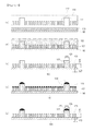
- FIG. 1 is a view for explaining a method of manufacturing an electrode substrate according to one embodiment of the present invention
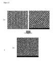
- FIG. 2 is a view illustrating a mold according to another embodiment of the present invention.
- FIG. 3 is a view illustrating a UV curing resin layer including a first pattern unit and a second pattern unit according to still another embodiment of the present invention
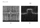
- FIG. 4 is a view in which a metal material is deposited on each upper part of the first pattern unit and the second pattern unit according to still further another embodiment.
- FIG. 5 is view in which an electrode according to still further another embodiment of the present invention is formed.
- FIG. 1 is a view for explaining a method of manufacturing an electrode substrate according to one embodiment of the present invention.
- a mold 110 includes a first mold pattern unit 111 and a second mold pattern unit 112. At this time, after the first mold pattern unit 111 is formed by a first process, the second mold pattern unit 112 is formed by a second process.
- the first mold pattern unit 111 is an element for forming a first pattern unit 121 illustrated in (b) of FIG. 1 through an imprinting process
- the second mold pattern unit 112 is an element for forming a second pattern unit 125 illustrated in (b) of FIG. 1 through an imprinting process.
- the mold 110 includes the first mold pattern unit 111 for forming the first pattern unit on an UV curing resin layer 105 and the second mold pattern unit 112 for forming the second pattern unit on the UV curing resin layer 105.
- the first mold pattern unit 111 may be formed using an E-beam method, an interference method or a spacer lithography method.
- the second mold pattern unit 112 may be formed using an E-beam method, a laser writing method or a photolithography method.
- the first pattern unit 121 and the second pattern unit 125 are formed by imprinting the mold 110 on the UV curing resin layer 105.
- the UV curing resin layer 105 is formed by coating a substrate 100 with an UV curing resin
- the UV curing resin is filled between the mold pattern units 111, 112 formed in the mold 110 by applying pressure to the UV curing resin layer 105 using the mold 110.
- a width 126 and a height 127 of the second pattern unit 125 are formed larger than a width 123 and a height 124 of the first pattern unit 121.
- a metal material 130 is deposited on each upper part of the first pattern unit 121 and the second pattern unit 125.
- the metal material 130 deposited on each upper part of the first pattern unit 121 and the second pattern unit 125 may have a height of 100 to 300 nm so that adjacent metal materials are not in contact with each other.
- the metal material 130 deposited on each upper part of the first pattern unit 121 is removed by the wet etching process.
- the metal material deposited on the upper part of the second pattern unit 125 is partially removed by the wet etching process, the metal material 130 is left, thereby forming an electrode 135.
- the formed electrode 135 may be a sensing electrode for sensing a touch command or a wiring electrode for transmitting a sensing signal from the sensing electrode.
- the electrode substrate of the touch panel includes the substrate 100, the first pattern unit 121, the second pattern unit 125 and the electrode 135.
- the first pattern unit 121 and the second pattern unit 125 are formed in an upper part of the substrate 100.
- the first pattern unit 121 and the second pattern unit 125 are formed of an UV curing resin. At this time, the width 126 and the height 127 of the second pattern unit 125 are formed larger than the width 123 or the height 124 of the first pattern unit 121.
- the electrode 135 composed of the metal material is formed in the upper part of the second pattern unit 125, which is formed as described above.
- the metal material is deposited on each upper part of the first pattern unit 121 and the second pattern unit 125, and thereafter, the wet etching process therefor is carried.
- the electrode 135 is formed. That is, according to the present embodiment of the invention, a nano fine electrode is formed using a difference in etching speed caused by a difference in line width between the patterns resulting from using the wet etching process to the metal material.
- the electrode 135, which is formed as described above, may be a sensing electrode for sensing a touch command or a wiring electrode for transmitting a sensing signal from the sensing electrode.
- the wiring electrode may have a width of 20 ⁇ m to 40 ⁇ m, and the sensing electrode may have a width of 500 nm to 5 ⁇ m.
- FIG. 2 is a view illustrating the mold according to another embodiment of the present invention.
- the first mold pattern unit is first formed.
- the first mold pattern unit may be formed using an E-beam method, an interference method or a spacer lithography method.
- the first mold pattern unit may be composed of line/space or dot patterns having a cycle of less than 1 ⁇ m through these process methods.
- the second mold pattern unit as illustrated in (b) of FIG. 2 is formed.
- the second mold pattern unit may be formed using an E-beam method, a laser writing method or photolithography method.
- the second mold pattern unit has a width (line) 20 ⁇ m to 40 ⁇ m at a part where the wiring electrode among the electrodes is formed, and has a width (line) of 500 nm to 5 ⁇ m at a part where the sensing electrode.
- FIG. 3 is a view illustrating the UV curing resin layer including the first pattern unit and the second pattern unit according to still another embodiment of the present invention
- FIG. 4 is a view in which the metal material is deposited on each upper part of the first pattern unit and the second pattern unit according to still further another embodiment
- FIG. 5 is view in which an electrode according to still further another embodiment of the present invention is formed.
- the UV curing resin layer is formed by coating the substrate with the UV curing resin
- the UV curing resin is filled between the mold pattern units formed in the mold by applying pressure to the UV curing resin layer using the mold, and the UV curing resin filled between the mold pattern units is cured by irradiating ultraviolet rays thereto, so the UV curing resin layer having the first pattern unit 121 and the second pattern unit 135 is formed as illustrated in FIG. 3 .
- the metal material is deposited on each upper part of the first pattern unit and the second pattern unit, and thus as illustrated in a cross-sectional view of (b) of FIG. 4 , it could be confirmed that the metal material 130 is deposited on each upper part of the first pattern unit and the second pattern unit.
- the wet etching process for the metal material is carried out.
- the metal material on the first pattern unit is completely removed, whereas the metal material of the upper part of the second pattern unit the electrode 135 is left, so the electrode 135 is formed due to the metal material.
- the electrode panel of the touch panel which has more excellent conductive and optical properties than the conventional ITO electrode, can be produced because the nano fine electrode pattern is formed using the difference in etching speed caused by the difference in line width between the patterns resulting from using the wet etching process to the metal material having an excellent electrical property.
Landscapes
- Engineering & Computer Science (AREA)
- General Engineering & Computer Science (AREA)
- Theoretical Computer Science (AREA)
- Microelectronics & Electronic Packaging (AREA)
- Human Computer Interaction (AREA)
- Physics & Mathematics (AREA)
- General Physics & Mathematics (AREA)
- Manufacturing & Machinery (AREA)
- Position Input By Displaying (AREA)
- Switches That Are Operated By Magnetic Or Electric Fields (AREA)
Abstract
Description
- This application claims priority to Korean Patent Application No.
10-2012-0069269, filed on June 27, 2012 - The present invention relates to an electrode substrate and touch panel, more specifically, to an electrode substrate and touch panel, which has excellent conductive and optical properties.
- A touch panel is installed on a display surface of an image display unit such as an LCD (Liquid Crystal Display) device, an FED (Field Emission Display) device, a PDP (Plasma Display Panel) and an ELD (Electro Luminescence Device), and is a device which is configured such that the user inputs predetermined information in a computer using the touch panel while showing the image display unit. Recently, the touch panel has been widely used in communication terminals such as a smart phone or a touch phone for which touch commands are necessarily required.
- In general, a transparent conductive component used in a display area of a touch panel has been produced by a deposition process for depositing an ITO (Indium Tin Oxide) on a transparent glass or film.
- More specifically, in the conventional touch panel, the ITO was used as a transparent electrode, and a low-resistance metal wiring electrode and an ITO transparent electrode pattern were formed by repeating a photolithography process several times.
- However, due to the recent short supply of indium, which is a main material of the ITO, it has been expected that a production cost will increase from now on. Also, a flexible display device having flexibility has been widely recognized as a leading product in future markets, but the ITO, which has been widely used, lacks flexibility, so it is problematic that the ITO is not appropriate for the flexible display device.
- In a way, researches for a method of implementing the display device using an Ag ink printing method for replacing the ITO electrode and reducing the production cost have been carried out. However, due to the securing of penetrability and electric resistance, the method is problematic.
- Accordingly, the present invention has been made keeping in mind the above problems occurring in the related art. An aspect of the present invention provides an electrode substrate, which is configured such that a process is minimized by excluding a complex photolithography process upon manufacturing of the electrode substrate of the touch panel, and a nano fine electrode pattern is formed using a difference in etching speed caused by a difference in line width of patterns resulting from using a wet etching process to a metal material having an excellent electrical property, thereby enabling the electrode substrate of the touch panel to have more excellent conductive and optical properties than a conventional ITO electrode.
- Another aspect of the present invention provides an electrode substrate for a display device having flexibility.
- According to an aspect of the present invention, there is provided An electrode substrate, comprising: a substrate; a first pattern unit on the substrate; and a second pattern unit on the substrate.
- According to one embodiment of the present invention, the second pattern unit may have a width formed larger than that of the first pattern unit.
- According to another embodiment of the present invention, the second pattern unit may have a height formed larger than that of the first pattern unit.
- According to still further another embodiment of the present invention, at least one of the first pattern unit and the second pattern unit may be configured such that a height of the at least one is formed larger than a width thereof.
- According to still further another embodiment of the present invention, the electrode substrate may further include an electrode formed of a metal material in an upper part of the second pattern unit.
- According to still further another embodiment of the present invention, the electrode may have a height of 100 to 300 nm.
- According to still further another embodiment of the present invention, the electrode may be a wiring electrode or a sensing electrode.
- According to still further another embodiment of the present invention, the wiring electrode may have a width formed narrower than that of the sensing electrode.
- According to still further another embodiment of the present invention, the width of the wiring electrode may be formed in the range of 20 µm to 40 µm.
- According to still further another embodiment of the present invention, the width of the sensing electrode may be formed in the range of 500 nm to 5 µm.
- According to still further another embodiment of the present invention, the first pattern unit may be a line pattern or an isolated pattern.
- According to still further another embodiment of the present invention, the first pattern unit and the second pattern may be composed of a UV curing resin.
- According to still further another embodiment of the present invention, a cross section of the plurality of pattern units has a shape having a curvature.
- According to another aspect of the present invention, there is provided a touch panel, including at least one or more electrode substrates that comprise: a substrate; a first pattern unit on the substrate; and a second pattern unit on the substrate.
- According to one embodiment of the present invention, the touch panel may further include a flexible printed circuit board (FPCB) for connecting the electrode substrates and a driving circuit.
- According to another embodiment of the present invention, the electrode substrates may be configured of a first electrode substrate and a second electrode substrate.
- According to still another embodiment of the present invention, the electrode substrates may be configured of a first surface or a second surface, and at least one of the first surface and the second surface may include the first pattern unit and the second pattern unit.
- According to still another aspect of the present invention, there is provided a display device, including: at least one or more electrode substrates that comprise: a substrate; a first pattern unit on the substrate; and a second pattern unit on the substrate; and a driving unit for driving the electrode substrates.
- According to the embodiments of the present invention, the electrode substrate of the touch panel, which has more excellent conductive and optical properties than a conventional ITO electrode, can be produced in such a manner that a process is minimized by excluding a complex photolithography process upon manufacturing of the electrode substrate of the touch panel, and a nano fine electrode pattern is formed using a difference in etching speed caused by a difference in line width of patterns resulting from using a wet etching process to a metal material having an excellent electrical property.
- Also, according to the embodiments of the present invention, the electrode substrate for a display device having flexibility can be produced.
- The accompanying drawings are included to provide a further understanding of the present invention, and are incorporated in and constitute a part of this specification. The drawings illustrate exemplary embodiments of the present invention and, together with the description, serve to explain principles of the present invention. In the drawings:
-
FIG. 1 is a view for explaining a method of manufacturing an electrode substrate according to one embodiment of the present invention; -
FIG. 2 is a view illustrating a mold according to another embodiment of the present invention; -
FIG. 3 is a view illustrating a UV curing resin layer including a first pattern unit and a second pattern unit according to still another embodiment of the present invention; -
FIG. 4 is a view in which a metal material is deposited on each upper part of the first pattern unit and the second pattern unit according to still further another embodiment; and -
FIG. 5 is view in which an electrode according to still further another embodiment of the present invention is formed. - Hereinafter, preferred embodiments of the present invention will be described in detail with reference to the accompanying drawings. In the following description, it is to be noted that, when the functions of conventional elements and the detailed description of elements related with the present invention may make the gist of the present invention unclear, a detailed description of those elements will be omitted. Further, it should be understood that the shape and size of the elements shown in the drawings may be exaggeratedly drawn to provide an easily understood description of the structure of the present invention rather than reflecting the actual sizes of the corresponding elements.
-
FIG. 1 is a view for explaining a method of manufacturing an electrode substrate according to one embodiment of the present invention. - The method of manufacturing the electrode substrate according to the present embodiment of the invention will be hereinafter explained with reference to
FIG. 1 . - As illustrated in (a) of
FIG. 1 , amold 110 according to the present embodiment of the invention includes a firstmold pattern unit 111 and a secondmold pattern unit 112. At this time, after the firstmold pattern unit 111 is formed by a first process, the secondmold pattern unit 112 is formed by a second process. - The first
mold pattern unit 111 is an element for forming afirst pattern unit 121 illustrated in (b) ofFIG. 1 through an imprinting process, and the secondmold pattern unit 112 is an element for forming asecond pattern unit 125 illustrated in (b) ofFIG. 1 through an imprinting process. - That is, the
mold 110 according to the present embodiment of the invention includes the firstmold pattern unit 111 for forming the first pattern unit on an UVcuring resin layer 105 and the secondmold pattern unit 112 for forming the second pattern unit on the UVcuring resin layer 105. - At this time, the first
mold pattern unit 111 may be formed using an E-beam method, an interference method or a spacer lithography method. The secondmold pattern unit 112 may be formed using an E-beam method, a laser writing method or a photolithography method. - After this, as illustrated in (b) of
FIG. 1 , thefirst pattern unit 121 and thesecond pattern unit 125 are formed by imprinting themold 110 on the UVcuring resin layer 105. - More specifically, when the UV
curing resin layer 105 is formed by coating asubstrate 100 with an UV curing resin, the UV curing resin is filled between themold pattern units mold 110 by applying pressure to the UVcuring resin layer 105 using themold 110. - After this, when the UV curing resin filled between the mold pattern units of the
mold 110 is cured by irradiating ultraviolet rays thereto, as illustrated in (c) ofFIG. 1 , thefirst pattern unit 121 and thesecond pattern unit 125 are formed. - At this time, a
width 126 and aheight 127 of thesecond pattern unit 125 are formed larger than awidth 123 and aheight 124 of thefirst pattern unit 121. - Hereinafter, as illustrated in (d) of
FIG. 1 , ametal material 130 is deposited on each upper part of thefirst pattern unit 121 and thesecond pattern unit 125. - At this time, the
metal material 130 deposited on each upper part of thefirst pattern unit 121 and thesecond pattern unit 125 may have a height of 100 to 300 nm so that adjacent metal materials are not in contact with each other. - After this, as illustrated in (e) of
FIG. 1 , a wet etching process for themetal material 130 deposited on each upper part of thefirst pattern unit 121 and thesecond pattern unit 125 are carried out. - At this time, the
metal material 130 deposited on each upper part of thefirst pattern unit 121 is removed by the wet etching process. However, since the metal material deposited on the upper part of thesecond pattern unit 125 is partially removed by the wet etching process, themetal material 130 is left, thereby forming anelectrode 135. - That is, since a difference in etching speed is generated due to a difference in line width between the first pattern unit 12 and the second pattern unit resulting from the wet etching process, the
metal material 130 of the upper part of thefirst pattern unit 121 is removed, but themetal material 130 of the upper part of thesecond pattern unit 125 is left so that the electrode is formed. At this time, the formedelectrode 135 may be a sensing electrode for sensing a touch command or a wiring electrode for transmitting a sensing signal from the sensing electrode. - Hereinafter, the configuration of the electrode substrate of the touch panel according to the present embodiment of the invention will be explained with reference to (e) of
FIG. 1 . - As illustrated in (e) of
FIG. 1 , the electrode substrate of the touch panel according to the present embodiment of the invention includes thesubstrate 100, thefirst pattern unit 121, thesecond pattern unit 125 and theelectrode 135. - The
first pattern unit 121 and thesecond pattern unit 125 are formed in an upper part of thesubstrate 100. - The
first pattern unit 121 and thesecond pattern unit 125 are formed of an UV curing resin. At this time, thewidth 126 and theheight 127 of thesecond pattern unit 125 are formed larger than thewidth 123 or theheight 124 of thefirst pattern unit 121. - The
electrode 135 composed of the metal material is formed in the upper part of thesecond pattern unit 125, which is formed as described above. In order to form theelectrode 135, the metal material is deposited on each upper part of thefirst pattern unit 121 and thesecond pattern unit 125, and thereafter, the wet etching process therefor is carried. Thus, only the metal material of the upper part of thesecond pattern unit 125 is left so theelectrode 135 is formed. That is, according to the present embodiment of the invention, a nano fine electrode is formed using a difference in etching speed caused by a difference in line width between the patterns resulting from using the wet etching process to the metal material. - In a way, the
electrode 135, which is formed as described above, may be a sensing electrode for sensing a touch command or a wiring electrode for transmitting a sensing signal from the sensing electrode. - At this time, when the nano fine electrode is formed using the difference in etching speed, the wiring electrode may have a width of 20 µm to 40 µm, and the sensing electrode may have a width of 500 nm to 5 µm.
- Like this, when the width of the wiring electrode is formed of the fine electrode of 20 µm to 40 µm, a bezel of the touch panel in which the electrode substrate according to the present embodiment of the invention is used may be minimized. When the width of the sensing electrode is formed in the range of 500 nm to 5 µm, the sensing electrode is not visible to the user's eye.
FIG. 2 is a view illustrating the mold according to another embodiment of the present invention. - According to the present embodiment of the invention, upon forming of the mold, as illustrated in (a) of
FIG. 2 , the first mold pattern unit is first formed. - At this time, the first mold pattern unit may be formed using an E-beam method, an interference method or a spacer lithography method. The first mold pattern unit may be composed of line/space or dot patterns having a cycle of less than 1 µm through these process methods.
- As described above, after the performing of the first process, the second mold pattern unit as illustrated in (b) of
FIG. 2 is formed. - The second mold pattern unit may be formed using an E-beam method, a laser writing method or photolithography method. The second mold pattern unit has a width (line) 20 µm to 40 µm at a part where the wiring electrode among the electrodes is formed, and has a width (line) of 500 nm to 5 µm at a part where the sensing electrode.
-
FIG. 3 is a view illustrating the UV curing resin layer including the first pattern unit and the second pattern unit according to still another embodiment of the present invention,FIG. 4 is a view in which the metal material is deposited on each upper part of the first pattern unit and the second pattern unit according to still further another embodiment, andFIG. 5 is view in which an electrode according to still further another embodiment of the present invention is formed. - When the UV curing resin layer is formed by coating the substrate with the UV curing resin, the UV curing resin is filled between the mold pattern units formed in the mold by applying pressure to the UV curing resin layer using the mold, and the UV curing resin filled between the mold pattern units is cured by irradiating ultraviolet rays thereto, so the UV curing resin layer having the
first pattern unit 121 and thesecond pattern unit 135 is formed as illustrated inFIG. 3 . - After this, as illustrated in (a) of
FIG. 4 , the metal material is deposited on each upper part of the first pattern unit and the second pattern unit, and thus as illustrated in a cross-sectional view of (b) ofFIG. 4 , it could be confirmed that themetal material 130 is deposited on each upper part of the first pattern unit and the second pattern unit. - After this, as illustrated in (a) of
FIG. 5 , the wet etching process for the metal material is carried out. Thus, as illustrated in a cross-sectional view of (b) ofFIG. 5 , the metal material on the first pattern unit is completely removed, whereas the metal material of the upper part of the second pattern unit theelectrode 135 is left, so theelectrode 135 is formed due to the metal material. - Accordingly, according to the embodiments of the present invention, the electrode panel of the touch panel, which has more excellent conductive and optical properties than the conventional ITO electrode, can be produced because the nano fine electrode pattern is formed using the difference in etching speed caused by the difference in line width between the patterns resulting from using the wet etching process to the metal material having an excellent electrical property.
- As previously described, in the detailed description of the invention, having described the detailed exemplary embodiments of the invention, it should be apparent that modifications and variations can be made by persons skilled without deviating from the spirit or scope of the invention. Therefore, it is to be understood that the foregoing is illustrative of the present invention and is not to be construed as limited to the specific embodiments disclosed, and that modifications to the disclosed embodiments, as well as other embodiments, are intended to be included within the scope of the appended claims and their equivalents.
Claims (12)
- An electrode substrate, comprising:a substrate;a first pattern unit on the substrate; anda second pattern unit on the substrate.
- The electrode substrate according to claim 1, wherein the second pattern unit has a width formed larger than that of the first pattern unit.
- The electrode substrate according to claim 1, further comprising an electrode formed of a metal material in an upper part of the second pattern unit.
- The electrode substrate according to claim 3, wherein the electrode has a height of 100 to 300 nm.
- The electrode substrate according to claim 3, wherein the electrode is a wiring electrode or a sensing electrode.
- The electrode substrate according to claim 5, wherein the wiring electrode has a width formed narrower than that of the sensing electrode.
- The electrode substrate according to claim 5, wherein the width of the wiring electrode is formed in the range of 20 µm to 40 µm.
- The electrode substrate according to claim 5, wherein the width of the sensing electrode is formed in the range of 500 nm to 5 µm.
- The electrode substrate according to claim 1, wherein the first pattern unit is a line pattern or an isolated pattern.
- The electrode substrate according to claim 1, wherein the first pattern unit and the second pattern are composed of a UV curing resin.
- A touch panel comprising at least one or more electrode substrates that comprise: a Substrate; a first pattern unit on the substrate; and a second pattern unit on the substrate.
- The touch panel according to 1 l, further comprising a flexible printed circuit board (FPCB) for connecting the electrode substrates and a driving circuit.
Applications Claiming Priority (1)
| Application Number | Priority Date | Filing Date | Title |
|---|---|---|---|
| KR1020120069269A KR20140001504A (en) | 2012-06-27 | 2012-06-27 | Electrode substrate of touch panel and manufacturing method thereof |
Publications (4)
| Publication Number | Publication Date |
|---|---|
| EP2680115A2 true EP2680115A2 (en) | 2014-01-01 |
| EP2680115A8 EP2680115A8 (en) | 2014-03-26 |
| EP2680115A3 EP2680115A3 (en) | 2014-11-19 |
| EP2680115B1 EP2680115B1 (en) | 2017-06-14 |
Family
ID=48699585
Family Applications (1)
| Application Number | Title | Priority Date | Filing Date |
|---|---|---|---|
| EP13173569.8A Not-in-force EP2680115B1 (en) | 2012-06-27 | 2013-06-25 | Electrode substrate and touch panel |
Country Status (6)
| Country | Link |
|---|---|
| US (1) | US9609735B2 (en) |
| EP (1) | EP2680115B1 (en) |
| JP (1) | JP5873045B2 (en) |
| KR (1) | KR20140001504A (en) |
| CN (1) | CN103529978B (en) |
| TW (1) | TWI605361B (en) |
Families Citing this family (4)
| Publication number | Priority date | Publication date | Assignee | Title |
|---|---|---|---|---|
| US10409432B2 (en) * | 2015-04-24 | 2019-09-10 | Lg Innotek Co., Ltd. | Touch window |
| KR101959488B1 (en) | 2015-09-08 | 2019-03-18 | 주식회사 엘지화학 | Method of manufacturing an optical device |
| KR102509067B1 (en) | 2016-04-08 | 2023-03-13 | 삼성디스플레이 주식회사 | User identifying device, input sensing module of the same and method for user identifying |
| CN107045407B (en) * | 2017-02-08 | 2019-05-17 | 维沃移动通信有限公司 | A touch screen and mobile terminal |
Family Cites Families (13)
| Publication number | Priority date | Publication date | Assignee | Title |
|---|---|---|---|---|
| EP1639632B1 (en) | 2003-05-16 | 2017-06-07 | Tokyo Electron Limited | Method of monitoring a processing system |
| JP4083638B2 (en) * | 2003-07-30 | 2008-04-30 | 東北パイオニア株式会社 | Flexible wiring board, semiconductor chip mounting flexible wiring board, display device, semiconductor chip mounting method |
| EP2257969B1 (en) * | 2008-02-28 | 2017-12-20 | 3M Innovative Properties Company | Methods of patterning a conductor on a substrate |
| KR101565798B1 (en) * | 2009-03-31 | 2015-11-05 | 삼성전자주식회사 | A semiconductor device having an integrated structure of a contact pad and a conductive line |
| KR20110001292A (en) * | 2009-06-30 | 2011-01-06 | 삼성전자주식회사 | Patterned Structure and Formation Method thereof |
| TWM387310U (en) | 2009-11-16 | 2010-08-21 | J Touch Corp | Improved circuit for transparent conductive panel and touch control panel |
| KR101726623B1 (en) * | 2010-03-16 | 2017-04-14 | 엘지디스플레이 주식회사 | Touch panel |
| CN201725318U (en) | 2010-05-16 | 2011-01-26 | 宸鸿科技(厦门)有限公司 | Capacitance touch control panel with low-visibility metal conductor |
| CN102222538B (en) * | 2011-03-11 | 2012-12-05 | 苏州纳格光电科技有限公司 | Graphical flexible transparent conductive film and preparation method thereof |
| JP5640854B2 (en) | 2011-03-25 | 2014-12-17 | ソニー株式会社 | Conductive element and manufacturing method thereof, wiring element, information input device, display device, electronic apparatus, and master |
| TWM425341U (en) | 2011-12-02 | 2012-03-21 | Young Fast Optoelectronics Co | Capacitive touch control device |
| TW201415067A (en) | 2012-03-28 | 2014-04-16 | Sony Corp | Conductive element and method of manufacture thereof, wiring element, and master |
| KR20130127848A (en) | 2012-05-15 | 2013-11-25 | 삼성전기주식회사 | Touch sensor and the manufacturing method |
-
2012
- 2012-06-27 KR KR1020120069269A patent/KR20140001504A/en not_active Withdrawn
-
2013
- 2013-06-25 EP EP13173569.8A patent/EP2680115B1/en not_active Not-in-force
- 2013-06-26 US US13/927,276 patent/US9609735B2/en not_active Expired - Fee Related
- 2013-06-27 TW TW102123016A patent/TWI605361B/en not_active IP Right Cessation
- 2013-06-27 CN CN201310261773.0A patent/CN103529978B/en not_active Expired - Fee Related
- 2013-06-27 JP JP2013134925A patent/JP5873045B2/en not_active Expired - Fee Related
Non-Patent Citations (1)
| Title |
|---|
| None |
Also Published As
| Publication number | Publication date |
|---|---|
| TW201411444A (en) | 2014-03-16 |
| CN103529978A (en) | 2014-01-22 |
| US9609735B2 (en) | 2017-03-28 |
| EP2680115B1 (en) | 2017-06-14 |
| TWI605361B (en) | 2017-11-11 |
| KR20140001504A (en) | 2014-01-07 |
| EP2680115A8 (en) | 2014-03-26 |
| JP2014010841A (en) | 2014-01-20 |
| CN103529978B (en) | 2016-09-07 |
| JP5873045B2 (en) | 2016-03-01 |
| EP2680115A3 (en) | 2014-11-19 |
| US20140000938A1 (en) | 2014-01-02 |
Similar Documents
| Publication | Publication Date | Title |
|---|---|---|
| CN102736780B (en) | Input device | |
| CN102622145B (en) | Projection type capacitive touch sensor structure and manufacturing method thereof | |
| EP2827231B1 (en) | Touch window and display including the same | |
| US10884548B2 (en) | Touch window and display with the same | |
| US20170045999A1 (en) | Touch window and touch device including the same | |
| US20150021156A1 (en) | Transparent conductive element and method for manufacturing the same, input device, electronic apparatus, and method for patterning thin film | |
| JP2015022768A (en) | Touch window and touch device including the same | |
| KR101956086B1 (en) | Touch panel, display and method of the same | |
| US9609735B2 (en) | Electrode substrate and touch panel | |
| KR101515376B1 (en) | Method for preparing touch screen panel and touch screen panel prepared from the same | |
| US9442613B2 (en) | Touch window | |
| US10437362B2 (en) | Touch window and display device comprising same | |
| US20150253903A1 (en) | Touch window and touch device including the same | |
| CN105487709A (en) | Touch screen and manufacturing method therefor | |
| KR101391306B1 (en) | Method of fabricating touch screen panel by printing method and touch screen panel manufactured by the same | |
| CN207198820U (en) | A kind of touch module, touching display screen and electronic equipment | |
| KR102237961B1 (en) | Touch window and display with the same | |
| KR102303068B1 (en) | Touch window | |
| KR102329718B1 (en) | Touch window | |
| KR102313957B1 (en) | Touch window | |
| KR102380881B1 (en) | Touch window | |
| KR102187657B1 (en) | Touch window and display with the same | |
| KR102303064B1 (en) | Touch window | |
| KR101154342B1 (en) | Touch panel for separating pattern layer and conductive layer, and the manufacturing method | |
| KR20160039426A (en) | Touch window |
Legal Events
| Date | Code | Title | Description |
|---|---|---|---|
| PUAI | Public reference made under article 153(3) epc to a published international application that has entered the european phase |
Free format text: ORIGINAL CODE: 0009012 |
|
| AK | Designated contracting states |
Kind code of ref document: A2 Designated state(s): AL AT BE BG CH CY CZ DE DK EE ES FI FR GB GR HR HU IE IS IT LI LT LU LV MC MK MT NL NO PL PT RO RS SE SI SK SM TR |
|
| AX | Request for extension of the european patent |
Extension state: BA ME |
|
| RIN1 | Information on inventor provided before grant (corrected) |
Inventor name: LEE, YOUNG JAE Inventor name: KIM, JIN SU Inventor name: YOO, KYOUNG JONG Inventor name: LEE, JUN |
|
| 17P | Request for examination filed |
Effective date: 20140328 |
|
| PUAL | Search report despatched |
Free format text: ORIGINAL CODE: 0009013 |
|
| AK | Designated contracting states |
Kind code of ref document: A3 Designated state(s): AL AT BE BG CH CY CZ DE DK EE ES FI FR GB GR HR HU IE IS IT LI LT LU LV MC MK MT NL NO PL PT RO RS SE SI SK SM TR |
|
| AX | Request for extension of the european patent |
Extension state: BA ME |
|
| RIC1 | Information provided on ipc code assigned before grant |
Ipc: H01L 29/06 20060101ALI20141013BHEP Ipc: H01L 21/30 20060101ALI20141013BHEP Ipc: G06F 3/041 20060101AFI20141013BHEP |
|
| RBV | Designated contracting states (corrected) |
Designated state(s): AL AT BE BG CH CY CZ DE DK EE ES FI FR GB GR HR HU IE IS IT LI LT LU LV MC MK MT NL NO PL PT RO RS SE SI SK SM TR |
|
| 17Q | First examination report despatched |
Effective date: 20160315 |
|
| GRAP | Despatch of communication of intention to grant a patent |
Free format text: ORIGINAL CODE: EPIDOSNIGR1 |
|
| INTG | Intention to grant announced |
Effective date: 20170118 |
|
| RIC1 | Information provided on ipc code assigned before grant |
Ipc: H01L 29/06 20060101ALI20170109BHEP Ipc: H01L 21/30 20060101ALI20170109BHEP Ipc: G06F 3/041 20060101AFI20170109BHEP Ipc: H05K 3/06 20060101ALN20170109BHEP |
|
| GRAS | Grant fee paid |
Free format text: ORIGINAL CODE: EPIDOSNIGR3 |
|
| GRAA | (expected) grant |
Free format text: ORIGINAL CODE: 0009210 |
|
| RAP1 | Party data changed (applicant data changed or rights of an application transferred) |
Owner name: LG INNOTEK CO., LTD. |
|
| AK | Designated contracting states |
Kind code of ref document: B1 Designated state(s): AL AT BE BG CH CY CZ DE DK EE ES FI FR GB GR HR HU IE IS IT LI LT LU LV MC MK MT NL NO PL PT RO RS SE SI SK SM TR |
|
| REG | Reference to a national code |
Ref country code: GB Ref legal event code: FG4D |
|
| REG | Reference to a national code |
Ref country code: CH Ref legal event code: EP Ref country code: AT Ref legal event code: REF Ref document number: 901565 Country of ref document: AT Kind code of ref document: T Effective date: 20170615 |
|
| REG | Reference to a national code |
Ref country code: IE Ref legal event code: FG4D |
|
| REG | Reference to a national code |
Ref country code: DE Ref legal event code: R096 Ref document number: 602013022164 Country of ref document: DE |
|
| REG | Reference to a national code |
Ref country code: NL Ref legal event code: MP Effective date: 20170614 |
|
| REG | Reference to a national code |
Ref country code: LT Ref legal event code: MG4D |
|
| PG25 | Lapsed in a contracting state [announced via postgrant information from national office to epo] |
Ref country code: NO Free format text: LAPSE BECAUSE OF FAILURE TO SUBMIT A TRANSLATION OF THE DESCRIPTION OR TO PAY THE FEE WITHIN THE PRESCRIBED TIME-LIMIT Effective date: 20170914 Ref country code: GR Free format text: LAPSE BECAUSE OF FAILURE TO SUBMIT A TRANSLATION OF THE DESCRIPTION OR TO PAY THE FEE WITHIN THE PRESCRIBED TIME-LIMIT Effective date: 20170915 Ref country code: LT Free format text: LAPSE BECAUSE OF FAILURE TO SUBMIT A TRANSLATION OF THE DESCRIPTION OR TO PAY THE FEE WITHIN THE PRESCRIBED TIME-LIMIT Effective date: 20170614 Ref country code: FI Free format text: LAPSE BECAUSE OF FAILURE TO SUBMIT A TRANSLATION OF THE DESCRIPTION OR TO PAY THE FEE WITHIN THE PRESCRIBED TIME-LIMIT Effective date: 20170614 Ref country code: HR Free format text: LAPSE BECAUSE OF FAILURE TO SUBMIT A TRANSLATION OF THE DESCRIPTION OR TO PAY THE FEE WITHIN THE PRESCRIBED TIME-LIMIT Effective date: 20170614 |
|
| PGFP | Annual fee paid to national office [announced via postgrant information from national office to epo] |
Ref country code: DE Payment date: 20170706 Year of fee payment: 5 |
|
| REG | Reference to a national code |
Ref country code: AT Ref legal event code: MK05 Ref document number: 901565 Country of ref document: AT Kind code of ref document: T Effective date: 20170614 |
|
| PG25 | Lapsed in a contracting state [announced via postgrant information from national office to epo] |
Ref country code: NL Free format text: LAPSE BECAUSE OF FAILURE TO SUBMIT A TRANSLATION OF THE DESCRIPTION OR TO PAY THE FEE WITHIN THE PRESCRIBED TIME-LIMIT Effective date: 20170614 Ref country code: RS Free format text: LAPSE BECAUSE OF FAILURE TO SUBMIT A TRANSLATION OF THE DESCRIPTION OR TO PAY THE FEE WITHIN THE PRESCRIBED TIME-LIMIT Effective date: 20170614 Ref country code: LV Free format text: LAPSE BECAUSE OF FAILURE TO SUBMIT A TRANSLATION OF THE DESCRIPTION OR TO PAY THE FEE WITHIN THE PRESCRIBED TIME-LIMIT Effective date: 20170614 Ref country code: BG Free format text: LAPSE BECAUSE OF FAILURE TO SUBMIT A TRANSLATION OF THE DESCRIPTION OR TO PAY THE FEE WITHIN THE PRESCRIBED TIME-LIMIT Effective date: 20170914 Ref country code: SE Free format text: LAPSE BECAUSE OF FAILURE TO SUBMIT A TRANSLATION OF THE DESCRIPTION OR TO PAY THE FEE WITHIN THE PRESCRIBED TIME-LIMIT Effective date: 20170614 |
|
| PG25 | Lapsed in a contracting state [announced via postgrant information from national office to epo] |
Ref country code: SK Free format text: LAPSE BECAUSE OF FAILURE TO SUBMIT A TRANSLATION OF THE DESCRIPTION OR TO PAY THE FEE WITHIN THE PRESCRIBED TIME-LIMIT Effective date: 20170614 Ref country code: EE Free format text: LAPSE BECAUSE OF FAILURE TO SUBMIT A TRANSLATION OF THE DESCRIPTION OR TO PAY THE FEE WITHIN THE PRESCRIBED TIME-LIMIT Effective date: 20170614 Ref country code: CZ Free format text: LAPSE BECAUSE OF FAILURE TO SUBMIT A TRANSLATION OF THE DESCRIPTION OR TO PAY THE FEE WITHIN THE PRESCRIBED TIME-LIMIT Effective date: 20170614 Ref country code: RO Free format text: LAPSE BECAUSE OF FAILURE TO SUBMIT A TRANSLATION OF THE DESCRIPTION OR TO PAY THE FEE WITHIN THE PRESCRIBED TIME-LIMIT Effective date: 20170614 Ref country code: AT Free format text: LAPSE BECAUSE OF FAILURE TO SUBMIT A TRANSLATION OF THE DESCRIPTION OR TO PAY THE FEE WITHIN THE PRESCRIBED TIME-LIMIT Effective date: 20170614 |
|
| REG | Reference to a national code |
Ref country code: CH Ref legal event code: PL |
|
| PG25 | Lapsed in a contracting state [announced via postgrant information from national office to epo] |
Ref country code: PL Free format text: LAPSE BECAUSE OF FAILURE TO SUBMIT A TRANSLATION OF THE DESCRIPTION OR TO PAY THE FEE WITHIN THE PRESCRIBED TIME-LIMIT Effective date: 20170614 Ref country code: IS Free format text: LAPSE BECAUSE OF FAILURE TO SUBMIT A TRANSLATION OF THE DESCRIPTION OR TO PAY THE FEE WITHIN THE PRESCRIBED TIME-LIMIT Effective date: 20171014 Ref country code: ES Free format text: LAPSE BECAUSE OF FAILURE TO SUBMIT A TRANSLATION OF THE DESCRIPTION OR TO PAY THE FEE WITHIN THE PRESCRIBED TIME-LIMIT Effective date: 20170614 Ref country code: SM Free format text: LAPSE BECAUSE OF FAILURE TO SUBMIT A TRANSLATION OF THE DESCRIPTION OR TO PAY THE FEE WITHIN THE PRESCRIBED TIME-LIMIT Effective date: 20170614 Ref country code: IT Free format text: LAPSE BECAUSE OF FAILURE TO SUBMIT A TRANSLATION OF THE DESCRIPTION OR TO PAY THE FEE WITHIN THE PRESCRIBED TIME-LIMIT Effective date: 20170614 |
|
| REG | Reference to a national code |
Ref country code: DE Ref legal event code: R097 Ref document number: 602013022164 Country of ref document: DE |
|
| REG | Reference to a national code |
Ref country code: IE Ref legal event code: MM4A |
|
| PG25 | Lapsed in a contracting state [announced via postgrant information from national office to epo] |
Ref country code: MC Free format text: LAPSE BECAUSE OF FAILURE TO SUBMIT A TRANSLATION OF THE DESCRIPTION OR TO PAY THE FEE WITHIN THE PRESCRIBED TIME-LIMIT Effective date: 20170614 |
|
| PLBE | No opposition filed within time limit |
Free format text: ORIGINAL CODE: 0009261 |
|
| STAA | Information on the status of an ep patent application or granted ep patent |
Free format text: STATUS: NO OPPOSITION FILED WITHIN TIME LIMIT |
|
| PG25 | Lapsed in a contracting state [announced via postgrant information from national office to epo] |
Ref country code: IE Free format text: LAPSE BECAUSE OF NON-PAYMENT OF DUE FEES Effective date: 20170625 Ref country code: DK Free format text: LAPSE BECAUSE OF FAILURE TO SUBMIT A TRANSLATION OF THE DESCRIPTION OR TO PAY THE FEE WITHIN THE PRESCRIBED TIME-LIMIT Effective date: 20170614 Ref country code: CH Free format text: LAPSE BECAUSE OF NON-PAYMENT OF DUE FEES Effective date: 20170630 Ref country code: LI Free format text: LAPSE BECAUSE OF NON-PAYMENT OF DUE FEES Effective date: 20170630 Ref country code: LU Free format text: LAPSE BECAUSE OF NON-PAYMENT OF DUE FEES Effective date: 20170625 |
|
| REG | Reference to a national code |
Ref country code: FR Ref legal event code: ST Effective date: 20180406 |
|
| 26N | No opposition filed |
Effective date: 20180315 |
|
| GBPC | Gb: european patent ceased through non-payment of renewal fee |
Effective date: 20170914 |
|
| REG | Reference to a national code |
Ref country code: BE Ref legal event code: MM Effective date: 20170630 |
|
| PG25 | Lapsed in a contracting state [announced via postgrant information from national office to epo] |
Ref country code: GB Free format text: LAPSE BECAUSE OF NON-PAYMENT OF DUE FEES Effective date: 20170914 |
|
| PG25 | Lapsed in a contracting state [announced via postgrant information from national office to epo] |
Ref country code: SI Free format text: LAPSE BECAUSE OF FAILURE TO SUBMIT A TRANSLATION OF THE DESCRIPTION OR TO PAY THE FEE WITHIN THE PRESCRIBED TIME-LIMIT Effective date: 20170614 Ref country code: BE Free format text: LAPSE BECAUSE OF NON-PAYMENT OF DUE FEES Effective date: 20170630 Ref country code: FR Free format text: LAPSE BECAUSE OF NON-PAYMENT OF DUE FEES Effective date: 20170816 |
|
| PG25 | Lapsed in a contracting state [announced via postgrant information from national office to epo] |
Ref country code: MT Free format text: LAPSE BECAUSE OF NON-PAYMENT OF DUE FEES Effective date: 20170625 |
|
| REG | Reference to a national code |
Ref country code: DE Ref legal event code: R119 Ref document number: 602013022164 Country of ref document: DE |
|
| PG25 | Lapsed in a contracting state [announced via postgrant information from national office to epo] |
Ref country code: DE Free format text: LAPSE BECAUSE OF NON-PAYMENT OF DUE FEES Effective date: 20190101 |
|
| PG25 | Lapsed in a contracting state [announced via postgrant information from national office to epo] |
Ref country code: HU Free format text: LAPSE BECAUSE OF FAILURE TO SUBMIT A TRANSLATION OF THE DESCRIPTION OR TO PAY THE FEE WITHIN THE PRESCRIBED TIME-LIMIT; INVALID AB INITIO Effective date: 20130625 |
|
| PG25 | Lapsed in a contracting state [announced via postgrant information from national office to epo] |
Ref country code: CY Free format text: LAPSE BECAUSE OF NON-PAYMENT OF DUE FEES Effective date: 20170614 |
|
| PG25 | Lapsed in a contracting state [announced via postgrant information from national office to epo] |
Ref country code: MK Free format text: LAPSE BECAUSE OF FAILURE TO SUBMIT A TRANSLATION OF THE DESCRIPTION OR TO PAY THE FEE WITHIN THE PRESCRIBED TIME-LIMIT Effective date: 20170614 |
|
| PG25 | Lapsed in a contracting state [announced via postgrant information from national office to epo] |
Ref country code: TR Free format text: LAPSE BECAUSE OF FAILURE TO SUBMIT A TRANSLATION OF THE DESCRIPTION OR TO PAY THE FEE WITHIN THE PRESCRIBED TIME-LIMIT Effective date: 20170614 |
|
| PG25 | Lapsed in a contracting state [announced via postgrant information from national office to epo] |
Ref country code: PT Free format text: LAPSE BECAUSE OF FAILURE TO SUBMIT A TRANSLATION OF THE DESCRIPTION OR TO PAY THE FEE WITHIN THE PRESCRIBED TIME-LIMIT Effective date: 20170614 |
|
| PG25 | Lapsed in a contracting state [announced via postgrant information from national office to epo] |
Ref country code: AL Free format text: LAPSE BECAUSE OF FAILURE TO SUBMIT A TRANSLATION OF THE DESCRIPTION OR TO PAY THE FEE WITHIN THE PRESCRIBED TIME-LIMIT Effective date: 20170614 |