EP2679639A2 - Conductive ink composition for offset or reverse-offset printing - Google Patents
Conductive ink composition for offset or reverse-offset printing Download PDFInfo
- Publication number
- EP2679639A2 EP2679639A2 EP12749676.8A EP12749676A EP2679639A2 EP 2679639 A2 EP2679639 A2 EP 2679639A2 EP 12749676 A EP12749676 A EP 12749676A EP 2679639 A2 EP2679639 A2 EP 2679639A2
- Authority
- EP
- European Patent Office
- Prior art keywords
- ink composition
- conductive ink
- solvent
- boiling point
- koh
- Prior art date
- Legal status (The legal status is an assumption and is not a legal conclusion. Google has not performed a legal analysis and makes no representation as to the accuracy of the status listed.)
- Granted
Links
Images




Classifications
-
- H—ELECTRICITY
- H05—ELECTRIC TECHNIQUES NOT OTHERWISE PROVIDED FOR
- H05K—PRINTED CIRCUITS; CASINGS OR CONSTRUCTIONAL DETAILS OF ELECTRIC APPARATUS; MANUFACTURE OF ASSEMBLAGES OF ELECTRICAL COMPONENTS
- H05K3/00—Apparatus or processes for manufacturing printed circuits
- H05K3/10—Apparatus or processes for manufacturing printed circuits in which conductive material is applied to the insulating support in such a manner as to form the desired conductive pattern
- H05K3/12—Apparatus or processes for manufacturing printed circuits in which conductive material is applied to the insulating support in such a manner as to form the desired conductive pattern using thick film techniques, e.g. printing techniques to apply the conductive material or similar techniques for applying conductive paste or ink patterns
- H05K3/1275—Apparatus or processes for manufacturing printed circuits in which conductive material is applied to the insulating support in such a manner as to form the desired conductive pattern using thick film techniques, e.g. printing techniques to apply the conductive material or similar techniques for applying conductive paste or ink patterns by other printing techniques, e.g. letterpress printing, intaglio printing, lithographic printing, offset printing
-
- B—PERFORMING OPERATIONS; TRANSPORTING
- B41—PRINTING; LINING MACHINES; TYPEWRITERS; STAMPS
- B41F—PRINTING MACHINES OR PRESSES
- B41F16/00—Transfer printing apparatus
-
- C—CHEMISTRY; METALLURGY
- C09—DYES; PAINTS; POLISHES; NATURAL RESINS; ADHESIVES; COMPOSITIONS NOT OTHERWISE PROVIDED FOR; APPLICATIONS OF MATERIALS NOT OTHERWISE PROVIDED FOR
- C09D—COATING COMPOSITIONS, e.g. PAINTS, VARNISHES OR LACQUERS; FILLING PASTES; CHEMICAL PAINT OR INK REMOVERS; INKS; CORRECTING FLUIDS; WOODSTAINS; PASTES OR SOLIDS FOR COLOURING OR PRINTING; USE OF MATERIALS THEREFOR
- C09D11/00—Inks
- C09D11/02—Printing inks
- C09D11/03—Printing inks characterised by features other than the chemical nature of the binder
- C09D11/033—Printing inks characterised by features other than the chemical nature of the binder characterised by the solvent
-
- C—CHEMISTRY; METALLURGY
- C09—DYES; PAINTS; POLISHES; NATURAL RESINS; ADHESIVES; COMPOSITIONS NOT OTHERWISE PROVIDED FOR; APPLICATIONS OF MATERIALS NOT OTHERWISE PROVIDED FOR
- C09D—COATING COMPOSITIONS, e.g. PAINTS, VARNISHES OR LACQUERS; FILLING PASTES; CHEMICAL PAINT OR INK REMOVERS; INKS; CORRECTING FLUIDS; WOODSTAINS; PASTES OR SOLIDS FOR COLOURING OR PRINTING; USE OF MATERIALS THEREFOR
- C09D11/00—Inks
- C09D11/02—Printing inks
- C09D11/03—Printing inks characterised by features other than the chemical nature of the binder
- C09D11/037—Printing inks characterised by features other than the chemical nature of the binder characterised by the pigment
-
- C—CHEMISTRY; METALLURGY
- C09—DYES; PAINTS; POLISHES; NATURAL RESINS; ADHESIVES; COMPOSITIONS NOT OTHERWISE PROVIDED FOR; APPLICATIONS OF MATERIALS NOT OTHERWISE PROVIDED FOR
- C09D—COATING COMPOSITIONS, e.g. PAINTS, VARNISHES OR LACQUERS; FILLING PASTES; CHEMICAL PAINT OR INK REMOVERS; INKS; CORRECTING FLUIDS; WOODSTAINS; PASTES OR SOLIDS FOR COLOURING OR PRINTING; USE OF MATERIALS THEREFOR
- C09D11/00—Inks
- C09D11/02—Printing inks
- C09D11/10—Printing inks based on artificial resins
- C09D11/102—Printing inks based on artificial resins containing macromolecular compounds obtained by reactions other than those only involving unsaturated carbon-to-carbon bonds
-
- C—CHEMISTRY; METALLURGY
- C09—DYES; PAINTS; POLISHES; NATURAL RESINS; ADHESIVES; COMPOSITIONS NOT OTHERWISE PROVIDED FOR; APPLICATIONS OF MATERIALS NOT OTHERWISE PROVIDED FOR
- C09D—COATING COMPOSITIONS, e.g. PAINTS, VARNISHES OR LACQUERS; FILLING PASTES; CHEMICAL PAINT OR INK REMOVERS; INKS; CORRECTING FLUIDS; WOODSTAINS; PASTES OR SOLIDS FOR COLOURING OR PRINTING; USE OF MATERIALS THEREFOR
- C09D11/00—Inks
- C09D11/02—Printing inks
- C09D11/10—Printing inks based on artificial resins
- C09D11/102—Printing inks based on artificial resins containing macromolecular compounds obtained by reactions other than those only involving unsaturated carbon-to-carbon bonds
- C09D11/103—Printing inks based on artificial resins containing macromolecular compounds obtained by reactions other than those only involving unsaturated carbon-to-carbon bonds of aldehydes, e.g. phenol-formaldehyde resins
-
- C—CHEMISTRY; METALLURGY
- C09—DYES; PAINTS; POLISHES; NATURAL RESINS; ADHESIVES; COMPOSITIONS NOT OTHERWISE PROVIDED FOR; APPLICATIONS OF MATERIALS NOT OTHERWISE PROVIDED FOR
- C09D—COATING COMPOSITIONS, e.g. PAINTS, VARNISHES OR LACQUERS; FILLING PASTES; CHEMICAL PAINT OR INK REMOVERS; INKS; CORRECTING FLUIDS; WOODSTAINS; PASTES OR SOLIDS FOR COLOURING OR PRINTING; USE OF MATERIALS THEREFOR
- C09D11/00—Inks
- C09D11/52—Electrically conductive inks
-
- H—ELECTRICITY
- H01—ELECTRIC ELEMENTS
- H01B—CABLES; CONDUCTORS; INSULATORS; SELECTION OF MATERIALS FOR THEIR CONDUCTIVE, INSULATING OR DIELECTRIC PROPERTIES
- H01B1/00—Conductors or conductive bodies characterised by the conductive materials; Selection of materials as conductors
- H01B1/20—Conductive material dispersed in non-conductive organic material
- H01B1/22—Conductive material dispersed in non-conductive organic material the conductive material comprising metals or alloys
-
- H—ELECTRICITY
- H05—ELECTRIC TECHNIQUES NOT OTHERWISE PROVIDED FOR
- H05K—PRINTED CIRCUITS; CASINGS OR CONSTRUCTIONAL DETAILS OF ELECTRIC APPARATUS; MANUFACTURE OF ASSEMBLAGES OF ELECTRICAL COMPONENTS
- H05K1/00—Printed circuits
- H05K1/02—Details
- H05K1/09—Use of materials for the conductive, e.g. metallic pattern
- H05K1/092—Dispersed materials, e.g. conductive pastes or inks
- H05K1/097—Inks comprising nanoparticles and specially adapted for being sintered at low temperature
Definitions
- the following disclosure relates to a conductive ink composition for offset or reverse-offset printing.
- An optical patterning method based on an exposing process and an etching process has been mainly used in order to form high-definition wiring patterns in the electronic component.
- the optical patterning method is not efficient since it unnecessarily wastes a lot of materials, requires a multistep process, and needs complicated processes such as using photoresist, developing liquids, or etching solution, and the like.
- a large-area mask needs to be used in the optical patterning method, it is difficult to apply a new design to a production line in the least amount of time. Therefore, in order to overcome disadvantages of the optical patterning method, there was developed a method of forming metal wirings through printing using an ink so that patterns are formed directly on the substrate without a mask.
- An offset printer used in forming the metal wirings consists of an ink supply part, a columnar blanket and a printing plate.
- the ink patterns are transferred onto a substrate to be printed by the columnar blanket.
- An object of the present invention is to provide a conductive ink composition for offset or reverse-offset printing, capable of having excellent coatability onto a blanket, preventing swelling of the blanket, and having excellent transferability onto substrates to be printed including glass, and a conductive ink composition capable of having excellent dispersion stability, forming metal wirings having ultrafine patterns, and having excellent resistivity.
- a conductive ink composition according to the present invention is characterized by being an ink composition for offset or reverse-offset printing, and contains a high boiling point solvent having a boiling point of 180 to 250°C and a dispersion assistant solvent having a boiling point of 50 to 150°C, together with metal particles and tert-butyl alcohol, which is a main solvent.
- the dispersion assistant solvent may have a solubility parameter of 9 to 11.
- the conductive ink composition according to an embodiment of the present invention may contain tert-butyl alcohol as a main solvent, together with metal particles for giving conductivity thereto.
- the tert-butyl alcohol may be contained in a content of 40 to 65 wt% based on the total weight of the ink composition.
- the tert-butyl alcohol constitutes a medium of the ink composition together with the high boiling point solvent and the dispersion assistant solvent, which will be described later, and thus, provides excellent coatability onto a material of the blanket and prevents swelling of the blanket.
- the conductive ink composition of the present invention can have excellent coatability onto a polydimethylsiloxane (PDMS) material blanket and can prevent swelling of the PDMS material blanket.
- PDMS polydimethylsiloxane
- a conductive ink composition may not exhibit sufficient coatability and transferability onto the material of the blanket even though it contains the high boiling point solvent and the dispersion assistant solvent according to the present invention.
- the t-butyl alcohol may be contained in a content of 40 to 65 wt%, preferably 40 to 60 wt%, and more preferably 40 to 50 wt% based on the total weight of the ink composition. If the content of the t-butyl alcohol is below 40 wt%, coatability of the conductive ink composition may be at risk of deterioration. Further, if above 65 wt%, electric properties of conductive patterns to be printed may be at risk of deterioration.
- the conductive ink composition according to the present invention employs tert-butyl alcohol as a main solvent, and a high boiling point solvent having a boiling point of 180 to 250°C and a dispersion assistant solvent having a boiling point of 50 to 150°C, as a sub solvent, and thus, can obtain excellent coatability and transferability, prevent swelling of a material of the blanket, and secure the waiting time of 30 seconds or longer after coating and before transferring.
- the conductive ink composition according to the present invention is characterized by forming a uniform coating surface, preventing pinholes, improving dispersibility thereof, and preventing nozzles from being blocked.
- the high boiling point solvent may be at least one selected from terpineol, ethyl carbitol acetate, and butyl carbitol acetate.
- the conductive ink composition according to an embodiment of the present invention may contain the high boiling point solvent in a content of 3 to 15 wt%, preferably 3 to 10 wt%, and more preferably 5 to 10 wt%.
- the conductive ink composition according to an embodiment of the present invention contains the high boiling point solvent having a boiling point of 180 to 250°C in a content of 3 to 15 wt% based on the total weight of the ink composition while employing tert-butyl alcohol as the main solvent, and thus, can secure the waiting time of 30 seconds or longer after coating and before transferring, can form a uniform coating surface by preventing agglomeration of the high boiling point solvent, and prevent pinholes.
- the dispersion assistant solvent may have a boiling point of 50 to 150°C and a solubility parameter of 9 to 11.
- the dispersion assistant solvent may be at least one selected from acetone and propylene glycol monomethyl ether acetate.
- the conductive ink composition according to an embodiment of the present invention may contain the dispersion assistant solvent in a content of 10 to 30 wt%, preferably 10 to 20 wt%, and more preferably 15 to 20 wt%.
- the conductive ink composition according to an embodiment of the present invention contains a dispersion assistant solvent having a boiling point of 50 to 150°C and a solubility parameter of preferably 9 to 11, in a content of 10 to 30 wt% based on the total weight of the ink composition while employing tert-butyl alcohol as a main solvent, and thus, can prevent swelling of PDMS, improve dispersibility thereof, prevent nozzles from being blocked by controlling volatile characteristics, and form a uniform coating surface.
- the conductive ink composition according to an embodiment of the present invention employs the metal particles for giving conductivity thereto, and the metal particles may be copper particles, silver particles, or a mixture particles thereof, having an average particle size of 5nm to 100nm.
- the metal particles may include metal particles prepared by a liquid phase reduction method.
- the conductive ink composition according to an embodiment of the present invention may contain the metal particles in a content of 20 to 40 wt%, preferably 20 to 35 wt%, and more preferably 25 to 35 wt%, based on the total weight of the ink composition.
- the conductive ink composition according to an embodiment of the present invention may contain the metal particles in a content of 20 to 40 wt% based on the total weight of the ink composition.
- a film thickness after coating and transferring is about 200nm or thicker, so that excellent electric conductivity can be obtained after firing, and here, the film thickness is maintained to be 500nm or thinner, so that very thin fine conductive patterns can be formed.
- the conductive ink composition according to an embodiment of the present invention may further contain a binder and a dispersant.
- the binder enhances binding strength between sintered ink patterns and a substrate on which the ink patterns are located.
- a binder resin that is commonly used in a field of ink composition easily dissolved in the above-described medium may be used for the binder.
- the binder may be at least one material selected from phenol based resins and acrylic based resins.
- the acrylic based resins may include polyacrylic acid resin or polyacrylic ester resin
- the phenol based resins may include alkyl phenol based resins.
- the alkyl phenol based resins may include alkyl phenol-formaldehyde resin.
- the binder may be contained in a content of 0.3 to 2 wt% and preferably 0.5 to 1.5 wt% based on the total weight of the ink composition, in order to obtain sufficient binding strength and prevent a deterioration in densification between the metal particles at the time of sintering.
- the dispersant for improving dispersion stability may be a copolymer having an acid value of 50mg KOH/g or higher and an amine value of 100mg KOH/g or lower.
- the dispersant may be a copolymer having an acid value of 50mg KOH/g to 200mg KOH/g and an amine value of 0mg KOH/g to 100mg KOH/g.
- BYK102 (acid value: 101mg KOH/g, amine value: 0mg KOH/g), BYK110 (acid value: 53mg KOH/g, amine value: 0mg KOH/g), BYK145 (acid value: 76mg KOH/g, amine value: 71mg KOH/g), BYK180 (acid value: 94mg KOH/g, amine value: 94mg KOH/g), BYK995 (acid value: 53mg KOH/g, amine value: 0mg KOH/g), and BYK996 (acid value: 71mg KOH/g, amine value: 0mg KOH/g), which are commercial products from BYK Chemie Company, satisfying the above acid values and amine values, may be used as the dispersant.
- the conductive ink composition according to an embodiment of the present invention may contain the dispersant in a content of 1 to 5 wt%, and preferably 1 to 3 wt% based on the total weight of the ink composition.
- conductive ink patterns may be printed as a target substrate by the PDMS material blanket.
- an electrode for a transistor such as, a liquid crystal display thin film transistor (LCD TFT) or an organic field-effect transistor (OTFT), or a solar cell can be effectively formed by using the conductive ink composition according to an embodiment of the present invention.
- the electrode for a solar cell may include a front electrode, a rear electrode, or a bus bar electrode for the solar cell.
- the conductive ink composition according to the present invention can have excellent coatability onto a material of the blanket, particularly, a material of the PDMS blanket, and excellent stability onto the material of the blanket, thereby preventing swelling of the blanket. Further, conductive ink composition according to the present invention can obtain excellent transferability, secure the waiting time of 30 seconds or longer, form ultrafine metal patterns having a uniform coating surface and high electric conductivity, prevent pinholes, obtain excellent dispersion stability, and prevent nozzles from being blocked.
- An ink for printing was prepared by the same method as Example 1 except that toluene was used as a main solvent.
- An ink for printing was prepared by the same method as Example 1 except that ethanol was used as a main solvent.
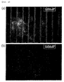
- FIG. 1 shows observation results when the conductive ink composition according to Example 1 of the present invention was coated on a PDMS substrate, which was then transferred onto a glass substrate. As shown in FIG. 1 , it can be seen that the conductive ink composition according to the present invention had excellent coatability onto the PDMS substrate and also had excellent transferability thereonto.
- FIG. 2 and FIG. 3 show observation results when a conductive ink composition according to Comparative example 1 and a conductive ink composition according to Comparative example 2 each were coated on a PDMS substrate, which was then transferred onto a glass substrate.
- the ink composition not containing tert-butyl alcohol as a main solvent had very deteriorated coatability onto a PDMS substrate and very deteriorated transferability thereto even though it contains the high boiling point solvent and the dispersion assistant solvent of the present invention.
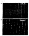
- FIG. 4 , FIG. 5 and FIG. 6 show observation results when a conductive ink composition according to Example 1, a conductive ink composition according to Example 2, and a conductive ink composition according to Example 3 each were reverse-offset printed on a glass substrate by using a PDMS material blanket.
- FIGS. 4 to 6 it can be seen that fine line patterns having a line width of about 10 ⁇ m were printed in a very uniform line width, and it can be confirmed that ink residues do not remain on a surface of the blanket after printing and the PDMS blanket had a smooth surface without swelling thereof.
- FIG. 7 shows observation results when a conductive ink composition according to Comparative example 3 was reverse-offset printed on a glass substrate by using a PDMS material blanket.
- FIG. 7 it can be confirmed that, in the case of the conductive ink composition of Comparative example 3 where the high boiling point solvent was not used, since the waiting time after the time when it is coated on the blanket and before the time when it is transferred onto the glass substrate was very short, all the ink on the blanket was not transferred onto the glass substrate but remained on the surface of he blanket. Further, it can be confirmed that it is difficult to print patterns in a line type and the printed patterns had very irregular line widths.
- Table 1 shows test results after offset-printing each of the conductive inks prepared from Examples 1 to 3 and Comparative examples 1 to 4 on a glass substrate by using a PDMS material blanket, and performing heat treatment on the glass substrate, on which the conductive ink patterns were transferred, at 350°C in the nitrogen atmosphere for 5 minutes, in the similar manner to FIGS. 4 to 7 .
- dispersion stability was evaluated by leaving an ink for 2 weeks without stirring and then taking an upper portion of the ink, followed by analysis with a thermogravimetric analyzer. Dispersion stability in the case where the metal content in the ink was reduced to 1% or less was marked as "good", and dispersion stability in the case where the metal content in the ink was reduced to 1% or more "failed".
- the binding strength to the glass was expressed by a ratio at which the metal come off from the tape by the Cross-Cut Test (ASTM D3359) after the ink transferred onto the glass substrate was fired at 350°C. A case in which the metal never come off from the tape is marked by "100” and a case in which all the metal come off from the tape is marked by "0".
- the waiting time means the time for while stable transferring is possible after coating onto the blanket.
Landscapes
- Chemical & Material Sciences (AREA)
- Engineering & Computer Science (AREA)
- Organic Chemistry (AREA)
- Wood Science & Technology (AREA)
- Materials Engineering (AREA)
- Life Sciences & Earth Sciences (AREA)
- Chemical Kinetics & Catalysis (AREA)
- Microelectronics & Electronic Packaging (AREA)
- General Chemical & Material Sciences (AREA)
- Dispersion Chemistry (AREA)
- Manufacturing & Machinery (AREA)
- Nanotechnology (AREA)
- Mechanical Engineering (AREA)
- Spectroscopy & Molecular Physics (AREA)
- Physics & Mathematics (AREA)
- Inks, Pencil-Leads, Or Crayons (AREA)
- Conductive Materials (AREA)
Abstract
Description
- The following disclosure relates to a conductive ink composition for offset or reverse-offset printing.
- As electronic devices, information terminal devices, and the like have a smaller size and a smaller weight, electronic components used in the devices tend to be gradually smaller. Therefore, sizes of wiring patterns for being mounted in the electronic components are also gradually decreased, and widths of the wiring patterns or distances between the wiring patterns are gradually decreased.
- An optical patterning method based on an exposing process and an etching process has been mainly used in order to form high-definition wiring patterns in the electronic component. However, the optical patterning method is not efficient since it unnecessarily wastes a lot of materials, requires a multistep process, and needs complicated processes such as using photoresist, developing liquids, or etching solution, and the like. Moreover, since a large-area mask needs to be used in the optical patterning method, it is difficult to apply a new design to a production line in the least amount of time. Therefore, in order to overcome disadvantages of the optical patterning method, there was developed a method of forming metal wirings through printing using an ink so that patterns are formed directly on the substrate without a mask.
- An offset printer used in forming the metal wirings consists of an ink supply part, a columnar blanket and a printing plate. The ink patterns are transferred onto a substrate to be printed by the columnar blanket.
- However, due to the trend of small sizes and high integration of products, degradation in transfer precision, such as enlargement in the line width of an ink pattern due to swelling of the blanket and the like, have emerged as serious problems. Hence, it is urgent to develop a conductive ink composition capable of forming ultra-fine metal patterns having a very small wiring width or a distance between wiring patterns.
- An object of the present invention is to provide a conductive ink composition for offset or reverse-offset printing, capable of having excellent coatability onto a blanket, preventing swelling of the blanket, and having excellent transferability onto substrates to be printed including glass, and a conductive ink composition capable of having excellent dispersion stability, forming metal wirings having ultrafine patterns, and having excellent resistivity.
- Hereinafter, an ink composition of the present invention will be described in detail. Here, unless indicated otherwise, the terms used in the specification including technical and scientific terms have the same meaning as those that are usually understood by those who skilled in the art to which the present invention pertains, and detailed description of the known functions and constitutions that may obscure the gist of the present invention will be omitted.
- A conductive ink composition according to the present invention is characterized by being an ink composition for offset or reverse-offset printing, and contains a high boiling point solvent having a boiling point of 180 to 250°C and a dispersion assistant solvent having a boiling point of 50 to 150°C, together with metal particles and tert-butyl alcohol, which is a main solvent.
- In the conductive ink composition according to an embodiment of the present invention, the dispersion assistant solvent may have a solubility parameter of 9 to 11.
- The conductive ink composition according to an embodiment of the present invention may contain tert-butyl alcohol as a main solvent, together with metal particles for giving conductivity thereto. The tert-butyl alcohol may be contained in a content of 40 to 65 wt% based on the total weight of the ink composition.
- The tert-butyl alcohol constitutes a medium of the ink composition together with the high boiling point solvent and the dispersion assistant solvent, which will be described later, and thus, provides excellent coatability onto a material of the blanket and prevents swelling of the blanket.
- The conductive ink composition of the present invention can have excellent coatability onto a polydimethylsiloxane (PDMS) material blanket and can prevent swelling of the PDMS material blanket.
- In the case where other organic solvents having a similar solubility parameter (hereinafter, SP) to tert-butyl alcohol (SP: 10.6) is used as a main solvent, a conductive ink composition may not exhibit sufficient coatability and transferability onto the material of the blanket even though it contains the high boiling point solvent and the dispersion assistant solvent according to the present invention.
- For example, in the case where solvents, such as isobutanol (SP: 10.5), sec-butanol (SP: 10.8), ethoxy ethanol (SP: 10.5), isopropyl alcohol (SP: 11.5), and propylene glycol monomethyl ether acetate (SP: 9.2), are used as the main solvent, coatability of the conductive ink composition may be severely deteriorated. In the case where solvents having a low SP, such as toluene (SP: 8.9) and isopropyl acetate (SP: 8.4) are used as a main solvent, coatability is excellent but swelling of the blanket is worse.
- In the conductive ink composition according to an embodiment of the present invention, the t-butyl alcohol may be contained in a content of 40 to 65 wt%, preferably 40 to 60 wt%, and more preferably 40 to 50 wt% based on the total weight of the ink composition. If the content of the t-butyl alcohol is below 40 wt%, coatability of the conductive ink composition may be at risk of deterioration. Further, if above 65 wt%, electric properties of conductive patterns to be printed may be at risk of deterioration.
- As such, the conductive ink composition according to the present invention employs tert-butyl alcohol as a main solvent, and a high boiling point solvent having a boiling point of 180 to 250°C and a dispersion assistant solvent having a boiling point of 50 to 150°C, as a sub solvent, and thus, can obtain excellent coatability and transferability, prevent swelling of a material of the blanket, and secure the waiting time of 30 seconds or longer after coating and before transferring. Further, the conductive ink composition according to the present invention is characterized by forming a uniform coating surface, preventing pinholes, improving dispersibility thereof, and preventing nozzles from being blocked.
- For a substantial example, the high boiling point solvent may be at least one selected from terpineol, ethyl carbitol acetate, and butyl carbitol acetate.
- The conductive ink composition according to an embodiment of the present invention may contain the high boiling point solvent in a content of 3 to 15 wt%, preferably 3 to 10 wt%, and more preferably 5 to 10 wt%.
- The conductive ink composition according to an embodiment of the present invention contains the high boiling point solvent having a boiling point of 180 to 250°C in a content of 3 to 15 wt% based on the total weight of the ink composition while employing tert-butyl alcohol as the main solvent, and thus, can secure the waiting time of 30 seconds or longer after coating and before transferring, can form a uniform coating surface by preventing agglomeration of the high boiling point solvent, and prevent pinholes.
- In the conductive ink composition according to an embodiment of the present invention, the dispersion assistant solvent may have a boiling point of 50 to 150°C and a solubility parameter of 9 to 11. For a substantial example, the dispersion assistant solvent may be at least one selected from acetone and propylene glycol monomethyl ether acetate.
- The conductive ink composition according to an embodiment of the present invention may contain the dispersion assistant solvent in a content of 10 to 30 wt%, preferably 10 to 20 wt%, and more preferably 15 to 20 wt%.
- As such, the conductive ink composition according to an embodiment of the present invention contains a dispersion assistant solvent having a boiling point of 50 to 150°C and a solubility parameter of preferably 9 to 11, in a content of 10 to 30 wt% based on the total weight of the ink composition while employing tert-butyl alcohol as a main solvent, and thus, can prevent swelling of PDMS, improve dispersibility thereof, prevent nozzles from being blocked by controlling volatile characteristics, and form a uniform coating surface.
- The conductive ink composition according to an embodiment of the present invention employs the metal particles for giving conductivity thereto, and the metal particles may be copper particles, silver particles, or a mixture particles thereof, having an average particle size of 5nm to 100nm. The metal particles may include metal particles prepared by a liquid phase reduction method.
- The conductive ink composition according to an embodiment of the present invention may contain the metal particles in a content of 20 to 40 wt%, preferably 20 to 35 wt%, and more preferably 25 to 35 wt%, based on the total weight of the ink composition.
- The conductive ink composition according to an embodiment of the present invention may contain the metal particles in a content of 20 to 40 wt% based on the total weight of the ink composition. When the ink composition contains the metal particles of 20 to 40 wt%, a film thickness after coating and transferring is about 200nm or thicker, so that excellent electric conductivity can be obtained after firing, and here, the film thickness is maintained to be 500nm or thinner, so that very thin fine conductive patterns can be formed.
- The conductive ink composition according to an embodiment of the present invention may further contain a binder and a dispersant.
- In the conductive ink composition according to an embodiment of the present invention, the binder enhances binding strength between sintered ink patterns and a substrate on which the ink patterns are located. A binder resin that is commonly used in a field of ink composition easily dissolved in the above-described medium may be used for the binder. For example, the binder may be at least one material selected from phenol based resins and acrylic based resins. The acrylic based resins may include polyacrylic acid resin or polyacrylic ester resin, and the phenol based resins may include alkyl phenol based resins. The alkyl phenol based resins may include alkyl phenol-formaldehyde resin.
- In the conductive ink composition according to an embodiment of the present invention, the binder may be contained in a content of 0.3 to 2 wt% and preferably 0.5 to 1.5 wt% based on the total weight of the ink composition, in order to obtain sufficient binding strength and prevent a deterioration in densification between the metal particles at the time of sintering.
- In the conductive ink composition according to an embodiment of the present invention, the dispersant for improving dispersion stability may be a copolymer having an acid value of 50mg KOH/g or higher and an amine value of 100mg KOH/g or lower. For example, the dispersant may be a copolymer having an acid value of 50mg KOH/g to 200mg KOH/g and an amine value of 0mg KOH/g to 100mg KOH/g. For a substantial example, BYK102 (acid value: 101mg KOH/g, amine value: 0mg KOH/g), BYK110 (acid value: 53mg KOH/g, amine value: 0mg KOH/g), BYK145 (acid value: 76mg KOH/g, amine value: 71mg KOH/g), BYK180 (acid value: 94mg KOH/g, amine value: 94mg KOH/g), BYK995 (acid value: 53mg KOH/g, amine value: 0mg KOH/g), and BYK996 (acid value: 71mg KOH/g, amine value: 0mg KOH/g), which are commercial products from BYK Chemie Company, satisfying the above acid values and amine values, may be used as the dispersant.
- The conductive ink composition according to an embodiment of the present invention may contain the dispersant in a content of 1 to 5 wt%, and preferably 1 to 3 wt% based on the total weight of the ink composition.
- According to the conductive ink composition according to an embodiment of the present invention, conductive ink patterns may be printed as a target substrate by the PDMS material blanket. In addition, an electrode for a transistor, such as, a liquid crystal display thin film transistor (LCD TFT) or an organic field-effect transistor (OTFT), or a solar cell can be effectively formed by using the conductive ink composition according to an embodiment of the present invention. Here, the electrode for a solar cell may include a front electrode, a rear electrode, or a bus bar electrode for the solar cell.
- The conductive ink composition according to the present invention can have excellent coatability onto a material of the blanket, particularly, a material of the PDMS blanket, and excellent stability onto the material of the blanket, thereby preventing swelling of the blanket. Further, conductive ink composition according to the present invention can obtain excellent transferability, secure the waiting time of 30 seconds or longer, form ultrafine metal patterns having a uniform coating surface and high electric conductivity, prevent pinholes, obtain excellent dispersion stability, and prevent nozzles from being blocked.
-
-
FIG. 1 shows optical pictures of coating ((a) ofFIG. 1 ) and transferring ((b) ofFIG. 1 ) results using an ink composition according to Example 1 of the present invention; -
FIG. 2 shows optical pictures of coating ((a) ofFIG. 2 ) and transferring ((b) ofFIG. 2 ) results using an ink composition according to Comparative example 1 of the present invention; -
FIG. 3 shows optical pictures of coating ((a) ofFIG. 3 ) and transferring ((b) ofFIG. 3 ) results using an ink composition according to Comparative example 2 of the present invention; -
FIG. 4 shows pictures obtained by observing a surface of a glass substrate ((a) ofFIG. 4 ) and a surface of a blanket ((b) ofFIG. 4 ) after transferring, in pattern transferring results using the ink composition according to Example 1 of the present invention; -
FIG. 5 shows pictures obtained by observing a surface of a glass substrate ((a) ofFIG. 5 ) and a surface of a blanket ((b) ofFIG. 5 ) after transferring, in pattern transferring results using the ink composition according to Example 2 of the present invention; -
FIG. 6 shows pictures obtained by observing a surface of a glass substrate ((a) ofFIG. 6 ) and a surface of a blanket ((b) ofFIG. 6 ) after transferring, in pattern transferring results using the ink composition according to Example 3 of the present invention; and -
FIG. 7 shows pictures obtained by observing a surface of a glass substrate ((a) ofFIG. 7 ) and a surface of a blanket ((b) ofFIG. 7 ) after transferring, in pattern transferring results using the ink composition according to Comparative example 3. - 30 wt% of copper metal particles having an average particle size of 20nm, 47 wt% of tert-butyl alcohol as a main solvent, 5 wt% of terpineol as a high boiling point solvent, 15 wt% of propylene glycol monomethyl ether acetate as a dispersion assistant solvent, 1 wt% of polyacrylic acid resin (Aldrich, Mw: 1800 or less) as a binder, and 2 wt% of BYK180 (copolymer having an acid value of 94mg KOH/g and an amine value of 94 mg KOH/g) as a dispersant were mixed, and then the mixture was milled by using a boll mill for 2 hours. The thus obtained material was used as an ink for printing.
- 30 wt% of copper metal particles having an average particle size of 20nm, 42 wt% of tert-butyl alcohol as a main solvent, 10 wt% of terpineol as a high boiling point solvent, 15 wt% of propylene glycol monomethyl ether acetate as a dispersion assistant solvent, 1wt% of polyacrylic acid resin (Aldrich, Mw: 1800 or less) as a binder, and 2 wt% of BYK180 (copolymer having an acid value of 94mg KOH/g and an amine value of 94 mg KOH/g) as a dispersant were mixed, and then the mixture was milled by using a boll mill for 2 hours. The thus obtained material was used as an ink for printing.
- 30 wt% of copper metal particles having an average particle size of 20nm, 47 wt% of tert-butyl alcohol as a main solvent, 5 wt% of terpineol as a high boiling point solvent, 15wt% of acetone as a dispersion assistant solvent, 1 wt% of alkyl phenol-formaldehyde resin (Tackirol-101) as a binder, and 2 wt% of BYK110 (copolymer having an acid value of 53 mg KOH/g and an amine value of 0 mg KOH/g) as a dispersant were mixed, and then the mixture was milled by using a boll mill for 2 hours. The thus obtained material was used as an ink for printing.
- An ink for printing was prepared by the same method as Example 1 except that toluene was used as a main solvent.
- An ink for printing was prepared by the same method as Example 1 except that ethanol was used as a main solvent.
- 30 wt% of copper metal particles having an average particle size of 20nm, 52 wt% of tert-butyl alcohol as a main solvent, 15 wt% of propylene glycol monomethyl ether acetate as a dispersion assistant solvent, 1wt% of polyacrylic acid resin (Aldrich, Mw: 1800 or less) as a binder, and 2 wt% of BYK110 (copolymer having an acid value of 53 mg KOH/g and an amine value of 0 mg KOH/g) as a dispersant were mixed without using a high boiling point solvent, and then the mixture was milled by using a boll mill for 2 hours. The thus obtained material was used as an ink for printing.
- 30 wt% of copper metal particles having an average particle size of 20nm, 62 wt% of tert-butyl alcohol as a main solvent, 5 wt% of terpineol as a high boiling point solvent, 1 wt% of polyacrylic acid resin (Aldrich, Mw: 1800 or less) as a binder, and 2 wt% of BYK110 (copolymer having an acid value of 53 mg KOH/g and an amine value of 0 mg KOH/g) as a dispersant were mixed without using a dispersant assistant solvent, and then the mixture was milled by using a boll mill for 2 hours. The thus obtained material was used as an ink for printing.
-
FIG. 1 shows observation results when the conductive ink composition according to Example 1 of the present invention was coated on a PDMS substrate, which was then transferred onto a glass substrate. As shown inFIG. 1 , it can be seen that the conductive ink composition according to the present invention had excellent coatability onto the PDMS substrate and also had excellent transferability thereonto. -
FIG. 2 andFIG. 3 show observation results when a conductive ink composition according to Comparative example 1 and a conductive ink composition according to Comparative example 2 each were coated on a PDMS substrate, which was then transferred onto a glass substrate. As shown inFIGS. 2 and3 , it can be confirmed that the ink composition not containing tert-butyl alcohol as a main solvent had very deteriorated coatability onto a PDMS substrate and very deteriorated transferability thereto even though it contains the high boiling point solvent and the dispersion assistant solvent of the present invention. -
FIG. 4 ,FIG. 5 andFIG. 6 show observation results when a conductive ink composition according to Example 1, a conductive ink composition according to Example 2, and a conductive ink composition according to Example 3 each were reverse-offset printed on a glass substrate by using a PDMS material blanket. As shown inFIGS. 4 to 6 , it can be seen that fine line patterns having a line width of about 10µm were printed in a very uniform line width, and it can be confirmed that ink residues do not remain on a surface of the blanket after printing and the PDMS blanket had a smooth surface without swelling thereof. -
FIG. 7 shows observation results when a conductive ink composition according to Comparative example 3 was reverse-offset printed on a glass substrate by using a PDMS material blanket. As shown inFIG. 7 , it can be confirmed that, in the case of the conductive ink composition of Comparative example 3 where the high boiling point solvent was not used, since the waiting time after the time when it is coated on the blanket and before the time when it is transferred onto the glass substrate was very short, all the ink on the blanket was not transferred onto the glass substrate but remained on the surface of he blanket. Further, it can be confirmed that it is difficult to print patterns in a line type and the printed patterns had very irregular line widths. - Table 1 shows test results after offset-printing each of the conductive inks prepared from Examples 1 to 3 and Comparative examples 1 to 4 on a glass substrate by using a PDMS material blanket, and performing heat treatment on the glass substrate, on which the conductive ink patterns were transferred, at 350°C in the nitrogen atmosphere for 5 minutes, in the similar manner to
FIGS. 4 to 7 .[Table 1] Ink Coatability Transferability swelling of blanket Dispersion stability binding strength to glass waiting time resistivity example 1 good good weak good 100 70 4.7 example 2 good good weak good 100 100 4.2 example 3 good good weak good 100 50 4.5 Comparative example 1 good failed strong good 100 10 - Comparative example 2 failed failed weak failed 100 - - comparative example 3 good good weak good 100 10 4.9 comparative example 4 good good weak failed 100 100 5.1 - In Table 1, coatability in the case where uniform coating was performed without generation of pinholes was marked as "good" and coatability in the case where pinholes were generated was marked as "failed", and transferability in the case where stable transferring was performed onto the glass substrate after the waiting time of 30 seconds, was marked as "good" and transferability in the case where stable transferring was not performed, such as, a pattern was disconnected or a line width of the pattern became thinner than the original line widths thereof was marked as "failed".
- In addition, dispersion stability was evaluated by leaving an ink for 2 weeks without stirring and then taking an upper portion of the ink, followed by analysis with a thermogravimetric analyzer. Dispersion stability in the case where the metal content in the ink was reduced to 1% or less was marked as "good", and dispersion stability in the case where the metal content in the ink was reduced to 1% or more "failed".
- The binding strength to the glass was expressed by a ratio at which the metal come off from the tape by the Cross-Cut Test (ASTM D3359) after the ink transferred onto the glass substrate was fired at 350°C. A case in which the metal never come off from the tape is marked by "100" and a case in which all the metal come off from the tape is marked by "0". The waiting time means the time for while stable transferring is possible after coating onto the blanket.
- As described above, although the present invention is described by specific matters such as concrete components and the like, exemplary embodiments, and drawings, they are provided only for assisting in the entire understanding of the present invention. Therefore, the present invention is not limited to the exemplary embodiments. Various modifications and changes may be made by those skilled in the art to which the present invention pertains from this description. Therefore, the spirit of the present invention should not be limited to the above-described exemplary embodiments and the following claims as well as all modified equally or equivalently to the claims are intended to fall within the scopes and spirit of the invention.
Claims (11)
- A conductive ink composition for offset or reverse-offset printing, the conductive ink composition comprising a high boiling point solvent having a boiling point of 180 to 250°C and a dispersion assistant solvent having a boiling point of 50 to 150°C, together with metal particles and tert-butyl alcohol as a main solvent.
- The conductive ink composition of claim 1, wherein the dispersion assistant solvent has a solubility parameter of 9 to 11.
- The conductive ink composition of claim 1, wherein it is printed by a polydimethylsiloxane (PDMS) material blanket.
- The conductive ink composition of claim 1, wherein the high boiling point solvent is at least one selected from terpineol, ethyl carbitol acetate, and butyl carbitol acetate.
- The conductive ink composition of claim 1, wherein the dispersion assistant solvent is at least one selected from acetone and propylene glycol monomethyl ether acetate.
- The conductive ink composition of claim 1, wherein the metal particles are contained in a content of 20 to 40 wt%; the main solvent 40 to 65 wt%; the high boiling point solvent 3 to 15 wt%; and the dispersion assistant solvent 10 to 30 wt%.
- The conductive ink composition of claim 1, wherein the metal particles are copper particles, silver particles, or mixed particles thereof, having an average particle size of 5nm to 100nm.
- The conductive ink composition of claim 1, further comprising a binder and a dispersant.
- The conductive ink composition of claim 8, wherein the binder is at least one selected from phenol based resin and acrylic based resin.
- The conductive ink composition of claim 8, wherein the dispersant is a copolymer having an acid value of 50mg KOH/g or higher and an amine value of 100mg KOH/g or lower.
- The conductive ink composition of claim 8, wherein the binder is contained in a content of 0.3 to 2 wt%; and the dispersant 1 to 5 wt%.
Applications Claiming Priority (3)
| Application Number | Priority Date | Filing Date | Title |
|---|---|---|---|
| KR20110017016 | 2011-02-25 | ||
| KR1020120018482A KR101260956B1 (en) | 2011-02-25 | 2012-02-23 | Composition of Conductive Ink for Offset or Reverseoffset Printing |
| PCT/KR2012/001411 WO2012115475A2 (en) | 2011-02-25 | 2012-02-24 | Conductive ink composition for offset or reverse-offset printing |
Publications (3)
| Publication Number | Publication Date |
|---|---|
| EP2679639A2 true EP2679639A2 (en) | 2014-01-01 |
| EP2679639A4 EP2679639A4 (en) | 2015-09-23 |
| EP2679639B1 EP2679639B1 (en) | 2016-10-19 |
Family
ID=47109466
Family Applications (1)
| Application Number | Title | Priority Date | Filing Date |
|---|---|---|---|
| EP12749676.8A Active EP2679639B1 (en) | 2011-02-25 | 2012-02-24 | Conductive ink composition for offset or reverse-offset printing |
Country Status (6)
| Country | Link |
|---|---|
| US (2) | US20140008586A1 (en) |
| EP (1) | EP2679639B1 (en) |
| JP (1) | JP5671157B2 (en) |
| KR (1) | KR101260956B1 (en) |
| TW (1) | TWI496169B (en) |
| WO (1) | WO2012115475A2 (en) |
Cited By (1)
| Publication number | Priority date | Publication date | Assignee | Title |
|---|---|---|---|---|
| WO2021115750A1 (en) * | 2019-12-11 | 2021-06-17 | Genes'ink | Ink based on silver nanoparticles |
Families Citing this family (19)
| Publication number | Priority date | Publication date | Assignee | Title |
|---|---|---|---|---|
| CN103562326B (en) * | 2011-04-05 | 2016-01-20 | Lg化学株式会社 | For the composition that prints and the printing process using said composition |
| KR101356831B1 (en) * | 2011-04-05 | 2014-02-06 | 주식회사 엘지화학 | Composition for printing and printing method using the same |
| FR3008103B1 (en) | 2013-07-03 | 2015-09-11 | Genes Ink Sas | INK COMPOSITION BASED ON NANOPARTICLES |
| JP6175500B2 (en) * | 2013-07-23 | 2017-08-02 | 旭化成株式会社 | Copper and / or copper oxide dispersion, and conductive film formed using the dispersion |
| JP6143698B2 (en) * | 2014-03-28 | 2017-06-07 | 富士フイルム株式会社 | Wiring pattern forming method, organic transistor manufacturing method, and organic transistor |
| JP6016842B2 (en) * | 2014-03-31 | 2016-10-26 | 富士フイルム株式会社 | Method for producing conductive film and composition for forming conductive film |
| JP6532862B2 (en) * | 2014-04-01 | 2019-06-19 | 株式会社ダイセル | Silver nanoparticle-containing ink for intaglio offset printing and method for producing the same |
| TWI574284B (en) * | 2014-06-25 | 2017-03-11 | 柯尼卡美能達股份有限公司 | Method of manufacturing conductive patterned substrate |
| KR101789862B1 (en) | 2014-10-07 | 2017-10-25 | 주식회사 엘지화학 | Composition for printing and printing method using the same |
| KR102056972B1 (en) * | 2014-11-25 | 2019-12-17 | 반도 카가쿠 가부시키가이샤 | Conductive ink |
| JP6618969B2 (en) * | 2017-10-13 | 2019-12-11 | 株式会社ノリタケカンパニーリミテド | Conductive paste |
| JP7276140B2 (en) * | 2017-11-14 | 2023-05-18 | 株式会社レゾナック | COMPOSITION, CONDUCTOR AND MANUFACTURING METHOD THEREOF, AND STRUCTURE |
| EP3530706B1 (en) | 2018-02-27 | 2022-12-07 | Fundación I + D Automoción y Mecatrónica | Method for producing a conductive ink for offset printing and conductive ink thus produced |
| WO2019216756A1 (en) * | 2018-05-08 | 2019-11-14 | Jabil, Inc. | Stretchable conductive ink package based on dual-system polysiloxane |
| KR102501588B1 (en) * | 2018-08-08 | 2023-02-21 | 미쓰이금속광업주식회사 | Composition for bonding, bonding structure of conductors and manufacturing method thereof |
| JP2024029655A (en) * | 2022-08-22 | 2024-03-06 | 株式会社日本触媒 | Dispersion containing inorganic particles |
| JP2026002682A (en) * | 2024-06-21 | 2026-01-08 | Jx金属株式会社 | Copper ink, electronic circuit board, and method for manufacturing electronic circuit board |
| JP2026002684A (en) * | 2024-06-21 | 2026-01-08 | Jx金属株式会社 | Copper ink, electronic circuit board, and method for manufacturing electronic circuit board |
| JP2026002683A (en) * | 2024-06-21 | 2026-01-08 | Jx金属株式会社 | Copper ink, electronic circuit board, and method for manufacturing electronic circuit board |
Family Cites Families (15)
| Publication number | Priority date | Publication date | Assignee | Title |
|---|---|---|---|---|
| JP3102269B2 (en) * | 1994-06-23 | 2000-10-23 | ブラザー工業株式会社 | Inkjet recording method |
| JP3113850B2 (en) | 1997-11-28 | 2000-12-04 | 日本写真印刷株式会社 | Ink for forming transparent conductive film |
| WO2003106573A1 (en) * | 2002-06-13 | 2003-12-24 | Nanopowders Industries Ltd. | A method for the production of conductive and transparent nano-coatings and nano-inks and nano-powder coatings and inks produced thereby |
| US7062848B2 (en) * | 2003-09-18 | 2006-06-20 | Hewlett-Packard Development Company, L.P. | Printable compositions having anisometric nanostructures for use in printed electronics |
| JP4828791B2 (en) * | 2003-10-24 | 2011-11-30 | 光村印刷株式会社 | Ink composition for precision patterning |
| KR100667958B1 (en) * | 2005-04-14 | 2007-01-11 | 주식회사 잉크테크 | Silver ink composition |
| CN101137730B (en) * | 2005-03-11 | 2011-11-16 | 东洋油墨制造株式会社 | Electrically conductive ink, electrically conductive circuit, and noncontact-type medium |
| TWI326297B (en) * | 2005-03-21 | 2010-06-21 | Inktec Co Ltd | Conductive ink composition and preparing method thereof |
| JP2007272181A (en) * | 2006-03-06 | 2007-10-18 | Dainippon Printing Co Ltd | Manufacturing method of color filter |
| US8241528B2 (en) * | 2007-03-15 | 2012-08-14 | Dic Corporation | Conductive ink for letterpress reverse printing |
| KR20080088712A (en) * | 2007-03-30 | 2008-10-06 | 삼성전자주식회사 | Conductive ink composition and method of forming conductive pattern using same |
| US10231344B2 (en) * | 2007-05-18 | 2019-03-12 | Applied Nanotech Holdings, Inc. | Metallic ink |
| JP5255792B2 (en) * | 2007-07-18 | 2013-08-07 | 太陽ホールディングス株式会社 | Conductive paste composition, translucent conductive film using the composition, and method for producing the same |
| JP2009062524A (en) * | 2007-08-09 | 2009-03-26 | Mitsubishi Materials Corp | Conductive ink for offset printing and method for producing electrode substrate for plasma display panel using the conductive ink |
| CN102308367B (en) * | 2009-02-06 | 2015-06-10 | Lg化学株式会社 | Method for manufacturing insulated conductive pattern and laminate |
-
2012
- 2012-02-23 KR KR1020120018482A patent/KR101260956B1/en active Active
- 2012-02-24 TW TW101106192A patent/TWI496169B/en not_active IP Right Cessation
- 2012-02-24 JP JP2013547370A patent/JP5671157B2/en active Active
- 2012-02-24 WO PCT/KR2012/001411 patent/WO2012115475A2/en not_active Ceased
- 2012-02-24 EP EP12749676.8A patent/EP2679639B1/en active Active
- 2012-02-24 US US13/976,572 patent/US20140008586A1/en not_active Abandoned
-
2016
- 2016-04-28 US US15/141,186 patent/US20160249460A1/en not_active Abandoned
Cited By (3)
| Publication number | Priority date | Publication date | Assignee | Title |
|---|---|---|---|---|
| WO2021115750A1 (en) * | 2019-12-11 | 2021-06-17 | Genes'ink | Ink based on silver nanoparticles |
| FR3104600A1 (en) * | 2019-12-11 | 2021-06-18 | Genes'ink Sa | Ink based on silver nanoparticles |
| CN114846093A (en) * | 2019-12-11 | 2022-08-02 | 吉尼斯油墨公司 | Ink based on silver nanoparticles |
Also Published As
| Publication number | Publication date |
|---|---|
| KR101260956B1 (en) | 2013-05-06 |
| EP2679639A4 (en) | 2015-09-23 |
| US20160249460A1 (en) | 2016-08-25 |
| US20140008586A1 (en) | 2014-01-09 |
| EP2679639B1 (en) | 2016-10-19 |
| TWI496169B (en) | 2015-08-11 |
| JP2014507510A (en) | 2014-03-27 |
| WO2012115475A3 (en) | 2012-12-20 |
| KR20120098456A (en) | 2012-09-05 |
| TW201239899A (en) | 2012-10-01 |
| JP5671157B2 (en) | 2015-02-18 |
| WO2012115475A2 (en) | 2012-08-30 |
Similar Documents
| Publication | Publication Date | Title |
|---|---|---|
| EP2679639B1 (en) | Conductive ink composition for offset or reverse-offset printing | |
| CN101632136B (en) | Conductive ink for letterpress reverse printing | |
| EP3305853B1 (en) | Dispersion | |
| US7806974B2 (en) | Highly conductive ink composition and method for fabricating a metal conductive pattern | |
| EP3026677B1 (en) | Copper and/or copper oxide dispersion, and method for electroconductive film using dispersion | |
| KR101700615B1 (en) | Method for preparing matal nano-particles, matal nano-particles prepared therefrom and metal ink composition comprising same | |
| TWI622998B (en) | Conductive composition and hardened product using the same | |
| JP5701379B2 (en) | Conductive metal ink composition and method for forming conductive pattern | |
| US9972413B2 (en) | Metal particle dispersion for electroconductive substrates, method for producing the same, and method for producing an electroconductive substrate | |
| US8507104B2 (en) | Metal coating, forming method thereof, and metal wiring | |
| CN102510783A (en) | Low-temperature sinterable silver nanoparticle composition and electronic component formed using that composition | |
| US20160200931A1 (en) | Nanosilver Ink Compositions Comprising Polystyrene Additives | |
| DE102016225051A1 (en) | INTERMEDIATE COMPOSITION FOR ELECTRONIC PRINTING | |
| WO2013073331A1 (en) | Method for forming copper film, copper film, circuit substrate, and copper-film-forming composition solution | |
| US9953740B2 (en) | Dispersant, metal particle dispersion for electroconductive substrates, and method for producing electroconductive substrate | |
| CN104170021B (en) | Conductive composition and circuit substrate with conductive film formed therefrom | |
| KR101081320B1 (en) | Conductive paste composition | |
| KR101351699B1 (en) | Conductive paste composition, electrode including the same and fabrication method of the electrode | |
| KR20120028126A (en) | Method for producing conductive coating film, and primer composition therefor | |
| KR20160007025A (en) | Ink composition for reverse offset printing and reverse offset printing method using the same | |
| JP6111587B2 (en) | Method for manufacturing conductive substrate |
Legal Events
| Date | Code | Title | Description |
|---|---|---|---|
| PUAI | Public reference made under article 153(3) epc to a published international application that has entered the european phase |
Free format text: ORIGINAL CODE: 0009012 |
|
| 17P | Request for examination filed |
Effective date: 20130625 |
|
| AK | Designated contracting states |
Kind code of ref document: A2 Designated state(s): AL AT BE BG CH CY CZ DE DK EE ES FI FR GB GR HR HU IE IS IT LI LT LU LV MC MK MT NL NO PL PT RO RS SE SI SK SM TR |
|
| DAX | Request for extension of the european patent (deleted) | ||
| A4 | Supplementary search report drawn up and despatched |
Effective date: 20150826 |
|
| RIC1 | Information provided on ipc code assigned before grant |
Ipc: B41M 1/00 20060101ALI20150820BHEP Ipc: H01B 1/22 20060101ALI20150820BHEP Ipc: C09D 1/02 20060101ALI20150820BHEP Ipc: C09D 1/00 20060101AFI20150820BHEP |
|
| GRAP | Despatch of communication of intention to grant a patent |
Free format text: ORIGINAL CODE: EPIDOSNIGR1 |
|
| INTG | Intention to grant announced |
Effective date: 20160511 |
|
| RIN1 | Information on inventor provided before grant (corrected) |
Inventor name: PAIK, CHOONG-HOON Inventor name: SON, WON II Inventor name: OH, SEOK-HEON Inventor name: KIM, EUI DUK |
|
| GRAS | Grant fee paid |
Free format text: ORIGINAL CODE: EPIDOSNIGR3 |
|
| GRAA | (expected) grant |
Free format text: ORIGINAL CODE: 0009210 |
|
| AK | Designated contracting states |
Kind code of ref document: B1 Designated state(s): AL AT BE BG CH CY CZ DE DK EE ES FI FR GB GR HR HU IE IS IT LI LT LU LV MC MK MT NL NO PL PT RO RS SE SI SK SM TR |
|
| REG | Reference to a national code |
Ref country code: GB Ref legal event code: FG4D |
|
| REG | Reference to a national code |
Ref country code: CH Ref legal event code: EP |
|
| REG | Reference to a national code |
Ref country code: AT Ref legal event code: REF Ref document number: 838321 Country of ref document: AT Kind code of ref document: T Effective date: 20161115 |
|
| REG | Reference to a national code |
Ref country code: IE Ref legal event code: FG4D |
|
| REG | Reference to a national code |
Ref country code: DE Ref legal event code: R096 Ref document number: 602012024346 Country of ref document: DE |
|
| REG | Reference to a national code |
Ref country code: NL Ref legal event code: MP Effective date: 20161019 |
|
| REG | Reference to a national code |
Ref country code: LT Ref legal event code: MG4D |
|
| PG25 | Lapsed in a contracting state [announced via postgrant information from national office to epo] |
Ref country code: LV Free format text: LAPSE BECAUSE OF FAILURE TO SUBMIT A TRANSLATION OF THE DESCRIPTION OR TO PAY THE FEE WITHIN THE PRESCRIBED TIME-LIMIT Effective date: 20161019 |
|
| REG | Reference to a national code |
Ref country code: AT Ref legal event code: MK05 Ref document number: 838321 Country of ref document: AT Kind code of ref document: T Effective date: 20161019 |
|
| PG25 | Lapsed in a contracting state [announced via postgrant information from national office to epo] |
Ref country code: NO Free format text: LAPSE BECAUSE OF FAILURE TO SUBMIT A TRANSLATION OF THE DESCRIPTION OR TO PAY THE FEE WITHIN THE PRESCRIBED TIME-LIMIT Effective date: 20170119 Ref country code: SE Free format text: LAPSE BECAUSE OF FAILURE TO SUBMIT A TRANSLATION OF THE DESCRIPTION OR TO PAY THE FEE WITHIN THE PRESCRIBED TIME-LIMIT Effective date: 20161019 Ref country code: GR Free format text: LAPSE BECAUSE OF FAILURE TO SUBMIT A TRANSLATION OF THE DESCRIPTION OR TO PAY THE FEE WITHIN THE PRESCRIBED TIME-LIMIT Effective date: 20170120 Ref country code: LT Free format text: LAPSE BECAUSE OF FAILURE TO SUBMIT A TRANSLATION OF THE DESCRIPTION OR TO PAY THE FEE WITHIN THE PRESCRIBED TIME-LIMIT Effective date: 20161019 |
|
| PG25 | Lapsed in a contracting state [announced via postgrant information from national office to epo] |
Ref country code: IS Free format text: LAPSE BECAUSE OF FAILURE TO SUBMIT A TRANSLATION OF THE DESCRIPTION OR TO PAY THE FEE WITHIN THE PRESCRIBED TIME-LIMIT Effective date: 20170219 Ref country code: NL Free format text: LAPSE BECAUSE OF FAILURE TO SUBMIT A TRANSLATION OF THE DESCRIPTION OR TO PAY THE FEE WITHIN THE PRESCRIBED TIME-LIMIT Effective date: 20161019 Ref country code: RS Free format text: LAPSE BECAUSE OF FAILURE TO SUBMIT A TRANSLATION OF THE DESCRIPTION OR TO PAY THE FEE WITHIN THE PRESCRIBED TIME-LIMIT Effective date: 20161019 Ref country code: FI Free format text: LAPSE BECAUSE OF FAILURE TO SUBMIT A TRANSLATION OF THE DESCRIPTION OR TO PAY THE FEE WITHIN THE PRESCRIBED TIME-LIMIT Effective date: 20161019 Ref country code: AT Free format text: LAPSE BECAUSE OF FAILURE TO SUBMIT A TRANSLATION OF THE DESCRIPTION OR TO PAY THE FEE WITHIN THE PRESCRIBED TIME-LIMIT Effective date: 20161019 Ref country code: PL Free format text: LAPSE BECAUSE OF FAILURE TO SUBMIT A TRANSLATION OF THE DESCRIPTION OR TO PAY THE FEE WITHIN THE PRESCRIBED TIME-LIMIT Effective date: 20161019 Ref country code: PT Free format text: LAPSE BECAUSE OF FAILURE TO SUBMIT A TRANSLATION OF THE DESCRIPTION OR TO PAY THE FEE WITHIN THE PRESCRIBED TIME-LIMIT Effective date: 20170220 Ref country code: ES Free format text: LAPSE BECAUSE OF FAILURE TO SUBMIT A TRANSLATION OF THE DESCRIPTION OR TO PAY THE FEE WITHIN THE PRESCRIBED TIME-LIMIT Effective date: 20161019 Ref country code: BE Free format text: LAPSE BECAUSE OF FAILURE TO SUBMIT A TRANSLATION OF THE DESCRIPTION OR TO PAY THE FEE WITHIN THE PRESCRIBED TIME-LIMIT Effective date: 20161019 Ref country code: HR Free format text: LAPSE BECAUSE OF FAILURE TO SUBMIT A TRANSLATION OF THE DESCRIPTION OR TO PAY THE FEE WITHIN THE PRESCRIBED TIME-LIMIT Effective date: 20161019 |
|
| REG | Reference to a national code |
Ref country code: DE Ref legal event code: R097 Ref document number: 602012024346 Country of ref document: DE |
|
| PG25 | Lapsed in a contracting state [announced via postgrant information from national office to epo] |
Ref country code: SK Free format text: LAPSE BECAUSE OF FAILURE TO SUBMIT A TRANSLATION OF THE DESCRIPTION OR TO PAY THE FEE WITHIN THE PRESCRIBED TIME-LIMIT Effective date: 20161019 Ref country code: DK Free format text: LAPSE BECAUSE OF FAILURE TO SUBMIT A TRANSLATION OF THE DESCRIPTION OR TO PAY THE FEE WITHIN THE PRESCRIBED TIME-LIMIT Effective date: 20161019 Ref country code: CZ Free format text: LAPSE BECAUSE OF FAILURE TO SUBMIT A TRANSLATION OF THE DESCRIPTION OR TO PAY THE FEE WITHIN THE PRESCRIBED TIME-LIMIT Effective date: 20161019 Ref country code: EE Free format text: LAPSE BECAUSE OF FAILURE TO SUBMIT A TRANSLATION OF THE DESCRIPTION OR TO PAY THE FEE WITHIN THE PRESCRIBED TIME-LIMIT Effective date: 20161019 Ref country code: RO Free format text: LAPSE BECAUSE OF FAILURE TO SUBMIT A TRANSLATION OF THE DESCRIPTION OR TO PAY THE FEE WITHIN THE PRESCRIBED TIME-LIMIT Effective date: 20161019 |
|
| PLBE | No opposition filed within time limit |
Free format text: ORIGINAL CODE: 0009261 |
|
| STAA | Information on the status of an ep patent application or granted ep patent |
Free format text: STATUS: NO OPPOSITION FILED WITHIN TIME LIMIT |
|
| PG25 | Lapsed in a contracting state [announced via postgrant information from national office to epo] |
Ref country code: SM Free format text: LAPSE BECAUSE OF FAILURE TO SUBMIT A TRANSLATION OF THE DESCRIPTION OR TO PAY THE FEE WITHIN THE PRESCRIBED TIME-LIMIT Effective date: 20161019 Ref country code: BG Free format text: LAPSE BECAUSE OF FAILURE TO SUBMIT A TRANSLATION OF THE DESCRIPTION OR TO PAY THE FEE WITHIN THE PRESCRIBED TIME-LIMIT Effective date: 20170119 Ref country code: IT Free format text: LAPSE BECAUSE OF FAILURE TO SUBMIT A TRANSLATION OF THE DESCRIPTION OR TO PAY THE FEE WITHIN THE PRESCRIBED TIME-LIMIT Effective date: 20161019 |
|
| 26N | No opposition filed |
Effective date: 20170720 |
|
| PG25 | Lapsed in a contracting state [announced via postgrant information from national office to epo] |
Ref country code: MC Free format text: LAPSE BECAUSE OF FAILURE TO SUBMIT A TRANSLATION OF THE DESCRIPTION OR TO PAY THE FEE WITHIN THE PRESCRIBED TIME-LIMIT Effective date: 20161019 |
|
| REG | Reference to a national code |
Ref country code: CH Ref legal event code: PL |
|
| GBPC | Gb: european patent ceased through non-payment of renewal fee |
Effective date: 20170224 |
|
| PG25 | Lapsed in a contracting state [announced via postgrant information from national office to epo] |
Ref country code: CH Free format text: LAPSE BECAUSE OF NON-PAYMENT OF DUE FEES Effective date: 20170228 Ref country code: LI Free format text: LAPSE BECAUSE OF NON-PAYMENT OF DUE FEES Effective date: 20170228 |
|
| REG | Reference to a national code |
Ref country code: IE Ref legal event code: MM4A |
|
| PG25 | Lapsed in a contracting state [announced via postgrant information from national office to epo] |
Ref country code: SI Free format text: LAPSE BECAUSE OF FAILURE TO SUBMIT A TRANSLATION OF THE DESCRIPTION OR TO PAY THE FEE WITHIN THE PRESCRIBED TIME-LIMIT Effective date: 20161019 |
|
| REG | Reference to a national code |
Ref country code: FR Ref legal event code: ST Effective date: 20171031 |
|
| PG25 | Lapsed in a contracting state [announced via postgrant information from national office to epo] |
Ref country code: LU Free format text: LAPSE BECAUSE OF NON-PAYMENT OF DUE FEES Effective date: 20170224 |
|
| PG25 | Lapsed in a contracting state [announced via postgrant information from national office to epo] |
Ref country code: FR Free format text: LAPSE BECAUSE OF NON-PAYMENT OF DUE FEES Effective date: 20170228 |
|
| PG25 | Lapsed in a contracting state [announced via postgrant information from national office to epo] |
Ref country code: GB Free format text: LAPSE BECAUSE OF NON-PAYMENT OF DUE FEES Effective date: 20170224 Ref country code: IE Free format text: LAPSE BECAUSE OF NON-PAYMENT OF DUE FEES Effective date: 20170224 |
|
| PG25 | Lapsed in a contracting state [announced via postgrant information from national office to epo] |
Ref country code: MT Free format text: LAPSE BECAUSE OF NON-PAYMENT OF DUE FEES Effective date: 20170224 |
|
| PG25 | Lapsed in a contracting state [announced via postgrant information from national office to epo] |
Ref country code: HU Free format text: LAPSE BECAUSE OF FAILURE TO SUBMIT A TRANSLATION OF THE DESCRIPTION OR TO PAY THE FEE WITHIN THE PRESCRIBED TIME-LIMIT; INVALID AB INITIO Effective date: 20120224 |
|
| PG25 | Lapsed in a contracting state [announced via postgrant information from national office to epo] |
Ref country code: CY Free format text: LAPSE BECAUSE OF NON-PAYMENT OF DUE FEES Effective date: 20161019 |
|
| PG25 | Lapsed in a contracting state [announced via postgrant information from national office to epo] |
Ref country code: MK Free format text: LAPSE BECAUSE OF FAILURE TO SUBMIT A TRANSLATION OF THE DESCRIPTION OR TO PAY THE FEE WITHIN THE PRESCRIBED TIME-LIMIT Effective date: 20161019 |
|
| PG25 | Lapsed in a contracting state [announced via postgrant information from national office to epo] |
Ref country code: TR Free format text: LAPSE BECAUSE OF FAILURE TO SUBMIT A TRANSLATION OF THE DESCRIPTION OR TO PAY THE FEE WITHIN THE PRESCRIBED TIME-LIMIT Effective date: 20161019 |
|
| PG25 | Lapsed in a contracting state [announced via postgrant information from national office to epo] |
Ref country code: AL Free format text: LAPSE BECAUSE OF FAILURE TO SUBMIT A TRANSLATION OF THE DESCRIPTION OR TO PAY THE FEE WITHIN THE PRESCRIBED TIME-LIMIT Effective date: 20161019 |
|
| P01 | Opt-out of the competence of the unified patent court (upc) registered |
Effective date: 20230608 |
|
| PGFP | Annual fee paid to national office [announced via postgrant information from national office to epo] |
Ref country code: DE Payment date: 20260102 Year of fee payment: 15 |