EP2677475B1 - Method for manufacturing long-range radio frequency identification metallic product and structure thereof - Google Patents
Method for manufacturing long-range radio frequency identification metallic product and structure thereof Download PDFInfo
- Publication number
- EP2677475B1 EP2677475B1 EP20120173184 EP12173184A EP2677475B1 EP 2677475 B1 EP2677475 B1 EP 2677475B1 EP 20120173184 EP20120173184 EP 20120173184 EP 12173184 A EP12173184 A EP 12173184A EP 2677475 B1 EP2677475 B1 EP 2677475B1
- Authority
- EP
- European Patent Office
- Prior art keywords
- metallic
- antenna
- resonance chamber
- electronic tag
- rigid clip
- Prior art date
- Legal status (The legal status is an assumption and is not a legal conclusion. Google has not performed a legal analysis and makes no representation as to the accuracy of the status listed.)
- Active
Links
- 238000000034 method Methods 0.000 title claims description 92
- 238000004519 manufacturing process Methods 0.000 title claims description 30
- 230000008569 process Effects 0.000 claims description 65
- RYGMFSIKBFXOCR-UHFFFAOYSA-N Copper Chemical compound [Cu] RYGMFSIKBFXOCR-UHFFFAOYSA-N 0.000 claims description 44
- 239000003292 glue Substances 0.000 claims description 33
- 239000011889 copper foil Substances 0.000 claims description 31
- 239000000463 material Substances 0.000 claims description 21
- 238000002360 preparation method Methods 0.000 claims description 21
- 239000000919 ceramic Substances 0.000 claims description 19
- 239000000758 substrate Substances 0.000 claims description 17
- 238000004080 punching Methods 0.000 claims description 15
- 229910052802 copper Inorganic materials 0.000 claims description 13
- 239000010949 copper Substances 0.000 claims description 13
- 239000002344 surface layer Substances 0.000 claims description 13
- 238000000465 moulding Methods 0.000 claims description 12
- 239000003973 paint Substances 0.000 claims description 12
- 238000007789 sealing Methods 0.000 claims description 12
- 230000006698 induction Effects 0.000 claims description 11
- 238000004381 surface treatment Methods 0.000 claims description 11
- 238000001816 cooling Methods 0.000 claims description 9
- 238000012858 packaging process Methods 0.000 claims description 9
- 238000005530 etching Methods 0.000 claims description 6
- 239000010409 thin film Substances 0.000 claims description 6
- XAGFODPZIPBFFR-UHFFFAOYSA-N aluminium Chemical compound [Al] XAGFODPZIPBFFR-UHFFFAOYSA-N 0.000 claims description 4
- 229910052782 aluminium Inorganic materials 0.000 claims description 4
- 238000004814 ceramic processing Methods 0.000 claims description 3
- 238000005242 forging Methods 0.000 claims description 3
- PCHJSUWPFVWCPO-UHFFFAOYSA-N gold Chemical compound [Au] PCHJSUWPFVWCPO-UHFFFAOYSA-N 0.000 claims description 3
- 229910052737 gold Inorganic materials 0.000 claims description 3
- 239000010931 gold Substances 0.000 claims description 3
- 238000003754 machining Methods 0.000 claims description 3
- 238000003801 milling Methods 0.000 claims description 3
- 230000000694 effects Effects 0.000 description 16
- 238000010586 diagram Methods 0.000 description 4
- 238000004544 sputter deposition Methods 0.000 description 4
- 239000004020 conductor Substances 0.000 description 3
- 238000013461 design Methods 0.000 description 3
- 238000009713 electroplating Methods 0.000 description 3
- 230000010287 polarization Effects 0.000 description 3
- 230000005855 radiation Effects 0.000 description 3
- 230000004044 response Effects 0.000 description 3
- 239000010410 layer Substances 0.000 description 2
- 238000012360 testing method Methods 0.000 description 2
- 230000005856 abnormality Effects 0.000 description 1
- 230000008859 change Effects 0.000 description 1
- 238000009826 distribution Methods 0.000 description 1
- 230000005684 electric field Effects 0.000 description 1
- 230000033001 locomotion Effects 0.000 description 1
- 230000007774 longterm Effects 0.000 description 1
- 238000012986 modification Methods 0.000 description 1
- 230000004048 modification Effects 0.000 description 1
- 238000011160 research Methods 0.000 description 1
- 230000000630 rising effect Effects 0.000 description 1
- 238000006748 scratching Methods 0.000 description 1
- 230000002393 scratching effect Effects 0.000 description 1
- XLYOFNOQVPJJNP-UHFFFAOYSA-N water Substances O XLYOFNOQVPJJNP-UHFFFAOYSA-N 0.000 description 1
Images


Classifications
-
- G—PHYSICS
- G06—COMPUTING; CALCULATING OR COUNTING
- G06K—GRAPHICAL DATA READING; PRESENTATION OF DATA; RECORD CARRIERS; HANDLING RECORD CARRIERS
- G06K19/00—Record carriers for use with machines and with at least a part designed to carry digital markings
- G06K19/06—Record carriers for use with machines and with at least a part designed to carry digital markings characterised by the kind of the digital marking, e.g. shape, nature, code
- G06K19/067—Record carriers with conductive marks, printed circuits or semiconductor circuit elements, e.g. credit or identity cards also with resonating or responding marks without active components
- G06K19/07—Record carriers with conductive marks, printed circuits or semiconductor circuit elements, e.g. credit or identity cards also with resonating or responding marks without active components with integrated circuit chips
- G06K19/077—Constructional details, e.g. mounting of circuits in the carrier
- G06K19/07749—Constructional details, e.g. mounting of circuits in the carrier the record carrier being capable of non-contact communication, e.g. constructional details of the antenna of a non-contact smart card
-
- H—ELECTRICITY
- H01—ELECTRIC ELEMENTS
- H01Q—ANTENNAS, i.e. RADIO AERIALS
- H01Q1/00—Details of, or arrangements associated with, antennas
- H01Q1/12—Supports; Mounting means
- H01Q1/22—Supports; Mounting means by structural association with other equipment or articles
- H01Q1/2208—Supports; Mounting means by structural association with other equipment or articles associated with components used in interrogation type services, i.e. in systems for information exchange between an interrogator/reader and a tag/transponder, e.g. in Radio Frequency Identification [RFID] systems
- H01Q1/2225—Supports; Mounting means by structural association with other equipment or articles associated with components used in interrogation type services, i.e. in systems for information exchange between an interrogator/reader and a tag/transponder, e.g. in Radio Frequency Identification [RFID] systems used in active tags, i.e. provided with its own power source or in passive tags, i.e. deriving power from RF signal
-
- H—ELECTRICITY
- H01—ELECTRIC ELEMENTS
- H01Q—ANTENNAS, i.e. RADIO AERIALS
- H01Q13/00—Waveguide horns or mouths; Slot antennas; Leaky-waveguide antennas; Equivalent structures causing radiation along the transmission path of a guided wave
- H01Q13/10—Resonant slot antennas
-
- H—ELECTRICITY
- H01—ELECTRIC ELEMENTS
- H01Q—ANTENNAS, i.e. RADIO AERIALS
- H01Q7/00—Loop antennas with a substantially uniform current distribution around the loop and having a directional radiation pattern in a plane perpendicular to the plane of the loop
Definitions
- the invention relates to a method for manufacturing a long-range radio frequency identification metallic product and a structure thereof, providing long-range reading and transmitting effects and preventing the RFID from being duplicated.
- Radio Frequency Identification (RFID) skills have been widely applied to various fields such as industrial automation, commercial automation, traffic and transportation control management. With the increasing researches related to ultra-high-frequency (UHF) RFID systems, long-range reading and transmitting effect, high efficiency and low cost of RFID skills can be realized. Therefore, with the advantages such as non-contact, low cost, advanced anti-counterfeit and mass-production, the RFID skills has gradually replaced conventional two-dimensional bar code skills in the present markets.
- UHF ultra-high-frequency
- ultra-high frequency electronic tags which generally incorporated with printed antennas and mostly being microstrip antennas and printed dipoles, for example, due to signals transmitted from the electronic tags being easily reflected by metallic surfaces to cause signal-receiving abnormalities or even non-motions and signal reading problems, it can be appreciated that the ultra-high frequency electronic tags are actually not suitable for being used in an environment surrounded with metallic objects, such as metallic labels, automobiles, motorcycles, vehicle license plates and electric power facilities. Alternatively, the ultra-high frequency electronic tags, are majorly applied to non-metallic medium surfaces of general merchandise, commodities and books.
- the majority of improved electronic tag antennas used for metallic surfaces are based on the conventional electronic tag antennas and skills, such as increasing the size of the electronic tag antenna or increasing the metallic surface distance to reduce the undesired effects to the electronic tag antenna caused by the metallic reflective surfaces, or adopting the standardized slotting method to combine with the electronic tags.
- the height or distance between the electronic tag and the metallic surface shall be kept over than 2.5 mm.
- the reading distance of the electronic tag can be increased, but the total cost of the electronic tag is increased and the bandwidth of the antenna is reduced, and also the undesired effects to the electronic tag antenna caused by the metallic reflective surfaces still cannot be eliminated.
- the conventional electronic tag antennas are almost applied for the places with non-metallic surfaces.
- ETC Electronic Toll Collection
- Taiwan the designs of general identification tags.
- the reliability and smoothness of the product are relatively unstable and uncontrollable, and particularly the joint points between the chip and the metallic contacts of the metallic antenna are separated from each other due to the property of thermal expansion and cold shrinkage and long-term operation.
- impedance matching shall be performed between each of the metallic antennas and the chip, or the frequency bias or field pattern variations are possibly occurred.
- joint points between the chip and the metallic contacts of the metallic antenna are treated by conductive glue adhering, copper pouring, copper electroplating and vacuum copper sputtering, etc.
- the conductive glue for example, the lift span of the conductive glue in the room temperature is about two to five years. If the conductive glue is hardened or oxidized, a certain resistance is formed in the bonding layer disposed between the hardened conductive materials and the neighboring materials in the conductive glue, and the resistance of the accumulated conductive materials in the conductive glue results in the rising of the VF value and a bulky change of the frequency bias and field pattern variation.
- the problems caused by the copper pouring method are slightly similar to that of the conductive glue adhering method.
- the copper electroplating method due to the different expansion coefficients of aluminum material and the copper material, the chip and the metallic antenna are possibly separated from each other caused by the peeling of the electroplated copper layer.
- the vacuum copper sputtering method the vacuum copper sputtering method has a stability superior to the copper electroplating method, but the operation cost is extremely high when dealing with the large-sized product with a small sputtering area.
- the electronic tag is combined to the antenna by the standardized slotting method, it is usually that the connection of the electronic tag and the antenna cannot be prevented from crashing, scratching, moistening and stealing.
- Ceramic dielectric microstrip antenna is applicable to metallic surfaces, capable of providing high dielectric constant to obtain a minimized antenna size and utilizing the metallic surface as an extended reflective surface to stabilize the performance and to increase directivity, but not suitable for being the economic electronic tag due to its high manufacturing cost.
- an artificial magnetic conductor (AMC) structure characterized with high impedance to generate a magnetic-flow direction between the AMC structure and the economic electronic tag identical to that between the metallic surface and the AMC structure, can be laminated between an antenna radiation surface and the metallic surface to increase the reading range and gains of the economic electronic tag, but the AMC skills are still in experimental stage due to its difficulty and high cost.
- the invention provides a metallic plate of a metallic product to be a metallic first antenna body and constitutes a first antenna by forming a resonance chamber on the metallic first antenna body.
- a small-sized microstrip loop metallic second antenna provided with breaking cutlines is bonded to and sealed in the metallic first antenna so that the second antenna is matching with the metallic first antenna on the resonance chamber.
- an ultra-high-frequency (UHF) RFID disposed in a radio frequency identification (RFID) metallic product is capable of being normally operated without interference from the metallic surface and providing excellent converted field patterns, effectively attaining a ten-meter long-range reading and transmitting effects.
- the breaking cutlines on the second antenna of the electronic tag module patch due to the design of the breaking cutlines on the second antenna of the electronic tag module patch, the second antenna of the electronic tag module patch is damaged and invalid when the electronic tag module patch is removed by tearing along the breaking cutlines, thereby preventing the RFID from being removed and duplicated.
- An object of the invention is to provide a method for manufacturing a long-range radio frequency identification metallic product.
- the method of the invention at least comprises a metallic first antenna preparation, an electronic tag module patch preparation, an electronic tag mounting process, an electronic tag sealing process and an identity surface treatment process.
- a metallic first antenna is manufactured by a metallic first antenna body manufacturing process, a resonance chamber molding manufacturing process and a resonance chamber surface treating process.
- a metallic first antenna body of a predetermined shape is formed by punching on a metallic plate selected from a metallic product.
- a geometry concave slot is formed on an intersection of the inner slots and the outer slot and having a height difference with respect to a hole-outer surface by punching or forging or machining of computer numerical control milling machine, and a rectangular recessed portion molded as a resonance chamber is formed on the intersection of the inner slots and the outer slot within the concave slot, wherein an inner surface of the concave slot located outside the rectangular recessed portion is served as a metallic ground surface for the resonance chamber.
- the resonance chamber surface treating process a surface of the resonance chamber surface is treated by a ceramic processing so that an anti-interference ceramic thin film is formed on the surface of the resonance chamber.
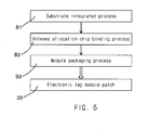
- an electronic tag module patch is formed by a substrate integrated process, an antenna allocation chip bonding process and a module packaging process, wherein in the substrate integrated process a first rigid clip made of an insulating low dielectric coefficient material and provided with a breaking cutline is bonded to a rigid thin-plate substrate made of a low dielectric coefficient material, in the antenna allocation chip bonding process a loop copper foil second antenna or inductance formed by etching and a radio frequency identification chip are attachingly bonded on the first rigid clip, and a plurality of conductive metallic wires made of gold, aluminum and copper are electrically connected between the copper foil second antenna and the radio frequency identification chip on the first rigid clip by wire bonding, and in the module packaging process a second rigid clip which is made of an insulating low dielectric coefficient material and provided with a breaking cutline corresponding to the breaking cutline of the first rigid clip is overlapped on a bottom surface of the first rigid clip so that the copper foil second antenna and the radio frequency identification chip are packaged between the first rigid clip and the second rigid
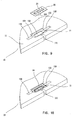
- a mounting surface of the electronic tag module patch is bonded to the resonance chamber of the metallic first antenna and jointed to the metallic ground surface within the concave slot so that the loop copper foil second antenna or inductance is matched to the metallic first antenna at the rectangular recessed portion to generate resonance and induction.
- a colloidal filling glue which is filled in the resonance chamber of the metallic first antenna, the outer slot of the metallic first antenna body and the concave slot attached with the electronic tag module patch by glue dripping or glue filling, is treated by baking and cooling processes in a stove so that the electronic tag module patch is sealed and bound in the metallic first antenna by the cured filling glue and the metallic first antenna is provided with a grinded and embellish glued surface.
- the metallic first antenna treated in the electronic tag sealing process being coated or sprayed on a surface thereof with an anti-interference ceramic paint and treated by baking and cooling processes in the stove so that an anti-interference surface layer is formed on the surface of the metallic first antenna.
- UHF ultra-high-frequency
- Electromagnetic waves radiated from a transmitter can be received by a metallic first antenna.
- the resonance and induction generated by the resonance chamber located in the metallic first antenna and the second antenna of the electronic tag module patch the signal generated can be transmitted to the RFID chip to achieve long-range reading and transmitting effects.
- the breaking cutlines of the first rigid clip located on the second antenna of the electronic tag module patch Due to the breaking cutlines of the first rigid clip located on the second antenna of the electronic tag module patch, the second antenna of the electronic tag module patch is damaged and invalid when the electronic tag module patch glued and sealed in the metallic first antenna is removed by tearing along the breaking cutlines of the first rigid clip, thereby preventing the RFID from being duplicated.
- Another object of the invention is to provide a method for manufacturing a long-range radio frequency identification metallic product, wherein in the metallic first antenna preparation the metallic first antenna is formed by molding the resonance chamber on the metallic first antenna body in the resonance chamber molding manufacturing process, the rectangular recessed portion of the resonance chamber having a width slightly greater than that of the inner slot is downwardly recessed from a plane of the metallic ground surface within the concave slot; in the antenna allocation chip bonding process of the electronic tag module patch preparation the width of the rectangular recessed portion corresponding to the width of the inner slot of the resonance chamber is formed by etching, the rectangular recessed portion has a length is capable of exceeding a rectangular loop copper foil second antenna disposed in the rectangular recessed portion of the resonance chamber, and the loop copper foil second antenna and the radio frequency identification chip are packaged by the bonding of the second rigid clip and the first rigid clip as well as the electronic tag module patch is formed in the module packaging process after the loop copper foil second antenna is electrically connected to the radio frequency identification chip on the first rigid clip; in the electronic tag mounting process the electronic tag module patch
- Still another object of the invention is to provide a method for manufacturing a long-range radio frequency identification metallic product, wherein in the identity surface treatment process the anti-interference surface layer formed on the surface of the metallic first antenna is capable of being printed with characters, numbers or figures thereon, thereby achieving the identifying purpose when performing non-radio identification.
- Yet another object of the invention is to provide a method for manufacturing a long-range radio frequency identification metallic product, wherein in the identity surface treatment process the surface of the metallic first antenna treated in the electronic tag sealing process is capable of being formed with concave or convex characters, numbers or figures by punching and then being coated with the anti-interference ceramic paint or colored, and thus a metallic product such as a plate or vehicle license plate having the electronic tag formed with characters, numbers or figures thereon can be obtained after baking and cooling processes.
- the metallic product structure comprises a metallic first antenna and an electronic tag module patch.
- the metallic first antenna comprises a metallic first antenna body partially or totally made of a metallic plate shape of a metallic product, the metallic first antenna body comprises one sidewall provided with a resonance chamber including a geometry concave slot which is formed on an intersection of two long inner slots and an outer slot and having a height difference with respect to a hole-outer surface and a rectangular recessed portion which is formed on the intersection of the inner slots and the outer slot within the concave slot wherein the two inner slots are parallel to the sidewall of the metallic first antenna body and the outer slot is perpendicular to the sidewall of the metallic first antenna body, an anti-interference ceramic thin film is formed on the surface of the resonance chamber, and an inner surface of the concave slot which is located outside the rectangular recessed portion to be served as a metallic ground surface for the resonance chamber.
- the electronic tag module patch bonded to the metallic ground surface of the resonance chamber of the metallic first antenna and fixedly sealed and bound in the metallic first antenna by a filling glue which is formed in the resonance chamber of the metallic first antenna by glue dripping or glue filling and cured by baking, comprises a thin-plate substrate made of a low dielectric coefficient material, a first rigid clip made of an insulating low dielectric coefficient material and provided with a breaking cutline to be bonded to the thin-plate substrate, a second antenna attachingly bonded on the first rigid clip and served as a rectangular loop copper foil antenna or inductance, a radio frequency identification chip attachingly bonded on the first rigid clip and electrically connected to the second antenna, and a second rigid clip made of an insulating low dielectric coefficient material and provided with a breaking cutline corresponding to the first rigid clip, wherein the second rigid clip is bonded to the first rigid clip so that the second antenna and the radio frequency identification chip are packaged between the first rigid clip and the second rigid clip, and a bottom surface of the second rigid clip is served
- ultra-high-frequency (UHF) RFID skills can be smoothly applied on the various metallic products (e.g., vehicle license plate) without interference.
- Electromagnetic waves radiated from a transmitter can be received by a metallic first antenna.
- the resonance and induction generated by the resonance chamber located in the metallic first antenna and the second antenna of the electronic tag module patch the signal generated can be transmitted to the RFID chip to achieve long-range reading and transmitting effects.
- the breaking cutlines of the first rigid clip located on the second antenna of the electronic tag module patch Due to the breaking cutlines of the first rigid clip located on the second antenna of the electronic tag module patch, the second antenna of the electronic tag module patch is damaged and invalid when the electronic tag module patch glued and sealed in the metallic first antenna is removed by tearing along the breaking cutlines of the first rigid clip, thereby preventing the RFID from being duplicated.
- Yet another object of the invention is to provide a long-range radio frequency identification metallic product structure, wherein the rectangular recessed portion of the resonance chamber of the metallic first antenna having a width slightly greater than that of the inner slot is downwardly recessed from a plane of the metallic ground surface within the concave slot, and the rectangular loop copper foil second antenna of the electronic tag module patch located at the rectangular recessed portion of the resonance chamber of the metallic first antenna has a width corresponding to the width of the inner slot of the resonance chamber and a length capable of exceeding the rectangular recessed portion of the resonance chamber and being averagely extended in the inner slots, so that the loop fold-line second antenna has an ideal field pattern matching with the metallic first antenna on the resonance chamber to generate excellent resonance and induction effects.
- Yet another object of the invention is to provide a long-range radio frequency identification metallic product structure, wherein the electronic tag module patch is fixedly sealed and bound in the metallic first antenna by the cured filling glue, and the metallic first antenna has a grinded and embellish glued surface coated with an anti-interference ceramic paint which is served as an anti-interference surface layer for resisting interference.
- the anti-interference surface layer of the metallic first antenna is printed with characters, numbers or figures thereon, thereby achieving the identifying purpose when performing non-radio identification.
- Yet another object of the invention is to provide a long-range radio frequency identification metallic product structure wherein the electronic tag module patch is fixedly bound in the metallic first antenna, the metallic first antenna has a grinded and embellish glued surface capable of being formed with concave or convex characters, numbers or figures by punching and then being coated with the anti-interference ceramic paint or colored by baking, and thus a metallic product such as a plate or vehicle license plate having the electronic tag formed with characters, numbers or figures thereon can be obtained.
- a method for manufacturing a long-range radio frequency identification (RFID) metallic product at least comprising a metallic first antenna preparation, an electronic tag module patch preparation, an electronic tag mounting process, an electronic tag sealing process, and an identity surface treatment process.
- RFID radio frequency identification
- a metallic first antenna 10 is manufactured by a metallic first antenna body manufacturing process A1, a resonance chamber molding manufacturing process A2 and a resonance chamber surface treating process A3.
- a metallic first antenna body 11 of a predetermined vehicle license plate shape is formed by punching on a metallic plate selected from a metallic product.
- two long inner slots 120 and an outer slot 121 are formed on one sidewall of the metallic first antenna body 11 by punching
- a geometry (rectangular) concave slot 122 is formed on an intersection of the inner slots 120 and the outer slot 121 and having a height difference with respect to a hole-outer surface by punching, forging or machining of computer numerical control (CNC) milling machine
- a rectangular recessed portion 123 molded as a resonance chamber 12 is formed on the intersection of the inner slots 120 and the outer slot 121 within the concave slot 122, wherein an inner surface of the concave slot 122 located outside the rectangular recessed portion 123 is served as a metallic ground surface 124 for the resonance chamber 12.
- an electronic tag module patch 20 is formed by a substrate integrated process B1, an antenna allocation chip bonding process B2 and a module packaging process B3.
- a first rigid clip 22 made of an insulating low dielectric coefficient material and provided with breaking cutlines 220 is bonded to a rigid thin-plate substrate 21 made of a low dielectric coefficient material.
- a loop copper foil second antenna or inductance 23 formed by etching and a radio frequency identification (RFID) chip 24 are attachingly bonded on the first rigid clip 22, and a plurality of conductive metallic wires made of gold, aluminum and copper are electrically connected between the copper foil second antenna 23 and the RFID chip 24 on the first rigid clip 22 by wire bonding.
- RFID radio frequency identification
- a second rigid clip 25 which is made of an insulating low dielectric coefficient material, provided with a breaking cutline and corresponding to the breaking cutline 220 of the first rigid clip 22, is overlapped on a bottom surface of the first rigid clip 22 so that the copper foil second antenna 23 and the RFID chip 24 are packaged between the first rigid clip 22 and the second rigid clip 25.
- a bottom surface of the second rigid clip 25 is served as a mounting surface 250 when the electronic tag module patch 20 and the metallic first antenna 10 are jointed. Note that he thin-plate substrate 21, the first rigid clip 22 and the second rigid clip 25 made by low dielectric coefficient plates can prevent the second antenna 23 from being affected by a large frequency deviation.
- a mounting surface 250 of the electronic tag module patch 20 is bonded to the resonance chamber 12 of the metallic first antenna 10 and jointed to the metallic ground surface 124 within the concave slot 122, so that the loop copper foil second antenna or inductance 23 is matched to the metallic first antenna 10 at the rectangular recessed portion 123 to generate resonance and induction.
- the metallic first antenna 10 treated in the electronic tag sealing process is coated or sprayed on a surface thereof with an anti-interference ceramic paint and treated by baking and cooling processes in the stove, so that an anti-interference surface layer 40 is formed on the surface of the metallic first antenna 10.
- UHF ultra-high-frequency
- the signal generated can be transmitted to the RFID chip 24 so that long-range reading and transmitting effects can be achieved.
- the breaking cutlines 220 of the first rigid clip 22 located on the second antenna 23 of the electronic tag module patch 20 the second antenna 23 of the electronic tag module patch 20 is damaged and invalid when the electronic tag module patch 20 glued and sealed in the metallic first antenna 10 is removed by tearing along the breaking cutlines 220 of the first rigid clip 22, thereby preventing the RFID from being duplicated.
- the metallic first antenna 10 is formed by molding the resonance chamber 12 on the metallic first antenna body 11 in the resonance chamber molding manufacturing process A2, and the rectangular recessed portion 123 of the resonance chamber 12 having a width slightly greater than that of the inner slot 120 is downwardly recessed from a plane of the metallic ground surface 124 within the concave slot 122.
- the width of the rectangular recessed portion 123 corresponding to the width of the inner slot 120 of the resonance chamber 12 is formed by etching, and the rectangular recessed portion 123 has a length capable of exceeding a rectangular loop copper foil second antenna 23 disposed in the rectangular recessed portion 123 of the resonance chamber 12.
- the loop copper foil second antenna 23 is electrically connected to the RFID chip 24 on the first rigid clip 22
- the loop copper foil second antenna 23 and the RFID chip 24 are packaged by the bonding of the second rigid clip 25 and the first rigid clip 22 as well as the electronic tag module patch 20 is formed in the module packaging process.
- the electronic tag module patch 20 is bonded to the metallic ground surface 124 of the concave slot 122 of the resonance chamber 12 of the metallic first antenna 10 in the manner of utilizing the loop copper foil second antenna 23 to be located at the rectangular recessed portion 123 with two ends thereof averagely extended in the inner slots 120, so that the loop fold-line second antenna 23 has an ideal field pattern matching with the metallic first antenna on the resonance chamber 12 to generate excellent resonance and induction effects.
- the second antenna 23 bonded on the first rigid clip 22 is capable of triggering the resonance bandwidth by the loop fold-line thereof.
- the second antenna 23 is a rectangular loop antenna having a length equal to a wavelength.
- radiated field patterns of the whole second antenna 23 are linear polarizations, and the radiation direction is the difference between the radiated field patterns.
- a 90-degree phase difference formed between two orthogonal field patterns is the major condition for forming a circular polarization, and the same amplitude of the electric field and the symmetrical loop antenna structure result in the radiation field with linear polarization.
- Fig. 18 shows a frequency response curve of return loss of the metallic first antenna 10 and the second antenna 23, which is stimulated by HFSS simulation software, wherein the bandwidth is ranged from 820 to 960MHz, and the distribution of the return loss is from -4dB, -9.58dB, -41.48dB, -9.81dB to -4dB.
- Figs. 19 , 20 and 21 show YZ3D, XY3D and XZ3D field pattern diagrams simulated by the simulation software in Fig. 18 .
- a performance testing report of four real samples of electronic tags (vehicle license plates) manufactured by the method in the above-described embodiments is certificated by RFID Solution and Testing Center, Cheng Loong Corp.
- the result of the performance testing report including the standard reading range of 8.85 meters, the reading range of 7.03 meters when the samples are shielded by water, and the reading range approximately ranged from 10.5 to 18.5 meters when the samples are tested in an environment with general space and background, proves that the manufactured RFID metallic products according to the method of the invention surely is characterized with long-range reading effects.
- the manufactured metallic products according to the above-described method of the embodiment can be further treated by following processes.
- the metallic first antenna 10 is formed with an anti-interference surface layer 40 on the surface thereof capable of being printed with characters, numbers or figures (not shown) thereon, thereby achieving the identifying purpose when performing non-radio identification.
- the surface of the metallic first antenna 10 treated in the electronic tag sealing process is capable of being formed with concave or convex characters, numbers or figures (not shown) thereon by punching and then being coated with the anti-interference ceramic paint or colored thereon, and thus a metallic product (e.g., vehicle license plate) having the electronic tag formed with characters, numbers or figures thereon can be obtained after baking and cooling processes.
- a metallic product e.g., vehicle license plate
- the invention provides a long-range radio frequency identification (RFID) metallic product structure.
- the RFID metallic product structure comprises a metallic first antenna 10 and an electronic tag module patch 20.
- the metallic first antenna 10 comprises a metallic first antenna body 11 (e.g., a body of a vehicle license board) partially or totally served by or made of a metallic plate shape of a metallic product, and the metallic first antenna body 11 comprises one sidewall provided with a resonance chamber 12.
- the resonance chamber 12 includes a geometry (rectangular) concave slot 122 which is formed on an intersection of two long inner slots 120 and an outer slot 121 and having a height difference with respect to a hole-outer surface and a rectangular recessed portion 123 which is formed on the intersection of the inner slots 120 and the outer slot 121 within the concave slot 122, wherein the two inner slots 120 are parallel to the sidewall of the metallic first antenna body 11 and the outer slot 121 is perpendicular to the sidewall of the metallic first antenna body 11, an anti-interference ceramic thin film is formed on the surface of the resonance chamber, and an inner surface of the concave slot which is located outside the rectangular recessed portion 123 is served as a metallic ground surface 124 for the resonance chamber 12.
- a geometry (rectangular) concave slot 122 which is formed on an intersection of two long inner slots 120 and an outer slot 121 and having a height difference with respect to a hole-outer surface and a rectangular recessed portion 123 which is formed on the intersection of the inner slots 120
- an electronic tag module patch 20 is bonded to the metallic ground surface 124 of the resonance chamber 12 of the metallic first antenna 10 and fixedly sealed and bound in the metallic first antenna 10 by a filling glue, wherein the filling glue is formed in the resonance chamber 12 of the metallic first antenna 10 by glue dripping or glue filling and cured by baking.
- the electronic tag module patch 20 comprises a thin-plate substrate 21, a first rigid clip 22, a second antenna 23, a radio frequency identification (RFID) chip 24 and a second rigid clip 25.
- the thin-plate substrate 21 is a thin sheet made of a low dielectric coefficient material. As shown in Figs.
- the first rigid clip 22 made of an insulating low dielectric coefficient material and provided with breaking cutlines 220, is bonded to the thin-plate substrate 21.
- the second antenna 23 attachingly bonded on the first rigid clip 22 is served as a rectangular loop copper foil antenna or inductance.
- the RFID chip 24 attachingly bonded on the first rigid clip 22 is electrically connected to the second antenna 23.
- the second rigid clip 25, made of an insulating low dielectric coefficient material and provided with breaking cutline (not shown) corresponding to the first rigid clip 22, is bonded to the first rigid clip 22 so that the second antenna 23 and the RFID chip 24 are packaged between the first rigid clip 22 and the second rigid clip 25.
- a bottom surface of the second rigid clip 25 is served as a mounting surface bonded to the metallic ground surface 124 of the resonance chamber 12 of the metallic first antenna 10.
- the metallic product e.g., vehicle license plates
- UHF ultra-high-frequency
- the signal generated can be transmitted to the RFID chip 24 so that long-range reading and transmitting effects can be achieved.
- the breaking cutlines 220 of the first rigid clip 22 located on the second antenna 23 of the electronic tag module patch 20 the second antenna 23 of the electronic tag module patch 20 is damaged and invalid when the electronic tag module patch 20 glued and sealed in the metallic first antenna 10 is removed by tearing along the breaking cutlines 220 of the first rigid clip 22, thereby preventing the RFID of the metallic product (e.g., vehicle license plates) from being duplicated.
- the rectangular recessed portion 123 of the resonance chamber 12 having a width slightly greater than that of the inner slot 120 is downwardly recessed from a plane of the metallic ground surface 124 within the concave slot 122.
- the rectangular loop copper foil second antenna 23 of the electronic tag module patch 20 is located on the rectangular recessed portion 123 of the resonance chamber 12, the width of the rectangular recessed portion 123 is corresponded to the width of the inner slot 120 of the resonance chamber 12, and the rectangular recessed portion 123 has a length exceeding a rectangular loop copper foil second antenna 23 disposed in the rectangular recessed portion 123 of the resonance chamber 12 and two ends averagely extended in the inner slots 120.
- the loop fold-line second antenna 23 has an ideal field pattern matching with the metallic first antenna on the resonance chamber 12, thereby generating excellent resonance and induction effects.
- the electronic tag module patch 20 is fixedly sealed and bound in the metallic first antenna 10 by the cured filling glue, the metallic first antenna 10 has a grinded and embellish glued surface coated with an anti-interference ceramic paint which is served as an anti-interference surface layer 40 for resisting interference, and the anti-interference surface layer 40 of the metallic first antenna 10 is printed with characters, numbers or figures (not shown) thereon, thereby achieving the identifying purpose when performing non-radio identification.
- the electronic tag module patch 20 is fixedly bound in the metallic first antenna 10, and the metallic first antenna 10 has a grinded and embellish glued surface capable of being formed with concave or convex characters, numbers or figures (not shown) by punching and then being coated with the anti-interference ceramic paint (to form the anti-interference surface layer 40) or colored by baking, and thus a metallic product (e.g., vehicle license plate) having the electronic tag formed with characters, numbers or figures thereon can be obtained after baking and cooling processes.
- a metallic product e.g., vehicle license plate
Landscapes
- Engineering & Computer Science (AREA)
- Computer Hardware Design (AREA)
- Microelectronics & Electronic Packaging (AREA)
- Physics & Mathematics (AREA)
- General Physics & Mathematics (AREA)
- Theoretical Computer Science (AREA)
- Details Of Aerials (AREA)
Description
- The invention relates to a method for manufacturing a long-range radio frequency identification metallic product and a structure thereof, providing long-range reading and transmitting effects and preventing the RFID from being duplicated.
- Radio Frequency Identification (RFID) skills have been widely applied to various fields such as industrial automation, commercial automation, traffic and transportation control management. With the increasing researches related to ultra-high-frequency (UHF) RFID systems, long-range reading and transmitting effect, high efficiency and low cost of RFID skills can be realized. Therefore, with the advantages such as non-contact, low cost, advanced anti-counterfeit and mass-production, the RFID skills has gradually replaced conventional two-dimensional bar code skills in the present markets.
- In general, due to microstrip antennas themselves defectively characterized with narrow band limitation, the majority of microstrip antennas can be limitedly designed as single-frequency and narrow band responses. Taking ultra-high frequency electronic tags, which generally incorporated with printed antennas and mostly being microstrip antennas and printed dipoles, for example, due to signals transmitted from the electronic tags being easily reflected by metallic surfaces to cause signal-receiving abnormalities or even non-motions and signal reading problems, it can be appreciated that the ultra-high frequency electronic tags are actually not suitable for being used in an environment surrounded with metallic objects, such as metallic labels, automobiles, motorcycles, vehicle license plates and electric power facilities. Alternatively, the ultra-high frequency electronic tags, are majorly applied to non-metallic medium surfaces of general merchandise, commodities and books. Basically, the majority of improved electronic tag antennas used for metallic surfaces are based on the conventional electronic tag antennas and skills, such as increasing the size of the electronic tag antenna or increasing the metallic surface distance to reduce the undesired effects to the electronic tag antenna caused by the metallic reflective surfaces, or adopting the standardized slotting method to combine with the electronic tags. In the method of increasing the size of the electronic tag antenna or increasing the metallic surface distance to reduce the undesired effects to the electronic tag antenna caused by the metallic reflective surfaces, the height or distance between the electronic tag and the metallic surface shall be kept over than 2.5 mm. In this way, the reading distance of the electronic tag can be increased, but the total cost of the electronic tag is increased and the bandwidth of the antenna is reduced, and also the undesired effects to the electronic tag antenna caused by the metallic reflective surfaces still cannot be eliminated. In view of this, the conventional electronic tag antennas are almost applied for the places with non-metallic surfaces. For example, Electronic Toll Collection (ETC) in Taiwan and the designs of general identification tags. On the other hand, in the combination technique of the standardized slotting method and the electronic tags, the reliability and smoothness of the product are relatively unstable and uncontrollable, and particularly the joint points between the chip and the metallic contacts of the metallic antenna are separated from each other due to the property of thermal expansion and cold shrinkage and long-term operation. In this design, impedance matching shall be performed between each of the metallic antennas and the chip, or the frequency bias or field pattern variations are possibly occurred. In general, joint points between the chip and the metallic contacts of the metallic antenna are treated by conductive glue adhering, copper pouring, copper electroplating and vacuum copper sputtering, etc. Taking the conductive glue for example, the lift span of the conductive glue in the room temperature is about two to five years. If the conductive glue is hardened or oxidized, a certain resistance is formed in the bonding layer disposed between the hardened conductive materials and the neighboring materials in the conductive glue, and the resistance of the accumulated conductive materials in the conductive glue results in the rising of the VF value and a bulky change of the frequency bias and field pattern variation. Thus, it is difficult to control the credibility of the conductive glue with respect to lift span and temperature. The problems caused by the copper pouring method are slightly similar to that of the conductive glue adhering method. In the copper electroplating method, due to the different expansion coefficients of aluminum material and the copper material, the chip and the metallic antenna are possibly separated from each other caused by the peeling of the electroplated copper layer. In the vacuum copper sputtering method, the vacuum copper sputtering method has a stability superior to the copper electroplating method, but the operation cost is extremely high when dealing with the large-sized product with a small sputtering area. Besides, when the electronic tag is combined to the antenna by the standardized slotting method, it is usually that the connection of the electronic tag and the antenna cannot be prevented from crashing, scratching, moistening and stealing.
- Ceramic dielectric microstrip antenna is applicable to metallic surfaces, capable of providing high dielectric constant to obtain a minimized antenna size and utilizing the metallic surface as an extended reflective surface to stabilize the performance and to increase directivity, but not suitable for being the economic electronic tag due to its high manufacturing cost. Alternatively, an artificial magnetic conductor (AMC) structure, characterized with high impedance to generate a magnetic-flow direction between the AMC structure and the economic electronic tag identical to that between the metallic surface and the AMC structure, can be laminated between an antenna radiation surface and the metallic surface to increase the reading range and gains of the economic electronic tag, but the AMC skills are still in experimental stage due to its difficulty and high cost.
- To prevent the signals of ultra-high-frequency (UHF) RFID from being spoilt by interference from the metallic surface or parts, the invention provides a metallic plate of a metallic product to be a metallic first antenna body and constitutes a first antenna by forming a resonance chamber on the metallic first antenna body. In an electronic tag module preparation, a small-sized microstrip loop metallic second antenna provided with breaking cutlines is bonded to and sealed in the metallic first antenna so that the second antenna is matching with the metallic first antenna on the resonance chamber. With an anti-interference treatment on the surface of the metallic first antenna, an ultra-high-frequency (UHF) RFID disposed in a radio frequency identification (RFID) metallic product is capable of being normally operated without interference from the metallic surface and providing excellent converted field patterns, effectively attaining a ten-meter long-range reading and transmitting effects. Further, due to the design of the breaking cutlines on the second antenna of the electronic tag module patch, the second antenna of the electronic tag module patch is damaged and invalid when the electronic tag module patch is removed by tearing along the breaking cutlines, thereby preventing the RFID from being removed and duplicated.
- An object of the invention is to provide a method for manufacturing a long-range radio frequency identification metallic product. The method of the invention at least comprises a metallic first antenna preparation, an electronic tag module patch preparation, an electronic tag mounting process, an electronic tag sealing process and an identity surface treatment process. In the metallic first antenna preparation a metallic first antenna is manufactured by a metallic first antenna body manufacturing process, a resonance chamber molding manufacturing process and a resonance chamber surface treating process. In the metallic first antenna body manufacturing process a metallic first antenna body of a predetermined shape is formed by punching on a metallic plate selected from a metallic product. In the resonance chamber molding manufacturing process two long inner slots and an outer slot are formed on one sidewall of the metallic first antenna body by punching, a geometry concave slot is formed on an intersection of the inner slots and the outer slot and having a height difference with respect to a hole-outer surface by punching or forging or machining of computer numerical control milling machine, and a rectangular recessed portion molded as a resonance chamber is formed on the intersection of the inner slots and the outer slot within the concave slot, wherein an inner surface of the concave slot located outside the rectangular recessed portion is served as a metallic ground surface for the resonance chamber. In the resonance chamber surface treating process a surface of the resonance chamber surface is treated by a ceramic processing so that an anti-interference ceramic thin film is formed on the surface of the resonance chamber. In the electronic tag module patch preparation an electronic tag module patch is formed by a substrate integrated process, an antenna allocation chip bonding process and a module packaging process, wherein in the substrate integrated process a first rigid clip made of an insulating low dielectric coefficient material and provided with a breaking cutline is bonded to a rigid thin-plate substrate made of a low dielectric coefficient material, in the antenna allocation chip bonding process a loop copper foil second antenna or inductance formed by etching and a radio frequency identification chip are attachingly bonded on the first rigid clip, and a plurality of conductive metallic wires made of gold, aluminum and copper are electrically connected between the copper foil second antenna and the radio frequency identification chip on the first rigid clip by wire bonding, and in the module packaging process a second rigid clip which is made of an insulating low dielectric coefficient material and provided with a breaking cutline corresponding to the breaking cutline of the first rigid clip is overlapped on a bottom surface of the first rigid clip so that the copper foil second antenna and the radio frequency identification chip are packaged between the first rigid clip and the second rigid clip, and a bottom surface of the second rigid clip is served as a mounting surface when the electronic tag module patch and the metallic first antenna are jointed. In the electronic tag mounting process a mounting surface of the electronic tag module patch is bonded to the resonance chamber of the metallic first antenna and jointed to the metallic ground surface within the concave slot so that the loop copper foil second antenna or inductance is matched to the metallic first antenna at the rectangular recessed portion to generate resonance and induction. In the electronic tag sealing process a colloidal filling glue, which is filled in the resonance chamber of the metallic first antenna, the outer slot of the metallic first antenna body and the concave slot attached with the electronic tag module patch by glue dripping or glue filling, is treated by baking and cooling processes in a stove so that the electronic tag module patch is sealed and bound in the metallic first antenna by the cured filling glue and the metallic first antenna is provided with a grinded and embellish glued surface. In the identity surface treatment process the metallic first antenna treated in the electronic tag sealing process being coated or sprayed on a surface thereof with an anti-interference ceramic paint and treated by baking and cooling processes in the stove so that an anti-interference surface layer is formed on the surface of the metallic first antenna. With the fulfillment of the above-described manufacturing processes, ultra-high-frequency (UHF) RFID skills can be smoothly applied on the various metallic products (e.g., vehicle license plate) without interference. Electromagnetic waves radiated from a transmitter can be received by a metallic first antenna. With the resonance and induction generated by the resonance chamber located in the metallic first antenna and the second antenna of the electronic tag module patch, the signal generated can be transmitted to the RFID chip to achieve long-range reading and transmitting effects. Due to the breaking cutlines of the first rigid clip located on the second antenna of the electronic tag module patch, the second antenna of the electronic tag module patch is damaged and invalid when the electronic tag module patch glued and sealed in the metallic first antenna is removed by tearing along the breaking cutlines of the first rigid clip, thereby preventing the RFID from being duplicated.
- Another object of the invention is to provide a method for manufacturing a long-range radio frequency identification metallic product, wherein in the metallic first antenna preparation the metallic first antenna is formed by molding the resonance chamber on the metallic first antenna body in the resonance chamber molding manufacturing process, the rectangular recessed portion of the resonance chamber having a width slightly greater than that of the inner slot is downwardly recessed from a plane of the metallic ground surface within the concave slot; in the antenna allocation chip bonding process of the electronic tag module patch preparation the width of the rectangular recessed portion corresponding to the width of the inner slot of the resonance chamber is formed by etching, the rectangular recessed portion has a length is capable of exceeding a rectangular loop copper foil second antenna disposed in the rectangular recessed portion of the resonance chamber, and the loop copper foil second antenna and the radio frequency identification chip are packaged by the bonding of the second rigid clip and the first rigid clip as well as the electronic tag module patch is formed in the module packaging process after the loop copper foil second antenna is electrically connected to the radio frequency identification chip on the first rigid clip; in the electronic tag mounting process the electronic tag module patch is bonded to the metallic ground surface of the concave slot of the resonance chamber of the metallic first antenna in the manner of utilizing the loop copper foil second antenna to be located at the rectangular recessed portion with two ends thereof averagely extended in the inner slots so that the loop fold-line second antenna has an ideal field pattern matching with the metallic first antenna on the resonance chamber, thereby generating excellent resonance and induction effects.
- Still another object of the invention is to provide a method for manufacturing a long-range radio frequency identification metallic product, wherein in the identity surface treatment process the anti-interference surface layer formed on the surface of the metallic first antenna is capable of being printed with characters, numbers or figures thereon, thereby achieving the identifying purpose when performing non-radio identification.
- Yet another object of the invention is to provide a method for manufacturing a long-range radio frequency identification metallic product, wherein in the identity surface treatment process the surface of the metallic first antenna treated in the electronic tag sealing process is capable of being formed with concave or convex characters, numbers or figures by punching and then being coated with the anti-interference ceramic paint or colored, and thus a metallic product such as a plate or vehicle license plate having the electronic tag formed with characters, numbers or figures thereon can be obtained after baking and cooling processes.
- Yet another object of the invention is to provide a long-range radio frequency identification metallic product structure. The metallic product structure comprises a metallic first antenna and an electronic tag module patch. The metallic first antenna comprises a metallic first antenna body partially or totally made of a metallic plate shape of a metallic product, the metallic first antenna body comprises one sidewall provided with a resonance chamber including a geometry concave slot which is formed on an intersection of two long inner slots and an outer slot and having a height difference with respect to a hole-outer surface and a rectangular recessed portion which is formed on the intersection of the inner slots and the outer slot within the concave slot wherein the two inner slots are parallel to the sidewall of the metallic first antenna body and the outer slot is perpendicular to the sidewall of the metallic first antenna body, an anti-interference ceramic thin film is formed on the surface of the resonance chamber, and an inner surface of the concave slot which is located outside the rectangular recessed portion to be served as a metallic ground surface for the resonance chamber. The electronic tag module patch, bonded to the metallic ground surface of the resonance chamber of the metallic first antenna and fixedly sealed and bound in the metallic first antenna by a filling glue which is formed in the resonance chamber of the metallic first antenna by glue dripping or glue filling and cured by baking, comprises a thin-plate substrate made of a low dielectric coefficient material, a first rigid clip made of an insulating low dielectric coefficient material and provided with a breaking cutline to be bonded to the thin-plate substrate, a second antenna attachingly bonded on the first rigid clip and served as a rectangular loop copper foil antenna or inductance, a radio frequency identification chip attachingly bonded on the first rigid clip and electrically connected to the second antenna, and a second rigid clip made of an insulating low dielectric coefficient material and provided with a breaking cutline corresponding to the first rigid clip, wherein the second rigid clip is bonded to the first rigid clip so that the second antenna and the radio frequency identification chip are packaged between the first rigid clip and the second rigid clip, and a bottom surface of the second rigid clip is served as a mounting surface bonded to the metallic ground surface of the resonance chamber of the metallic first antenna. With the metallic product manufactured by the above-described structure, ultra-high-frequency (UHF) RFID skills can be smoothly applied on the various metallic products (e.g., vehicle license plate) without interference. Electromagnetic waves radiated from a transmitter can be received by a metallic first antenna. With the resonance and induction generated by the resonance chamber located in the metallic first antenna and the second antenna of the electronic tag module patch, the signal generated can be transmitted to the RFID chip to achieve long-range reading and transmitting effects. Due to the breaking cutlines of the first rigid clip located on the second antenna of the electronic tag module patch, the second antenna of the electronic tag module patch is damaged and invalid when the electronic tag module patch glued and sealed in the metallic first antenna is removed by tearing along the breaking cutlines of the first rigid clip, thereby preventing the RFID from being duplicated.
- Yet another object of the invention is to provide a long-range radio frequency identification metallic product structure, wherein the rectangular recessed portion of the resonance chamber of the metallic first antenna having a width slightly greater than that of the inner slot is downwardly recessed from a plane of the metallic ground surface within the concave slot, and the rectangular loop copper foil second antenna of the electronic tag module patch located at the rectangular recessed portion of the resonance chamber of the metallic first antenna has a width corresponding to the width of the inner slot of the resonance chamber and a length capable of exceeding the rectangular recessed portion of the resonance chamber and being averagely extended in the inner slots, so that the loop fold-line second antenna has an ideal field pattern matching with the metallic first antenna on the resonance chamber to generate excellent resonance and induction effects.
- Yet another object of the invention is to provide a long-range radio frequency identification metallic product structure, wherein the electronic tag module patch is fixedly sealed and bound in the metallic first antenna by the cured filling glue, and the metallic first antenna has a grinded and embellish glued surface coated with an anti-interference ceramic paint which is served as an anti-interference surface layer for resisting interference. The anti-interference surface layer of the metallic first antenna is printed with characters, numbers or figures thereon, thereby achieving the identifying purpose when performing non-radio identification.
- Yet another object of the invention is to provide a long-range radio frequency identification metallic product structure wherein the electronic tag module patch is fixedly bound in the metallic first antenna, the metallic first antenna has a grinded and embellish glued surface capable of being formed with concave or convex characters, numbers or figures by punching and then being coated with the anti-interference ceramic paint or colored by baking, and thus a metallic product such as a plate or vehicle license plate having the electronic tag formed with characters, numbers or figures thereon can be obtained.
- The above and other objects, features and advantages of the invention will become apparent from the following detailed description taken with the accompanying drawings.
-
-
Fig. 1 is a schematic view showing the process of the invention; -
Fig. 2 is a schematic view showing the preparation flowchart of a metallic first antenna of the invention; -
Fig. 3 is a perspective schematic view showing the structure of a metallic first antenna of the invention; -
Fig. 4 is a perspective schematic view showing the structure of a resonance chamber of a metallic first antenna of the invention; -
Fig. 5 is a schematic view showing the preparation flowchart of an electronic tag module patch of the invention; -
Fig. 6 is an exploded schematic view showing the package structure of an electronic tag module patch of the invention; -
Fig. 7 is a schematic view showing the structure of a first rigid clip of an electronic tag module patch of the invention; -
Fig. 8 is a schematic view showing the status of an electronic tag module patch of the invention, wherein a first rigid clip is attachingly bonded with an antenna and a chip; -
Fig. 9 is a perspective schematic view showing the bonding relationship of an electronic tag module patch and a resonance chamber of the invention; -
Fig. 10 is a schematic view showing the status of an electronic tag module patch bonded to a resonance chamber of the invention; -
Fig. 11 is a schematic view showing the sectional structure of a packaged, attached electronic tag module patch of the invention; -
Fig. 12 shows a pattern embodiment of a completed metallic product of the invention; -
Fig. 13 is a schematic view showing the sectional structure of an electronic tag module patch sealed in a metallic first antenna and operation relationship of the invention; -
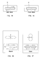
Fig. 14 is a schematic view showing a rectangular loop of a second antenna of the invention when a signal source is in an odd mode; -
Fig. 15 is a schematic view showing a rectangular loop of a second antenna of the invention when a signal source is in an even mode; -
Fig. 16 is a schematic view showing an radiated field patterns of the whole second antenna of the invention when a signal source is in an odd mode; -
Fig. 17 is a schematic view showing a radiated field pattern of the whole second antenna of the invention when a signal source is in an even mode; -
Fig. 18 is a frequency response curve of the return loss of a metallic first antenna and a second antenna of the invention, which is stimulated by HFSS simulation software; -
Fig. 19 is a YZ3D field pattern diagram simulated by the simulation software inFig. 18 ; -
Fig. 20 is a XY3D field pattern diagram simulated by the simulation software inFig. 18 ; and -
Fig. 21 is a XZ3D field pattern diagram simulated by the simulation software inFig. 18 . - Referring to
Fig. 1 , a method for manufacturing a long-range radio frequency identification (RFID) metallic product, at least comprising a metallic first antenna preparation, an electronic tag module patch preparation, an electronic tag mounting process, an electronic tag sealing process, and an identity surface treatment process. - Referring to
Fig. 2 , in the metallic first antenna preparation, a metallicfirst antenna 10 is manufactured by a metallic first antenna body manufacturing process A1, a resonance chamber molding manufacturing process A2 and a resonance chamber surface treating process A3. - Referring to
Fig. 3 , in the metallic first antenna body manufacturing process, a metallicfirst antenna body 11 of a predetermined vehicle license plate shape is formed by punching on a metallic plate selected from a metallic product. - Referring to
Fig. 4 in conjunction withFigs. 2 ,3 , in the resonance chamber molding manufacturing process A2, two longinner slots 120 and anouter slot 121 are formed on one sidewall of the metallicfirst antenna body 11 by punching, a geometry (rectangular)concave slot 122 is formed on an intersection of theinner slots 120 and theouter slot 121 and having a height difference with respect to a hole-outer surface by punching, forging or machining of computer numerical control (CNC) milling machine, and a rectangular recessedportion 123 molded as aresonance chamber 12 is formed on the intersection of theinner slots 120 and theouter slot 121 within theconcave slot 122, wherein an inner surface of theconcave slot 122 located outside the rectangular recessedportion 123 is served as ametallic ground surface 124 for theresonance chamber 12. In the resonance chamber surface treating process A3, a surface of theresonance chamber surface 12 is treated by a ceramic processing so that an anti-interference ceramic thin film is formed on the surface of theresonance chamber 12. As shown inFigs. 1 and5 , in the electronic tag module patch preparation, an electronictag module patch 20 is formed by a substrate integrated process B1, an antenna allocation chip bonding process B2 and a module packaging process B3. - Referring to
Figs. 5 ,6 and 7 , in the substrate integrated process B1, a firstrigid clip 22 made of an insulating low dielectric coefficient material and provided with breakingcutlines 220 is bonded to a rigid thin-plate substrate 21 made of a low dielectric coefficient material. As shown inFigs. 5 ,6 and 8 , in the antenna allocation chip bonding process B2, a loop copper foil second antenna orinductance 23 formed by etching and a radio frequency identification (RFID)chip 24 are attachingly bonded on the firstrigid clip 22, and a plurality of conductive metallic wires made of gold, aluminum and copper are electrically connected between the copper foilsecond antenna 23 and theRFID chip 24 on the firstrigid clip 22 by wire bonding. - As shown in
Figs. 5 ,6 and 7 , in the module packaging process B3, a secondrigid clip 25, which is made of an insulating low dielectric coefficient material, provided with a breaking cutline and corresponding to thebreaking cutline 220 of the firstrigid clip 22, is overlapped on a bottom surface of the firstrigid clip 22 so that the copper foilsecond antenna 23 and theRFID chip 24 are packaged between the firstrigid clip 22 and the secondrigid clip 25. - As shown in
Figs. 6 and9 , in the electronic tag mounting process, a bottom surface of the secondrigid clip 25 is served as a mountingsurface 250 when the electronictag module patch 20 and the metallicfirst antenna 10 are jointed. Note that he thin-plate substrate 21, the firstrigid clip 22 and the secondrigid clip 25 made by low dielectric coefficient plates can prevent thesecond antenna 23 from being affected by a large frequency deviation. - As shown in
Figs. 1 and9 , in the electronic tag mounting process, a mountingsurface 250 of the electronictag module patch 20 is bonded to theresonance chamber 12 of the metallicfirst antenna 10 and jointed to themetallic ground surface 124 within theconcave slot 122, so that the loop copper foil second antenna orinductance 23 is matched to the metallicfirst antenna 10 at the rectangular recessedportion 123 to generate resonance and induction. - As shown in
Figs. 1 ,10 and11 , in the electronic tag sealing process, acolloidal filling glue 30, which is filled in theresonance chamber 12 of the metallicfirst antenna 10, theouter slot 121 of the metallicfirst antenna body 11, and theconcave slot 122 attached with the electronictag module patch 20 by glue dripping or glue filling, is treated by baking and cooling processes in a stove, so that the electronictag module patch 20 is sealed and bound in the metallicfirst antenna 10 by the cured filling glue, and the metallicfirst antenna 10 is provided with a grinded and embellish glued surface. - As shown in
Figs. 1 ,11 and 12 , in the identity surface treatment process, the metallicfirst antenna 10 treated in the electronic tag sealing process is coated or sprayed on a surface thereof with an anti-interference ceramic paint and treated by baking and cooling processes in the stove, so that ananti-interference surface layer 40 is formed on the surface of the metallicfirst antenna 10. According to the above-described manufacturing processes, ultra-high-frequency (UHF) RFID skills can be smoothly applied on the various metallic products (e.g., vehicle license plates) without interference, and therefore the electromagnetic waves radiated from a transmitter can be received by the metallic first antenna 10 (e.g., metallic vehicle license plates). - As shown in
Fig. 13 , with the resonance and induction generated by theresonance chamber 12 located in the metallicfirst antenna 10 and thesecond antenna 23 of the electronictag module patch 20, the signal generated can be transmitted to theRFID chip 24 so that long-range reading and transmitting effects can be achieved. Further, due to the breakingcutlines 220 of the firstrigid clip 22 located on thesecond antenna 23 of the electronictag module patch 20, thesecond antenna 23 of the electronictag module patch 20 is damaged and invalid when the electronictag module patch 20 glued and sealed in the metallicfirst antenna 10 is removed by tearing along the breakingcutlines 220 of the firstrigid clip 22, thereby preventing the RFID from being duplicated. - According to the above-described method in the embodiment and as shown in
Figs. 1, 2 ,3 and 4 , in the metallic first antenna preparation, the metallicfirst antenna 10 is formed by molding theresonance chamber 12 on the metallicfirst antenna body 11 in the resonance chamber molding manufacturing process A2, and the rectangular recessedportion 123 of theresonance chamber 12 having a width slightly greater than that of theinner slot 120 is downwardly recessed from a plane of themetallic ground surface 124 within theconcave slot 122. - As shown in
Figs. 1 ,5 ,6 and13 , in the antenna allocation chip bonding process 132 of the electronic tag module patch preparation, the width of the rectangular recessedportion 123 corresponding to the width of theinner slot 120 of theresonance chamber 12 is formed by etching, and the rectangular recessedportion 123 has a length capable of exceeding a rectangular loop copper foilsecond antenna 23 disposed in the rectangular recessedportion 123 of theresonance chamber 12. - As shown in
Fig. 8 , after the loop copper foilsecond antenna 23 is electrically connected to theRFID chip 24 on the firstrigid clip 22, the loop copper foilsecond antenna 23 and theRFID chip 24 are packaged by the bonding of the secondrigid clip 25 and the firstrigid clip 22 as well as the electronictag module patch 20 is formed in the module packaging process. - As shown in
Figs. 1 ,9 ,10 and13 , in the electronic tag mounting process, the electronictag module patch 20 is bonded to themetallic ground surface 124 of theconcave slot 122 of theresonance chamber 12 of the metallicfirst antenna 10 in the manner of utilizing the loop copper foilsecond antenna 23 to be located at the rectangular recessedportion 123 with two ends thereof averagely extended in theinner slots 120, so that the loop fold-linesecond antenna 23 has an ideal field pattern matching with the metallic first antenna on theresonance chamber 12 to generate excellent resonance and induction effects. - According to the method in the embodiment, the
second antenna 23 bonded on the firstrigid clip 22 is capable of triggering the resonance bandwidth by the loop fold-line thereof. InFigs. 14 and 15 , thesecond antenna 23 is a rectangular loop antenna having a length equal to a wavelength. As shown inFigs. 16 and 17 , when a signal source is in an even or odd mode, radiated field patterns of the wholesecond antenna 23 are linear polarizations, and the radiation direction is the difference between the radiated field patterns. A 90-degree phase difference formed between two orthogonal field patterns is the major condition for forming a circular polarization, and the same amplitude of the electric field and the symmetrical loop antenna structure result in the radiation field with linear polarization. -
Fig. 18 shows a frequency response curve of return loss of the metallicfirst antenna 10 and thesecond antenna 23, which is stimulated by HFSS simulation software, wherein the bandwidth is ranged from 820 to 960MHz, and the distribution of the return loss is from -4dB, -9.58dB, -41.48dB, -9.81dB to -4dB. -
Figs. 19 ,20 and21 show YZ3D, XY3D and XZ3D field pattern diagrams simulated by the simulation software inFig. 18 . - A performance testing report of four real samples of electronic tags (vehicle license plates) manufactured by the method in the above-described embodiments is certificated by RFID Solution and Testing Center, Cheng Loong Corp. The result of the performance testing report, including the standard reading range of 8.85 meters, the reading range of 7.03 meters when the samples are shielded by water, and the reading range approximately ranged from 10.5 to 18.5 meters when the samples are tested in an environment with general space and background, proves that the manufactured RFID metallic products according to the method of the invention surely is characterized with long-range reading effects.
- Additionally, for increasing appearance effects or purposes, the manufactured metallic products according to the above-described method of the embodiment can be further treated by following processes. As shown in
Figs. 1 and12 , in the identity surface treatment process, the metallicfirst antenna 10 is formed with ananti-interference surface layer 40 on the surface thereof capable of being printed with characters, numbers or figures (not shown) thereon, thereby achieving the identifying purpose when performing non-radio identification. Further, the surface of the metallicfirst antenna 10 treated in the electronic tag sealing process is capable of being formed with concave or convex characters, numbers or figures (not shown) thereon by punching and then being coated with the anti-interference ceramic paint or colored thereon, and thus a metallic product (e.g., vehicle license plate) having the electronic tag formed with characters, numbers or figures thereon can be obtained after baking and cooling processes. - Further, according to the above-described method of the embodiment, the invention provides a long-range radio frequency identification (RFID) metallic product structure. As shown in
Figs. 3, 4 and9 , the RFID metallic product structure comprises a metallicfirst antenna 10 and an electronictag module patch 20. The metallicfirst antenna 10 comprises a metallic first antenna body 11 (e.g., a body of a vehicle license board) partially or totally served by or made of a metallic plate shape of a metallic product, and the metallicfirst antenna body 11 comprises one sidewall provided with aresonance chamber 12. In the metallicfirst antenna body 11, theresonance chamber 12 includes a geometry (rectangular)concave slot 122 which is formed on an intersection of two longinner slots 120 and anouter slot 121 and having a height difference with respect to a hole-outer surface and a rectangular recessedportion 123 which is formed on the intersection of theinner slots 120 and theouter slot 121 within theconcave slot 122, wherein the twoinner slots 120 are parallel to the sidewall of the metallicfirst antenna body 11 and theouter slot 121 is perpendicular to the sidewall of the metallicfirst antenna body 11, an anti-interference ceramic thin film is formed on the surface of the resonance chamber, and an inner surface of the concave slot which is located outside the rectangular recessedportion 123 is served as ametallic ground surface 124 for theresonance chamber 12. - As shown in
Figs. 9, 10 and11 , an electronictag module patch 20 is bonded to themetallic ground surface 124 of theresonance chamber 12 of the metallicfirst antenna 10 and fixedly sealed and bound in the metallicfirst antenna 10 by a filling glue, wherein the filling glue is formed in theresonance chamber 12 of the metallicfirst antenna 10 by glue dripping or glue filling and cured by baking. As shown inFig. 6 , the electronictag module patch 20 comprises a thin-plate substrate 21, a firstrigid clip 22, asecond antenna 23, a radio frequency identification (RFID)chip 24 and a secondrigid clip 25. As shown inFigs. 6 and 7 , the thin-plate substrate 21 is a thin sheet made of a low dielectric coefficient material. As shown inFigs. 6 and 8 , the firstrigid clip 22, made of an insulating low dielectric coefficient material and provided with breakingcutlines 220, is bonded to the thin-plate substrate 21. Thesecond antenna 23 attachingly bonded on the firstrigid clip 22 is served as a rectangular loop copper foil antenna or inductance. TheRFID chip 24 attachingly bonded on the firstrigid clip 22 is electrically connected to thesecond antenna 23. The secondrigid clip 25, made of an insulating low dielectric coefficient material and provided with breaking cutline (not shown) corresponding to the firstrigid clip 22, is bonded to the firstrigid clip 22 so that thesecond antenna 23 and theRFID chip 24 are packaged between the firstrigid clip 22 and the secondrigid clip 25. - Referring to
Fig. 9 again, a bottom surface of the secondrigid clip 25 is served as a mounting surface bonded to themetallic ground surface 124 of theresonance chamber 12 of the metallicfirst antenna 10. As shown inFig. 12 , by providing the metallic product (e.g., vehicle license plates) formed by the above-described structure, ultra-high-frequency (UHF) RFID skills can be smoothly applied on the various metallic products (e.g., vehicle license plates) without interference. As shown inFig. 11 and 13 , with the electromagnetic waves radiated from a transmitter to be received by the metallicfirst antenna 10 and with the resonance and induction generated by theresonance chamber 12 located in the metallicfirst antenna 10 and thesecond antenna 23 of the electronictag module patch 20, the signal generated can be transmitted to theRFID chip 24 so that long-range reading and transmitting effects can be achieved. Further, due to the breakingcutlines 220 of the firstrigid clip 22 located on thesecond antenna 23 of the electronictag module patch 20, thesecond antenna 23 of the electronictag module patch 20 is damaged and invalid when the electronictag module patch 20 glued and sealed in the metallicfirst antenna 10 is removed by tearing along the breakingcutlines 220 of the firstrigid clip 22, thereby preventing the RFID of the metallic product (e.g., vehicle license plates) from being duplicated. - According to the above-described embodiment and as shown in
Figs. 3 and 4 , in the metallicfirst antenna 10, the rectangular recessedportion 123 of theresonance chamber 12 having a width slightly greater than that of theinner slot 120 is downwardly recessed from a plane of themetallic ground surface 124 within theconcave slot 122. As shown inFig. 13 , the rectangular loop copper foilsecond antenna 23 of the electronictag module patch 20 is located on the rectangular recessedportion 123 of theresonance chamber 12, the width of the rectangular recessedportion 123 is corresponded to the width of theinner slot 120 of theresonance chamber 12, and the rectangular recessedportion 123 has a length exceeding a rectangular loop copper foilsecond antenna 23 disposed in the rectangular recessedportion 123 of theresonance chamber 12 and two ends averagely extended in theinner slots 120. The loop fold-linesecond antenna 23 has an ideal field pattern matching with the metallic first antenna on theresonance chamber 12, thereby generating excellent resonance and induction effects. - According to the above-described embodiment and as shown in
Figs. 11 and 12 , the electronictag module patch 20 is fixedly sealed and bound in the metallicfirst antenna 10 by the cured filling glue, the metallicfirst antenna 10 has a grinded and embellish glued surface coated with an anti-interference ceramic paint which is served as ananti-interference surface layer 40 for resisting interference, and theanti-interference surface layer 40 of the metallicfirst antenna 10 is printed with characters, numbers or figures (not shown) thereon, thereby achieving the identifying purpose when performing non-radio identification. - According to the above-described embodiment and as shown in
Figs. 11 and 12 , the electronictag module patch 20 is fixedly bound in the metallicfirst antenna 10, and the metallicfirst antenna 10 has a grinded and embellish glued surface capable of being formed with concave or convex characters, numbers or figures (not shown) by punching and then being coated with the anti-interference ceramic paint (to form the anti-interference surface layer 40) or colored by baking, and thus a metallic product (e.g., vehicle license plate) having the electronic tag formed with characters, numbers or figures thereon can be obtained after baking and cooling processes. - While the invention has been described in terms of preferred embodiments, those skilled in the art will recognize that the invention can be practiced with modifications within the scope of the appended claims.
Claims (9)
- A method for manufacturing a long-range radio frequency identification metallic product, comprising the steps of:a metallic first antenna preparation, an electronic tag module patch preparation, an electronic tag mounting process, an electronic tag sealing process and an identity surface treatment process;in the metallic first antenna preparation a metallic first antenna being manufactured by a metallic first antenna body manufacturing process, a resonance chamber molding manufacturing process and a resonance chamber surface treating process;in the metallic first antenna body manufacturing process a metallic first antenna body of a predetermined shape being formed by punching on a metallic plate selected from a metallic product;in the resonance chamber molding manufacturing process two long inner slots and an outer slot being formed on one sidewall of the metallic first antenna body by punching, a geometry concave slot being formed on an intersection of the inner slots and the outer slot and having a height difference with respect to a hole-outer surface by punching or forging or machining of computer numerical control milling machine, and a rectangular recessed portion molded as a resonance chamber being formed on the intersection of the inner slots and the outer slot within the concave slot, wherein an inner surface of the concave slot located outside the rectangular recessed portion is served as a metallic ground surface for the resonance chamber;in the resonance chamber surface treating process a surface of the resonance chamber surface being treated by a ceramic processing so that an anti-interference ceramic thin film is formed on the surface of the resonance chamber;in the electronic tag module patch preparation an electronic tag module patch being formed by a substrate integrated process, an antenna allocation chip bonding process and a module packaging process, wherein in the substrate integrated process a first rigid clip made of an insulating low dielectric coefficient material and provided with a breaking cutline is bonded to a rigid thin-plate substrate made of a low dielectric coefficient material, in the antenna allocation chip bonding process a loop copper foil second antenna or inductance formed by etching and a radio frequency identification chip are attachingly bonded on the first rigid clip, and a plurality of conductive metallic wires made of gold, aluminum and copper are electrically connected between the copper foil second antenna and the radio frequency identification chip on the first rigid clip by wire bonding, and in the module packaging process a second rigid clip which is made of an insulating low dielectric coefficient material and provided with a breaking cutline corresponding to the breaking cutline of the first rigid clip is overlapped on a bottom surface of the first rigid clip so that the copper foil second antenna and the radio frequency identification chip are packaged between the first rigid clip and the second rigid clip, and a bottom surface of the second rigid clip is served as a mounting surface when the electronic tag module patch and the metallic first antenna are jointed;in the electronic tag mounting process a mounting surface of the electronic tag module patch being bonded to the resonance chamber of the metallic first antenna and jointed to the metallic ground surface within the concave slot so that the loop copper foil second antenna or inductance is matched to the metallic first antenna at the rectangular recessed portion to generate resonance and induction;in the electronic tag sealing process a colloidal filling glue, which is filled in the resonance chamber of the metallic first antenna, the outer slot of the metallic first antenna body and the concave slot attached with the electronic tag module patch by glue dripping or glue filling, is treated by baking and cooling processes in a stove so that the electronic tag module patch is sealed and bound in the metallic first antenna by the cured filling glue and the metallic first antenna is provided with a grinded and embellish glued surface; andin the identity surface treatment process the metallic first antenna treated in the electronic tag sealing process being coated or sprayed on a surface thereof with an anti-interference ceramic paint and treated by baking and cooling processes in the stove so that an anti-interference surface layer is formed on the surface of the metallic first antenna.
- The method for manufacturing a long-range radio frequency identification metallic product as claimed in claim 1, wherein
in the metallic first antenna preparation the metallic first antenna is formed by molding the resonance chamber on the metallic first antenna body in the resonance chamber molding manufacturing process, the rectangular recessed portion of the resonance chamber having a width slightly greater than that of the inner slot is downwardly recessed from a plane of the metallic ground surface within the concave slot;
in the antenna allocation chip bonding process of the electronic tag module patch preparation the width of the rectangular recessed portion corresponding to the width of the inner slot of the resonance chamber is formed by etching, the rectangular recessed portion has a length is capable of exceeding a rectangular loop copper foil second antenna disposed in the rectangular recessed portion of the resonance chamber, and the loop copper foil second antenna and the radio frequency identification chip are packaged by the bonding of the second rigid clip and the first rigid clip as well as the electronic tag module patch is formed in the module packaging process after the loop copper foil second antenna is electrically connected to the radio frequency identification chip on the first rigid clip; and
in the electronic tag mounting process the electronic tag module patch is bonded to the metallic ground surface of the concave slot of the resonance chamber of the metallic first antenna in the manner of utilizing the loop copper foil second antenna to be located at the rectangular recessed portion with two ends thereof averagely extended in the inner slots so that the loop fold-line second antenna has an ideal field pattern matching with the metallic first antenna on the resonance chamber. - The method for manufacturing a long-range radio frequency identification metallic product as claimed in claim 1, wherein in the identity surface treatment process the anti-interference surface layer formed on the surface of the metallic first antenna is capable of being printed with characters, numbers or figures thereon.
- The method for manufacturing a long-range radio frequency identification metallic product as claimed in claim 1, wherein in the identity surface treatment process the surface of the metallic first antenna treated in the electronic tag sealing process is capable of being formed with concave or convex characters, numbers or figures by punching and then being coated with the anti-interference ceramic paint or colored.
- A long-range radio frequency identification metallic product structure, comprising:a metallic first antenna (10), comprising a metallic first antenna body (11) partially or totally made of a metallic plate shape of a metallic product, the metallic first antenna body (11) comprising one sidewall provided with a resonance chamber (12) including a geometry concave slot (122) which is formed on an intersection of two long inner slots (120) and an outer slot (121) and having a height difference with respect to a hole-outer surface and a rectangular recessed portion (123) which is formed on the intersection of the inner slots (120) and the outer slot (121) within the concave slot wherein the two inner slots (120) are parallel to the sidewall of the metallic first antenna body (11) and the outer slot (121) is perpendicular to the sidewall of the metallic first antenna body (11), an anti-interference ceramic thin film being formed on the surface of the resonance chamber (12), and an inner surface of the concave slot (122) which is located outside the rectangular recessed portion (123) to be served as a metallic ground surface (124) for the resonance chamber (12); andan electronic tag module patch (20) bonded to the metallic ground surface of the resonance chamber (12) of the metallic first antenna (10) and fixedly sealed and bound in the metallic first antenna (10) by a filling glue which is formed in the resonance chamber (12) of the metallic first antenna (10) by glue dripping or glue filling and cured by baking, comprising a thin-plate substrate (21) made of a low dielectric coefficient material, a first rigid clip (22) made of an insulating low dielectric coefficient material and provided with a breaking cutline (220) to be bonded to the thin-plate substrate (21), a second antenna (23) attachingly bonded on the first rigid clip (22) and served as a rectangular loop copper foil antenna (23) or inductance, a radio frequency identification chip (24) attachingly bonded on the first rigid clip (22) and electrically connected to the second antenna (23), and a second rigid clip (25) made of an insulating low dielectric coefficient material and provided with a breaking cutline corresponding to the first rigid clip (22), wherein the second rigid clip (25) is bonded to the first rigid clip (22) so that the second antenna (23) and the radio frequency identification chip (24) are packaged between the first rigid clip (22) and the second rigid clip (25), and a bottom surface of the second rigid clip (25) is served as a mounting surface (250) bonded to the metallic ground surface (124) of the resonance chamber (12) of the metallic first antenna (10).
- The long-range radio frequency identification metallic product structure as claimed in claim 5, wherein the rectangular recessed portion (123) of the resonance chamber (12) of the metallic first antenna (10) having a width slightly greater than that of the inner slot (120) is downwardly recessed from a plane of the metallic ground surface (124) within the concave slot (122), and the rectangular loop copper foil second antenna (23) of the electronic tag module patch (20) located at the rectangular recessed portion (123) of the resonance chamber (12) of the metallic first antenna (10) has a width corresponding to the width of the inner slot (120) of the resonance chamber (12) and a length capable of exceeding the rectangular recessed portion (123) of the resonance chamber (12) and being averagely extended in the inner slots (120).
- The long-range radio frequency identification metallic product structure as claimed in claim 5, wherein the electronic tag module patch (20) is fixedly sealed and bound in the metallic first antenna (10) by the cured filling glue, and the metallic first antenna (10) has a grinded and embellish glued surface coated with an anti-interference ceramic paint which is served as an anti-interference surface layer for resisting interference.
- The long-range radio frequency identification metallic product structure as claimed in claim 7, wherein the anti-interference surface layer of the metallic first antenna (10) is printed with characters, numbers or figures thereon.
- The long-range radio frequency identification metallic product structure as claimed in claim 5, wherein the electronic tag module patch (20) is fixedly bound in the metallic first antenna (10), and the metallic first antenna (10) has a grinded and embellish glued surface capable of being formed with concave or convex characters, numbers or figures by punching and then being coated with the anti-interference ceramic paint or colored by baking.
Priority Applications (1)
| Application Number | Priority Date | Filing Date | Title |
|---|---|---|---|
| EP20120173184 EP2677475B1 (en) | 2012-06-22 | 2012-06-22 | Method for manufacturing long-range radio frequency identification metallic product and structure thereof |
Applications Claiming Priority (1)
| Application Number | Priority Date | Filing Date | Title |
|---|---|---|---|
| EP20120173184 EP2677475B1 (en) | 2012-06-22 | 2012-06-22 | Method for manufacturing long-range radio frequency identification metallic product and structure thereof |
Publications (2)
| Publication Number | Publication Date |
|---|---|
| EP2677475A1 EP2677475A1 (en) | 2013-12-25 |
| EP2677475B1 true EP2677475B1 (en) | 2014-11-19 |
Family
ID=46578833
Family Applications (1)
| Application Number | Title | Priority Date | Filing Date |
|---|---|---|---|
| EP20120173184 Active EP2677475B1 (en) | 2012-06-22 | 2012-06-22 | Method for manufacturing long-range radio frequency identification metallic product and structure thereof |
Country Status (1)
| Country | Link |
|---|---|
| EP (1) | EP2677475B1 (en) |
Families Citing this family (4)
| Publication number | Priority date | Publication date | Assignee | Title |
|---|---|---|---|---|
| CN105470645A (en) * | 2016-02-06 | 2016-04-06 | 蚌埠日月仪器研究所有限公司 | Antenna sealing structure of data collecting device |
| CN106156834A (en) * | 2016-06-27 | 2016-11-23 | 浙江立芯信息科技股份有限公司 | A kind of Anti-scrape label |
| TWI624995B (en) * | 2016-09-09 | 2018-05-21 | Read Tag Tech Corp | Long-range radio frequency anti-metal identification tag |
| TWI646468B (en) * | 2017-05-01 | 2019-01-01 | 永豐泰科技企業有限公司 | Vehicle listing wireless electronic identifier |
Family Cites Families (4)
| Publication number | Priority date | Publication date | Assignee | Title |
|---|---|---|---|---|
| DE102006028827A1 (en) * | 2006-06-21 | 2008-01-10 | Dynamic Systems Gmbh | Transponder with electronic memory chip and magnetic loop antenna |
| NL1032542C2 (en) * | 2006-09-20 | 2008-03-21 | Knieriem B V J | Vehicle identification. |
| DE202008001549U1 (en) * | 2008-02-04 | 2008-05-29 | Harting Ag | RFID transponder |
| JP5018918B2 (en) * | 2010-03-17 | 2012-09-05 | パナソニック株式会社 | ANTENNA DEVICE AND PORTABLE TERMINAL DEVICE USING THE SAME |
-
2012
- 2012-06-22 EP EP20120173184 patent/EP2677475B1/en active Active
Also Published As
| Publication number | Publication date |
|---|---|
| EP2677475A1 (en) | 2013-12-25 |
Similar Documents
| Publication | Publication Date | Title |
|---|---|---|
| US8381998B1 (en) | Method for manufacturing long-range radio frequency identification product and structure thereof | |
| US10312570B2 (en) | Long-distance radio frequency anti-metal identification tag | |
| CA2621574C (en) | Rfid transponder | |
| JP4173904B2 (en) | SECURITY TAG HAVING 3D ANTENNA AREA COMPOSED OF FLAT Pedestal, AND MANUFACTURING METHOD | |
| CN102542326B (en) | Manufacturing method and structure of long-distance radio frequency identification metal product | |
| US20130043316A1 (en) | Miniaturized Radio-Frequency Identification Tag and Microstrip Patch Antenna Thereof | |
| AU782197B2 (en) | Electronic label | |
| EP2283539B1 (en) | Rfid tag | |
| JP2010074809A (en) | Antenna structure for rfid transponder | |
| TW200816057A (en) | RFID tag and manufacturing method thereof | |
| KR20070098420A (en) | Rfid tag and manufacturing method thereof | |
| EP2677475B1 (en) | Method for manufacturing long-range radio frequency identification metallic product and structure thereof | |
| CN110768002B (en) | Anti-metal radio frequency identification tag antenna | |
| WO2006078147A1 (en) | Thin rfid tag for radio frequency identification | |
| US7764240B2 (en) | Antenna configuration for RFID tags | |
| TW201322541A (en) | Manufacturing method and structure of long-range RF wireless identification metal products | |
| TW201820208A (en) | Miniaturized anti-metal electronic tag with long read distance for achieving the effect of resisting metal interference and providing long read distance, with a convenient usage condition that is simple and miniaturized without occupying much space | |
| CN202548885U (en) | Long-distance radio frequency identification metal product structure | |
| Karuppuswami et al. | A 3D printed UHF passive RFID tag for plastic components | |
| JP5061712B2 (en) | Non-contact IC tag manufacturing method | |
| JP2005078114A (en) | Non-contact type data carrier | |
| JP7176313B2 (en) | RF tag label | |
| JP2020046838A (en) | RF tag label | |
| JP2020046834A (en) | RF tag label | |
| CN219591642U (en) | Integrated antenna |
Legal Events
| Date | Code | Title | Description |
|---|---|---|---|
| PUAI | Public reference made under article 153(3) epc to a published international application that has entered the european phase |
Free format text: ORIGINAL CODE: 0009012 |
|
| AK | Designated contracting states |
Kind code of ref document: A1 Designated state(s): AL AT BE BG CH CY CZ DE DK EE ES FI FR GB GR HR HU IE IS IT LI LT LU LV MC MK MT NL NO PL PT RO RS SE SI SK SM TR |
|
| AX | Request for extension of the european patent |
Extension state: BA ME |
|
| 17P | Request for examination filed |
Effective date: 20140331 |
|
| RBV | Designated contracting states (corrected) |
Designated state(s): AL AT BE BG CH CY CZ DE DK EE ES FI FR GB GR HR HU IE IS IT LI LT LU LV MC MK MT NL NO PL PT RO RS SE SI SK SM TR |
|
| RIC1 | Information provided on ipc code assigned before grant |
Ipc: H01Q 1/22 20060101ALI20140429BHEP Ipc: H01Q 7/00 20060101ALI20140429BHEP Ipc: H01Q 13/10 20060101ALI20140429BHEP Ipc: G06K 19/077 20060101AFI20140429BHEP |
|
| GRAP | Despatch of communication of intention to grant a patent |
Free format text: ORIGINAL CODE: EPIDOSNIGR1 |
|
| INTG | Intention to grant announced |
Effective date: 20140606 |
|
| GRAS | Grant fee paid |
Free format text: ORIGINAL CODE: EPIDOSNIGR3 |
|
| GRAA | (expected) grant |
Free format text: ORIGINAL CODE: 0009210 |
|
| AK | Designated contracting states |
Kind code of ref document: B1 Designated state(s): AL AT BE BG CH CY CZ DE DK EE ES FI FR GB GR HR HU IE IS IT LI LT LU LV MC MK MT NL NO PL PT RO RS SE SI SK SM TR |
|
| REG | Reference to a national code |
Ref country code: GB Ref legal event code: FG4D |
|
| REG | Reference to a national code |
Ref country code: CH Ref legal event code: EP |
|
| REG | Reference to a national code |
Ref country code: AT Ref legal event code: REF Ref document number: 697398 Country of ref document: AT Kind code of ref document: T Effective date: 20141215 |
|
| REG | Reference to a national code |
Ref country code: IE Ref legal event code: FG4D |
|
| REG | Reference to a national code |
Ref country code: DE Ref legal event code: R096 Ref document number: 602012003841 Country of ref document: DE Effective date: 20141224 |
|
| REG | Reference to a national code |
Ref country code: NL Ref legal event code: VDEP Effective date: 20141119 |
|
| REG | Reference to a national code |
Ref country code: AT Ref legal event code: MK05 Ref document number: 697398 Country of ref document: AT Kind code of ref document: T Effective date: 20141119 |
|
| REG | Reference to a national code |
Ref country code: LT Ref legal event code: MG4D |
|
| PG25 | Lapsed in a contracting state [announced via postgrant information from national office to epo] |
Ref country code: NL Free format text: LAPSE BECAUSE OF FAILURE TO SUBMIT A TRANSLATION OF THE DESCRIPTION OR TO PAY THE FEE WITHIN THE PRESCRIBED TIME-LIMIT Effective date: 20141119 Ref country code: NO Free format text: LAPSE BECAUSE OF FAILURE TO SUBMIT A TRANSLATION OF THE DESCRIPTION OR TO PAY THE FEE WITHIN THE PRESCRIBED TIME-LIMIT Effective date: 20150219 Ref country code: PT Free format text: LAPSE BECAUSE OF FAILURE TO SUBMIT A TRANSLATION OF THE DESCRIPTION OR TO PAY THE FEE WITHIN THE PRESCRIBED TIME-LIMIT Effective date: 20150319 Ref country code: ES Free format text: LAPSE BECAUSE OF FAILURE TO SUBMIT A TRANSLATION OF THE DESCRIPTION OR TO PAY THE FEE WITHIN THE PRESCRIBED TIME-LIMIT Effective date: 20141119 Ref country code: LT Free format text: LAPSE BECAUSE OF FAILURE TO SUBMIT A TRANSLATION OF THE DESCRIPTION OR TO PAY THE FEE WITHIN THE PRESCRIBED TIME-LIMIT Effective date: 20141119 Ref country code: IS Free format text: LAPSE BECAUSE OF FAILURE TO SUBMIT A TRANSLATION OF THE DESCRIPTION OR TO PAY THE FEE WITHIN THE PRESCRIBED TIME-LIMIT Effective date: 20150319 Ref country code: FI Free format text: LAPSE BECAUSE OF FAILURE TO SUBMIT A TRANSLATION OF THE DESCRIPTION OR TO PAY THE FEE WITHIN THE PRESCRIBED TIME-LIMIT Effective date: 20141119 |
|
| PG25 | Lapsed in a contracting state [announced via postgrant information from national office to epo] |
Ref country code: HR Free format text: LAPSE BECAUSE OF FAILURE TO SUBMIT A TRANSLATION OF THE DESCRIPTION OR TO PAY THE FEE WITHIN THE PRESCRIBED TIME-LIMIT Effective date: 20141119 Ref country code: SE Free format text: LAPSE BECAUSE OF FAILURE TO SUBMIT A TRANSLATION OF THE DESCRIPTION OR TO PAY THE FEE WITHIN THE PRESCRIBED TIME-LIMIT Effective date: 20141119 Ref country code: GR Free format text: LAPSE BECAUSE OF FAILURE TO SUBMIT A TRANSLATION OF THE DESCRIPTION OR TO PAY THE FEE WITHIN THE PRESCRIBED TIME-LIMIT Effective date: 20150220 Ref country code: CY Free format text: LAPSE BECAUSE OF FAILURE TO SUBMIT A TRANSLATION OF THE DESCRIPTION OR TO PAY THE FEE WITHIN THE PRESCRIBED TIME-LIMIT Effective date: 20141119 Ref country code: PL Free format text: LAPSE BECAUSE OF FAILURE TO SUBMIT A TRANSLATION OF THE DESCRIPTION OR TO PAY THE FEE WITHIN THE PRESCRIBED TIME-LIMIT Effective date: 20141119 Ref country code: AT Free format text: LAPSE BECAUSE OF FAILURE TO SUBMIT A TRANSLATION OF THE DESCRIPTION OR TO PAY THE FEE WITHIN THE PRESCRIBED TIME-LIMIT Effective date: 20141119 Ref country code: LV Free format text: LAPSE BECAUSE OF FAILURE TO SUBMIT A TRANSLATION OF THE DESCRIPTION OR TO PAY THE FEE WITHIN THE PRESCRIBED TIME-LIMIT Effective date: 20141119 Ref country code: RS Free format text: LAPSE BECAUSE OF FAILURE TO SUBMIT A TRANSLATION OF THE DESCRIPTION OR TO PAY THE FEE WITHIN THE PRESCRIBED TIME-LIMIT Effective date: 20141119 |
|
| PG25 | Lapsed in a contracting state [announced via postgrant information from national office to epo] |
Ref country code: CZ Free format text: LAPSE BECAUSE OF FAILURE TO SUBMIT A TRANSLATION OF THE DESCRIPTION OR TO PAY THE FEE WITHIN THE PRESCRIBED TIME-LIMIT Effective date: 20141119 Ref country code: SK Free format text: LAPSE BECAUSE OF FAILURE TO SUBMIT A TRANSLATION OF THE DESCRIPTION OR TO PAY THE FEE WITHIN THE PRESCRIBED TIME-LIMIT Effective date: 20141119 Ref country code: EE Free format text: LAPSE BECAUSE OF FAILURE TO SUBMIT A TRANSLATION OF THE DESCRIPTION OR TO PAY THE FEE WITHIN THE PRESCRIBED TIME-LIMIT Effective date: 20141119 Ref country code: RO Free format text: LAPSE BECAUSE OF FAILURE TO SUBMIT A TRANSLATION OF THE DESCRIPTION OR TO PAY THE FEE WITHIN THE PRESCRIBED TIME-LIMIT Effective date: 20141119 Ref country code: DK Free format text: LAPSE BECAUSE OF FAILURE TO SUBMIT A TRANSLATION OF THE DESCRIPTION OR TO PAY THE FEE WITHIN THE PRESCRIBED TIME-LIMIT Effective date: 20141119 |
|
| REG | Reference to a national code |
Ref country code: DE Ref legal event code: R097 Ref document number: 602012003841 Country of ref document: DE |
|
| PLBE | No opposition filed within time limit |
Free format text: ORIGINAL CODE: 0009261 |
|
| STAA | Information on the status of an ep patent application or granted ep patent |
Free format text: STATUS: NO OPPOSITION FILED WITHIN TIME LIMIT |
|
| 26N | No opposition filed |
Effective date: 20150820 |
|
| PG25 | Lapsed in a contracting state [announced via postgrant information from national office to epo] |
Ref country code: IT Free format text: LAPSE BECAUSE OF FAILURE TO SUBMIT A TRANSLATION OF THE DESCRIPTION OR TO PAY THE FEE WITHIN THE PRESCRIBED TIME-LIMIT Effective date: 20141119 |
|
| PG25 | Lapsed in a contracting state [announced via postgrant information from national office to epo] |
Ref country code: MC Free format text: LAPSE BECAUSE OF FAILURE TO SUBMIT A TRANSLATION OF THE DESCRIPTION OR TO PAY THE FEE WITHIN THE PRESCRIBED TIME-LIMIT Effective date: 20141119 |
|
| REG | Reference to a national code |
Ref country code: CH Ref legal event code: PL |
|
| PG25 | Lapsed in a contracting state [announced via postgrant information from national office to epo] |
Ref country code: SI Free format text: LAPSE BECAUSE OF FAILURE TO SUBMIT A TRANSLATION OF THE DESCRIPTION OR TO PAY THE FEE WITHIN THE PRESCRIBED TIME-LIMIT Effective date: 20141119 Ref country code: LU Free format text: LAPSE BECAUSE OF FAILURE TO SUBMIT A TRANSLATION OF THE DESCRIPTION OR TO PAY THE FEE WITHIN THE PRESCRIBED TIME-LIMIT Effective date: 20150622 |
|
| REG | Reference to a national code |
Ref country code: IE Ref legal event code: MM4A |
|
| PG25 | Lapsed in a contracting state [announced via postgrant information from national office to epo] |
Ref country code: CH Free format text: LAPSE BECAUSE OF NON-PAYMENT OF DUE FEES Effective date: 20150630 Ref country code: IE Free format text: LAPSE BECAUSE OF NON-PAYMENT OF DUE FEES Effective date: 20150622 Ref country code: LI Free format text: LAPSE BECAUSE OF NON-PAYMENT OF DUE FEES Effective date: 20150630 |
|
| REG | Reference to a national code |
Ref country code: FR Ref legal event code: PLFP Year of fee payment: 5 |
|
| PG25 | Lapsed in a contracting state [announced via postgrant information from national office to epo] |
Ref country code: MT Free format text: LAPSE BECAUSE OF FAILURE TO SUBMIT A TRANSLATION OF THE DESCRIPTION OR TO PAY THE FEE WITHIN THE PRESCRIBED TIME-LIMIT Effective date: 20141119 |
|
| PG25 | Lapsed in a contracting state [announced via postgrant information from national office to epo] |
Ref country code: BG Free format text: LAPSE BECAUSE OF FAILURE TO SUBMIT A TRANSLATION OF THE DESCRIPTION OR TO PAY THE FEE WITHIN THE PRESCRIBED TIME-LIMIT Effective date: 20141119 Ref country code: SM Free format text: LAPSE BECAUSE OF FAILURE TO SUBMIT A TRANSLATION OF THE DESCRIPTION OR TO PAY THE FEE WITHIN THE PRESCRIBED TIME-LIMIT Effective date: 20141119 Ref country code: HU Free format text: LAPSE BECAUSE OF FAILURE TO SUBMIT A TRANSLATION OF THE DESCRIPTION OR TO PAY THE FEE WITHIN THE PRESCRIBED TIME-LIMIT; INVALID AB INITIO Effective date: 20120622 |
|
| PG25 | Lapsed in a contracting state [announced via postgrant information from national office to epo] |
Ref country code: TR Free format text: LAPSE BECAUSE OF FAILURE TO SUBMIT A TRANSLATION OF THE DESCRIPTION OR TO PAY THE FEE WITHIN THE PRESCRIBED TIME-LIMIT Effective date: 20141119 |
|
| PG25 | Lapsed in a contracting state [announced via postgrant information from national office to epo] |
Ref country code: BE Free format text: LAPSE BECAUSE OF FAILURE TO SUBMIT A TRANSLATION OF THE DESCRIPTION OR TO PAY THE FEE WITHIN THE PRESCRIBED TIME-LIMIT Effective date: 20141119 |
|
| REG | Reference to a national code |
Ref country code: FR Ref legal event code: PLFP Year of fee payment: 6 |
|
| REG | Reference to a national code |
Ref country code: DE Ref legal event code: R082 Ref document number: 602012003841 Country of ref document: DE Representative=s name: VIERING, JENTSCHURA & PARTNER MBB PATENT- UND , DE Ref country code: DE Ref legal event code: R081 Ref document number: 602012003841 Country of ref document: DE Owner name: RFID INTEGRATED MARKETING CO., LTD., TW Free format text: FORMER OWNER: JOIN YIUH INDUSTRY CO., LTD., TAICHUNG CITY, TW |
|
| REG | Reference to a national code |
Ref country code: GB Ref legal event code: 732E Free format text: REGISTERED BETWEEN 20180301 AND 20180307 |
|
| REG | Reference to a national code |
Ref country code: FR Ref legal event code: PLFP Year of fee payment: 7 |
|
| PG25 | Lapsed in a contracting state [announced via postgrant information from national office to epo] |
Ref country code: MK Free format text: LAPSE BECAUSE OF FAILURE TO SUBMIT A TRANSLATION OF THE DESCRIPTION OR TO PAY THE FEE WITHIN THE PRESCRIBED TIME-LIMIT Effective date: 20141119 |
|
| REG | Reference to a national code |
Ref country code: FR Ref legal event code: TP Owner name: RFID INTEGRATED MARKETING CO, LTD., TW Effective date: 20180724 |
|
| PG25 | Lapsed in a contracting state [announced via postgrant information from national office to epo] |
Ref country code: AL Free format text: LAPSE BECAUSE OF FAILURE TO SUBMIT A TRANSLATION OF THE DESCRIPTION OR TO PAY THE FEE WITHIN THE PRESCRIBED TIME-LIMIT Effective date: 20141119 |
|
| PGFP | Annual fee paid to national office [announced via postgrant information from national office to epo] |
Ref country code: GB Payment date: 20240530 Year of fee payment: 13 |
|
| PGFP | Annual fee paid to national office [announced via postgrant information from national office to epo] |
Ref country code: DE Payment date: 20240613 Year of fee payment: 13 |
|
| PGFP | Annual fee paid to national office [announced via postgrant information from national office to epo] |
Ref country code: FR Payment date: 20240607 Year of fee payment: 13 |