EP2677351A1 - Method of manufacturing a diffraction grating - Google Patents
Method of manufacturing a diffraction grating Download PDFInfo
- Publication number
- EP2677351A1 EP2677351A1 EP13172844.6A EP13172844A EP2677351A1 EP 2677351 A1 EP2677351 A1 EP 2677351A1 EP 13172844 A EP13172844 A EP 13172844A EP 2677351 A1 EP2677351 A1 EP 2677351A1
- Authority
- EP
- European Patent Office
- Prior art keywords
- grating
- plane
- diffraction grating
- crystalline material
- blazed
- Prior art date
- Legal status (The legal status is an assumption and is not a legal conclusion. Google has not performed a legal analysis and makes no representation as to the accuracy of the status listed.)
- Granted
Links
Images



Classifications
-
- G—PHYSICS
- G02—OPTICS
- G02B—OPTICAL ELEMENTS, SYSTEMS OR APPARATUS
- G02B5/00—Optical elements other than lenses
- G02B5/18—Diffraction gratings
- G02B5/1847—Manufacturing methods
- G02B5/1852—Manufacturing methods using mechanical means, e.g. ruling with diamond tool, moulding
-
- G—PHYSICS
- G02—OPTICS
- G02B—OPTICAL ELEMENTS, SYSTEMS OR APPARATUS
- G02B5/00—Optical elements other than lenses
- G02B5/18—Diffraction gratings
Definitions
- the present invention relates to a method of manufacturing a diffraction grating.
- a diffraction grating may be used, for example, in an optical apparatus such as a spectroscope.
- a phase diffraction grating is a diffraction grating made so that a phase difference is given to incident light in one cycle of grating by making the shape of a grating groove into a blazed shape, a sinusoidal shape, or a rectangular wave shape so that a diffraction light intensity property can be selected according to its use.
- a blazed diffraction grating is a phase diffraction grating having a grating groove with a triangular cross-section, and is manufactured by sequentially forming a ruling, with a grating groove of a predetermined cross-sectional shape, by a cutting process using a grind stone or a shaving process using a diamond cutting tool.
- a blazed diffraction grating made of a crystalline material is a diffraction grating designed to use high-order diffraction light.
- the machining in which the grating groove is formed is performed in a ductile mode.
- a critical cutting thickness determines a boundary between the ductile mode and a brittle mode. It is known that the critical cutting thickness depends on a relation between a crystal orientation of a slip surface and a worked surface, a relation between a crystal axis and a cutting direction, and a relation between the crystal axis and a cutting force direction (which depends on a tool rake angle and the cutting direction) in a crystal.
- the grating groove is formed by using a groove processing surface (a surface on which the grating groove is to be formed) as a (111) plane, using a cutting direction as a (111) plane in a crystalline material made of Si or Ge, and using a single crystal diamond cutting tool in an ultra-precision cutting process.
- a groove processing surface a surface on which the grating groove is to be formed
- a cutting direction as a (111) plane in a crystalline material made of Si or Ge
- the blazed diffraction grating is influenced by at least one of the long side and the short side that constitute the grating groove when the blazed diffraction grating is used as a transmission type or an immersion type (backside reflection type).
- the surface roughness (profile irregularity) of the short side is important in the case of a reflection diffraction grating.
- the crystalline materials made of gallium phosphide (GaP) or gallium arsenide (GaAs) are used as optical materials, but the machining in which the grating groove of a blazed diffraction grating is formed from these crystalline materials has not been proposed.
- a blazed diffraction grating as set out in accompanying claim 10.
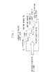
- Fig. 1 is a schematic cross-sectional view illustrating a blazed diffraction grating according to an embodiment of the present invention.
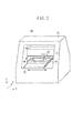
- Fig. 2 is a schematic perspective view illustrating a processing machine according to the embodiment of the present invention.
- Fig. 3 is a schematic cross-sectional view illustrating a method of manufacturing the blazed diffraction grating illustrated in Fig. 1 .
- Fig. 4 is a flowchart illustrating the method of manufacturing the blazed diffraction grating illustrated in Fig. 1 .
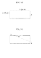
- Figs. 5A, 5B , 5C, and 5D are cross-sectional views of a workpiece in respective steps in Fig. 4 .
- Fig. 1 is a schematic cross-sectional view illustrating a blazed diffraction grating (sometimes called an Echelle diffraction grating) 10 that diffracts incident light.
- the blazed diffraction grating is a diffraction grating in which a grating groove has a saw tooth shape (blazed shape), and has a high diffraction efficiency for a specific order and wavelength.
- the blazed diffraction grating of the present embodiment is an immersion diffraction grating (transmission type, backside reflection diffraction grating) as illustrated in Fig. 1 .
- the blazed diffraction grating 10 may also be configured as a reflection diffraction grating that reflects the light on its front surface.
- Each grating of the blazed diffraction grating 10 has an asymmetric triangular shape composed of a short side 11 and a long side 12 in a cross-section including a blazed direction BD and a grating normal GN perpendicular thereto.
- the short side 11 and the long side 12 each also extend in a direction perpendicular to the plane of the page in Fig. 1 .
- the apex angle 13 is approximately equal to an opening angle ⁇ 1 of a tip portion of a cutting tool described below.
- a surface 16 having the short side 11 works as a blazed plane that receives the most incident light
- a surface 15 having the long side 12 works a counter plane adj acent to the blazed plane among the surfaces that constitute each grating.
- the surface 15 may work as the blazed plane and the surface 16 may work as the counter plane in some cases.
- the present invention is also applicable to the case where each grating does not have the triangular shape in the cross-section including the blazed direction BD and the grating normal perpendicular thereto.
- the blazed diffraction grating 10 is often used in a configuration so that the incident light direction L of the light faces the short side in order to resolve the incident light frequently as possible, and the diffraction efficiency depends on the surface accuracy (profile irregularity) of the short side 11. Thus, it is required to process the surface 16 including the short side 11 with high precision.
- Fig. 2 is a schematic perspective view of a processing machine 20 of the present embodiment, and X, Y and Z are set for three axis directions that are orthogonal to one another.
- the processing machine 20 is a manufacture apparatus that manufactures the blazed diffraction grating 10 by forming a plurality of grating grooves 17 on the workpiece W made of a GaP crystalline material or a GaAs crystalline material.
- the GaP crystalline material transmits the light from visible light of 0.5 to 16 ⁇ m to far-infrared light.
- the GaAs crystalline material transmits the light of 1 to 18 ⁇ m and infrared light. Thus, they are suitable as an optical element for the infrared light.
- GaP and GaAs are compounds of Ga in a group 13 with P and As, respectively, in a group 15 in the periodic table of the elements, and have the same crystal structure referred to as Zincblende (B3).
- Zincblende (B3) Zincblende
- both materials can be used for the present embodiment.
- the crystal orientations are not completely uniform, and thus it is difficult to stably obtain a processing property depending on a crystal axis. Thus, it is difficult to obtain a good optical surface from the polycrystalline material. Therefore, it is more desirable to use single crystal crystalline material of GaP or GaAs.
- the processing machine 20 is an ultraprecision cutting processing machine that can perform numerical control (NC) of cutting to a typical accuracy of several tens of nanometers(nm).
- the processing machine 20 forms the grating groove 17 by using a diamond cutting tool 22 that has a sharp tip and produces a processing transcription property with high accuracy as a tool in a shaper (plane shaving) system in which the surface is cut by moving a cutting blade.
- the workpiece is mounted on an XY stage composed of an X stage 25 movable in an X direction and a Y stage 26 movable in a Y direction in a highly rigid housing 21, which is resistant to external vibration.
- the diamond cutting tool 22 is mounted on a Z stage movable in a Z direction. In the present embodiment, the diamond cutting tool is not rotated, but a processing machine in which the diamond cutting tool is rotated could also be used.
- Fig. 3 is a schematic cross-sectional view of the processing machine 20, the workpiece W, and the diamond cutting tool 22.
- a cutting tool feeding plain surface represented by M is parallel to a brazed direction, which is parallel to a cutting tool feeding direction where the diamond cutting tool 22 is moved relative to the workpiece W.
- the diamond cutting tool has at least two edge cutting blades 23 and 24, which transfer a polygonal groove cross-sectional shape that works as the grating groove 17.
- An angle ⁇ 1 made by tips of the edge cutting blades 23 and 24 is approximately equal to an opening angle ⁇ of the grating groove 17, and is 90° in the present embodiment.
- a tip portion of the edge cutting blades 23 and 24 is scarcely rounded and a ridgeline accuracy of the edge is very high in the tip portion.
- a wall accuracy of the grating groove in the blazed diffraction grating 10 can be made highly precise.
- the diamond cutting tool 22 is slid down on a side of the workpiece so that a cutting depth in the Z direction at a position where the diamond cutting tool 22 is located opposite the workpiece W is, for example, 0.2 ⁇ m, and the XY stage is moved in the X or Y direction in a linear or curved manner.
- a cutting rate is obtained by relative movement of the diamond cutting tool 22 and the workpiece W, and the workpiece W is cut and processed with the edge cutting blades 23 and 24.
- a movement target may be a side of the cutting tool or a side of the workpiece in the machining.
- the cutting depth required in the Z direction is divided and a step of forming a divided cutting depth may be repeated multiple times.
- oil mist is sprayed from a backside of a cutting tool rake face to flush cutting chips from the rake face while processing heat is removed.
- FIG. 4 is a flowchart illustrating the method of manufacturing (machining) the diffraction grating using the processing machine 20.
- Figs. 5A, 5B , 5C, and 5D are schematic cross-sectional views of the workpiece W in respective steps in Fig. 4 .
- a workpiece (work) W made of a crystalline material of GaP or GaAs having an appropriate shape such as a cylindrical shape, a cubic shape or a rectangular shape is obtained as illustrated in Fig. 5A .
- the workpiece W having a cubic shape can be obtained by utilizing a crystal growing apparatus.
- the workpiece W having a rectangular shape in which both an upper surface (upper side end face) and a left side end face are crystal orientation (110) planes is obtained.
- step S120 the workpiece W obtained in step S110 is cut as illustrated by a dot line D in Fig. 5B .
- a slope angle of this dot line D against the upper surface is 20° as an example.
- a cutting processing machine used in step S120 is not the processing machine 20, and a processing machine with lower accuracy is used.
- step S130 the cut surface C of the workpiece W in step S120 is ground using a grinding apparatus P as illustrated in Fig. 5C .
- the workpiece W may be placed in the grinding apparatus using a jig 30 to be used in step S140.
- step S140 the ground workpiece W is placed on the aforementioned XY stage in the processing machine 20 through the jig 30 as illustrated in Fig. 5D .
- the jig 30 has the slope angle of 20°, and thus the machined surface becomes parallel to the surface of the Y stage 26.
- the workpiece W is placed on the jig 30 with a slant to be mounted in the processing machine 20 so that the workpiece has the slope angle of 20 degrees against the cutting tool feeding plain surface M of the processing machine 20.
- the shaper system in which the diamond cutting tool 22, which is a tool, is moved in parallel with a distributed orthogonal direction of a diffraction grating groove surface (groove direction) and its shape is transferred is employed in the present embodiment.
- Step S150 is a step of forming a plurality of grating grooves on the cut surface, which is a surface to be processed.
- the crystal orientation is selected so that a surface including the short side 11 is a (110) plane and the crystal is processed into a thickness equal to or smaller than a critical cutting thickness.
- both the surface including the short side 11 and the surface including the long side 12 can be composed of the (110) planes.
- the grating grooves are formed so that the surface that receives the most incident light among surfaces that constitute each grating is a (110) plane, which is a crystal orientation of the crystalline material.
- Fig 3 shows an embodiment where the short side 11 and the long side 12 having a slant plane of 20 degrees are processed so that the surface 16 having the short side 11 and the surface 15 having the long side 12 of the blazed diffraction grating 10 of 90 degrees become the (110) planes.
- the crystal orientation of the cut surface in step S130 was set to be a (111) plane.
- the crystal orientation in the present embodiment means crystal dominance, and is not limited to a state where all of the orientations are perfectly uniform in the crystal orientations to be evaluated.
- the blazed diffraction grating 10 When the blazed diffraction grating 10 is used as a reflection diffraction grating, the light enters the grating from a direction that is inclined by a predetermined angle from a grating perpendicular to the blazed direction in Fig. 1 .
- the incident direction of the light is influenced by the short side 11 and the long side 12. Therefore, in this case, it is desirable to perform machining so that at least one of the short side 11 and the long side 12 is a (110) plane.
- the apex angle 13 is 90°
- both the short side 11 and the long side (12) can be set as the (110) plane.
- the diamond cutting tool 22 is used for the machining, but even if a grind stone is used for the cutting process, the surface roughness of the (110) plane can be reduced to be lower than that in other processes of cutting the crystal orientation plane.
- a diffraction grating into an optical apparatus such as a spectroscope and a laser apparatus, it is possible to manufacture an optical apparatus with high accuracy.
Landscapes
- Physics & Mathematics (AREA)
- General Physics & Mathematics (AREA)
- Optics & Photonics (AREA)
- Engineering & Computer Science (AREA)
- Manufacturing & Machinery (AREA)
- Diffracting Gratings Or Hologram Optical Elements (AREA)
Abstract
Description
- The present invention relates to a method of manufacturing a diffraction grating. Such a diffraction grating may be used, for example, in an optical apparatus such as a spectroscope.
- A phase diffraction grating is a diffraction grating made so that a phase difference is given to incident light in one cycle of grating by making the shape of a grating groove into a blazed shape, a sinusoidal shape, or a rectangular wave shape so that a diffraction light intensity property can be selected according to its use. A blazed diffraction grating is a phase diffraction grating having a grating groove with a triangular cross-section, and is manufactured by sequentially forming a ruling, with a grating groove of a predetermined cross-sectional shape, by a cutting process using a grind stone or a shaving process using a diamond cutting tool.
- A blazed diffraction grating made of a crystalline material is a diffraction grating designed to use high-order diffraction light. In order to obtain good optical properties, it is necessary that the machining in which the grating groove is formed is performed in a ductile mode. A critical cutting thickness determines a boundary between the ductile mode and a brittle mode. It is known that the critical cutting thickness depends on a relation between a crystal orientation of a slip surface and a worked surface, a relation between a crystal axis and a cutting direction, and a relation between the crystal axis and a cutting force direction (which depends on a tool rake angle and the cutting direction) in a crystal. For example, Japanese Patent Application Laid-Open No.
2003-075622 - However, a stable ductile mode is not obtained even when the crystal orientation (plane direction of crystal) of the groove processing surface (diffraction grating plain surface) and the critical cutting thickness are used as parameters. The blazed diffraction grating is influenced by at least one of the long side and the short side that constitute the grating groove when the blazed diffraction grating is used as a transmission type or an immersion type (backside reflection type). However, it is common to use the blazed diffraction grating so that the incident direction of light is perpendicular to the short side of the cross-sectional shape of the grating. The surface roughness (profile irregularity) of the short side is important in the case of a reflection diffraction grating.
- The crystalline materials made of gallium phosphide (GaP) or gallium arsenide (GaAs) are used as optical materials, but the machining in which the grating groove of a blazed diffraction grating is formed from these crystalline materials has not been proposed.
- According to an aspect of the present invention, there is provided a method for manufacturing a blazed diffraction grating made of a crystalline material of GaP or GaAs as set out in claim 1. According to a further aspect, there is provided a blazed diffraction grating as set out in accompanying
claim 10. - Further features of the present invention will become apparent from the following description of embodiments with reference to the attached drawings.
-
Fig. 1 is a schematic cross-sectional view illustrating a blazed diffraction grating according to an embodiment of the present invention. -
Fig. 2 is a schematic perspective view illustrating a processing machine according to the embodiment of the present invention. -
Fig. 3 is a schematic cross-sectional view illustrating a method of manufacturing the blazed diffraction grating illustrated inFig. 1 . -
Fig. 4 is a flowchart illustrating the method of manufacturing the blazed diffraction grating illustrated inFig. 1 . -
Figs. 5A, 5B ,5C, and 5D are cross-sectional views of a workpiece in respective steps inFig. 4 . -
Fig. 1 is a schematic cross-sectional view illustrating a blazed diffraction grating (sometimes called an Echelle diffraction grating) 10 that diffracts incident light. The blazed diffraction grating is a diffraction grating in which a grating groove has a saw tooth shape (blazed shape), and has a high diffraction efficiency for a specific order and wavelength. The blazed diffraction grating of the present embodiment is an immersion diffraction grating (transmission type, backside reflection diffraction grating) as illustrated inFig. 1 . However, the blazed diffraction grating 10 may also be configured as a reflection diffraction grating that reflects the light on its front surface. - Each grating of the blazed diffraction grating 10 has an asymmetric triangular shape composed of a
short side 11 and along side 12 in a cross-section including a blazed direction BD and a grating normal GN perpendicular thereto. Theshort side 11 and thelong side 12 each also extend in a direction perpendicular to the plane of the page inFig. 1 . - An angle θ made by the
short side 11 and thelong side 12 is referred to as anapex angle 13, which is θ = 90° in the present embodiment. Theapex angle 13 is approximately equal to an opening angle θ1 of a tip portion of a cutting tool described below. In the blazed diffraction grating 10 of the present embodiment, asurface 16 having theshort side 11 works as a blazed plane that receives the most incident light and asurface 15 having thelong side 12 works a counter plane adj acent to the blazed plane among the surfaces that constitute each grating. However, in the reflection blazed diffraction grating, thesurface 15 may work as the blazed plane and thesurface 16 may work as the counter plane in some cases. The present invention is also applicable to the case where each grating does not have the triangular shape in the cross-section including the blazed direction BD and the grating normal perpendicular thereto. - As illustrated in
Fig. 1 , the blazed diffraction grating 10 is often used in a configuration so that the incident light direction L of the light faces the short side in order to resolve the incident light frequently as possible, and the diffraction efficiency depends on the surface accuracy (profile irregularity) of theshort side 11. Thus, it is required to process thesurface 16 including theshort side 11 with high precision. -
Fig. 2 is a schematic perspective view of a processing machine 20 of the present embodiment, and X, Y and Z are set for three axis directions that are orthogonal to one another. The processing machine 20 is a manufacture apparatus that manufactures the blazed diffraction grating 10 by forming a plurality ofgrating grooves 17 on the workpiece W made of a GaP crystalline material or a GaAs crystalline material. The GaP crystalline material transmits the light from visible light of 0.5 to 16 µm to far-infrared light. The GaAs crystalline material transmits the light of 1 to 18 µm and infrared light. Thus, they are suitable as an optical element for the infrared light. GaP and GaAs are compounds of Ga in agroup 13 with P and As, respectively, in agroup 15 in the periodic table of the elements, and have the same crystal structure referred to as Zincblende (B3). Thus, both materials can be used for the present embodiment. In a polycrystalline material, the crystal orientations are not completely uniform, and thus it is difficult to stably obtain a processing property depending on a crystal axis. Thus, it is difficult to obtain a good optical surface from the polycrystalline material. Therefore, it is more desirable to use single crystal crystalline material of GaP or GaAs. - The processing machine 20 is an ultraprecision cutting processing machine that can perform numerical control (NC) of cutting to a typical accuracy of several tens of nanometers(nm). The processing machine 20 forms the
grating groove 17 by using adiamond cutting tool 22 that has a sharp tip and produces a processing transcription property with high accuracy as a tool in a shaper (plane shaving) system in which the surface is cut by moving a cutting blade. - In the processing machine 20, the workpiece is mounted on an XY stage composed of an
X stage 25 movable in an X direction and aY stage 26 movable in a Y direction in a highlyrigid housing 21, which is resistant to external vibration. Thediamond cutting tool 22 is mounted on a Z stage movable in a Z direction. In the present embodiment, the diamond cutting tool is not rotated, but a processing machine in which the diamond cutting tool is rotated could also be used. -
Fig. 3 is a schematic cross-sectional view of the processing machine 20, the workpiece W, and thediamond cutting tool 22. A cutting tool feeding plain surface represented by M is parallel to a brazed direction, which is parallel to a cutting tool feeding direction where thediamond cutting tool 22 is moved relative to the workpiece W. - As illustrated in
Fig. 3 , the diamond cutting tool has at least twoedge cutting blades grating groove 17. An angle θ1 made by tips of theedge cutting blades grating groove 17, and is 90° in the present embodiment. A tip portion of theedge cutting blades - The
diamond cutting tool 22 is slid down on a side of the workpiece so that a cutting depth in the Z direction at a position where thediamond cutting tool 22 is located opposite the workpiece W is, for example, 0.2 µm, and the XY stage is moved in the X or Y direction in a linear or curved manner. A cutting rate is obtained by relative movement of thediamond cutting tool 22 and the workpiece W, and the workpiece W is cut and processed with theedge cutting blades - Of course, a movement target may be a side of the cutting tool or a side of the workpiece in the machining. Also in order to avoid an overload to the cutting tool, the cutting depth required in the Z direction is divided and a step of forming a divided cutting depth may be repeated multiple times. Upon processing, oil mist is sprayed from a backside of a cutting tool rake face to flush cutting chips from the rake face while processing heat is removed.
- Hereinafter, the method of manufacturing the diffraction grating using the processing machine 20 will now be described.
Fig. 4 is a flowchart illustrating the method of manufacturing (machining) the diffraction grating using the processing machine 20.Figs. 5A, 5B ,5C, and 5D are schematic cross-sectional views of the workpiece W in respective steps inFig. 4 . - First, in step S110, a workpiece (work) W made of a crystalline material of GaP or GaAs having an appropriate shape such as a cylindrical shape, a cubic shape or a rectangular shape is obtained as illustrated in
Fig. 5A . For example, the workpiece W having a cubic shape can be obtained by utilizing a crystal growing apparatus. In the present embodiment, the workpiece W having a rectangular shape in which both an upper surface (upper side end face) and a left side end face are crystal orientation (110) planes is obtained. - Subsequently, in step S120, the workpiece W obtained in step S110 is cut as illustrated by a dot line D in
Fig. 5B . In the present embodiment, a slope angle of this dot line D against the upper surface is 20° as an example. In the present embodiment, a cutting processing machine used in step S120 is not the processing machine 20, and a processing machine with lower accuracy is used. - Subsequently, in step S130, the cut surface C of the workpiece W in step S120 is ground using a grinding apparatus P as illustrated in
Fig. 5C . In this case, the workpiece W may be placed in the grinding apparatus using ajig 30 to be used in step S140. - Subsequently, in step S140, the ground workpiece W is placed on the aforementioned XY stage in the processing machine 20 through the
jig 30 as illustrated inFig. 5D . Thejig 30 has the slope angle of 20°, and thus the machined surface becomes parallel to the surface of theY stage 26. - The workpiece W is placed on the
jig 30 with a slant to be mounted in the processing machine 20 so that the workpiece has the slope angle of 20 degrees against the cutting tool feeding plain surface M of the processing machine 20. The workpiece is disposed so that the crystal orientation of the cutting tool feeding plain surface M where thecutting tool 22 processes the groove is (Tanθ, 1, 0) (θA = 20°). As described above, the shaper system in which thediamond cutting tool 22, which is a tool, is moved in parallel with a distributed orthogonal direction of a diffraction grating groove surface (groove direction) and its shape is transferred is employed in the present embodiment. - Subsequently, in step S150, the machining where the grating groove is formed on a cut surface C of the workpiece W is carried out to obtain a state illustrated in
Fig. 3 . Step S150 is a step of forming a plurality of grating grooves on the cut surface, which is a surface to be processed. In the present embodiment, when the blazed diffraction grating is manufactured using a crystal of GaP or GaAs, the crystal orientation is selected so that a surface including theshort side 11 is a (110) plane and the crystal is processed into a thickness equal to or smaller than a critical cutting thickness. This can produce a diffraction element with high quality by very good process where brittle fracture is minimized compared with the case where the surface including theshort side 11 is a plane other than the (110) plane. When the apex angle is 90 degrees, both the surface including theshort side 11 and the surface including thelong side 12 can be composed of the (110) planes. By minimizing the surface roughness of the surface that forms the grating groove, it is possible to obtain the diffraction element that is advantageous in terms of enhancement of the diffraction efficiency of the diffraction element and reduction of stray light. Put another way, the grating grooves are formed so that the surface that receives the most incident light among surfaces that constitute each grating is a (110) plane, which is a crystal orientation of the crystalline material. -
Fig 3 . shows an embodiment where theshort side 11 and thelong side 12 having a slant plane of 20 degrees are processed so that thesurface 16 having theshort side 11 and thesurface 15 having thelong side 12 of the blazeddiffraction grating 10 of 90 degrees become the (110) planes. By making the cutting thickness 0.2 µm or less upon finish, a good optical surface having the surface roughness of 10 nm or less can be obtained. - Meanwhile, when the crystal orientation is not selected in this way and, for example, the
surface 16 having theshort side 11 is a (111) plane, even if the cutting thickness upon finish is 0.2 µm or less, the surface roughness is more than 100 nm and a surface accuracy is reduced. Conventionally, the crystal orientation of the cut surface in step S130 was set to be a (111) plane. - It is difficult due to impurities to obtain a perfect crystal, but the crystal orientation in the present embodiment means crystal dominance, and is not limited to a state where all of the orientations are perfectly uniform in the crystal orientations to be evaluated.
- When the blazed
diffraction grating 10 is used as a reflection diffraction grating, the light enters the grating from a direction that is inclined by a predetermined angle from a grating perpendicular to the blazed direction inFig. 1 . Thus, the incident direction of the light is influenced by theshort side 11 and thelong side 12. Therefore, in this case, it is desirable to perform machining so that at least one of theshort side 11 and thelong side 12 is a (110) plane. Of course, when theapex angle 13 is 90°, both theshort side 11 and the long side (12) can be set as the (110) plane. In the present embodiment, thediamond cutting tool 22 is used for the machining, but even if a grind stone is used for the cutting process, the surface roughness of the (110) plane can be reduced to be lower than that in other processes of cutting the crystal orientation plane. By incorporating such a diffraction grating into an optical apparatus such as a spectroscope and a laser apparatus, it is possible to manufacture an optical apparatus with high accuracy. - While the present invention has been described with reference to embodiments, it is to be understood that the invention is not limited to the disclosed embodiments. The following statements form part of the description. The claims follow these statements and are labeled as such.
- Statement 1. A method for manufacturing a blazed diffraction grating made of a crystalline material of gallium phosphide (GaP) or gallium arsenide (GaAs), the method comprising
a formation step of forming the blazed diffraction grating by forming a plurality of grating grooves on a machined surface of a workpiece by machining,
wherein, in the formation step, the grating groove is formed so that a surface having a short side of a triangular cross-sectional shape of each grating is a (110) plane, which is a crystal orientation of the crystalline material. - Statement 2. A method for manufacturing a blazed diffraction grating made of a crystalline material of gallium phosphide (GaP) or gallium arsenide (GaAs), the method comprising
a formation step of forming the blazed diffraction grating by forming a plurality of grating grooves on a machined surface of a workpiece,
wherein, in the formation step, the grating groove is formed so that the grating groove includes two surfaces, and at least one of the two surfaces is a (110) plane, which is a crystal orientation of the crystalline material.
Claims (12)
- A method for manufacturing a blazed diffraction grating made of a crystalline material comprising gallium phosphide (GaP) or gallium arsenide (GaAs), the method comprising
forming the blazed diffraction grating by forming a plurality of grating grooves on a machined surface of a workpiece by machining,
wherein the grating grooves are formed so that a surface comprising a (110) plane is arranged to receive the most incident light among the surfaces that constitute each grating, where (110)describes a crystal orientation of the crystalline material. - The method according to claim 1, wherein the surface that receives the most incident light is a surface having a short side of a triangular cross-section of each grating.
- The method according to any preceding claim, wherein the grating grooves are formed to have an opening angle of 90 degrees.
- The method according to any preceding claim, wherein the grating groove is formed using a shaper system having a diamond cutting tool.
- The method according to any preceding claim, wherein the blazed diffraction grating is an immersion diffraction grating.
- The method according to any preceding claim, wherein the grating groove is formed by mounting the workpiece on a processing machine so that the workpiece is processed to form a surface of each grating groove comprising a (110) plane such that, in use, that surface receives the most incident light.
- A method according to any preceding claim, wherein the grating groove is formed so that a surface having a short side of a triangular cross-sectional shape of each grating groove is the (110) plane, where (110) describes a crystal orientation of the crystalline material.
- The method according to any preceding claim, wherein the grating groove is formed so that a surface having a long side of the triangular cross-sectional shape is a (110) plane, where (110) describes a crystal orientation of the crystalline material.
- A method according to any preceding claim, wherein in the formation step, the grating groove is formed so that the grating groove includes two surfaces, and at least one of the two surfaces is the (110) plane, where (110) describes a crystal orientation of the crystalline material.
- A blazed diffraction grating made of a crystalline material of gallium phosphide (GaP) or gallium arsenide (GaAs), on which a plurality of grating grooves are formed,
wherein the grating groove includes two surfaces, and at least one of the two surfaces is a (110) plane, where (110) describes a crystal orientation of the crystalline material. - The blazed diffraction grating according to claim 10, wherein the grating groove includes a blazed plane and a counter plane, and the blazed plane is a (110) plane, where (110) describes a crystal orientation of the crystalline material.
- The blazed diffraction grating according to claim 10 or 11, wherein the surface comprising the (110) plane is arranged to receive the most incident light among the surfaces that constitute each grating groove.
Applications Claiming Priority (1)
| Application Number | Priority Date | Filing Date | Title |
|---|---|---|---|
| JP2012138392A JP6049320B2 (en) | 2012-06-20 | 2012-06-20 | Diffraction grating and method of manufacturing diffraction grating |
Publications (2)
| Publication Number | Publication Date |
|---|---|
| EP2677351A1 true EP2677351A1 (en) | 2013-12-25 |
| EP2677351B1 EP2677351B1 (en) | 2020-11-18 |
Family
ID=48651906
Family Applications (1)
| Application Number | Title | Priority Date | Filing Date |
|---|---|---|---|
| EP13172844.6A Not-in-force EP2677351B1 (en) | 2012-06-20 | 2013-06-19 | Method of manufacturing a diffraction grating |
Country Status (3)
| Country | Link |
|---|---|
| US (1) | US9372289B2 (en) |
| EP (1) | EP2677351B1 (en) |
| JP (1) | JP6049320B2 (en) |
Families Citing this family (1)
| Publication number | Priority date | Publication date | Assignee | Title |
|---|---|---|---|---|
| CN114527528B (en) * | 2022-02-09 | 2023-06-13 | 清华大学 | Processing method of blazed grating and optically variable device based on blazed grating |
Citations (3)
| Publication number | Priority date | Publication date | Assignee | Title |
|---|---|---|---|---|
| EP0059304A2 (en) * | 1978-07-18 | 1982-09-08 | Nippon Telegraph And Telephone Corporation | A method of manufacturing a curved diffraction grating structure |
| US4475792A (en) * | 1982-07-27 | 1984-10-09 | The United States Of America As Represented By The Secretary Of The Navy | High resolution diffraction grating |
| JP2003075622A (en) | 2001-09-05 | 2003-03-12 | Toshiba Corp | Diffraction grating, processing method of diffraction grating, and optical element |
Family Cites Families (13)
| Publication number | Priority date | Publication date | Assignee | Title |
|---|---|---|---|---|
| JPS51111344A (en) * | 1975-03-26 | 1976-10-01 | Hitachi Ltd | A method of diffraction grating |
| JPS5946363B2 (en) * | 1979-04-06 | 1984-11-12 | 日本電信電話株式会社 | Manufacturing method of plane diffraction grating |
| ATE94287T1 (en) * | 1989-02-23 | 1993-09-15 | Landis & Gyr Business Support | DIFFRACTION GRATING. |
| JPH06211540A (en) * | 1993-01-20 | 1994-08-02 | Matsushita Electric Ind Co Ltd | Infrared optical element and manufacturing method thereof |
| US5537252A (en) * | 1993-12-23 | 1996-07-16 | Xerox Corporation | Double blazed binary diffraction optical element beam splitter |
| JP3455390B2 (en) | 1997-03-21 | 2003-10-14 | 理化学研究所 | Multi-step structure, diffraction grating for very short wavelength light, and method of manufacturing the same |
| JPH11289107A (en) * | 1998-04-06 | 1999-10-19 | Hitachi Cable Ltd | Square epitaxial wafer |
| US20010003035A1 (en) | 1998-09-10 | 2001-06-07 | Robert G. Ozarski | Diffraction grating and fabrication technique for same |
| JP3652182B2 (en) * | 1999-09-24 | 2005-05-25 | キヤノン株式会社 | Diffraction grating processing method and processing apparatus |
| JP2006047343A (en) * | 2004-07-30 | 2006-02-16 | Sumitomo Electric Ind Ltd | Infrared lens |
| JP4643431B2 (en) * | 2005-12-16 | 2011-03-02 | 独立行政法人理化学研究所 | Reflective diffraction grating and method of manufacturing the same |
| JP2010188525A (en) * | 2010-06-07 | 2010-09-02 | Konica Minolta Opto Inc | Machining method |
| JP5864920B2 (en) * | 2010-12-20 | 2016-02-17 | キヤノン株式会社 | Manufacturing method of diffraction grating |
-
2012
- 2012-06-20 JP JP2012138392A patent/JP6049320B2/en not_active Expired - Fee Related
-
2013
- 2013-06-19 US US13/921,304 patent/US9372289B2/en not_active Expired - Fee Related
- 2013-06-19 EP EP13172844.6A patent/EP2677351B1/en not_active Not-in-force
Patent Citations (3)
| Publication number | Priority date | Publication date | Assignee | Title |
|---|---|---|---|---|
| EP0059304A2 (en) * | 1978-07-18 | 1982-09-08 | Nippon Telegraph And Telephone Corporation | A method of manufacturing a curved diffraction grating structure |
| US4475792A (en) * | 1982-07-27 | 1984-10-09 | The United States Of America As Represented By The Secretary Of The Navy | High resolution diffraction grating |
| JP2003075622A (en) | 2001-09-05 | 2003-03-12 | Toshiba Corp | Diffraction grating, processing method of diffraction grating, and optical element |
Non-Patent Citations (1)
| Title |
|---|
| MOHAMMAD KAZEM SHAMS ET AL: "Preferential chemical etching of blazed gratings in (110)-oriented GaAs", OPTICS LETTERS, vol. 4, no. 3, 1 March 1979 (1979-03-01), pages 96 - 98, XP055078516, ISSN: 0146-9592, DOI: 10.1364/OL.4.000096 * |
Also Published As
| Publication number | Publication date |
|---|---|
| JP6049320B2 (en) | 2016-12-21 |
| EP2677351B1 (en) | 2020-11-18 |
| US9372289B2 (en) | 2016-06-21 |
| JP2014002295A (en) | 2014-01-09 |
| US20130342908A1 (en) | 2013-12-26 |
Similar Documents
| Publication | Publication Date | Title |
|---|---|---|
| JP5864920B2 (en) | Manufacturing method of diffraction grating | |
| US9715049B2 (en) | Method of manufacturing a diffraction grating | |
| JP6032869B2 (en) | Blaze diffraction grating | |
| JP7053472B2 (en) | Gear cutting tools and bevel gear and hypoid gear cutting methods | |
| US11520090B2 (en) | Diffraction device, spectroscopic apparatus, and manufacturing method of diffraction device | |
| KR102021009B1 (en) | Applications in workpieces and machining | |
| EP2466347B1 (en) | Method of manufacturing blazed diffractive grating and method of manufacturing mold for manufacturing blazed diffractive grating | |
| EP2887107A1 (en) | Diffraction grating and diffraction grating producing method | |
| JP2003075622A (en) | Diffraction grating, processing method of diffraction grating, and optical element | |
| US9372289B2 (en) | Method of manufacturing a diffraction grating | |
| JP4878517B2 (en) | Diamond tools | |
| JP6173077B2 (en) | Method for manufacturing blazed diffraction grating and method for manufacturing mold therefor | |
| JP2017156589A (en) | Blazed diffraction grating, manufacturing method, spectrometer and transmitter | |
| Fang et al. | Fabrication of micro grooves | |
| JP2014038158A (en) | Reflective diffraction element | |
| Hirase et al. | Ultra-precision cutting of an aluminum alloy Improvement of the cutting edge shape using a straight diamond tool | |
| Iida et al. | 0504 Influence of Cutting Edge Shape on Cutting Characteristics in Ultra-precision Cutting | |
| Moriya et al. | Creation of V-Shaped Curved Microgrooves with Two Flat-Ends by Non-Rotational Cutting Tools | |
| UA12829U (en) | Method of multipass threading |
Legal Events
| Date | Code | Title | Description |
|---|---|---|---|
| PUAI | Public reference made under article 153(3) epc to a published international application that has entered the european phase |
Free format text: ORIGINAL CODE: 0009012 |
|
| AK | Designated contracting states |
Kind code of ref document: A1 Designated state(s): AL AT BE BG CH CY CZ DE DK EE ES FI FR GB GR HR HU IE IS IT LI LT LU LV MC MK MT NL NO PL PT RO RS SE SI SK SM TR |
|
| AX | Request for extension of the european patent |
Extension state: BA ME |
|
| 17P | Request for examination filed |
Effective date: 20140318 |
|
| RBV | Designated contracting states (corrected) |
Designated state(s): AL AT BE BG CH CY CZ DE DK EE ES FI FR GB GR HR HU IE IS IT LI LT LU LV MC MK MT NL NO PL PT RO RS SE SI SK SM TR |
|
| 17Q | First examination report despatched |
Effective date: 20140521 |
|
| STAA | Information on the status of an ep patent application or granted ep patent |
Free format text: STATUS: EXAMINATION IS IN PROGRESS |
|
| GRAP | Despatch of communication of intention to grant a patent |
Free format text: ORIGINAL CODE: EPIDOSNIGR1 |
|
| STAA | Information on the status of an ep patent application or granted ep patent |
Free format text: STATUS: GRANT OF PATENT IS INTENDED |
|
| INTG | Intention to grant announced |
Effective date: 20200629 |
|
| GRAS | Grant fee paid |
Free format text: ORIGINAL CODE: EPIDOSNIGR3 |
|
| GRAA | (expected) grant |
Free format text: ORIGINAL CODE: 0009210 |
|
| STAA | Information on the status of an ep patent application or granted ep patent |
Free format text: STATUS: THE PATENT HAS BEEN GRANTED |
|
| AK | Designated contracting states |
Kind code of ref document: B1 Designated state(s): AL AT BE BG CH CY CZ DE DK EE ES FI FR GB GR HR HU IE IS IT LI LT LU LV MC MK MT NL NO PL PT RO RS SE SI SK SM TR |
|
| REG | Reference to a national code |
Ref country code: GB Ref legal event code: FG4D |
|
| REG | Reference to a national code |
Ref country code: CH Ref legal event code: EP |
|
| REG | Reference to a national code |
Ref country code: IE Ref legal event code: FG4D |
|
| REG | Reference to a national code |
Ref country code: DE Ref legal event code: R096 Ref document number: 602013074086 Country of ref document: DE |
|
| REG | Reference to a national code |
Ref country code: AT Ref legal event code: REF Ref document number: 1336379 Country of ref document: AT Kind code of ref document: T Effective date: 20201215 |
|
| REG | Reference to a national code |
Ref country code: NL Ref legal event code: FP |
|
| REG | Reference to a national code |
Ref country code: AT Ref legal event code: MK05 Ref document number: 1336379 Country of ref document: AT Kind code of ref document: T Effective date: 20201118 |
|
| PG25 | Lapsed in a contracting state [announced via postgrant information from national office to epo] |
Ref country code: GR Free format text: LAPSE BECAUSE OF FAILURE TO SUBMIT A TRANSLATION OF THE DESCRIPTION OR TO PAY THE FEE WITHIN THE PRESCRIBED TIME-LIMIT Effective date: 20210219 Ref country code: PT Free format text: LAPSE BECAUSE OF FAILURE TO SUBMIT A TRANSLATION OF THE DESCRIPTION OR TO PAY THE FEE WITHIN THE PRESCRIBED TIME-LIMIT Effective date: 20210318 Ref country code: NO Free format text: LAPSE BECAUSE OF FAILURE TO SUBMIT A TRANSLATION OF THE DESCRIPTION OR TO PAY THE FEE WITHIN THE PRESCRIBED TIME-LIMIT Effective date: 20210218 Ref country code: RS Free format text: LAPSE BECAUSE OF FAILURE TO SUBMIT A TRANSLATION OF THE DESCRIPTION OR TO PAY THE FEE WITHIN THE PRESCRIBED TIME-LIMIT Effective date: 20201118 Ref country code: FI Free format text: LAPSE BECAUSE OF FAILURE TO SUBMIT A TRANSLATION OF THE DESCRIPTION OR TO PAY THE FEE WITHIN THE PRESCRIBED TIME-LIMIT Effective date: 20201118 |
|
| PG25 | Lapsed in a contracting state [announced via postgrant information from national office to epo] |
Ref country code: SE Free format text: LAPSE BECAUSE OF FAILURE TO SUBMIT A TRANSLATION OF THE DESCRIPTION OR TO PAY THE FEE WITHIN THE PRESCRIBED TIME-LIMIT Effective date: 20201118 Ref country code: IS Free format text: LAPSE BECAUSE OF FAILURE TO SUBMIT A TRANSLATION OF THE DESCRIPTION OR TO PAY THE FEE WITHIN THE PRESCRIBED TIME-LIMIT Effective date: 20210318 Ref country code: LV Free format text: LAPSE BECAUSE OF FAILURE TO SUBMIT A TRANSLATION OF THE DESCRIPTION OR TO PAY THE FEE WITHIN THE PRESCRIBED TIME-LIMIT Effective date: 20201118 Ref country code: PL Free format text: LAPSE BECAUSE OF FAILURE TO SUBMIT A TRANSLATION OF THE DESCRIPTION OR TO PAY THE FEE WITHIN THE PRESCRIBED TIME-LIMIT Effective date: 20201118 Ref country code: AT Free format text: LAPSE BECAUSE OF FAILURE TO SUBMIT A TRANSLATION OF THE DESCRIPTION OR TO PAY THE FEE WITHIN THE PRESCRIBED TIME-LIMIT Effective date: 20201118 Ref country code: BG Free format text: LAPSE BECAUSE OF FAILURE TO SUBMIT A TRANSLATION OF THE DESCRIPTION OR TO PAY THE FEE WITHIN THE PRESCRIBED TIME-LIMIT Effective date: 20210218 |
|
| REG | Reference to a national code |
Ref country code: LT Ref legal event code: MG9D |
|
| PG25 | Lapsed in a contracting state [announced via postgrant information from national office to epo] |
Ref country code: HR Free format text: LAPSE BECAUSE OF FAILURE TO SUBMIT A TRANSLATION OF THE DESCRIPTION OR TO PAY THE FEE WITHIN THE PRESCRIBED TIME-LIMIT Effective date: 20201118 |
|
| PG25 | Lapsed in a contracting state [announced via postgrant information from national office to epo] |
Ref country code: SK Free format text: LAPSE BECAUSE OF FAILURE TO SUBMIT A TRANSLATION OF THE DESCRIPTION OR TO PAY THE FEE WITHIN THE PRESCRIBED TIME-LIMIT Effective date: 20201118 Ref country code: RO Free format text: LAPSE BECAUSE OF FAILURE TO SUBMIT A TRANSLATION OF THE DESCRIPTION OR TO PAY THE FEE WITHIN THE PRESCRIBED TIME-LIMIT Effective date: 20201118 Ref country code: LT Free format text: LAPSE BECAUSE OF FAILURE TO SUBMIT A TRANSLATION OF THE DESCRIPTION OR TO PAY THE FEE WITHIN THE PRESCRIBED TIME-LIMIT Effective date: 20201118 Ref country code: EE Free format text: LAPSE BECAUSE OF FAILURE TO SUBMIT A TRANSLATION OF THE DESCRIPTION OR TO PAY THE FEE WITHIN THE PRESCRIBED TIME-LIMIT Effective date: 20201118 Ref country code: CZ Free format text: LAPSE BECAUSE OF FAILURE TO SUBMIT A TRANSLATION OF THE DESCRIPTION OR TO PAY THE FEE WITHIN THE PRESCRIBED TIME-LIMIT Effective date: 20201118 Ref country code: SM Free format text: LAPSE BECAUSE OF FAILURE TO SUBMIT A TRANSLATION OF THE DESCRIPTION OR TO PAY THE FEE WITHIN THE PRESCRIBED TIME-LIMIT Effective date: 20201118 |
|
| REG | Reference to a national code |
Ref country code: DE Ref legal event code: R097 Ref document number: 602013074086 Country of ref document: DE |
|
| PG25 | Lapsed in a contracting state [announced via postgrant information from national office to epo] |
Ref country code: DK Free format text: LAPSE BECAUSE OF FAILURE TO SUBMIT A TRANSLATION OF THE DESCRIPTION OR TO PAY THE FEE WITHIN THE PRESCRIBED TIME-LIMIT Effective date: 20201118 |
|
| PLBE | No opposition filed within time limit |
Free format text: ORIGINAL CODE: 0009261 |
|
| STAA | Information on the status of an ep patent application or granted ep patent |
Free format text: STATUS: NO OPPOSITION FILED WITHIN TIME LIMIT |
|
| 26N | No opposition filed |
Effective date: 20210819 |
|
| PG25 | Lapsed in a contracting state [announced via postgrant information from national office to epo] |
Ref country code: AL Free format text: LAPSE BECAUSE OF FAILURE TO SUBMIT A TRANSLATION OF THE DESCRIPTION OR TO PAY THE FEE WITHIN THE PRESCRIBED TIME-LIMIT Effective date: 20201118 Ref country code: IT Free format text: LAPSE BECAUSE OF FAILURE TO SUBMIT A TRANSLATION OF THE DESCRIPTION OR TO PAY THE FEE WITHIN THE PRESCRIBED TIME-LIMIT Effective date: 20201118 |
|
| PG25 | Lapsed in a contracting state [announced via postgrant information from national office to epo] |
Ref country code: ES Free format text: LAPSE BECAUSE OF FAILURE TO SUBMIT A TRANSLATION OF THE DESCRIPTION OR TO PAY THE FEE WITHIN THE PRESCRIBED TIME-LIMIT Effective date: 20201118 Ref country code: SI Free format text: LAPSE BECAUSE OF FAILURE TO SUBMIT A TRANSLATION OF THE DESCRIPTION OR TO PAY THE FEE WITHIN THE PRESCRIBED TIME-LIMIT Effective date: 20201118 |
|
| PG25 | Lapsed in a contracting state [announced via postgrant information from national office to epo] |
Ref country code: MC Free format text: LAPSE BECAUSE OF FAILURE TO SUBMIT A TRANSLATION OF THE DESCRIPTION OR TO PAY THE FEE WITHIN THE PRESCRIBED TIME-LIMIT Effective date: 20201118 |
|
| REG | Reference to a national code |
Ref country code: CH Ref legal event code: PL |
|
| REG | Reference to a national code |
Ref country code: BE Ref legal event code: MM Effective date: 20210630 |
|
| PG25 | Lapsed in a contracting state [announced via postgrant information from national office to epo] |
Ref country code: LU Free format text: LAPSE BECAUSE OF NON-PAYMENT OF DUE FEES Effective date: 20210619 |
|
| PG25 | Lapsed in a contracting state [announced via postgrant information from national office to epo] |
Ref country code: LI Free format text: LAPSE BECAUSE OF NON-PAYMENT OF DUE FEES Effective date: 20210630 Ref country code: IE Free format text: LAPSE BECAUSE OF NON-PAYMENT OF DUE FEES Effective date: 20210619 Ref country code: CH Free format text: LAPSE BECAUSE OF NON-PAYMENT OF DUE FEES Effective date: 20210630 |
|
| PG25 | Lapsed in a contracting state [announced via postgrant information from national office to epo] |
Ref country code: IS Free format text: LAPSE BECAUSE OF FAILURE TO SUBMIT A TRANSLATION OF THE DESCRIPTION OR TO PAY THE FEE WITHIN THE PRESCRIBED TIME-LIMIT Effective date: 20210318 |
|
| PG25 | Lapsed in a contracting state [announced via postgrant information from national office to epo] |
Ref country code: BE Free format text: LAPSE BECAUSE OF NON-PAYMENT OF DUE FEES Effective date: 20210630 |
|
| PG25 | Lapsed in a contracting state [announced via postgrant information from national office to epo] |
Ref country code: HU Free format text: LAPSE BECAUSE OF FAILURE TO SUBMIT A TRANSLATION OF THE DESCRIPTION OR TO PAY THE FEE WITHIN THE PRESCRIBED TIME-LIMIT; INVALID AB INITIO Effective date: 20130619 |
|
| PG25 | Lapsed in a contracting state [announced via postgrant information from national office to epo] |
Ref country code: CY Free format text: LAPSE BECAUSE OF FAILURE TO SUBMIT A TRANSLATION OF THE DESCRIPTION OR TO PAY THE FEE WITHIN THE PRESCRIBED TIME-LIMIT Effective date: 20201118 |
|
| PGFP | Annual fee paid to national office [announced via postgrant information from national office to epo] |
Ref country code: NL Payment date: 20230523 Year of fee payment: 11 Ref country code: FR Payment date: 20230523 Year of fee payment: 11 Ref country code: DE Payment date: 20230523 Year of fee payment: 11 |
|
| PGFP | Annual fee paid to national office [announced via postgrant information from national office to epo] |
Ref country code: GB Payment date: 20230524 Year of fee payment: 11 |
|
| PG25 | Lapsed in a contracting state [announced via postgrant information from national office to epo] |
Ref country code: MK Free format text: LAPSE BECAUSE OF FAILURE TO SUBMIT A TRANSLATION OF THE DESCRIPTION OR TO PAY THE FEE WITHIN THE PRESCRIBED TIME-LIMIT Effective date: 20201118 |
|
| PG25 | Lapsed in a contracting state [announced via postgrant information from national office to epo] |
Ref country code: MT Free format text: LAPSE BECAUSE OF FAILURE TO SUBMIT A TRANSLATION OF THE DESCRIPTION OR TO PAY THE FEE WITHIN THE PRESCRIBED TIME-LIMIT Effective date: 20201118 |
|
| REG | Reference to a national code |
Ref country code: DE Ref legal event code: R119 Ref document number: 602013074086 Country of ref document: DE |
|
| REG | Reference to a national code |
Ref country code: NL Ref legal event code: MM Effective date: 20240701 |
|
| GBPC | Gb: european patent ceased through non-payment of renewal fee |
Effective date: 20240619 |
|
| PG25 | Lapsed in a contracting state [announced via postgrant information from national office to epo] |
Ref country code: NL Free format text: LAPSE BECAUSE OF NON-PAYMENT OF DUE FEES Effective date: 20240701 |
|
| PG25 | Lapsed in a contracting state [announced via postgrant information from national office to epo] |
Ref country code: NL Free format text: LAPSE BECAUSE OF NON-PAYMENT OF DUE FEES Effective date: 20240701 |
|
| PG25 | Lapsed in a contracting state [announced via postgrant information from national office to epo] |
Ref country code: DE Free format text: LAPSE BECAUSE OF NON-PAYMENT OF DUE FEES Effective date: 20250101 |
|
| PG25 | Lapsed in a contracting state [announced via postgrant information from national office to epo] |
Ref country code: FR Free format text: LAPSE BECAUSE OF NON-PAYMENT OF DUE FEES Effective date: 20240630 |
|
| PG25 | Lapsed in a contracting state [announced via postgrant information from national office to epo] |
Ref country code: GB Free format text: LAPSE BECAUSE OF NON-PAYMENT OF DUE FEES Effective date: 20240619 |
|
| PG25 | Lapsed in a contracting state [announced via postgrant information from national office to epo] |
Ref country code: TR Free format text: LAPSE BECAUSE OF FAILURE TO SUBMIT A TRANSLATION OF THE DESCRIPTION OR TO PAY THE FEE WITHIN THE PRESCRIBED TIME-LIMIT Effective date: 20201118 |