EP2674985A1 - Thin-film solar cell and method of manufacturing thereof - Google Patents
Thin-film solar cell and method of manufacturing thereof Download PDFInfo
- Publication number
- EP2674985A1 EP2674985A1 EP12744277.0A EP12744277A EP2674985A1 EP 2674985 A1 EP2674985 A1 EP 2674985A1 EP 12744277 A EP12744277 A EP 12744277A EP 2674985 A1 EP2674985 A1 EP 2674985A1
- Authority
- EP
- European Patent Office
- Prior art keywords
- electrode layer
- insulating substrate
- hole
- thin
- photovoltaic cell
- Prior art date
- Legal status (The legal status is an assumption and is not a legal conclusion. Google has not performed a legal analysis and makes no representation as to the accuracy of the status listed.)
- Withdrawn
Links
Images







Classifications
-
- H—ELECTRICITY
- H10—SEMICONDUCTOR DEVICES; ELECTRIC SOLID-STATE DEVICES NOT OTHERWISE PROVIDED FOR
- H10F—INORGANIC SEMICONDUCTOR DEVICES SENSITIVE TO INFRARED RADIATION, LIGHT, ELECTROMAGNETIC RADIATION OF SHORTER WAVELENGTH OR CORPUSCULAR RADIATION
- H10F77/00—Constructional details of devices covered by this subclass
- H10F77/20—Electrodes
- H10F77/206—Electrodes for devices having potential barriers
- H10F77/211—Electrodes for devices having potential barriers for photovoltaic cells
- H10F77/219—Arrangements for electrodes of back-contact photovoltaic cells
-
- H—ELECTRICITY
- H10—SEMICONDUCTOR DEVICES; ELECTRIC SOLID-STATE DEVICES NOT OTHERWISE PROVIDED FOR
- H10F—INORGANIC SEMICONDUCTOR DEVICES SENSITIVE TO INFRARED RADIATION, LIGHT, ELECTROMAGNETIC RADIATION OF SHORTER WAVELENGTH OR CORPUSCULAR RADIATION
- H10F19/00—Integrated devices, or assemblies of multiple devices, comprising at least one photovoltaic cell covered by group H10F10/00, e.g. photovoltaic modules
- H10F19/90—Structures for connecting between photovoltaic cells, e.g. interconnections or insulating spacers
- H10F19/902—Structures for connecting between photovoltaic cells, e.g. interconnections or insulating spacers for series or parallel connection of photovoltaic cells
- H10F19/908—Structures for connecting between photovoltaic cells, e.g. interconnections or insulating spacers for series or parallel connection of photovoltaic cells for back-contact photovoltaic cells
-
- Y—GENERAL TAGGING OF NEW TECHNOLOGICAL DEVELOPMENTS; GENERAL TAGGING OF CROSS-SECTIONAL TECHNOLOGIES SPANNING OVER SEVERAL SECTIONS OF THE IPC; TECHNICAL SUBJECTS COVERED BY FORMER USPC CROSS-REFERENCE ART COLLECTIONS [XRACs] AND DIGESTS
- Y02—TECHNOLOGIES OR APPLICATIONS FOR MITIGATION OR ADAPTATION AGAINST CLIMATE CHANGE
- Y02E—REDUCTION OF GREENHOUSE GAS [GHG] EMISSIONS, RELATED TO ENERGY GENERATION, TRANSMISSION OR DISTRIBUTION
- Y02E10/00—Energy generation through renewable energy sources
- Y02E10/50—Photovoltaic [PV] energy
Definitions
- the present invention relates to a thin-film photovoltaic cell formed by stacking a metal electrode layer, a photoelectric conversion layer, and a transparent electrode layer on a film substrate.
- Fig. 7 is a plan view of a conventional thin-film photovoltaic cell.
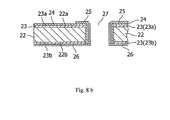
- Fig. 8 is a cross-sectional diagram taken along line A-A of Fig. 7 .
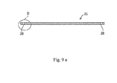
- Fig. 9 is a cross-sectional diagram taken along line B-B of Fig. 7 .
- the conventional thin-film photovoltaic cell 21 has an insulating substrate 22, wherein metal electrode layers 23 are formed on surfaces 22a, 22b of the insulating substrate 22.
- the metal electrode layer 23 on the surface 22a of the insulating substrate 22 functions as a rear electrode layer 23a, and the metal electrode layer 23 on the surface 22b of the insulating substrate 22 as a first back electrode layer 23b.
- a photoelectric conversion layer 24 and a transparent electrode layer 25 are stacked on the rear electrode layer 23a in this order.
- a second back electrode layer 26 is stacked on the first back electrode layer 23b.
- the insulating substrate 22 is provided with first through-holes 27 penetrating through the insulating substrate 22.
- the transparent electrode layer 25 and the second back electrode layer 26 are electrically connected to each other by the first through-holes 27.
- the insulating substrate 22 is provided with second through-holes 28 penetrating through the insulating substrate 22.
- the rear electrode layer 23a and the first back electrode layer 23b are electrically connected to each other by the second through-holes 28.
- the layers stacked on the surface 22a of the insulating substrate 22 are divided by first patterning lines 29, and the layers stacked on the surface 22b of the insulating substrate 22 by second patterning lines 30 (see Fig. 9(b) ). Consequently, the layers stacked on the insulating substrate 22 are divided into a plurality of unit cells. In this case, the first and second patterning lines 29 and 30 alternate with each other on the insulating substrate 22.
- the unit cells adjacent from each other are connected in series by shifting the positions where the surfaces 22a, 22b of the insulating substrate 22 separate from each other and connecting the electrode layers on the surfaces 22a, 22b of the insulating substrate 22 to each other by the second through-holes 28.
- Patent Document 1 discloses another example of a - conventional thin-film photovoltaic cell.
- a first electrode layer, a photoelectric conversion layer, and a second back electrode layer are stacked on one surface of a film substrate made of electrical insulating resin, and a third electrode layer and fourth electrode layer are stacked on the other side (rear surface) of the film substrate.
- Patent Document 2 discloses yet another example of a thin-film photovoltaic cell.
- a connection hole is sealed with a printed electrode made of a conductive material (see, particularly, the paragraph 0035 and Fig. 27).
- Patent Document 1 Japanese Patent Application Publication No. 2001-298203
- Patent Document 2 Japanese Patent Application Publication No. H6-342924
- the configurations shown in Figs. 7 to 9 have the following problems.
- mask processing using a metal mask is performed in the vicinity of each of the second through-holes 28.
- Use of a metal mask needs to take into consideration the manufacturing conditions for the mask processing and latitude for wrap-around of a film to be formed. For this reason, the area of the metal mask needs to be significantly greater than that of each of the second through-holes 28.
- the vicinity of each of the second through-holes 28 has a part where the transparent electrode layer 25 is not formed, as shown in Fig. 9 (b) , limiting the effective area of the transparent electrode layer 25.
- the structure therefore, needs to secure the effective area of the transparent electrode layer 25.
- the second through-holes 28 are disposed at regular intervals, in consideration of the electrical resistances of the first and second back electrode layers 23b and 26. As a result, regions where the transparent electrode layer 25 cannot be formed are provided at regular intervals on the insulating substrate 22.
- the effective area of the transparent electrode layer 25 decreases proportionally, reducing the output of the thin-film photovoltaic cell 21. Reducing the number of the adjacent second through-holes 28 and increasing the intervals therebetween in order to relatively increase the effective area of the transparent electrode layer 25 increases the distance between the wirings in each unit cell and hence the electrical resistances.
- the transparent electrode layer 25 or the like on the insulating substrate 22 comes into contact with the mask, damaging the transparent electrode layer 25 or the like on the insulating substrate 22.
- any of the layers on the insulating substrate 22 is damaged, leak current or the like increases, increasing the failure rate in manufacturing the thin-film photovoltaic cell 21.
- a problem of the technology disclosed in Patent Document 2 is the increase in leak current caused by insufficient insulation of the connection hole sealed with the conductive material. Moreover, the technology disclosed in Patent Document 2 needs to ensure flatness of the material filling the connection hole.
- the mask processing for forming the transparent electrode layer 25 does not have to be performed, by wrapping the photoelectric conversion layer 24 of the surface 22a of the insulating substrate 22 around the back and performing the mask processing on the second back electrode layer 26 of the surface 22b of the insulating substrate 22. Consequently, it is considered that the effective area can be enlarged.
- the second through-holes 28 are punched (a perforating method) or mechanically fabricated, acute-angled protrusions or the like are formed on the edges of the holes. Therefore, the photoelectric conversion layer 24 is damaged even when the photoelectric conversion layer 24 is formed over the edges of the second through-holes 28.
- the present invention was contrived in view of the circumstances described above, and an object thereof is to provide a thin-film photovoltaic cell and a method for producing the same, the method being capable of increasing the effective area of a transparent electrode layer, increasing the output of the thin-film photovoltaic cell by suppressing increase in wiring resistance, and reducing the failure rate in manufacturing the thin-film photovoltaic cell by ensuring insulation of a second through-hole.
- the present invention provides a thin-film photovoltaic cell, having: an insulating substrate; a rear electrode layer, a photoelectric conversion layer, and a transparent electrode layer stacked in this order on one surface of the insulating substrate; a first back electrode layer and a second back electrode layer stacked in this order on the other surface of the insulating substrate; patterning lines that are formed alternately on the layers stacked on both surfaces of the insulating substrate, thereby dividing the insulating substrate into a plurality of unit cells; a first through-hole that penetrates through the insulating substrate to electrically connect the transparent electrode layer and the second back electrode layer to each other; and a second through-hole that penetrates through the insulating substrate to electrically connect the rear electrode layer and the first back electrode layer to each other, the unit cells adjacent to each other being connected in series, wherein the transparent electrode layer around the second through-hole is removed, and the transparent electrode layer and the second back electrode layer are electrically insulated from each other at the second through
- the transparent electrode layer around the second through-hole is removed by sandblasting.
- the patterning lines that are disposed alternately are formed into straight lines and extend in a direction parallel to a width direction of the insulating substrate.
- a plurality of the second through-holes are disposed at equal intervals between the patterning lines that are disposed alternately.
- a distance between an end part of the insulating substrate in the width direction and a center of the second through-hole closest to the end part is half the interval between the second through-holes.
- a distance between the center of the second through-hole and either one of the patterning lines is equal to a distance between the center of the second through-hole and another patterning line.
- the patterning lines that are disposed alternately are formed into straight lines and extend in a direction parallel to a width direction of the insulating substrate.
- the second through-hole is disposed singly between the patterning lines that are disposed alternately.
- a distance between a center of the second through-hole and one end part of the insulating substrate in the width direction is equal to a distance between the center of the second through-hole and the other end part of the insulating substrate in the width direction.
- a distance between the center of the second through-hole and either one of the patterning lines is equal to a distance between the center of the second through-hole and another patterning line.
- a method for producing a thin-film photovoltaic cell has the steps of: forming a second through-hole in an insulating substrate; forming a rear electrode layer on one surface of the insulating substrate and forming a first back electrode layer on the other surface of the insulating substrate; forming a first through-hole in the insulating substrate after forming the rear electrode layer and the first back electrode layer; stacking a photoelectric conversion layer and a transparent electrode layer on the one surface of the insulating substrate in this order and stacking a second back electrode layer on the other surface of the insulating substrate; forming patterning lines alternately on the layers stacked on both surfaces of the insulating substrate and dividing the insulating substrate into a plurality of unit cells; and removing the transparent electrode layer around the second through-hole and electrically insulating the transparent electrode layer and the second back electrode layer from each other at the second through-hole.
- the step of removing the transparent electrode layer around the second through-hole is performed by sandblasting.
- the step of forming a second through-hole forms a plurality of the second through-holes at equal intervals between positions where the alternating patterning lines are formed.
- the patterning lines are formed into straight lines in a direction parallel to a width direction of the insulating substrate. A distance between an end part of the insulating substrate in the width direction and a center of the second through-hole closest to the end part is half the interval between the second through-holes. A distance between the center of the second through-hole and either one of the patterning lines is equal to a distance between the center of the second through-hole and another patterning line.
- the step of forming a second through-hole forms one second through-hole between positions where the alternating patterning lines are formed.
- the patterning lines are formed into straight lines in a direction parallel to a width direction of the insulating substrate.
- a distance between a center of the second through-hole and one end part of the insulating substrate in the width direction is equal to a distance between the center of the second through-hole and the other end part of the insulating substrate in the width direction.
- a distance between the center of the second through-hole and either one of the patterning lines is equal to a distance between the center of the second through-hole and another patterning line.
- a rear electrode layer, a photoelectric conversion layer, and a transparent electrode layer are stacked on one of surfaces of an insulating substrate in this order, and a first back electrode layer and a second back electrode layer are stacked on the other surface of the insulating substrate in this order.
- the insulating substrate is divided into a plurality of unit cells by forming patterning lines alternately on the layers stacked on both surfaces of the insulating substrate.
- the transparent electrode layer and the second back electrode layer are electrically connected to each other by a first through-hole penetrating through the insulating substrate.
- the rear electrode layer and the first back electrode layer are electrically connected to each other by a second through-hole penetrating through the insulating substrate.
- the unit cells adjacent to each other are connected in series.
- the transparent electrode layer around the second through-hole is removed, and the transparent electrode layer and the second back electrode layer are electrically insulated from each other at the second through-hole. For this reason, insulation between the transparent electrode layer and the second back electrode layer can be ensured at the second through-hole, without performing mask processing on the periphery of the second through-hole, unlike the conventional technologies.
- the transparent electrode layer is removed. Therefore, compared to when performing the mask processing, the area of a region without the transparent electrode layer can be reduced, increasing the effective area of the transparent electrode layer. As a result, the output of the thin-film photovoltaic cell can be increased.
- the patterning lines alternating with each other are formed into straight lines and extend in a direction parallel to a width direction of the insulating substrate.
- a plurality of the second through-holes are disposed at equal intervals between the patterning lines alternating with each other.
- the distance between an end part of the insulating substrate in the width direction and the center of the second through-hole closest to the end part is half the interval of the second through-holes.
- the distance between the center of the second through-hole and one of the patterning lines is equal to the distance between the center of the second through-hole and the other patterning line.
- the area of a region without the transparent electrode layer is smaller than that obtained as a result of the mask processing.
- the plurality of second through-holes can be disposed at intervals shorter than those obtained in the conventional technologies. Therefore, the distance between the wirings in each unit cell becomes short. Furthermore, the concentration of current in the second through-holes can be efficiently dispersed, preventing a voltage drop and loss of the output of the thin-film photovoltaic cell. Moreover, even when the plurality of second through-holes are provided in a single unit cell, the output of the thin-film photovoltaic cell can be made higher than those in the conventional technologies.
- the patterning lines alternating with each other are formed into straight lines and extend in a direction parallel to a width direction of the insulating substrate.
- the second through-hole is disposed singly between the patterning lines alternating with each other.
- the distance between the center of the second through-hole and one of end parts of the insulating substrate in the width direction is equal to the distance between the center of the second through-hole and the other end part of the insulating substrate in the width direction.
- the distance between the center of the second through-hole and one of the patterning lines is equal to the distance between the center of the second through-hole and the other patterning line.
- the present invention is particularly useful in a thin-film photovoltaic cell in which the width direction of the insulating substrate is short and a plurality of cells are disposed in the width direction of the insulating substrate.
- the effective area of the transparent electrode layer can be increased by simply removing the transparent electrode layer around the second through-hole.
- the method for producing a thin-film photovoltaic cell according to the present invention includes the steps of: forming a second through-hole in an insulating substrate; forming a rear electrode layer on one surface of the insulating substrate and forming a first back electrode layer on the other surface of the insulating substrate; forming a first through-hole in the insulating substrate after forming the rear electrode layer and the first back electrode layer; stacking a photoelectric conversion layer and a transparent electrode layer on the one surface of the insulating substrate in this order and stacking a second back electrode layer on the other surface of the insulating substrate; forming patterning lines alternately on the layers stacked on both surfaces of the insulating substrate and dividing the insulating substrate into a plurality of unit cells; and removing the transparent electrode layer around the second through-hole and electrically insulating the transparent electrode layer and the second back electrode layer from each other at the second through-hole.
- the transparent electrode layer and the second back electrode layer at the second through-hole without performing the mask processing on the periphery of the second through-hole as in the conventional technologies.
- the transparent electrode layer is simply removed without performing the mask processing on the periphery of the second through-hole, the area of a region without the transparent electrode layer is smaller than that obtained as a result of the mask processing. Consequently, the effective area of the transparent electrode layer can be increased. As a result, the output of the thin-film photovoltaic cell can be increased.
- the mask processing does not have to be performed in the vicinity of the second through-hole, the layers on the insulating substrate can be prevented from being damaged by contact between the mask and the layers on the insulating substrate. Consequently, increase in leak current can be prevented, lowering the failure rate in manufacturing the thin-film photovoltaic cell.
- the step of removing the transparent electrode layer around the second through-hole is performed by sandblasting, thereby enabling the periphery of the second through-hole to be precisely processed.
- the step of forming the second through-hole forms a plurality of the second through-holes at equal intervals between positions where the alternating pattern lines are formed.
- the patterning lines are formed into straight lines in a direction parallel to a width direction of the insulating substrate.
- the distance between an end part of the insulating substrate in the width direction and the center of the second through-hole closest to the end part is half the interval of the second through-holes.
- the distance between the center of the second through-hole and one of the patterning lines is equal to the distance between the center of the second through-hole and the other patterning line.
- the area of a region without the transparent electrode layer is smaller than that obtained as a result of the mask processing.
- the plurality of second through-holes can be disposed at intervals shorter than those obtained in the conventional technologies. Therefore, the distance between the wirings in each unit cell becomes short. Furthermore, the concentration of current in the second through-holes can be efficiently dispersed, preventing loss of the output of the thin-film photovoltaic cell. Moreover, even when the plurality of second through-holes are provided in a single unit cell, the output of the thin-film photovoltaic cell can be made higher than those in the conventional technologies.
- the step of forming the second through-hole forms a single second through-hole between the positions where the alternating patterning lines are formed.
- the patterning lines alternating with each other are formed into straight lines in a direction parallel to the width direction of the insulating substrate.
- the distance between the center of the second through-hole and one of end parts of the insulating substrate in the width direction is equal to the distance between the center of the second through-hole and the other end part of the insulating substrate in the width direction.
- the distance between the center of the second through-hole and one of the patterning lines is equal to the distance between the center of the second through-hole and the other patterning line.
- the present invention is particularly useful in a thin-film photovoltaic cell in which the width direction of the insulating substrate is short and a plurality of cells are disposed in the width direction of the insulating substrate.
- the effective area of the transparent electrode layer can be increased by simply removing the transparent electrode layer around the second through-hole.
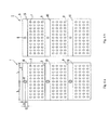
- Figs. 1(a) and 1(b) are plan views of a thin-film photovoltaic cell according to a first embodiment of the present invention, Fig. 1(a) being a plan view showing the thin-film photovoltaic cell from the rear electrode layer side and Fig. 1(b) a plan view showing the thin-film photovoltaic cell from the first and second back electrode layers side;
- Fig. 1 is a plan view of a thin-film photovoltaic cell according to a first embodiment.
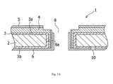
- Fig. 2 is a cross-sectional diagram taken along line A-A of Fig. 1 .
- Fig. 3 is a cross-sectional diagram taken along line B-B of Fig. 1 .
- a thin-film photovoltaic cell 1 has an insulating substrate 2.
- the insulating substrate 2 is formed from a film material of, for example, polyimide, polyamideimide, polyethylenenaphthalate, or aramid.
- a metal electrode layer 3 containing metal is formed on either surface 2a, 2b of the insulating substrate 2.
- the metal electrode layer 3 on the surface 2a of the insulating substrate 2 functions as a rear electrode layer 3a, and the metal electrode layer 3 on the surface 2b of the insulating substrate 2 as a first back electrode layer 3b.
- a photoelectric conversion layer 4 and a transparent electrode layer 5 are stacked, in this order, on the rear electrode layer 3a on the surface 2a of the insulating substrate 2.
- An amorphous semiconductor, amorphous compound conductor, dye-sensitized photovoltaic cell, or CIGS organic photovoltaic cell can be used s the photoelectric conversion layer 4.
- a second back electrode layer 6 is stacked on the first back electrode layer 3b on the surface 2b of the insulating substrate 2.
- the insulating substrate 2 is provided with first through-holes 7 penetrating through the insulating substrate 2.
- the transparent electrode layer 5 and the second back electrode layer 6 are connected to each other so as to overlap on each other at side wall parts 7a of the first through-holes 7.
- the insulating substrate 2 is provided with second through-holes 8 penetrating through the insulating substrate 2.
- the second through-holes 8 are formed in pairs at equal intervals at either end part of the insulating substrate 2 of the thin-film photovoltaic cell 1 in a width direction of the insulating substrate 2. Furthermore, as shown in Fig.
- the rear electrode layer 3a and the first back electrode layer 3b are electrically connected to each other by side wall parts 8a of the second through-holes 8.
- the first and second through-holes 7 and 8 are used for connecting the first and second back electrode layers 3b and 6, the first through-holes 7, the transparent electrode layer 5, the photoelectric conversion layer 4, the rear electrode layer 3a, the second through-holes 8, and the first back electrode layer 3b, in this order.
- the layers stacked on the surface 2a of the insulating substrate 2 are laser-processed and thereby divided into a plurality of pieces by first patterning lines 9.
- the layers stacked on the surface 2b of the insulating substrate 2 are laser-processed and thereby divided into a plurality of pieces by second patterning lines 10.
- the first patterning lines 9 and the second patterning lines 10 alternate with each other in the insulating substrate 2.
- the insulating substrate 2 is divided into unit cells (unit photovoltaic cells) formed of the layers stacked on the surfaces 2a and 2b of the insulating substrate 2 by the first and second patterning lines 9 and 10.
- unit cells unit photovoltaic cells
- the positions where the electrode layers on the surfaces 2a and 2b of the insulating substrate 2 are separated are shifted, and the electrode layers on the surfaces 2a and 2b of the insulating substrate 2 are connected to one another by second through-holes 28, so that the unit cells adjacent to each other are connected in series.
- the second patterning lines 10 where the layers on the back of the insulating substrate 2 are removed are bent. Specifically, in the present embodiment, each of the second patterning lines 10 is bent 90° twice.
- a unit photoelectric conversion part and unit rear electrode layer constituting each unit cell are substantially aligned, with the insulating substrate 2 therebetween. Therefore, with no limitations on the positions for forming the first through-holes 7 in each unit cell (without forming the first through-holes 7 in an unbalanced manner), a desired number of first through-holes 7 can be formed in desired positions in accordance with a condition for producing the thin-film photovoltaic cell, improving current collection efficiency.
- the shape of the second patterning lines 10 may not only be the shape illustrated in the present embodiment but also be a shape including a curve, such an obliquely bent structure. Furthermore, the second patterning lines 10 may be straight lines, whereas the first patterning lines 9 have bent parts. Or, both the first patterning lines 9 and the second patterning lines 10 may have bent parts.
- the present embodiment is characterized in that the periphery of each second through-hole 8 is processed in order to partially remove the transparent electrode layer 5 around each second through-holes 8, as shown in Fig. 3(b) . Therefore, the transparent electrode layer 5 and the second back electrode layer 6 are electrically connected to each other at the second through-holes 8. Consequently, the transparent electrode layer 5 and the first back electrode layer 3b are electrically insulated from each other at the second through-holes 8. In terms of performing precision fabrication on the periphery of each second through-hole 8, it is effective to sandblast the periphery of each second through-hole 8.
- the method for fabricating the periphery of each second through-hole 8 is not limited to sandblasting as long as the properties of the thin-film photovoltaic cell 1 are not degraded.
- the method for fabricating may be able to perform counterboring without causing thermal denaturation in the photoelectric conversion layer 4 and includes, for example, cutting, dry etching, and wet etching.
- the fabrication range can be determined by spraying sand locally without using a mask.
- the film material described is used as the insulating substrate 2.
- a roll-to-roll printing process or an inkj et printing technique is used as a method for producing the thin-film photovoltaic cell 1.
- the roll-to-roll printing process conveys substrates made from a film material by using a plurality of rollers (conveying means) and continuously forms thin films on the substrates in film-forming chambers that are disposed continuously.
- Fig. 4 is a flowchart of a procedure for producing the thin-film photovoltaic cell 1 according to the present embodiment.
- the insulating substrate 2 is pretreated in step S1, as shown in Fig. 4 . More specifically, when pretreating the insulating substrate 2, the insulating substrate 2 is exposed to a plasma to cleanse the surfaces thereof.
- the second through-holes 8 are formed in the insulating substrate 2.
- the second through-holes 8 are punched (a perforating method).
- the shape of each second through-hole 8 is a circular shape with a diameter of 1 mm.
- the diameter of each circular second through-hole 8 is set within a range of 0.05 to 1 mm.
- the second through-holes 8 are formed in pairs at equal intervals at either end part of the insulating substrate 2 of the thin-film photovoltaic cell 1 in the width direction of the insulating substrate 2. Note that the number of second through-holes 8 to be punched can be adjusted depending on the design.
- step S3 sputtering is performed to form the rear electrode layer 3a and the first back electrode layer 3b on the surfaces 2a and 2b of the insulating substrate 2, respectively.
- the rear electrode layer 3a and the first back electrode layer 3b are electrically connected to each other by the second through-holes 8.
- step S4 the layers formed on the surfaces 2a and 2b of the insulating substrate 2 are laser-processed and removed to form primary patterning lines (not shown). In so doing, the lines formed on the surfaces 2a and 2b of the insulating substrate 2 are disposed alternately.
- step S5 the first through-holes 7 are formed in the insulating substrate 2. The first through-holes 7 are punched.
- the insulating substrate 2 is heated to a certain temperature or higher that is used in a subsequent step (step S6 for forming the photoelectric conversion layer 4, the transparent electrode layer 5, and the like). Specifically, the insulating substrate 2 is heated to 250°C or higher, or preferably 300°C or higher. This can prevent the layers formed in the subsequent steps from peeling off.
- step S6 the photoelectric conversion layer 4 is formed on the rear electrode layer 3a of the insulating substrate 2. Thereafter in step S7, the transparent electrode layer 5 is formed on the photoelectric conversion layer 4. In the subsequent step S8, the second back electrode layer 6 is formed on the first back electrode layer 3b of the insulating substrate 2.
- step S9 the photoelectric conversion layer 4 and the transparent electrode layer 5 on the primary patterning lines formed in step S4 are laser-processed and removed again, to form the first patterning lines 9.
- step S10 the second back electrode layer 6 on the primary patterning line formed in step S4 is laser-processed and removed again, to form the second patterning lines 10.
- the layers on the insulating substrate 2 are separated into a plurality of unit cells by the first and second patterning lines 9 and 10.
- each second through-hole 8 is sandblasted to remove a conductive film including the transparent electrode layer 5.
- the second back electrode layer 6 is removed as well because the second back electrode layer 6 might be wrapped around on the transparent electrode layer 5.
- a counterbore diameter which is larger than the diameter of each second through-hole 8 by approximately 0.1 to 1 mm, is formed around each second through-hole 8. The fabrication is performed to the level as deep as the middle of the photoelectric conversion layer 4 so as to keep the photoelectric conversion layer 4.
- This fabrication may scrape off the photoelectric conversion layer 4 completely, but it is preferred that the rear electrode layer 3a be kept entirely without being damaged as much as possible, so that the resistances do not increase. In this manner the series connection of the thin-film photovoltaic cell 1 is completed.
- the rear electrode layer 3a, the photoelectric conversion layer 4, and the transparent electrode layer 5 are stacked, in this order, on the surface 2a of the insulating substrate 2, and the first back electrode layer 3b and the second back electrode layer 6 are stacked, in this order, on the surface 2b of the insulating substrate 2.
- the first and second patterning lines 9 and 10 are formed alternately on the layers stacked on the surfaces 2a and 2b of the insulating substrate 2, thereby dividing the insulating substrate 2 into a plurality of unit cells.
- the transparent electrode layer 5 and the second back electrode layer 6 are electrically connected to each other by the first through-holes 7 penetrating through the insulating substrate 2.
- the rear electrode layer 3a and the first back electrode layer 3b are electrically connected to each other by the second through-holes 8 penetrating through the insulating substrate 2.
- the unit cells adj acent to each other are connected in series.
- the transparent electrode layer 5 around each of the second through-holes 8 is removed, and the transparent electrode layer 5 and the second back electrode layer 6 are electrically insulated from each other at the second through-holes 8. Therefore, without performing the mask processing around the second through-holes as in the conventional technologies, insulation between the transparent electrode layer 5 and the second back electrode layer 6 can be ensured at the second through-holes 8.
- the transparent electrode layer 5 is simply removed without performing the mask processing on the periphery of each of the second through-holes 8, the area of a region without the transparent electrode layer 5 is smaller than that obtained as a result of the mask processing.
- the effective area of the transparent electrode layer 5 can be made wider than those of the conventional technologies. As a result, the output of the thin-film photovoltaic cell 1 can be increased.
- the method for producing the thin-film photovoltaic cell 1 according to the first embodiment of the present invention includes the steps of: forming the second through-holes 8 in the insulating substrate 2; forming the rear electrode layer 3a on the surface 2a of the insulating substrate 2 and forming the first back electrode layer 3b on the surface 2b of the insulating substrate 2; forming the first through-holes 7 in the insulating substrate 2 after forming the rear electrode layer 3a and the first back electrode layer 3b; stacking the photoelectric conversion layer 4 and the transparent electrode layer 5 on the surface 2a of the insulating substrate 2 in this order and stacking the second back electrode layer 6 on the surface 2b of the insulating substrate 2; forming the first and second patterning lines 9 and 10 alternately on the layers stacked on the surfaces 2a and 2b of the insulating substrate 2 and dividing the insulating substrate 2 into a plurality of unit cells; and removing the transparent electrode layer 5 around the second through-holes 8 and electrically insulating the transparent electrode layer 5 and the
- the mask processing does not have to be performed in the vicinity of the second through-holes, improving the yield of production of the thin-film photovoltaic cell 1.
- the layers on the insulating substrate 2 can be prevented from being damaged by contact between the mask and the layers on the insulating substrate 2. Consequently, increase in leak current in the thin-film photovoltaic cell 1 can be prevented, lowering the failure rate in manufacturing the thin-film photovoltaic cell 1.
- Figs. 5(a) and 5(b) are plan views of the thin-film photovoltaic cell according to the second embodiment, Fig. 5(a) being a plan view showing the thin-film photovoltaic cell from the rear electrode layer side and Fig. 5(b) a plan view showing the thin-film photovoltaic cell from the first and second back electrode layers side. Note that the same reference numerals are applied to the sections same as those described in the above embodiment. Therefore, the overlapping descriptions are omitted.
- the first patterning lines 9 and the second patterning lines 10 are formed into straight lines and extend in a direction parallel to the width direction of the insulating substrate 2, as shown in Fig. 5 .
- a plurality of second through-holes 8 are disposed in a line between the alternating first and second patterning lines 9 and 10.
- the plurality of second through-holes 8 are disposed at an interval of d 1 .
- a distance d 2 between an end part of the insulating substrate 2 in the width direction and the center of the second through-hole 8 closest to this end part is half the interval d 1 of the second through-holes.
- a region around each second through-hole 8 where the transparent electrode layer 5 is not formed falls within a range between each first patterning line 9 and each second patterning line 10 that alternate with each other. Moreover, a distance S 1 between the center of the second through-hole 8 and the first patterning line 9 is equal to a distance S 2 between the center of the second through-hole 8 and the second patterning line 10.
- the concentration of current in the second through-holes 8 can be dispersed, preventing the loss of the output of the thin-film photovoltaic cell 1.
- the output of the thin-film photovoltaic cell 1 can be made higher than those in the conventional technologies. Additionally, the distance between the wirings and the thickness of the wiring materials can be made reduced, accomplishing cost reduction.
- Figs. 6(a) and 6(b) are plan views of the thin-film photovoltaic cell according to the third embodiment of the present invention, Fig. 6 (a) being a plan view showing the thin-film photovoltaic cell from the rear electrode layer side and Fig. 6(b) a plan view showing the' thin-film photovoltaic cell from the first and second back electrode layers side. Note that the same reference numerals are applied to the sections same as those described in the above embodiment. Therefore, the overlapping descriptions are omitted.
- the first patterning lines 9 and the second patterning lines 10 are formed into straight lines and extend in a direction parallel to the width direction of the insulating substrate 2, as shown in Fig. 6 . Also, only one second through-hole 8 is disposed between each of the first patterning lines 9 and each of the second patterning lines 10, the first and second patterning lines 9 and 10 being disposed alternately.
- a distance l 1 between the center of the second through-hole 8 and one of end parts of the insulating substrate 2 in the width direction is equal to a distance l 2 between the center of the second through-hole 8 and the other end part of the insulating substrate 2 in the width direction.
- a distance S 1 between the center of the second through-hole 8 and the first patterning line 9 is equal to a distance S 2 between the center of the second through-hole 8 and the second patterning line 10.
- the thin-film photovoltaic cell 1 of the third embodiment is particularly useful in a thin-film photovoltaic cell in which the width direction of the insulating substrate 2 is short and a plurality of cells are disposed in the width direction of the insulating substrate 2.
- the effective area of the transparent electrode layer 5 can be increased by simply removing the transparent electrode layer 5 around the second through-hole 8.
- disposing the plurality of cells in the width direction of the insulating substrate 2 can prevent the increase of the electrical resistances of the first and second back electrode layers 3b and 6.
- step S11 the step of removing the conductive film including the transparent electrode layer 5 (S11) is executed at the end.
- step S11 can be executed any time after step S8.
Landscapes
- Photovoltaic Devices (AREA)
- Life Sciences & Earth Sciences (AREA)
- Engineering & Computer Science (AREA)
- Sustainable Development (AREA)
- Sustainable Energy (AREA)
Abstract
In a thin-film photovoltaic cell 1 of the present invention, a rear electrode layer 3a, a photoelectric conversion layer 4, and a transparent electrode layer 5 are stacked in this order on a surface 2a of an insulating substrate 2, and a first back electrode layer 3b and a second back electrode layer 6 are stacked in this order on a surface 2b of the insulating substrate 2. The transparent electrode layer 5 and the second back electrode layer 6 are electrically connected to each other by a first through-hole 7 that penetrates through the insulating substrate 2. The rear electrode layer 3a and the first back electrode layer 3b are electrically connected to each other by a second through-hole 8 that penetrates through the insulating substrate 2. The transparent electrode layer 5 around the second through-hole 8 is removed, and the transparent electrode layer 5 and the second back electrode layer 6 are electrically insulated from each other at the second through-hole 8.
Description
- The present invention relates to a thin-film photovoltaic cell formed by stacking a metal electrode layer, a photoelectric conversion layer, and a transparent electrode layer on a film substrate.
-
Fig. 7 is a plan view of a conventional thin-film photovoltaic cell.Fig. 8 is a cross-sectional diagram taken along line A-A ofFig. 7 .Fig. 9 is a cross-sectional diagram taken along line B-B ofFig. 7 .
As shown inFigs. 8 and9 , the conventional thin-filmphotovoltaic cell 21 has aninsulating substrate 22, whereinmetal electrode layers 23 are formed onsurfaces insulating substrate 22. Themetal electrode layer 23 on thesurface 22a of theinsulating substrate 22 functions as arear electrode layer 23a, and themetal electrode layer 23 on thesurface 22b of theinsulating substrate 22 as a firstback electrode layer 23b. - Also, as shown in
Figs. 8 and9 , aphotoelectric conversion layer 24 and atransparent electrode layer 25 are stacked on therear electrode layer 23a in this order. A secondback electrode layer 26 is stacked on the firstback electrode layer 23b.
As shown inFigs. 7 and8 , theinsulating substrate 22 is provided with first through-holes 27 penetrating through theinsulating substrate 22. Thetransparent electrode layer 25 and the secondback electrode layer 26 are electrically connected to each other by the first through-holes 27. Furthermore, as shown inFigs. 7 and9 , theinsulating substrate 22 is provided with second through-holes 28 penetrating through theinsulating substrate 22. Therear electrode layer 23a and the firstback electrode layer 23b are electrically connected to each other by the second through-holes 28. - As shown in
Fig. 7 , the layers stacked on thesurface 22a of theinsulating substrate 22 are divided byfirst patterning lines 29, and the layers stacked on thesurface 22b of theinsulating substrate 22 by second patterning lines 30 (seeFig. 9(b) ). Consequently, the layers stacked on theinsulating substrate 22 are divided into a plurality of unit cells.
In this case, the first andsecond patterning lines insulating substrate 22. The unit cells adjacent from each other are connected in series by shifting the positions where thesurfaces insulating substrate 22 separate from each other and connecting the electrode layers on thesurfaces insulating substrate 22 to each other by the second through-holes 28. -
Patent Document 1 discloses another example of a - conventional thin-film photovoltaic cell. In the thin-film photovoltaic cell ofPatent Document 1, a first electrode layer, a photoelectric conversion layer, and a second back electrode layer are stacked on one surface of a film substrate made of electrical insulating resin, and a third electrode layer and fourth electrode layer are stacked on the other side (rear surface) of the film substrate. -
Patent Document 2 discloses yet another example of a thin-film photovoltaic cell. In the thin-film photovoltaic cell ofPatent Document 2, a connection hole is sealed with a printed electrode made of a conductive material (see, particularly, the paragraph 0035 and Fig. 27). - Patent Document 1: Japanese Patent Application Publication No.
2001-298203
Patent Document 2: Japanese Patent Application Publication No.H6-342924 - Unfortunately, the configurations shown in
Figs. 7 to 9 have the following problems.
In the conventional structure, when forming thetransparent electrode layer 26 in order to prevent thetransparent electrode layer 25 and the secondback electrode layer 26 from coming into contact with each other at the second through-holes 28, mask processing using a metal mask is performed in the vicinity of each of the second through-holes 28. Use of a metal mask needs to take into consideration the manufacturing conditions for the mask processing and latitude for wrap-around of a film to be formed. For this reason, the area of the metal mask needs to be significantly greater than that of each of the second through-holes 28. Thus, the vicinity of each of the second through-holes 28 has a part where thetransparent electrode layer 25 is not formed, as shown inFig. 9 (b) , limiting the effective area of thetransparent electrode layer 25.
The structure, therefore, needs to secure the effective area of thetransparent electrode layer 25. - When forming a plurality of the second through-
holes 28 per unit cell, the second through-holes 28 are disposed at regular intervals, in consideration of the electrical resistances of the first and secondback electrode layers transparent electrode layer 25 cannot be formed are provided at regular intervals on theinsulating substrate 22. When the number of the second through-holes 28 is increased, the effective area of thetransparent electrode layer 25 decreases proportionally, reducing the output of the thin-filmphotovoltaic cell 21.
Reducing the number of the adjacent second through-holes 28 and increasing the intervals therebetween in order to relatively increase the effective area of thetransparent electrode layer 25 increases the distance between the wirings in each unit cell and hence the electrical resistances. In addition, more current concentrates on a single second through-hole. This results in a further voltage drop and loss of the output of the thin-film photovoltaic cell.
Therefore, a structure that prevents concentration of current in the second through-holes 28 and increase of the electrical resistances while securing the effective area of the transparent electrode layer is required. - When performing the mask processing in the vicinity of each of the second through-
holes 28, thetransparent electrode layer 25 or the like on theinsulating substrate 22 comes into contact with the mask, damaging thetransparent electrode layer 25 or the like on theinsulating substrate 22. When any of the layers on theinsulating substrate 22 is damaged, leak current or the like increases, increasing the failure rate in manufacturing the thin-filmphotovoltaic cell 21. - A problem of the technology disclosed in
Patent Document 2 is the increase in leak current caused by insufficient insulation of the connection hole sealed with the conductive material. Moreover, the technology disclosed inPatent Document 2 needs to ensure flatness of the material filling the connection hole. - The mask processing for forming the
transparent electrode layer 25 does not have to be performed, by wrapping thephotoelectric conversion layer 24 of thesurface 22a of theinsulating substrate 22 around the back and performing the mask processing on the secondback electrode layer 26 of thesurface 22b of theinsulating substrate 22. Consequently, it is considered that the effective area can be enlarged.
However, because the second through-holes 28 are punched (a perforating method) or mechanically fabricated, acute-angled protrusions or the like are formed on the edges of the holes. Therefore, thephotoelectric conversion layer 24 is damaged even when thephotoelectric conversion layer 24 is formed over the edges of the second through-holes 28. Especially when thephotoelectric conversion layer 24 is damaged, leak current occurs between thetransparent electrode layer 26 and therear electrode layer 23a due to a large potential difference therebetween.
Even when the mask processing is performed on the secondback electrode layer 26 instead of on thetransparent electrode layer 25, leak current or the like increases, increasing the failure rate in manufacturing the thin-filmphotovoltaic cell 21. - The present invention was contrived in view of the circumstances described above, and an object thereof is to provide a thin-film photovoltaic cell and a method for producing the same, the method being capable of increasing the effective area of a transparent electrode layer, increasing the output of the thin-film photovoltaic cell by suppressing increase in wiring resistance, and reducing the failure rate in manufacturing the thin-film photovoltaic cell by ensuring insulation of a second through-hole.
- In order to solve the problems of the conventional technologies, the present invention provides a thin-film photovoltaic cell, having: an insulating substrate; a rear electrode layer, a photoelectric conversion layer, and a transparent electrode layer stacked in this order on one surface of the insulating substrate; a first back electrode layer and a second back electrode layer stacked in this order on the other surface of the insulating substrate; patterning lines that are formed alternately on the layers stacked on both surfaces of the insulating substrate, thereby dividing the insulating substrate into a plurality of unit cells; a first through-hole that penetrates through the insulating substrate to electrically connect the transparent electrode layer and the second back electrode layer to each other; and a second through-hole that penetrates through the insulating substrate to electrically connect the rear electrode layer and the first back electrode layer to each other, the unit cells adjacent to each other being connected in series, wherein the transparent electrode layer around the second through-hole is removed, and the transparent electrode layer and the second back electrode layer are electrically insulated from each other at the second through-hole.
- According to the thin-film photovoltaic cell of the present invention, the transparent electrode layer around the second through-hole is removed by sandblasting.
- According to the thin-film photovoltaic cell of the present invention, the patterning lines that are disposed alternately are formed into straight lines and extend in a direction parallel to a width direction of the insulating substrate. A plurality of the second through-holes are disposed at equal intervals between the patterning lines that are disposed alternately. A distance between an end part of the insulating substrate in the width direction and a center of the second through-hole closest to the end part is half the interval between the second through-holes. A distance between the center of the second through-hole and either one of the patterning lines is equal to a distance between the center of the second through-hole and another patterning line.
- According to the thin-film photovoltaic cell of the present invention, the patterning lines that are disposed alternately are formed into straight lines and extend in a direction parallel to a width direction of the insulating substrate. The second through-hole is disposed singly between the patterning lines that are disposed alternately. A distance between a center of the second through-hole and one end part of the insulating substrate in the width direction is equal to a distance between the center of the second through-hole and the other end part of the insulating substrate in the width direction. A distance between the center of the second through-hole and either one of the patterning lines is equal to a distance between the center of the second through-hole and another patterning line.
- In order to solve the problems of the conventional technologies, a method for producing a thin-film photovoltaic cell according to the present invention has the steps of: forming a second through-hole in an insulating substrate; forming a rear electrode layer on one surface of the insulating substrate and forming a first back electrode layer on the other surface of the insulating substrate; forming a first through-hole in the insulating substrate after forming the rear electrode layer and the first back electrode layer; stacking a photoelectric conversion layer and a transparent electrode layer on the one surface of the insulating substrate in this order and stacking a second back electrode layer on the other surface of the insulating substrate; forming patterning lines alternately on the layers stacked on both surfaces of the insulating substrate and dividing the insulating substrate into a plurality of unit cells; and removing the transparent electrode layer around the second through-hole and electrically insulating the transparent electrode layer and the second back electrode layer from each other at the second through-hole.
- In the method for forming a thin-film photovoltaic cell according to the present invention, the step of removing the transparent electrode layer around the second through-hole is performed by sandblasting.
- In the method for producing a thin-film photovoltaic cell according to the present invention, the step of forming a second through-hole forms a plurality of the second through-holes at equal intervals between positions where the alternating patterning lines are formed. The patterning lines are formed into straight lines in a direction parallel to a width direction of the insulating substrate. A distance between an end part of the insulating substrate in the width direction and a center of the second through-hole closest to the end part is half the interval between the second through-holes. A distance between the center of the second through-hole and either one of the patterning lines is equal to a distance between the center of the second through-hole and another patterning line.
- In the method for producing a thin-film photovoltaic cell according to the present invention, the step of forming a second through-hole forms one second through-hole between positions where the alternating patterning lines are formed. The patterning lines are formed into straight lines in a direction parallel to a width direction of the insulating substrate. A distance between a center of the second through-hole and one end part of the insulating substrate in the width direction is equal to a distance between the center of the second through-hole and the other end part of the insulating substrate in the width direction. A distance between the center of the second through-hole and either one of the patterning lines is equal to a distance between the center of the second through-hole and another patterning line.
- In the thin-film photovoltaic cell according to the present invention, a rear electrode layer, a photoelectric conversion layer, and a transparent electrode layer are stacked on one of surfaces of an insulating substrate in this order, and a first back electrode layer and a second back electrode layer are stacked on the other surface of the insulating substrate in this order. The insulating substrate is divided into a plurality of unit cells by forming patterning lines alternately on the layers stacked on both surfaces of the insulating substrate. The transparent electrode layer and the second back electrode layer are electrically connected to each other by a first through-hole penetrating through the insulating substrate. The rear electrode layer and the first back electrode layer are electrically connected to each other by a second through-hole penetrating through the insulating substrate. The unit cells adjacent to each other are connected in series. The transparent electrode layer around the second through-hole is removed, and the transparent electrode layer and the second back electrode layer are electrically insulated from each other at the second through-hole. For this reason, insulation between the transparent electrode layer and the second back electrode layer can be ensured at the second through-hole, without performing mask processing on the periphery of the second through-hole, unlike the conventional technologies. Moreover, instead of performing the mask processing on the periphery of the second through-hole, the transparent electrode layer is removed. Therefore, compared to when performing the mask processing, the area of a region without the transparent electrode layer can be reduced, increasing the effective area of the transparent electrode layer. As a result, the output of the thin-film photovoltaic cell can be increased.
- In the thin-film photovoltaic cell according to the present invention, the patterning lines alternating with each other are formed into straight lines and extend in a direction parallel to a width direction of the insulating substrate. A plurality of the second through-holes are disposed at equal intervals between the patterning lines alternating with each other. The distance between an end part of the insulating substrate in the width direction and the center of the second through-hole closest to the end part is half the interval of the second through-holes. The distance between the center of the second through-hole and one of the patterning lines is equal to the distance between the center of the second through-hole and the other patterning line. According to the present invention, the area of a region without the transparent electrode layer is smaller than that obtained as a result of the mask processing. For this reason, the plurality of second through-holes can be disposed at intervals shorter than those obtained in the conventional technologies. Therefore, the distance between the wirings in each unit cell becomes short. Furthermore, the concentration of current in the second through-holes can be efficiently dispersed, preventing a voltage drop and loss of the output of the thin-film photovoltaic cell. Moreover, even when the plurality of second through-holes are provided in a single unit cell, the output of the thin-film photovoltaic cell can be made higher than those in the conventional technologies.
- In the thin-film photovoltaic cell according to the present invention, the patterning lines alternating with each other are formed into straight lines and extend in a direction parallel to a width direction of the insulating substrate. The second through-hole is disposed singly between the patterning lines alternating with each other. The distance between the center of the second through-hole and one of end parts of the insulating substrate in the width direction is equal to the distance between the center of the second through-hole and the other end part of the insulating substrate in the width direction. The distance between the center of the second through-hole and one of the patterning lines is equal to the distance between the center of the second through-hole and the other patterning line. The present invention is particularly useful in a thin-film photovoltaic cell in which the width direction of the insulating substrate is short and a plurality of cells are disposed in the width direction of the insulating substrate. According to the configuration of the present invention, the effective area of the transparent electrode layer can be increased by simply removing the transparent electrode layer around the second through-hole.
- The method for producing a thin-film photovoltaic cell according to the present invention includes the steps of: forming a second through-hole in an insulating substrate; forming a rear electrode layer on one surface of the insulating substrate and forming a first back electrode layer on the other surface of the insulating substrate; forming a first through-hole in the insulating substrate after forming the rear electrode layer and the first back electrode layer; stacking a photoelectric conversion layer and a transparent electrode layer on the one surface of the insulating substrate in this order and stacking a second back electrode layer on the other surface of the insulating substrate; forming patterning lines alternately on the layers stacked on both surfaces of the insulating substrate and dividing the insulating substrate into a plurality of unit cells; and removing the transparent electrode layer around the second through-hole and electrically insulating the transparent electrode layer and the second back electrode layer from each other at the second through-hole. Therefore, insulation can be ensured between the transparent electrode layer and the second back electrode layer at the second through-hole, without performing the mask processing on the periphery of the second through-hole as in the conventional technologies. In addition, because the transparent electrode layer is simply removed without performing the mask processing on the periphery of the second through-hole, the area of a region without the transparent electrode layer is smaller than that obtained as a result of the mask processing. Consequently, the effective area of the transparent electrode layer can be increased. As a result, the output of the thin-film photovoltaic cell can be increased.
Furthermore, because the mask processing does not have to be performed in the vicinity of the second through-hole, the layers on the insulating substrate can be prevented from being damaged by contact between the mask and the layers on the insulating substrate. Consequently, increase in leak current can be prevented, lowering the failure rate in manufacturing the thin-film photovoltaic cell. - According to the method for producing a thin-film photovoltaic cell, the step of removing the transparent electrode layer around the second through-hole is performed by sandblasting, thereby enabling the periphery of the second through-hole to be precisely processed.
- Furthermore, in the method for producing a thin-film photovoltaic cell according to the present invention, the step of forming the second through-hole forms a plurality of the second through-holes at equal intervals between positions where the alternating pattern lines are formed. The patterning lines are formed into straight lines in a direction parallel to a width direction of the insulating substrate. The distance between an end part of the insulating substrate in the width direction and the center of the second through-hole closest to the end part is half the interval of the second through-holes. The distance between the center of the second through-hole and one of the patterning lines is equal to the distance between the center of the second through-hole and the other patterning line. According to the present invention, the area of a region without the transparent electrode layer is smaller than that obtained as a result of the mask processing. For this reason, the plurality of second through-holes can be disposed at intervals shorter than those obtained in the conventional technologies. Therefore, the distance between the wirings in each unit cell becomes short. Furthermore, the concentration of current in the second through-holes can be efficiently dispersed, preventing loss of the output of the thin-film photovoltaic cell. Moreover, even when the plurality of second through-holes are provided in a single unit cell, the output of the thin-film photovoltaic cell can be made higher than those in the conventional technologies.
- In the method for producing a thin-film photovoltaic cell according to the present invention, the step of forming the second through-hole forms a single second through-hole between the positions where the alternating patterning lines are formed. The patterning lines alternating with each other are formed into straight lines in a direction parallel to the width direction of the insulating substrate. The distance between the center of the second through-hole and one of end parts of the insulating substrate in the width direction is equal to the distance between the center of the second through-hole and the other end part of the insulating substrate in the width direction. The distance between the center of the second through-hole and one of the patterning lines is equal to the distance between the center of the second through-hole and the other patterning line. The present invention is particularly useful in a thin-film photovoltaic cell in which the width direction of the insulating substrate is short and a plurality of cells are disposed in the width direction of the insulating substrate. According to the configuration of the present invention, the effective area of the transparent electrode layer can be increased by simply removing the transparent electrode layer around the second through-hole.
-
Figs. 1(a) and 1(b) are plan views of a thin-film photovoltaic cell according to a first embodiment of the present invention,Fig. 1(a) being a plan view showing the thin-film photovoltaic cell from the rear electrode layer side andFig. 1(b) a plan view showing the thin-film photovoltaic cell from the first and second back electrode layers side; -
Fig. 2 is a cross-sectional diagram taken along line A-A ofFig. 1 ; -
Figs. 3(a) and3(b) are cross-sectional diagrams taken along line B-B ofFig. 1 ,Fig. 3(a) being a cross-sectional diagram showing a state prior to removal of a transparent electrode layer andFig. 3 (b) a cross-sectional diagram showing a state after removal of the transparent electrode layer; -
Fig. 4 is a flowchart of a procedure for producing the thin-film photovoltaic cell according to the embodiment of the present invention; -
Figs. 5(a) and 5(b) are plan views of a thin-film photovoltaic cell according to a second embodiment of the present invention,Fig. 5(a) being a plan view showing the thin-film photovoltaic cell from the rear electrode layer side andFig. 5(b) a plan view showing the thin-film photovoltaic cell from the first and second back electrode layers side; -
Figs. 6(a) and 6(b) are plan views of a thin-film photovoltaic cell according to a third embodiment of the present invention,Fig. 6(a) being a plan view showing the thin-film photovoltaic cell from the rear electrode layer side andFig. 6(b) a plan view showing the thin-film photovoltaic cell from the first and second back electrode layers side; -
Fig. 7 is a plan view of a conventional thin-film photovoltaic cell; -
Fig. 8(a) is a cross-sectional diagram taken along line A-A ofFig. 7 , andFig. 8(b) is an enlarged view of section C shown inFig. 8(a) ; and -
Fig. 9 (a) is a cross-sectional diagram taken along a line B-B ofFig. 7 , andFig. 9(b) is an enlarged view of section D shown inFig. 9(a) . - Thin-film photovoltaic cells according to embodiments of the present invention are described hereinafter with reference to the drawings.
Fig. 1 is a plan view of a thin-film photovoltaic cell according to a first embodiment.Fig. 2 is a cross-sectional diagram taken along line A-A ofFig. 1 .Fig. 3 is a cross-sectional diagram taken along line B-B ofFig. 1 . - As shown in
Figs. 1 to 3 , a thin-filmphotovoltaic cell 1 according to the present embodiment has an insulatingsubstrate 2. The insulatingsubstrate 2 is formed from a film material of, for example, polyimide, polyamideimide, polyethylenenaphthalate, or aramid. - As shown in
Fig. 2 , ametal electrode layer 3 containing metal is formed on eithersurface substrate 2. Themetal electrode layer 3 on thesurface 2a of the insulatingsubstrate 2 functions as arear electrode layer 3a, and themetal electrode layer 3 on thesurface 2b of the insulatingsubstrate 2 as a firstback electrode layer 3b. - Also, as shown in
Figs. 2 and3 , aphotoelectric conversion layer 4 and atransparent electrode layer 5 are stacked, in this order, on therear electrode layer 3a on thesurface 2a of the insulatingsubstrate 2. An amorphous semiconductor, amorphous compound conductor, dye-sensitized photovoltaic cell, or CIGS organic photovoltaic cell can be used s thephotoelectric conversion layer 4. A secondback electrode layer 6 is stacked on the firstback electrode layer 3b on thesurface 2b of the insulatingsubstrate 2. - As shown in
Fig. 1 , the insulatingsubstrate 2 is provided with first through-holes 7 penetrating through the insulatingsubstrate 2. As shown inFig. 2 , thetransparent electrode layer 5 and the secondback electrode layer 6 are connected to each other so as to overlap on each other atside wall parts 7a of the first through-holes 7.
As shown inFig. 1 , the insulatingsubstrate 2 is provided with second through-holes 8 penetrating through the insulatingsubstrate 2. In the present embodiment, the second through-holes 8 are formed in pairs at equal intervals at either end part of the insulatingsubstrate 2 of the thin-filmphotovoltaic cell 1 in a width direction of the insulatingsubstrate 2. Furthermore, as shown inFig. 3 , therear electrode layer 3a and the firstback electrode layer 3b are electrically connected to each other byside wall parts 8a of the second through-holes 8.
The first and second through-holes back electrode layers holes 7, thetransparent electrode layer 5, thephotoelectric conversion layer 4, therear electrode layer 3a, the second through-holes 8, and the firstback electrode layer 3b, in this order. - As shown in
Fig. 1 , the layers stacked on thesurface 2a of the insulating substrate 2 (therear electrode layer 3a, thephotoelectric conversion layer 4, and the transparent electrode layer 5) are laser-processed and thereby divided into a plurality of pieces by first patterning lines 9. Similarly, as shown inFigs. 1 and3 , the layers stacked on thesurface 2b of the insulating substrate 2 (the firstback electrode layer 3b and the second back electrode layer 6) are laser-processed and thereby divided into a plurality of pieces by second patterning lines 10. Thefirst patterning lines 9 and thesecond patterning lines 10 alternate with each other in the insulatingsubstrate 2.
The insulatingsubstrate 2 is divided into unit cells (unit photovoltaic cells) formed of the layers stacked on thesurfaces substrate 2 by the first andsecond patterning lines surfaces substrate 2 are separated are shifted, and the electrode layers on thesurfaces substrate 2 are connected to one another by second through-holes 28, so that the unit cells adjacent to each other are connected in series.
InFig. 1 , thesecond patterning lines 10 where the layers on the back of the insulatingsubstrate 2 are removed are bent. Specifically, in the present embodiment, each of thesecond patterning lines 10 is bent 90° twice. In the present embodiment, a unit photoelectric conversion part and unit rear electrode layer constituting each unit cell (unit photovoltaic cell) are substantially aligned, with the insulatingsubstrate 2 therebetween. Therefore, with no limitations on the positions for forming the first through-holes 7 in each unit cell (without forming the first through-holes 7 in an unbalanced manner), a desired number of first through-holes 7 can be formed in desired positions in accordance with a condition for producing the thin-film photovoltaic cell, improving current collection efficiency.
The shape of thesecond patterning lines 10 may not only be the shape illustrated in the present embodiment but also be a shape including a curve, such an obliquely bent structure. Furthermore, thesecond patterning lines 10 may be straight lines, whereas thefirst patterning lines 9 have bent parts. Or, both thefirst patterning lines 9 and thesecond patterning lines 10 may have bent parts. - The present embodiment is characterized in that the periphery of each second through-
hole 8 is processed in order to partially remove thetransparent electrode layer 5 around each second through-holes 8, as shown inFig. 3(b) . Therefore, thetransparent electrode layer 5 and the secondback electrode layer 6 are electrically connected to each other at the second through-holes 8. Consequently, thetransparent electrode layer 5 and the firstback electrode layer 3b are electrically insulated from each other at the second through-holes 8.
In terms of performing precision fabrication on the periphery of each second through-hole 8, it is effective to sandblast the periphery of each second through-hole 8. The method for fabricating the periphery of each second through-hole 8 is not limited to sandblasting as long as the properties of the thin-filmphotovoltaic cell 1 are not degraded. The method for fabricating may be able to perform counterboring without causing thermal denaturation in thephotoelectric conversion layer 4 and includes, for example, cutting, dry etching, and wet etching. When sandblasting the periphery of each second through-hole 8, the fabrication range can be determined by spraying sand locally without using a mask. - In the thin-film
photovoltaic cell 1 according to the present embodiment, the film material described is used as the insulatingsubstrate 2. A roll-to-roll printing process or an inkj et printing technique is used as a method for producing the thin-filmphotovoltaic cell 1. For instance, the roll-to-roll printing process conveys substrates made from a film material by using a plurality of rollers (conveying means) and continuously forms thin films on the substrates in film-forming chambers that are disposed continuously. - The method for producing a thin-film photovoltaic cell according to the embodiment of the present invention is described next with reference to the drawings.
Fig. 4 is a flowchart of a procedure for producing the thin-filmphotovoltaic cell 1 according to the present embodiment. - In production of the thin-film
photovoltaic cell 1, first, the insulatingsubstrate 2 is pretreated in step S1, as shown inFig. 4 . More specifically, when pretreating the insulatingsubstrate 2, the insulatingsubstrate 2 is exposed to a plasma to cleanse the surfaces thereof. - In the next step S2, the second through-
holes 8 are formed in the insulatingsubstrate 2. The second through-holes 8 are punched (a perforating method). The shape of each second through-hole 8 is a circular shape with a diameter of 1 mm. The diameter of each circular second through-hole 8 is set within a range of 0.05 to 1 mm. In the present embodiment, the second through-holes 8 are formed in pairs at equal intervals at either end part of the insulatingsubstrate 2 of the thin-filmphotovoltaic cell 1 in the width direction of the insulatingsubstrate 2. Note that the number of second through-holes 8 to be punched can be adjusted depending on the design. - In the subsequent step S3, sputtering is performed to form the
rear electrode layer 3a and the firstback electrode layer 3b on thesurfaces substrate 2, respectively. In so doing, therear electrode layer 3a and the firstback electrode layer 3b are electrically connected to each other by the second through-holes 8.
Thereafter, in step S4, the layers formed on thesurfaces substrate 2 are laser-processed and removed to form primary patterning lines (not shown). In so doing, the lines formed on thesurfaces substrate 2 are disposed alternately.
In step S5, the first through-holes 7 are formed in the insulatingsubstrate 2. The first through-holes 7 are punched. Subsequently, the insulatingsubstrate 2 is heated to a certain temperature or higher that is used in a subsequent step (step S6 for forming thephotoelectric conversion layer 4, thetransparent electrode layer 5, and the like). Specifically, the insulatingsubstrate 2 is heated to 250°C or higher, or preferably 300°C or higher. This can prevent the layers formed in the subsequent steps from peeling off. - In step S6, the
photoelectric conversion layer 4 is formed on therear electrode layer 3a of the insulatingsubstrate 2. Thereafter in step S7, thetransparent electrode layer 5 is formed on thephotoelectric conversion layer 4.
In the subsequent step S8, the secondback electrode layer 6 is formed on the firstback electrode layer 3b of the insulatingsubstrate 2. - In the subsequent step S9, the
photoelectric conversion layer 4 and thetransparent electrode layer 5 on the primary patterning lines formed in step S4 are laser-processed and removed again, to form the first patterning lines 9.
Further, in step S10, the secondback electrode layer 6 on the primary patterning line formed in step S4 is laser-processed and removed again, to form the second patterning lines 10. The layers on the insulatingsubstrate 2 are separated into a plurality of unit cells by the first andsecond patterning lines - In the subsequent step S11, the periphery of each second through-
hole 8 is sandblasted to remove a conductive film including thetransparent electrode layer 5. In so doing, although not shown, the secondback electrode layer 6 is removed as well because the secondback electrode layer 6 might be wrapped around on thetransparent electrode layer 5. As a result of the sandblasting processing, a counterbore diameter, which is larger than the diameter of each second through-hole 8 by approximately 0.1 to 1 mm, is formed around each second through-hole 8. The fabrication is performed to the level as deep as the middle of thephotoelectric conversion layer 4 so as to keep thephotoelectric conversion layer 4. This fabrication may scrape off thephotoelectric conversion layer 4 completely, but it is preferred that therear electrode layer 3a be kept entirely without being damaged as much as possible, so that the resistances do not increase.
In this manner the series connection of the thin-filmphotovoltaic cell 1 is completed. - In the thin-film
photovoltaic cell 1 according to the first embodiment of the present invention, therear electrode layer 3a, thephotoelectric conversion layer 4, and thetransparent electrode layer 5 are stacked, in this order, on thesurface 2a of the insulatingsubstrate 2, and the firstback electrode layer 3b and the secondback electrode layer 6 are stacked, in this order, on thesurface 2b of the insulatingsubstrate 2. The first andsecond patterning lines surfaces substrate 2, thereby dividing the insulatingsubstrate 2 into a plurality of unit cells. Thetransparent electrode layer 5 and the secondback electrode layer 6 are electrically connected to each other by the first through-holes 7 penetrating through the insulatingsubstrate 2. Therear electrode layer 3a and the firstback electrode layer 3b are electrically connected to each other by the second through-holes 8 penetrating through the insulatingsubstrate 2. The unit cells adj acent to each other are connected in series. Thetransparent electrode layer 5 around each of the second through-holes 8 is removed, and thetransparent electrode layer 5 and the secondback electrode layer 6 are electrically insulated from each other at the second through-holes 8. Therefore, without performing the mask processing around the second through-holes as in the conventional technologies, insulation between thetransparent electrode layer 5 and the secondback electrode layer 6 can be ensured at the second through-holes 8. In addition, because thetransparent electrode layer 5 is simply removed without performing the mask processing on the periphery of each of the second through-holes 8, the area of a region without thetransparent electrode layer 5 is smaller than that obtained as a result of the mask processing. Thus, the effective area of thetransparent electrode layer 5 can be made wider than those of the conventional technologies. As a result, the output of the thin-filmphotovoltaic cell 1 can be increased. - The method for producing the thin-film
photovoltaic cell 1 according to the first embodiment of the present invention includes the steps of: forming the second through-holes 8 in the insulatingsubstrate 2; forming therear electrode layer 3a on thesurface 2a of the insulatingsubstrate 2 and forming the firstback electrode layer 3b on thesurface 2b of the insulatingsubstrate 2; forming the first through-holes 7 in the insulatingsubstrate 2 after forming therear electrode layer 3a and the firstback electrode layer 3b; stacking thephotoelectric conversion layer 4 and thetransparent electrode layer 5 on thesurface 2a of the insulatingsubstrate 2 in this order and stacking the secondback electrode layer 6 on thesurface 2b of the insulatingsubstrate 2; forming the first andsecond patterning lines surfaces substrate 2 and dividing the insulatingsubstrate 2 into a plurality of unit cells; and removing thetransparent electrode layer 5 around the second through-holes 8 and electrically insulating thetransparent electrode layer 5 and the secondback electrode layer 6 from each other at the second through-holes 8. For this reason, unlike in the conventional technologies, the mask processing does not have to be performed in the vicinity of the second through-holes, improving the yield of production of the thin-filmphotovoltaic cell 1. Moreover, since the mask processing does not have to be performed in the vicinity of the second through-holes 8, the layers on the insulatingsubstrate 2 can be prevented from being damaged by contact between the mask and the layers on the insulatingsubstrate 2. Consequently, increase in leak current in the thin-filmphotovoltaic cell 1 can be prevented, lowering the failure rate in manufacturing the thin-filmphotovoltaic cell 1. - The thin-film
photovoltaic cell 1 according to a second embodiment of the present invention is described hereinafter with reference to the drawings.Figs. 5(a) and 5(b) are plan views of the thin-film photovoltaic cell according to the second embodiment,Fig. 5(a) being a plan view showing the thin-film photovoltaic cell from the rear electrode layer side andFig. 5(b) a plan view showing the thin-film photovoltaic cell from the first and second back electrode layers side. Note that the same reference numerals are applied to the sections same as those described in the above embodiment. Therefore, the overlapping descriptions are omitted. - In the second embodiment, the
first patterning lines 9 and thesecond patterning lines 10 are formed into straight lines and extend in a direction parallel to the width direction of the insulatingsubstrate 2, as shown inFig. 5 . Also, a plurality of second through-holes 8 are disposed in a line between the alternating first andsecond patterning lines
The plurality of second through-holes 8 are disposed at an interval of d1. A distance d2 between an end part of the insulatingsubstrate 2 in the width direction and the center of the second through-hole 8 closest to this end part is half the interval d1 of the second through-holes. - As shown in
Fig. 5 , a region around each second through-hole 8 where thetransparent electrode layer 5 is not formed falls within a range between eachfirst patterning line 9 and eachsecond patterning line 10 that alternate with each other. Moreover, a distance S1 between the center of the second through-hole 8 and thefirst patterning line 9 is equal to a distance S2 between the center of the second through-hole 8 and thesecond patterning line 10. - In the conventional structures, because the interval between the adjacent second through-holes was large in consideration of the mask processing and electrical resistances, the distance between the wirings in each unit cell was long. In addition, due to the large interval between the second through-holes, more current concentrates on a single second through-hole. This results in a voltage drop and loss of the output of the thin-film photovoltaic cell.
In the thin-filmphotovoltaic cell 1 of the second embodiment, however, the region around each second through-hole 8 where thetransparent electrode layer 5 is not formed is smaller than those obtained in the conventional technologies. Therefore, a plurality of the second through-holes can be disposed at intervals shorter than those obtained in the conventional technologies, as shown inFig. 5 . Consequently, the concentration of current in the second through-holes 8 can be dispersed, preventing the loss of the output of the thin-filmphotovoltaic cell 1. Moreover, even when the plurality of second through-holes 8 are provided in a single unit cell, the output of the thin-filmphotovoltaic cell 1 can be made higher than those in the conventional technologies. Additionally, the distance between the wirings and the thickness of the wiring materials can be made reduced, accomplishing cost reduction. - The thin-film
photovoltaic cell 1 according to a third embodiment of the present invention is described hereinafter with reference to the drawings.Figs. 6(a) and 6(b) are plan views of the thin-film photovoltaic cell according to the third embodiment of the present invention,Fig. 6 (a) being a plan view showing the thin-film photovoltaic cell from the rear electrode layer side andFig. 6(b) a plan view showing the' thin-film photovoltaic cell from the first and second back electrode layers side. Note that the same reference numerals are applied to the sections same as those described in the above embodiment. Therefore, the overlapping descriptions are omitted. - In the third embodiment, the
first patterning lines 9 and thesecond patterning lines 10 are formed into straight lines and extend in a direction parallel to the width direction of the insulatingsubstrate 2, as shown inFig. 6 . Also, only one second through-hole 8 is disposed between each of thefirst patterning lines 9 and each of thesecond patterning lines 10, the first andsecond patterning lines
A distance l1 between the center of the second through-hole 8 and one of end parts of the insulatingsubstrate 2 in the width direction is equal to a distance l2 between the center of the second through-hole 8 and the other end part of the insulatingsubstrate 2 in the width direction. Furthermore, a distance S1 between the center of the second through-hole 8 and thefirst patterning line 9 is equal to a distance S2 between the center of the second through-hole 8 and thesecond patterning line 10. - The thin-film
photovoltaic cell 1 of the third embodiment is particularly useful in a thin-film photovoltaic cell in which the width direction of the insulatingsubstrate 2 is short and a plurality of cells are disposed in the width direction of the insulatingsubstrate 2. According to this configuration, the effective area of thetransparent electrode layer 5 can be increased by simply removing thetransparent electrode layer 5 around the second through-hole 8. In addition, disposing the plurality of cells in the width direction of the insulatingsubstrate 2 can prevent the increase of the electrical resistances of the first and secondback electrode layers - The above has described the embodiments of the present invention. However, the present invention is not limited to these embodiments; thus, various modifications and changes can be made based on the technical idea of the present invention.
- In the embodiments described above, the step of removing the conductive film including the transparent electrode layer 5 (S11) is executed at the end. However, step S11 can be executed any time after step S8.
-
- 1
- Thin-film photovoltaic cell
- 2
- Insulating substrate
- 3
- Metal electrode layer
- 3a
- Rear electrode layer
- 3b
- First back electrode layer
- 4
- Photoelectric conversion layer
- 5
- Transparent electrode layer
- 6
- Second back electrode layer
- 7
- First through-hole
- 8
- Second through-hole
- 9
- First patterning line
- 10
- Second patterning line
Claims (8)
- A thin-film photovoltaic cell, comprising:an insulating substrate;a rear electrode layer, a photoelectric conversion layer, and a transparent electrode layer stacked in this order on one surface of the insulating substrate;a first back electrode layer and a second back electrode layer stacked in this order on the other surface of the insulating substrate;patterning lines that are formed alternately on the layers stacked on both surfaces of the insulating substrate, thereby dividing the insulating substrate into a plurality of unit cells;a first through-hole that penetrates through the insulating substrate to electrically connect the transparent electrode layer and the second back electrode layer to each other; anda second through-hole that penetrates through the insulating substrate to electrically connect the rear electrode layer and the first back electrode layer to each other,the unit cells adjacent to each other being connected in series,wherein the transparent electrode layer around the second through-hole is removed, and the transparent electrode layer and the second back electrode layer are electrically insulated from each other at the second through-hole.
- The thin-film photovoltaic cell according to claim 1, wherein the transparent electrode layer around the second through-hole is removed by sandblasting.
- The thin-film photovoltaic cell according to claim 1 or 2, wherein
the patterning lines that are disposed alternately are formed into straight lines and extend in a direction parallel to a width direction of the insulating substrate,
a plurality of the second through-holes are disposed at equal intervals between the patterning lines that are disposed alternately,
a distance between an end part of the insulating substrate in the width direction and a center of the second through-hole closest to the end part is half the interval between the second through-holes, and
a distance between the center of the second through-hole and either one of the patterning lines is equal to a distance between the center of the second through-hole and another patterning line. - The thin-film photovoltaic cell according to claim 1 or 2, wherein
the patterning lines that are disposed alternately are formed into straight lines and extend in a direction parallel to a width direction of the insulating substrate,
the second through-hole is disposed singly between the patterning lines that are disposed alternately,
a distance between a center of the second through-hole and one end part of the insulating substrate in the width direction is equal to a distance between the center of the second through-hole and the other end part of the insulating substrate in the width direction, and
a distance between the center of the second through-hole and either one of the patterning lines is equal to a distance between the center of the second through-hole and another patterning line. - A method for producing a thin-film photovoltaic cell, comprising the steps of:forming a second through-hole in an insulating substrate;forming a rear electrode layer on one surface of the insulating substrate and forming a first back electrode layer on the other surface of the insulating substrate;forming a first through-hole in the insulating substrate after forming the rear electrode layer and the first back electrode layer;stacking a photoelectric conversion layer and a transparent electrode layer on the one surface of the insulating substrate in this order and stacking a second back electrode layer on the other surface of the insulating substrate;forming patterning lines alternately on the layers stacked on both surfaces of the insulating substrate and dividing the insulating substrate into a plurality of unit cells; andremoving the transparent electrode layer around the second through-hole and electrically insulating the transparent electrode layer and the second back electrode layer from each other at the second through-hole.
- The method for producing a thin-film photovoltaic cell according to claim 5, wherein the step of removing the transparent electrode layer around the second through-hole is performed by sandblasting.
- The method for producing a thin-film photovoltaic cell according to claim 5 or 6, wherein
the step of forming a second through-hole forms a plurality of the second through-holes at equal intervals between positions where the alternating patterning lines are formed,
the patterning lines are formed into straight lines in a direction parallel to a width direction of the insulating substrate,
a distance between an end part of the insulating substrate in the width direction and a center of the second through-hole closest to the end part is half the interval between the second through-holes, and
a distance between the center of the second through-hole and either one of the patterning lines is equal to a distance between the center of the second through-hole and another patterning line. - The method for producing a thin-film photovoltaic cell according to claim 5 or 6, wherein
the step of forming a second through-hole forms one second through-hole between positions where the alternating patterning lines are formed,
the patterning lines are formed into straight lines in a direction parallel to a width direction of the insulating substrate,
a distance between a center of the second through-hole and one end part of the insulating substrate in the width direction is equal to a distance between the center of the second through-hole and the other end part of the insulating substrate in the width direction, and
a distance between the center of the through-hole and either one of the patterning lines is equal to a distance between the center of the through-hole and another patterning line.
Applications Claiming Priority (2)
| Application Number | Priority Date | Filing Date | Title |
|---|---|---|---|
| JP2011025953A JP2012164919A (en) | 2011-02-09 | 2011-02-09 | Thin film solar cell and manufacturing method of the same |
| PCT/JP2012/050791 WO2012108231A1 (en) | 2011-02-09 | 2012-01-17 | Thin-film solar cell and method of manufacturing thereof |
Publications (1)
| Publication Number | Publication Date |
|---|---|
| EP2674985A1 true EP2674985A1 (en) | 2013-12-18 |
Family
ID=46638450
Family Applications (1)
| Application Number | Title | Priority Date | Filing Date |
|---|---|---|---|
| EP12744277.0A Withdrawn EP2674985A1 (en) | 2011-02-09 | 2012-01-17 | Thin-film solar cell and method of manufacturing thereof |
Country Status (4)
| Country | Link |
|---|---|
| US (1) | US20130167901A1 (en) |
| EP (1) | EP2674985A1 (en) |
| JP (1) | JP2012164919A (en) |
| WO (1) | WO2012108231A1 (en) |
Families Citing this family (2)
| Publication number | Priority date | Publication date | Assignee | Title |
|---|---|---|---|---|
| WO2013136752A1 (en) * | 2012-03-13 | 2013-09-19 | 富士電機株式会社 | Thin film solar cell |
| JP7808052B2 (en) * | 2020-12-28 | 2026-01-28 | 株式会社カネカ | Solar cell and solar cell manufacturing method |
Family Cites Families (9)
| Publication number | Priority date | Publication date | Assignee | Title |
|---|---|---|---|---|
| JP2755281B2 (en) | 1992-12-28 | 1998-05-20 | 富士電機株式会社 | Thin film solar cell and method of manufacturing the same |
| US5733381A (en) * | 1993-12-22 | 1998-03-31 | Fuji Electric Co., Ltd. | Thin-film solar cell array and method of manufacturing same |
| FR2728696A1 (en) * | 1994-12-23 | 1996-06-28 | Saint Gobain Vitrage | METHOD FOR ELECTRICALLY POWERING ELECTRO-CONTROLLABLE GLAZING |
| JP3239657B2 (en) * | 1994-12-28 | 2001-12-17 | 富士電機株式会社 | Thin film solar cell and method of manufacturing the same |
| US6211454B1 (en) * | 1998-01-23 | 2001-04-03 | Canon Kabushiki Kaisha | Photovoltaic element |
| JP4171959B2 (en) | 2000-04-14 | 2008-10-29 | 富士電機ホールディングス株式会社 | Method for manufacturing thin film solar cell |
| JP2009283544A (en) * | 2008-05-20 | 2009-12-03 | Fuji Electric Systems Co Ltd | Thin-film solar cell, and method of manufacturing the same |
| JP5113114B2 (en) * | 2009-04-06 | 2013-01-09 | 新光電気工業株式会社 | Wiring board manufacturing method and wiring board |
| US20120227794A1 (en) * | 2009-09-18 | 2012-09-13 | Applied Materials, Inc. | Threshold adjustment implants for reducing surface recombination in solar cells |
-
2011
- 2011-02-09 JP JP2011025953A patent/JP2012164919A/en not_active Withdrawn
-
2012
- 2012-01-17 EP EP12744277.0A patent/EP2674985A1/en not_active Withdrawn
- 2012-01-17 US US13/817,126 patent/US20130167901A1/en not_active Abandoned
- 2012-01-17 WO PCT/JP2012/050791 patent/WO2012108231A1/en not_active Ceased
Non-Patent Citations (1)
| Title |
|---|
| See references of WO2012108231A1 * |
Also Published As
| Publication number | Publication date |
|---|---|
| WO2012108231A1 (en) | 2012-08-16 |
| JP2012164919A (en) | 2012-08-30 |
| US20130167901A1 (en) | 2013-07-04 |
Similar Documents
| Publication | Publication Date | Title |
|---|---|---|
| JP2755281B2 (en) | Thin film solar cell and method of manufacturing the same | |
| EP2577732B1 (en) | Method and apparatus for thin film module with dotted interconnects and vias | |
| TWI440198B (en) | Thin film laminated solar cell and manufacturing method thereof | |
| EP2413380A1 (en) | Back electrode type solar cell, wiring sheet, solar cell provided with wiring sheet, solar cell module, method for manufacturing solar cell provided with wiring sheet, and method for manufacturing solar cell module | |
| JP3449155B2 (en) | Photoelectric conversion device and method of manufacturing the same | |
| JP5335140B2 (en) | Printing plate and method for producing solar cell element using the printing plate | |
| US20180114873A1 (en) | Solar cell, method for manufacturing same, solar cell module and wiring sheet | |
| CN102194900A (en) | Solar cell and method for manufacturing the same | |
| JP4791098B2 (en) | Integrated thin film solar cell module | |
| US20130167901A1 (en) | Thin-film photovoltaic cell, and method for producing same | |
| EP2657980A1 (en) | Solar module and method of manufacturing same | |
| WO2010109567A1 (en) | Photoelectric conversion device, solar cell module and method for manufacturing photoelectric conversion device | |
| CN102804401A (en) | Solar Cell, Solar Cell With Wiring Sheet Attached, And Solar Cell Module | |
| EP2629335A1 (en) | Thin film solar cell and method for manufacturing same | |
| US11508531B2 (en) | Photovoltaic device and method of manufacturing the same | |
| US20160093754A1 (en) | Solar cell | |
| JPH06268241A (en) | Thin-film solar cell and manufacture thereof | |
| JP5387788B2 (en) | Thin film solar cell and manufacturing method thereof | |
| CN115101628B (en) | A roll-to-roll solar cell preparation method | |
| JP2009283544A (en) | Thin-film solar cell, and method of manufacturing the same | |
| CN115803895A (en) | Multilayer electronic device and method of manufacturing the same | |
| KR20160140770A (en) | Back side contact layer for pv module with by-pass configuration | |
| JP2006185979A (en) | Thin film solar cell module and manufacturing method thereof | |
| JP5170649B2 (en) | Inter-element wiring member, solar cell module and manufacturing method thereof | |
| JP2012039038A (en) | Thin film solar cell and method for manufacturing the same |
Legal Events
| Date | Code | Title | Description |
|---|---|---|---|
| PUAI | Public reference made under article 153(3) epc to a published international application that has entered the european phase |
Free format text: ORIGINAL CODE: 0009012 |
|
| 17P | Request for examination filed |
Effective date: 20130212 |
|
| AK | Designated contracting states |
Kind code of ref document: A1 Designated state(s): AL AT BE BG CH CY CZ DE DK EE ES FI FR GB GR HR HU IE IS IT LI LT LU LV MC MK MT NL NO PL PT RO RS SE SI SK SM TR |
|
| STAA | Information on the status of an ep patent application or granted ep patent |
Free format text: STATUS: THE APPLICATION HAS BEEN WITHDRAWN |
|
| 18W | Application withdrawn |
Effective date: 20140328 |