EP2669921A1 - Circuit breaker apparatus - Google Patents
Circuit breaker apparatus Download PDFInfo
- Publication number
- EP2669921A1 EP2669921A1 EP20120275081 EP12275081A EP2669921A1 EP 2669921 A1 EP2669921 A1 EP 2669921A1 EP 20120275081 EP20120275081 EP 20120275081 EP 12275081 A EP12275081 A EP 12275081A EP 2669921 A1 EP2669921 A1 EP 2669921A1
- Authority
- EP
- European Patent Office
- Prior art keywords
- current
- conduction path
- circuit breaker
- mechanical switching
- switching element
- Prior art date
- Legal status (The legal status is an assumption and is not a legal conclusion. Google has not performed a legal analysis and makes no representation as to the accuracy of the status listed.)
- Withdrawn
Links
Images


Classifications
-
- H—ELECTRICITY
- H01—ELECTRIC ELEMENTS
- H01H—ELECTRIC SWITCHES; RELAYS; SELECTORS; EMERGENCY PROTECTIVE DEVICES
- H01H33/00—High-tension or heavy-current switches with arc-extinguishing or arc-preventing means
- H01H33/02—Details
- H01H33/04—Means for extinguishing or preventing arc between current-carrying parts
- H01H33/12—Auxiliary contacts on to which the arc is transferred from the main contacts
-
- H—ELECTRICITY
- H01—ELECTRIC ELEMENTS
- H01H—ELECTRIC SWITCHES; RELAYS; SELECTORS; EMERGENCY PROTECTIVE DEVICES
- H01H33/00—High-tension or heavy-current switches with arc-extinguishing or arc-preventing means
- H01H33/02—Details
- H01H33/59—Circuit arrangements not adapted to a particular application of the switch and not otherwise provided for, e.g. for ensuring operation of the switch at a predetermined point in the ac cycle
- H01H33/596—Circuit arrangements not adapted to a particular application of the switch and not otherwise provided for, e.g. for ensuring operation of the switch at a predetermined point in the ac cycle for interrupting dc
-
- H—ELECTRICITY
- H01—ELECTRIC ELEMENTS
- H01H—ELECTRIC SWITCHES; RELAYS; SELECTORS; EMERGENCY PROTECTIVE DEVICES
- H01H33/00—High-tension or heavy-current switches with arc-extinguishing or arc-preventing means
- H01H33/60—Switches wherein the means for extinguishing or preventing the arc do not include separate means for obtaining or increasing flow of arc-extinguishing fluid
- H01H33/66—Vacuum switches
-
- H—ELECTRICITY
- H02—GENERATION; CONVERSION OR DISTRIBUTION OF ELECTRIC POWER
- H02H—EMERGENCY PROTECTIVE CIRCUIT ARRANGEMENTS
- H02H3/00—Emergency protective circuit arrangements for automatic disconnection directly responsive to an undesired change from normal electric working condition with or without subsequent reconnection ; integrated protection
- H02H3/08—Emergency protective circuit arrangements for automatic disconnection directly responsive to an undesired change from normal electric working condition with or without subsequent reconnection ; integrated protection responsive to excess current
- H02H3/087—Emergency protective circuit arrangements for automatic disconnection directly responsive to an undesired change from normal electric working condition with or without subsequent reconnection ; integrated protection responsive to excess current for dc applications
Definitions
- This invention relates to a circuit breaker apparatus for use in high voltage direct current (HVDC) power transmission.
- HVDC high voltage direct current
- alternating current (AC) power is typically converted to direct current (DC) power for transmission via overhead lines and/or undersea cables.
- DC direct current
- This conversion removes the need to compensate for the AC capacitive load effects imposed by the transmission line or cable, and thereby reduces the cost per kilometer of the lines and/or cables. Conversion from AC to DC thus becomes cost-effective when power needs to be transmitted over a long distance.
- the conversion of AC to DC power is also utilized in power transmission networks where it is necessary to interconnect AC networks operating at different frequencies.
- converters are required at each interface between AC and DC power to effect the required conversion.
- HVDC converters are vulnerable to DC side faults or other abnormal operating conditions that can present a short circuit with low impedance across the DC power transmission lines or cables. Such faults can occur due to damage or breakdown of insulation, lightning strikes, movement of conductors or other accidental bridging between conductors by a foreign object.
- a conventional means of protecting a HVDC converter from DC side faults, whereby the converter control cannot limit the fault current by any other means, is to trip an AC side circuit breaker, thus removing the supply of current that feeds the fault through the HVDC converter to the DC side.
- This is because there are currently no available HVDC circuit breaker designs.
- almost all HVDC schemes are currently point-to-point schemes with two HVDC converters connected to the DC side, whereby one HVDC converter acts as a power source with power rectification capability and the other HVDC converter acts as a power load with power inversion capability.
- tripping the AC side circuit breaker is acceptable because the presence of a fault in the point-to-point scheme requires interruption of power flow to allow the fault to be cleared.
- a new class of HVDC power transmission networks are being considered for moving large quantities of power over long distances, as required by geographically dispersed renewable forms of generation, and to augment existing capabilities of AC power transmission networks with smartgrid intelligence and features that are able to support modern electricity trading requirements.
- Such a HVDC power transmission network requires multi-terminal interconnection of HVDC converters, whereby power can be exchanged on the DC side using three or more HVDC converters operating in parallel.
- Each HVDC converter acts as either a source or sink to maintain the overall input-to-output power balance of the network whilst exchanging the power as required.
- Faults in the HVDC power transmission network need to be quickly isolated and segregated from the rest of the network in order to enable the network to resume normal power transmission as soon as possible.
- EP 0 867 998 B1 discloses a conventional, solid-state DC circuit breaker comprising a stack of series-connected IGBTs in parallel with a metal-oxide surge arrester. This solution achieves a response time in the range of a few milliseconds but suffers from high steady-state power losses.
- a circuit breaker apparatus comprising a module, the module including first and second conduction paths and first and second terminals for connection to an electrical network, each conduction path extending between the first and second terminals; the first conduction path including a first mechanical switching element to selectively close to allow current to flow between the first and second terminals through the first conduction path in a first mode of operation, or open to block current from flowing between the first and second terminals through the first conduction path in a second mode of operation; the second conduction path including a second mechanical switching element to selectively open to block current from flowing between the first and second terminals through the second conduction path in the first mode of operation, or close to allow current to flow between the first and second terminals through the second conduction path in the second mode of operation, wherein the first and second mechanical switching elements define a break-before-make switching arrangement; the second conduction path further including a primary energy storage device to oppose current flowing between the first and second terminals through the second conduction path in the second mode of operation;
- the circuit breaker apparatus may be connected in series with a DC network, and may be further connected in series with a conventional AC circuit breaker or disconnector. Connecting the circuit breaker apparatus to the DC network, closing the first mechanical switching element of the module and opening the second mechanical switching element of the module causes a load current to flow through the first conduction path of the module during normal power transmission in the DC network.
- the first mechanical switching element of the module is opened. This results in formation of an arc current between contact elements of the first mechanical switching element of the module.
- the second mechanical switching element of the module is then closed, and the commutation circuit of the module establishes a resonant current in the first mechanical switching element that opposes the arc current.
- the resonant current will rise until it is equal in magnitude to the arc current. At this instant the resonant and arc currents cancel out, resulting in quenching of the arc current across the first mechanical switching element of the module.
- Quenching the arc current across the first mechanical switching element of the module diverts the fault current into the second conduction path.
- This allows the primary energy storage device of the module to charge in order to provide an opposing voltage to the voltage on the DC network.
- the opposing voltage forms across the module or a plurality of series-connected modules when coordinated together, and is capable of driving the fault current to a defined value.
- the circuit breaker apparatus must be designed to contain enough modules connected in series to have a sufficient collective voltage margin to cope with the nominal voltage rating of the DC network in order to drive the fault current to zero.
- the inclusion of the primary energy storage device in the second conduction path of the module therefore allows the fault current to be suppressed in a controlled manner.
- the apparatus behaves as a circuit breaker.
- a second conventional AC circuit breaker or disconnector connected in series with the apparatus may then be switched to an open state to complete the circuit breaking process by providing isolation for safety purposes. Otherwise, if the opposing voltage drives the current to a non-zero value, then the apparatus behaves as a current limiter. In this case, the conventional AC circuit breaker may either remain closed or may be omitted in the first place.
- the circuit breaker apparatus may revert to its normal operating mode by opening the second mechanical switching element and closing the first mechanical switching element, so as to enable the DC network to resume normal power transmission.
- the configuration of the module in the circuit breaker apparatus therefore results in the module forming a self-contained unit that can selectively apply a voltage drop into the DC network.
- the circuit apparatus may comprise a plurality of such modules connected in series.
- the circuit breaker apparatus may be used to either break or limit current in a DC network.
- the number of modules provided can be varied to suit low-, medium- and high-voltage electrical applications but is usually rated such that use of all modules drives the current to zero in a given application.
- the use of a plurality of series-connected modules in the circuit breaker apparatus allows the overall DC network voltage rating to be sub-divided into individual voltage ratings for the plurality of series-connected modules, which may number in the hundreds. This allows the use of freely available medium-voltage mechanical switching elements, resulting in a practical and cost-efficient circuit breaker apparatus.
- the use of the mechanical switching elements and commutation circuit in the or each module provides a smooth commutation of current from the first conduction path to the second conduction path.
- the use of mechanical switching elements allows fast operation that is required for reliable current interruption but with a low actuation force, since each mechanical switching element requires only a short travel distance of its contact elements to achieve a high voltage withstand.
- the first mechanical switching element is able to quickly recover its full voltage blocking capability after the arc has been quenched, so as to reliably block current from flowing in the first conduction path when operating in the second mode of operation.
- the configuration of the or each module in the circuit breaker apparatus therefore results in a reliable apparatus that is able to rapidly respond to a fault occurring in the DC network.
- the non-polarised configuration of the or each module results in a flexible circuit breaker apparatus that is able to break or limit current in the DC network, irrespective of the direction of current flow between the circuit breaker apparatus and the polarity of the voltage drop across the circuit breaker apparatus.
- Such a circuit breaker apparatus is desirable for use with a DC network in which the direction of load current typically bears no relation to the direction of fault current.
- the circuit breaker apparatus may be operated such that only some of the modules provide an opposing voltage to drive the current to a non-zero value, while the remaining modules do not provide an opposing voltage.
- the current-limiting operation may be achieved through use of an embodiment of the circuit breaker apparatus, in which the circuit breaker apparatus includes a plurality of series-connected modules, wherein the first and second mechanical switching elements of one or more modules when operating in the first mode of operation are switched to direct current flowing between the first and second terminals through the first conduction path and away from the second conduction path, whilst the first and second mechanical switching elements of the or each other module when operating in the second mode of operation are switched to direct current flowing between the first and second terminals through the second conduction path and away from the first conduction path.
- This allows the opposing voltage to be adjusted to drive the current to any non-zero value that is less than the original fault current level.
- the circuit breaker apparatus preferably further includes an actuator to switch the first and second mechanical switching elements.
- an actuator may be, for example, a magnetic latching actuator, or a hydraulic actuator using de-ionised water or compressed air.
- the commutation circuit may include: an energy storage device to discharge to establish the resonant current in the second mode of operation; and an inductor.
- the energy storage device and inductor of the commutation circuit are rated such that the commutation circuit is able to establish a peak resonant current that exceeds the fault current passing through the circuit breaker apparatus.
- the second conduction path may include the commutation circuit, and the energy storage device and inductor of the commutation circuit may be connected in series with the second mechanical switching element. This allows the closing of the second mechanical switching element to trigger the operation of the commutation circuit to establish the resonant current, thus simplifying the operation of the or each module.
- the primary energy storage device may define the energy storage device of the commutation circuit.
- Integrating the primary energy storage device into the commutation circuit advantageously minimises the number of components in the or each module, which in turn reduces the overall cost, size and weight of the circuit breaker apparatus.
- the energy storage device of the commutation circuit may be charged, in use, to a predetermined voltage in the first mode of operation. This allows the energy storage device of the commutation circuit when operating in the second mode of operation to rapidly establish the required resonant current, so as to improve the response time of the circuit breaker apparatus to the occurrence of the fault in the DC network.
- the or each module may include a resistive element and/or a surge arrestor to divert charging current from the first and second terminals away from the primary energy storage device to limit a maximum voltage across the primary energy storage device. This is achieved by the resistive element and/or surge arrestor absorbing and dissipating inductive energy from the DC network when the voltage across the primary energy storage device reaches a particular voltage.
- resistive element and/or surge arrestor to divert the charging current away from the primary energy storage device not only keeps voltage stresses appearing across the components of the or each module to within safe levels, but also dampens any voltage over-swing that may result from the resonant nature of the commutation circuit.
- the surge arrestor is a non-linear surge arrestor.
- the resistive element may include at least one linear resistor and/or at least one non-linear resistor, e.g. a metal-oxide varistor.
- the or each module may further include an auxiliary switching element connected to the resistive element, the auxiliary switching element being operable to modify flow of current through or voltage drop across the resistive element.
- auxiliary switching element allows the resistive element to be selectively switched into or out of circuit to modify the flow of current through or voltage drop across the resistive element so as to control absorption and dissipation of energy by the resistive element.
- the resistive element consists of a plurality of resistive element parts
- the auxiliary switching element and the plurality of resistive element parts may be arranged so that the auxiliary switching element is able to switch some of the resistive element parts, instead of the entire resistive element, out of circuit when modifying the flow of current through or the voltage drop across the resistive element, whilst the other resistive element parts remain in circuit.
- the resistive element is preferably connected in parallel with the primary energy storage device.
- the or each module may further include a snubber circuit to control a rate of change of voltage across the first mechanical switching element in the second mode of operation
- the snubber circuit may, for example, include a secondary energy storage device connected in series with a resistor.
- the commutation of fault current from the first conduction path to the second conduction path may give rise to a rapid change in voltage across the contact elements of the first mechanical switching element.
- the snubber circuit acts to limit the rate of rise of voltage across the first switching element to prevent an arc restriking across the contact elements of the first switching element.
- the snubber circuit may be arranged in the or each module to form different configurations in order to control a rate of change of voltage across the first mechanical switching element in the second mode of operation.
- the snubber circuit may define a bridge between the first and second conduction paths, and may be connected in parallel with the commutation circuit.
- the snubber circuit may be connected in parallel with the first mechanical switching element.
- each mechanical switching element includes retractably engaged contact elements located within a dielectric medium.
- the choice of dielectric medium affects the voltage withstand capability of each mechanical switching element.
- the dielectric medium may be a high-performance dielectric medium, which may be, but not limited to oil, vacuum or sulphur hexafluoride.
- Use of high-performance dielectric media enables a small separation between the contact elements of each mechanical switching element to result in a high isolation voltage. This in turn facilitates rapid switching of each mechanical switching element, since the contact elements are only required to travel a short distance to achieve the required separation. A short separation between the contact elements also reduces the actuation energy required to operate the mechanical switching element, thus reducing the overall size, cost and weight of the circuit breaker apparatus.
- the circuit breaker apparatus may further include a charging circuit, wherein the charging circuit includes a shunt and a converter, the shunt diverting part of the current flowing, in use, between the first and second terminals into the converter to harvest power from the diverted current so as to charge the primary energy storage device. This allows the energy storage device of the commutation circuit to the predetermined voltage in the first mode of operation.
- the circuit breaker apparatus may include a plurality of series-connected modules, and, in use, the first and second mechanical switching elements of the plurality of series-connected modules may be sequentially switched to momentarily direct a current through the second conduction path of each module at different intervals for different modules.
- the switching of the first and second mechanical switching elements of the plurality of series-connected modules in this manner allows each primary energy storage device to charge at regular intervals.
- the voltage drop provided by each module during the sequential switching process is very small when compared to the overall DC voltage of the DC network. Power for local electronics associated with each module may then be sourced directly from the corresponding primary energy storage device.
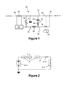
- a module 30 forming part of a circuit breaker apparatus 32 according to an embodiment of the invention is shown in Figure 1 .
- the circuit breaker apparatus 32 comprises a plurality of series-connected modules 30.
- Each module 30 includes: first and second conduction paths 34,36; and first and second terminals 38,40.
- Each conduction path extends between the first and second terminals 38,40.
- the first and second terminals 38,40 of each module 30 are connected in series with a DC network 42 and an AC circuit breaker 44.
- the DC network 42 includes a lumped line impedance 46, a DC voltage source 48 and a DC load 50, as shown in Figure 2 .
- the first conduction path 34 includes a first mechanical switching element 52 in the form of a first vacuum interrupter with retractably engaged contact elements (not shown) located inside a first vacuum enclosure 54a, while the second conduction path 36 includes a second mechanical switching element 56 in the form of a second vacuum interrupter with retractably engaged contact elements (not shown) located inside a second vacuum enclosure 54b, as shown in Figure 3a .
- each mechanical switching element 52,56 one of the contact elements is movable relative to the vacuum enclosure 54a,54b to define a moveable contact element, while the other of the contact elements is fixed relative to the vacuum enclosure 54a,54b to define a fixed contact element.
- the first mechanical switching element 52 is rated to be able to carry a load current I N flowing in the DC network 42 during normal power transmission.
- Each mechanical switching element 52,56 is preferably rated to have a voltage withstand capability of 10 kV/mm. Thus, each mechanical switching element 52,56 is able to withstand voltages that exceed 20 kV when the contact elements of each mechanical switching element 52,56 are separated by a gap in the range of 2 to 3 mm.
- Each module 30 further includes a magnetic latching actuator 58, as shown in Figure 3a , that controls the switching of the first and second mechanical switching elements 52,56 to define a bistable mechanism that is in either a first configuration or a second configuration.
- a magnetic latching actuator 58 controls the switching of the first and second mechanical switching elements 52,56 to define a bistable mechanism that is in either a first configuration or a second configuration.
- the first mechanical switching element 52 is closed whilst the second mechanical switching element 56 is open.
- the first mechanical switching element 52 is open whilst the second mechanical switching element 56 is closed.
- Each module 30 further includes first and second insulating push rods 60a,60b.
- the movable contact element of the first mechanical switching element 52 is supported by the first insulating push rod 60a, while the fixed contact element of the first mechanical switching element 52 is supported by a first bolt 62a and a first pre-compressed spring 64a.
- the movable contact element of the second mechanical switching element 56 is supported by the second insulating push rod 60b, while the fixed contact element of the second mechanical switching element 56 is supported by a second bolt 62b and a second pre-compressed spring 64b.
- the first and second mechanical switching elements 52,56, the magnetic latching actuator 58, the insulating push rods 60a,60b and the pre-compressed springs 64a,64b are housed within a rigid, insulated housing 66, as shown in Figure 3a .
- Each pre-compressed spring 64a,64b is arranged between the corresponding vacuum enclosure 54a,54b and a wall 68a,68b of the housing 66. This allows each pre-compressed spring 64a,64b to apply a force to push the fixed contact element towards the movable contact element.
- the applied force acting between the contact elements must be sufficiently high to achieve the required current rating of the corresponding mechanical switching element 52,56.
- Each bolt 62a,62b is partially housed within the housing 66 and partially extends through a wall 68a,68b of the housing 66 so that its head 70a,70b is located outside the housing 66. This allows each bolt 62,62b to limit the maximum movement range of the corresponding pre-compressed spring 64,64b when its head 70a,70b is restrained by the corresponding wall 68a,68b of the housing 66.
- the first and second insulating push rods 60a,60b are coupled to the magnetic latching actuator 58 such that, in use, the magnetic latching actuator 58 moves the first and second insulating push rods 60a,60b to simultaneously push one of the movable contact elements towards its corresponding fixed contact element and pull the other of the movable contact elements away from its corresponding fixed contact element.
- Figure 3b illustrates the operation of the actuator to switch the bistable mechanism from its first configuration to its second configuration.
- the magnetic latching actuator 58 moves the first insulating push rod 60a to trigger separation of the contact elements of the first mechanical switching element 52. This is followed by relaxation of the first pre-compressed spring 64a, which keeps the moveable contact in contact 71 a with the fixed contact element until the movement of the first pre-compressed spring 64a is restrained by the first bolt 62a. At this instant, subsequent movement of the first insulating push rod 60a results in separation 71 b of the contact elements of the first mechanical switching element 52. At the same time, the magnetic latching actuator 58 moves, the second insulating push rod 60b to reduce 71 c the gap between the contact elements of the second mechanical switching element 56.
- the movable element stops moving 71 d and the second pre-compressed spring 64b applies a force to keep the contact elements in contact.
- the magnetic latching actuator 58 and insulating push rods 60a,60b are arranged so that the contact elements of the first mechanical switching element 52 are separated 71 e before the contact elements of the second mechanical switching element 56 are closed 71 d.
- bistable mechanism as set out above applies mutatis mutandis to the switching of the bistable mechanism from its second configuration to its first configuration.
- the configuration of the bistable mechanism therefore allows the first and second mechanical switching elements 52,56 to define a break-before-make switching arrangement.
- the operation of the magnetic latching actuator 58 preferably uses permanent magnets to maintain the latching of the bistable mechanism in either the first or second configuration, so that power is only required to operate the magnetic latching actuator 58 in order to move the insulating push rods 60a,60b.
- the magnetic latching actuator 58 may be replaced by another type of actuator that is able to couple the first and second mechanical switching elements 52,56 to define a break-before-make switching arrangement.
- an actuator may be, for example, a hydraulic actuator using de-ionised water or compressed air.
- first and second mechanical switching elements 52,56 may be separately switched, instead of being switched using a single actuator, to define the break-before-make switching arrangement.
- the second conduction path 36 further includes a commutation circuit 72, which includes a primary energy storage device 74 in the form of a capacitor, and an inductor 76.
- the primary energy storage device 74 and the inductor 76 is connected in series with the second mechanical switching element 56.
- the series-connection of the primary energy storage device 74 and the inductor 76 means that, in other embodiments, they may be connected in reverse order within the second conduction path 36.
- the primary energy storage device 74 does not form part of the commutation circuit 72, and the commutation circuit 72 may further include an additional energy storage device that is distinct from the primary energy storage device 74.
- Each module 30 further includes a snubber circuit 78, which includes a secondary energy storage device 80 in the form of a capacitor that is connected in series with a resistor 82.
- the snubber circuit 78 bridges the first and second conduction paths 34,36 and is connected in parallel with the commutation circuit 72.
- the series-connection of the secondary energy storage device 80 and the resistor 82 means that, in other embodiments, they may be connected in reverse order within the snubber circuit 78.
- the snubber circuit 78 may be connected in parallel with the first mechanical switching element 52.
- Each module 30 further includes a non-linear surge arrestor 84 that is connected in parallel with the primary energy storage device 74.
- the purpose of the surge arrestor 84 is to divert charging current away from the primary energy storage device 74 in order to limit a maximum voltage across the primary energy storage device 74. This not only keeps voltage stresses appearing across the components of each module 30 to within safe levels, but also dampens any voltage over-swing that may result from the resonant nature of the commutation circuit 72.
- the surge arrestor may be replaced by or used in combination with a resistive element that includes at least one non-linear resistor and/or at least one linear resistor.
- each module may further include an auxiliary switching element connected to the resistive element, the auxiliary switching element being operable to modify flow of current through or voltage drop across the resistive element.
- the use of the auxiliary switching element allows the resistive element to be selectively switched into or out of circuit to modify the flow of current through or voltage drop across the resistive element so as to control absorption and dissipation of energy by the resistive element.
- Each module 30 further includes a charging circuit, which includes a shunt 86 and a converter 88.
- the shunt 86 is connected in series between the first and second terminals 38,40.
- the flow of current between the first and second terminals 38,40 introduces a voltage drop across the shunt 86, which allows part of the current to be diverted 90 to a converter 88.
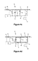
- the converter 88 harvests power from the diverted current 90 to charge 92 the primary energy storage device 74, as shown in Figure 4a .
- Each module 30 further includes local electronics (not shown) that are used to operate the magnetic latching actuator 58 and enable communication between each module 30 and ground control (not shown).
- the local electronics may be powered by:
- the magnetic latching actuator 58 switches the first and second mechanical switching elements 52,56 to the first configuration of the bistable mechanism, as shown in Figure 4b .
- This allows a load current I N to flow from the DC voltage source 48 to the DC load 50 through the first conduction path 34 of each module 30 and the series-connected AC circuit breaker 44.
- the load current I N does not flow through the second conduction path 36 of each module 30.
- the primary energy storage device 74 is charged to a predetermined voltage through use of the charging circuit, as shown in Figure 4a .
- a fault or other abnormal operating condition in the DC network 42 may lead to high fault current I F flowing through the DC network 42.
- the magnetic latching actuator 58 switches the first and second mechanical switching elements 52,56 to the second configuration of the bistable mechanism.
- the break-before-make switching arrangement of the first and second mechanical switching elements 52,56 results in the first mechanical switching element 52 being opened before the second mechanical switching element 56 is closed.
- the pre-charged primary energy storage device 74 begins to discharge.
- the resonance between the primary energy storage device 74 and the inductor 76 allows the commutation circuit 72 to establish a resonant current I R that flows in a circuit defined by the commutation circuit 72, the first mechanical switching element 52 and the second mechanical switching element 56, as shown in Figure 4d .
- the resonant current I R flows in the opposite direction to the arc current, and rises until it is equal in magnitude to the arc current. At this instant the resonant current I R and arc current cancel out, resulting in quenching of the arc current across the first mechanical switching element 52. This results in commutation of the fault current I F from the first conduction path 34 to the second conduction path 36, as shown in Figure 4e .
- the rate of change of current in the first mechanical switching element 52 is sufficiently slow, e.g. less than 100 A per ⁇ s, to allow condensation of metal ions present between the contact elements in order to minimise the amount of available metal ions and thereby reduce the risk of a re-strike of the arc across the contact elements.
- the snubber circuit 78 provides a current path for the residual current I L in the inductor 76, as shown in Figure 4e , to limit the rate of rise of voltage across the first mechanical switching element 52, preferably less than 20kV per ⁇ s, in order to preventing a re-strike of the arc across its contact elements.
- the snubber circuit 78 also provides a current path for any capacitive current flowing through the primary energy storage device 74 that arises from the primary energy storage device 74 experiencing a high rate of change of voltage when the resonant current I R and arc current cancel out, in order to preventing a re-strike of the arc across its contact elements.
- the inductor 76 of the commutation circuit 72 limits the peak value of the resonant current I R to minimise the stress on the components of the module 30.
- the flow of high fault current I F in the second conduction path 36 will result in rapid charging of the primary energy storage device 74, as shown in Figure 4f .
- This allows the primary energy storage device 74 of each module 30 to provide an opposing voltage to the voltage on the DC network 42.
- Each primary energy storage device 74 will continue to charge until the corresponding surge arrestor 84 conducts, or until the total opposing voltage provided by all the modules 30 is equal to the voltage on the DC network 42.
- each surge arrestor 84 conducts, it will absorb and dissipate inductive energy from the DC network 42.
- the total voltage capability of the surge arrestors 84 in the plurality of series-connected modules 30 must be greater than the normal operating voltage of the DC network 42, in order for the fault current I F to reduce to zero.
- the circuit breaker apparatus 32 may revert to its normal operating mode by operating the actuator to switch the first and second mechanical switching elements 52,56 to the first configuration of the bistable mechanism, so as to enable the DC network 42 to resume normal power transmission.
- some of the series-connected modules 30 are operated so that their first and second mechanical switching elements 52,56 are switched to define the second configuration of the bistable mechanism to allow their primary energy storage devices 74 to provide an opposing voltage, which opposes part of the current flowing through the DC network 42 and thereby drive the current to a lower non-zero value or prevent a further rise of current.
- the remaining modules 30 are operated so that their first and second mechanical switching elements 52,56 are switched to define the first configuration of the bistable mechanism, and so their primary energy storage devices 74 do not contribute any opposing voltage to drive the fault current I F to the lower non-zero value.
- the circuit breaker apparatus 32 is therefore capable of breaking and/or limiting current in the DC network 42.
- each module 30 provides a smooth commutation of current from the first conduction path 34 to the second conduction path 36.
- the use of mechanical switching elements 52,56 allows fast operation that is required for reliable current interruption but with a low actuation force, since each mechanical switching element 52,56 requires only a short travel distance of its contact elements to achieve a high voltage withstand.
- the first mechanical switching element 52 is able to quickly recover its full voltage blocking capability after the arc has been quenched, so as to reliably block current from flowing in the first conduction path 34 during the flow of fault current I F in the DC network 42.
- the configuration of each module 30 in the circuit breaker apparatus 32 therefore results in a reliable apparatus 32 that is able to rapidly respond to a fault occurring in the DC network 42.
- each module 30 results in a flexible circuit breaker apparatus 32 that is able to break or limit current in the DC network 42, irrespective of the direction of current flow between the circuit breaker apparatus 32 and the polarity of the voltage drop across the circuit breaker apparatus 32.
- Such a circuit breaker apparatus 32 is desirable for use with a DC network 42 in which the direction of load current I N typically bears no relation to the direction of fault current I F .
- a model of the operation of the circuit breaker apparatus 32 to carry out the current-breaking procedure illustrated in Figures 4a to 4f was simulated using MATLAB/Simulink, and the results of the simulation is shown in Figures 5a, 5b , 6a, 6b and 7 .
- the DC network 42 has a DC voltage of 500kV and a load current of 3.5kA
- the plurality of series-connected modules 30 was simulated as a combined module 30 having a single primary energy storage device 74 with a capacitance of 35 ⁇ F.
- the secondary energy storage device 80 of the snubber circuit 78 has a capacitance of 3.5 ⁇ F and the resistor 82 of the snubber circuit 78 has a resistance of 10 ⁇ .
- a trip current threshold for the circuit breaker apparatus 32 was arbitrarily set to 20kA for the purposes of the model.
- the value of the trip current threshold must be sufficiently high to provide enough time to detect a fast-rising fault current I F and operate the circuit breaker apparatus 32, and sufficiently low to prevent damage to the DC network 42 by the time the circuit breaker apparatus 32 has been operated.
- the occurrence of the fault results in a fault current I F that rises at a rate of nominally 6 kA per ms, which is limited by the impedance of the DC network 42. If the fault current I F is to be interrupted before it reaches 20kA and the primary energy storage device 74 of the combined module 30 is pre-charged to 200kV, the required inductor value to establish a resonant current that exceeds the arc current is given by Equation 1.
- C is the capacitance of the pre-charged primary energy storage device 74; V is the voltage across the pre-charged primary energy storage device 74; L is the inductance of the inductor 76; I F is the fault current to be interrupted.
- Equation 1 may be rewritten to take into account the rise in fault current I F .
- Equation 2 is used to determine the required value of the inductor 76 of the commutation circuit 72.
- Equation 1 the required value for the inductor 76 calculated using Equation 2 will be smaller than the value calculated using Equation 1.
- Figures 5a and 5b illustrate the changes in current 100,102 in the first and second conduction paths 34,36 in a simulated operation of the module 30 of Figure 1 to carry out the current-breaking procedure illustrated in Figures 4a to 4f .
- the occurrence of the fault in the DC network 42 gives rise to the fault current I F in the first conduction path 34 that rises at a rate of 6 kA per ms.
- the actuator 58 opens the first mechanical switching element 52. This results in an arc current across the contact elements of the first mechanical switching element 52 that maintains the flow of fault current I F in the first conduction path 34.
- the actuator 58 closes the second mechanical switching element 56 to allow the commutation circuit 72 to establish the resonant current I R that opposes the arc current and rises with time. Meanwhile the snubber circuit 78 causes a rapid change in current flowing through the first conduction path 34, which is depicted by a vertical edge 103 in Figure 5b .
- the resonant current I R When the resonant current I R is equal in magnitude to the arc current, the resonant current I R and the arc current cancel out, resulting in quenching of the arc current across the first mechanical switching element 52. At this stage the fault current I F is commutated from the first conduction path 34 to the second conduction path 36. Once the arc has been quenched, it takes time for the energy in the inductor 76 to settle, resulting in a delay before the peak fault current I F is reached at 44.5ms.
- the flow of fault current I F in the second conduction path 36 charges the primary energy storage device 74 of the combined module 30.
- the formation of the opposing voltage causes the fault current I F to cease flowing and thereby results in the collapse of the voltage 106 across the DC load to zero, as shown in Figure 7 .
- the operation of the circuit breaker apparatus 32 to carry out a current-breaking procedure therefore results in the primary energy storage devices 74 of the plurality of series-connected modules 30 being charged to provide an opposing voltage that cancels out the DC voltage on the DC network 42.
- the voltage across the primary energy storage device 74 after the current-breaking procedure is opposite in polarity to the voltage across the primary energy storage device 74 prior to the current-breaking procedure.
- circuit breaker apparatus 32 may be required to revert to its normal operating mode within a predetermined period of time after the initial current-breaking procedure.
- Switching the circuit breaker apparatus 32 to its normal operating mode results in current flow through the first conduction path 34.
- the absence of current in the second conduction path 36 before switching the first and second mechanical switching elements 52,56 to define the first configuration of the bistable mechanism means that an arc current does not form across the second mechanical switching element 56. Since the actuator controls the switching of the first and second mechanical switching elements 52,56 as a break-before-make switching arrangement, the lack of an arc current across the second mechanical switching element 56 means that there is no conduction overlap between the first and second mechanical switching elements 52,56. This prevents the commutation circuit 72 from establishing a resonant current that is able to charge the primary energy storage device 74, so that it reverts to its voltage prior to the first current-breaking procedure.
- a model of the operation of the circuit breaker apparatus 32 to carry out the initial and subsequent current-breaking procedure 114,116 was simulated using MATLAB/Simulink, and the results of the simulation is shown in Figures 9a , 9b and 10 .
- This model shares the same parameters as the earlier model with respect to the combined module 30 and the DC network 42.
- Figures 9a and 9b illustrate the changes in current 118,120 in the first and second conduction paths in a simulated operation of the module of Figure 1 to carry out a subsequent current-breaking procedure following completion of the current-breaking procedure illustrated in Figures 4a to 4f .
- the primary energy storage device 74 being charged to the opposite polarity prior to the subsequent current-breaking procedure 116 means that the time taken for the commutation of the fault current I F from the first conduction path 34 to the second conduction path 36 is more than 1.0 ms, i.e. approximately half of the resonant sinusoidal cycle.
- the voltage 122a across the primary energy storage device 74 prior to the subsequent current-breaking procedure 116 is at a comparable magnitude to the voltage rating of the DC voltage source 48, and is higher than the voltage 122b across the primary energy storage device 74 prior to the initial current-breaking procedure 114. This results in a higher peak resonant current 124 during the subsequent current-breaking procedure 116 than during the initial current-breaking procedure.
Abstract
the or each module (30) including: first and second conduction paths (34,36); and first and second terminals (38,40) for connection to an electrical network (42), each conduction path (34,36) extending between the first and second terminals (38,40);
the first conduction path (34) including a first mechanical switching element (52) to selectively close to allow current to flow between the first and second terminals (38,40) through the first conduction path (34) in a first mode of operation, or open to block current from flowing between the first and second terminals (38,40) through the first conduction path (34) in a second mode of operation;
the second conduction path (36) including a second mechanical switching element (56) to selectively open to block current from flowing between the first and second terminals (38,40) through the second conduction path (36) in the first mode of operation, or close to allow current to flow between the first and second terminals (38,40) through the second conduction path (36) in the second mode of operation, wherein the first and second mechanical switching elements (34,36) define a break-before-make switching arrangement;
the second conduction path (36) further including a primary energy storage device (74) to oppose current flowing between the first and second terminals (38,40) through the second conduction path (36) in the second mode of operation; and
the or each module (30) further including a commutation circuit (72) to establish a resonant current in the first mechanical switching element to quench an arc current appearing across the first mechanical switching element (52) in the second mode of operation.
Description
- This invention relates to a circuit breaker apparatus for use in high voltage direct current (HVDC) power transmission.
- In power transmission networks alternating current (AC) power is typically converted to direct current (DC) power for transmission via overhead lines and/or undersea cables. This conversion removes the need to compensate for the AC capacitive load effects imposed by the transmission line or cable, and thereby reduces the cost per kilometer of the lines and/or cables. Conversion from AC to DC thus becomes cost-effective when power needs to be transmitted over a long distance.
- The conversion of AC to DC power is also utilized in power transmission networks where it is necessary to interconnect AC networks operating at different frequencies. In any such power transmission network, converters are required at each interface between AC and DC power to effect the required conversion.
- HVDC converters are vulnerable to DC side faults or other abnormal operating conditions that can present a short circuit with low impedance across the DC power transmission lines or cables. Such faults can occur due to damage or breakdown of insulation, lightning strikes, movement of conductors or other accidental bridging between conductors by a foreign object.
- The presence of low impedance across the DC power transmission lines or cables can be detrimental to a HVDC converter. Sometimes the inherent design of the converter means that it cannot limit current under such conditions, resulting in the development of a high fault current exceeding the current rating of the HVDC converter. Such a high fault current not only damages components of the HVDC converter, but also results in the HVDC converter being offline for a period of time. This results in increased cost of repair and maintenance of damaged electrical apparatus hardware, and inconvenience to end users relying on the working of the electrical apparatus. It is therefore important to be able to interrupt the high fault current as soon as it is detected.
- A conventional means of protecting a HVDC converter from DC side faults, whereby the converter control cannot limit the fault current by any other means, is to trip an AC side circuit breaker, thus removing the supply of current that feeds the fault through the HVDC converter to the DC side. This is because there are currently no available HVDC circuit breaker designs. Furthermore, almost all HVDC schemes are currently point-to-point schemes with two HVDC converters connected to the DC side, whereby one HVDC converter acts as a power source with power rectification capability and the other HVDC converter acts as a power load with power inversion capability. Hence, tripping the AC side circuit breaker is acceptable because the presence of a fault in the point-to-point scheme requires interruption of power flow to allow the fault to be cleared.
- A new class of HVDC power transmission networks are being considered for moving large quantities of power over long distances, as required by geographically dispersed renewable forms of generation, and to augment existing capabilities of AC power transmission networks with smartgrid intelligence and features that are able to support modern electricity trading requirements.
- Such a HVDC power transmission network requires multi-terminal interconnection of HVDC converters, whereby power can be exchanged on the DC side using three or more HVDC converters operating in parallel. Each HVDC converter acts as either a source or sink to maintain the overall input-to-output power balance of the network whilst exchanging the power as required. Faults in the HVDC power transmission network need to be quickly isolated and segregated from the rest of the network in order to enable the network to resume normal power transmission as soon as possible.
- Current interruption in conventional circuit breakers is carried out when the current reaches a current zero, so as to considerably reduce the difficulty of the interruption task. Thus, in conventional circuit breakers, there is a risk of damage to the current interruption apparatus if a current zero does not occur within a defined time period for interrupting the current. It is therefore inherently difficult to carry out DC current interruption because, unlike AC current in which current zeros naturally occur, DC current cannot naturally reach a current zero.
-
EP 0 867 998 B1 - According to an aspect of the invention, there is provided a circuit breaker apparatus comprising a module, the module including first and second conduction paths and first and second terminals for connection to an electrical network, each conduction path extending between the first and second terminals;
the first conduction path including a first mechanical switching element to selectively close to allow current to flow between the first and second terminals through the first conduction path in a first mode of operation, or open to block current from flowing between the first and second terminals through the first conduction path in a second mode of operation;
the second conduction path including a second mechanical switching element to selectively open to block current from flowing between the first and second terminals through the second conduction path in the first mode of operation, or close to allow current to flow between the first and second terminals through the second conduction path in the second mode of operation, wherein the first and second mechanical switching elements define a break-before-make switching arrangement;
the second conduction path further including a primary energy storage device to oppose current flowing between the first and second terminals through the second conduction path in the second mode of operation; and
the module further including a commutation circuit to establish a resonant current in the first mechanical switching element to quench an arc current appearing across the first mechanical switching element in the second mode of operation. - In use, the circuit breaker apparatus may be connected in series with a DC network, and may be further connected in series with a conventional AC circuit breaker or disconnector. Connecting the circuit breaker apparatus to the DC network, closing the first mechanical switching element of the module and opening the second mechanical switching element of the module causes a load current to flow through the first conduction path of the module during normal power transmission in the DC network.
- In the event of a fault occurring in the DC network resulting in high fault current in the first conduction path of the module, the first mechanical switching element of the module is opened. This results in formation of an arc current between contact elements of the first mechanical switching element of the module. The second mechanical switching element of the module is then closed, and the commutation circuit of the module establishes a resonant current in the first mechanical switching element that opposes the arc current. The resonant current will rise until it is equal in magnitude to the arc current. At this instant the resonant and arc currents cancel out, resulting in quenching of the arc current across the first mechanical switching element of the module.
- Quenching the arc current across the first mechanical switching element of the module diverts the fault current into the second conduction path. This allows the primary energy storage device of the module to charge in order to provide an opposing voltage to the voltage on the DC network. The opposing voltage forms across the module or a plurality of series-connected modules when coordinated together, and is capable of driving the fault current to a defined value. The circuit breaker apparatus must be designed to contain enough modules connected in series to have a sufficient collective voltage margin to cope with the nominal voltage rating of the DC network in order to drive the fault current to zero. The inclusion of the primary energy storage device in the second conduction path of the module therefore allows the fault current to be suppressed in a controlled manner.
- If the current is driven to zero, the apparatus behaves as a circuit breaker. A second conventional AC circuit breaker or disconnector connected in series with the apparatus may then be switched to an open state to complete the circuit breaking process by providing isolation for safety purposes. Otherwise, if the opposing voltage drives the current to a non-zero value, then the apparatus behaves as a current limiter. In this case, the conventional AC circuit breaker may either remain closed or may be omitted in the first place.
- After the fault in the DC network has been cleared, the circuit breaker apparatus may revert to its normal operating mode by opening the second mechanical switching element and closing the first mechanical switching element, so as to enable the DC network to resume normal power transmission.
- The configuration of the module in the circuit breaker apparatus therefore results in the module forming a self-contained unit that can selectively apply a voltage drop into the DC network.
- In embodiments of the invention the circuit apparatus may comprise a plurality of such modules connected in series. In such embodiments the circuit breaker apparatus may be used to either break or limit current in a DC network. The number of modules provided can be varied to suit low-, medium- and high-voltage electrical applications but is usually rated such that use of all modules drives the current to zero in a given application. In addition, the use of a plurality of series-connected modules in the circuit breaker apparatus allows the overall DC network voltage rating to be sub-divided into individual voltage ratings for the plurality of series-connected modules, which may number in the hundreds. This allows the use of freely available medium-voltage mechanical switching elements, resulting in a practical and cost-efficient circuit breaker apparatus.
- The use of the mechanical switching elements and commutation circuit in the or each module provides a smooth commutation of current from the first conduction path to the second conduction path. In addition, the use of mechanical switching elements allows fast operation that is required for reliable current interruption but with a low actuation force, since each mechanical switching element requires only a short travel distance of its contact elements to achieve a high voltage withstand. Furthermore the first mechanical switching element is able to quickly recover its full voltage blocking capability after the arc has been quenched, so as to reliably block current from flowing in the first conduction path when operating in the second mode of operation. The configuration of the or each module in the circuit breaker apparatus therefore results in a reliable apparatus that is able to rapidly respond to a fault occurring in the DC network.
- Moreover the non-polarised configuration of the or each module results in a flexible circuit breaker apparatus that is able to break or limit current in the DC network, irrespective of the direction of current flow between the circuit breaker apparatus and the polarity of the voltage drop across the circuit breaker apparatus. Such a circuit breaker apparatus is desirable for use with a DC network in which the direction of load current typically bears no relation to the direction of fault current.
- In order to limit current in the DC network, the circuit breaker apparatus may be operated such that only some of the modules provide an opposing voltage to drive the current to a non-zero value, while the remaining modules do not provide an opposing voltage.
- The current-limiting operation may be achieved through use of an embodiment of the circuit breaker apparatus, in which the circuit breaker apparatus includes a plurality of series-connected modules, wherein the first and second mechanical switching elements of one or more modules when operating in the first mode of operation are switched to direct current flowing between the first and second terminals through the first conduction path and away from the second conduction path, whilst the first and second mechanical switching elements of the or each other module when operating in the second mode of operation are switched to direct current flowing between the first and second terminals through the second conduction path and away from the first conduction path. This allows the opposing voltage to be adjusted to drive the current to any non-zero value that is less than the original fault current level.
- The circuit breaker apparatus preferably further includes an actuator to switch the first and second mechanical switching elements. Such an actuator may be, for example, a magnetic latching actuator, or a hydraulic actuator using de-ionised water or compressed air.
- The use of a single actuator to control the switching of the first and second mechanical switching elements in the or each module simplifies the operation of the circuit breaker apparatus.
- In embodiments of the invention, the commutation circuit may include: an energy storage device to discharge to establish the resonant current in the second mode of operation; and an inductor.
- The energy storage device and inductor of the commutation circuit are rated such that the commutation circuit is able to establish a peak resonant current that exceeds the fault current passing through the circuit breaker apparatus.
- In embodiments employing the use of the commutation circuit, the second conduction path may include the commutation circuit, and the energy storage device and inductor of the commutation circuit may be connected in series with the second mechanical switching element. This allows the closing of the second mechanical switching element to trigger the operation of the commutation circuit to establish the resonant current, thus simplifying the operation of the or each module.
- In further embodiments employing the use of the commutation circuit, the primary energy storage device may define the energy storage device of the commutation circuit.
- Integrating the primary energy storage device into the commutation circuit advantageously minimises the number of components in the or each module, which in turn reduces the overall cost, size and weight of the circuit breaker apparatus.
- In such embodiments, the energy storage device of the commutation circuit may be charged, in use, to a predetermined voltage in the first mode of operation. This allows the energy storage device of the commutation circuit when operating in the second mode of operation to rapidly establish the required resonant current, so as to improve the response time of the circuit breaker apparatus to the occurrence of the fault in the DC network.
- In embodiments of the invention, the or each module may include a resistive element and/or a surge arrestor to divert charging current from the first and second terminals away from the primary energy storage device to limit a maximum voltage across the primary energy storage device. This is achieved by the resistive element and/or surge arrestor absorbing and dissipating inductive energy from the DC network when the voltage across the primary energy storage device reaches a particular voltage.
- The use of the resistive element and/or surge arrestor to divert the charging current away from the primary energy storage device not only keeps voltage stresses appearing across the components of the or each module to within safe levels, but also dampens any voltage over-swing that may result from the resonant nature of the commutation circuit.
- Preferably the surge arrestor is a non-linear surge arrestor.
- In embodiments employing the use of the resistive element, the resistive element may include at least one linear resistor and/or at least one non-linear resistor, e.g. a metal-oxide varistor.
- In further embodiments employing the use of the resistive element, the or each module may further include an auxiliary switching element connected to the resistive element, the auxiliary switching element being operable to modify flow of current through or voltage drop across the resistive element.
- The use of the auxiliary switching element allows the resistive element to be selectively switched into or out of circuit to modify the flow of current through or voltage drop across the resistive element so as to control absorption and dissipation of energy by the resistive element. When the resistive element consists of a plurality of resistive element parts, the auxiliary switching element and the plurality of resistive element parts may be arranged so that the auxiliary switching element is able to switch some of the resistive element parts, instead of the entire resistive element, out of circuit when modifying the flow of current through or the voltage drop across the resistive element, whilst the other resistive element parts remain in circuit.
- The resistive element is preferably connected in parallel with the primary energy storage device.
- In embodiments of the invention, the or each module may further include a snubber circuit to control a rate of change of voltage across the first mechanical switching element in the second mode of operation The snubber circuit may, for example, include a secondary energy storage device connected in series with a resistor.
- The commutation of fault current from the first conduction path to the second conduction path may give rise to a rapid change in voltage across the contact elements of the first mechanical switching element. The snubber circuit acts to limit the rate of rise of voltage across the first switching element to prevent an arc restriking across the contact elements of the first switching element.
- The snubber circuit may be arranged in the or each module to form different configurations in order to control a rate of change of voltage across the first mechanical switching element in the second mode of operation. In one such configuration, the snubber circuit may define a bridge between the first and second conduction paths, and may be connected in parallel with the commutation circuit. In another such configuration, the snubber circuit may be connected in parallel with the first mechanical switching element.
- Preferably each mechanical switching element includes retractably engaged contact elements located within a dielectric medium.
- The choice of dielectric medium affects the voltage withstand capability of each mechanical switching element. The dielectric medium may be a high-performance dielectric medium, which may be, but not limited to oil, vacuum or sulphur hexafluoride. Use of high-performance dielectric media enables a small separation between the contact elements of each mechanical switching element to result in a high isolation voltage. This in turn facilitates rapid switching of each mechanical switching element, since the contact elements are only required to travel a short distance to achieve the required separation. A short separation between the contact elements also reduces the actuation energy required to operate the mechanical switching element, thus reducing the overall size, cost and weight of the circuit breaker apparatus.
- In embodiments of the invention, the circuit breaker apparatus may further include a charging circuit, wherein the charging circuit includes a shunt and a converter, the shunt diverting part of the current flowing, in use, between the first and second terminals into the converter to harvest power from the diverted current so as to charge the primary energy storage device. This allows the energy storage device of the commutation circuit to the predetermined voltage in the first mode of operation.
- In further embodiments of the invention, the circuit breaker apparatus may include a plurality of series-connected modules, and, in use, the first and second mechanical switching elements of the plurality of series-connected modules may be sequentially switched to momentarily direct a current through the second conduction path of each module at different intervals for different modules.
- The switching of the first and second mechanical switching elements of the plurality of series-connected modules in this manner allows each primary energy storage device to charge at regular intervals. The voltage drop provided by each module during the sequential switching process is very small when compared to the overall DC voltage of the DC network. Power for local electronics associated with each module may then be sourced directly from the corresponding primary energy storage device.
- A preferred embodiment of the invention will now be described, by way of a non-limiting example, with reference to the accompanying drawings in which:
-
Figure 1 shows, in schematic form, a module forming part of a circuit breaker apparatus according to an embodiment of the invention; -
Figure 2 shows, in schematic form, the circuit breaker apparatus in connection with a DC network; -
Figure 3a shows a magnetic latching actuator that is operable to switch the first and second mechanical switching elements of the module ofFigure 1 ; -
Figure 3b illustrates the operation of the magnetic latching actuator ofFigure 3a to switch the first and second mechanical switching elements of the module ofFigure 1 ; -
Figures 4a to 4f illustrate the operation of the module ofFigure 1 to carry out a current-breaking procedure -
Figures 5a and 5b illustrate the changes in current in the first and second conduction paths in a simulated operation of the module ofFigure 1 to carry out the current-breaking procedure illustrated inFigures 4a to 4f ; -
Figures 6a and 6b illustrate the change in voltage across the primary energy storage device in a simulated operation of the module ofFigure 1 to carry out the current-breaking procedure illustrated inFigures 4a to 4f ; -
Figure 7 illustrate the change in voltage across a DC load in a simulated operation of the module ofFigure 1 to carry out the current-breaking procedure illustrated inFigures 4a to 4f ; -
Figure 8a illustrates the commutation of current from the first conduction path to the second conduction path in a simulated operation of the module ofFigure 1 to carry out the current-breaking procedure illustrated inFigures 4a to 4f ; -
Figure 8b illustrates the commutation of current from the first conduction path to the second conduction path in a simulated operation of the module ofFigure 1 to carry out a subsequent current-breaking procedure following completion of the current-breaking procedure illustrated inFigures 4a to 4f ; -
Figures 9a and9b illustrate the changes in current in the first and second conduction paths in a simulated operation of the module ofFigure 1 to carry out a subsequent current-breaking procedure following completion of the current-breaking procedure illustrated inFigures 4a to 4f ; and -
Figure 10 illustrates the change in voltage across the primary energy storage device in a simulated operation of the module ofFigure 1 to a subsequent current-breaking procedure following completion of the current-breaking procedure illustrated inFigures 4a to 4f . - A
module 30 forming part of acircuit breaker apparatus 32 according to an embodiment of the invention is shown inFigure 1 . - The
circuit breaker apparatus 32 comprises a plurality of series-connectedmodules 30. Eachmodule 30 includes: first andsecond conduction paths second terminals second terminals - In use, the first and
second terminals module 30 are connected in series with a DC network 42 and anAC circuit breaker 44. The DC network 42 includes a lumped line impedance 46, a DC voltage source 48 and aDC load 50, as shown inFigure 2 . - The
first conduction path 34 includes a firstmechanical switching element 52 in the form of a first vacuum interrupter with retractably engaged contact elements (not shown) located inside a first vacuum enclosure 54a, while thesecond conduction path 36 includes a second mechanical switchingelement 56 in the form of a second vacuum interrupter with retractably engaged contact elements (not shown) located inside asecond vacuum enclosure 54b, as shown inFigure 3a . - In each
mechanical switching element vacuum enclosure 54a,54b to define a moveable contact element, while the other of the contact elements is fixed relative to thevacuum enclosure 54a,54b to define a fixed contact element. - The first
mechanical switching element 52 is rated to be able to carry a load current IN flowing in the DC network 42 during normal power transmission. - Each
mechanical switching element mechanical switching element mechanical switching element - Each
module 30 further includes amagnetic latching actuator 58, as shown inFigure 3a , that controls the switching of the first and secondmechanical switching elements mechanical switching element 52 is closed whilst the second mechanical switchingelement 56 is open. In the second configuration, the firstmechanical switching element 52 is open whilst the second mechanical switchingelement 56 is closed. - Each
module 30 further includes first and second insulatingpush rods mechanical switching element 52 is supported by the first insulatingpush rod 60a, while the fixed contact element of the firstmechanical switching element 52 is supported by afirst bolt 62a and a firstpre-compressed spring 64a. Similarly, the movable contact element of the second mechanical switchingelement 56 is supported by the second insulatingpush rod 60b, while the fixed contact element of the second mechanical switchingelement 56 is supported by asecond bolt 62b and a secondpre-compressed spring 64b. - The first and second
mechanical switching elements magnetic latching actuator 58, the insulatingpush rods pre-compressed springs Figure 3a . Eachpre-compressed spring corresponding vacuum enclosure 54a,54b and awall pre-compressed spring mechanical switching element - Each
bolt wall head bolt 62,62b to limit the maximum movement range of the correspondingpre-compressed spring 64,64b when itshead corresponding wall - The first and second insulating
push rods magnetic latching actuator 58 such that, in use, themagnetic latching actuator 58 moves the first and second insulatingpush rods -
Figure 3b illustrates the operation of the actuator to switch the bistable mechanism from its first configuration to its second configuration. - To switch the bistable mechanism from its first configuration to its second configuration, the
magnetic latching actuator 58 moves the first insulatingpush rod 60a to trigger separation of the contact elements of the firstmechanical switching element 52. This is followed by relaxation of the firstpre-compressed spring 64a, which keeps the moveable contact incontact 71 a with the fixed contact element until the movement of the firstpre-compressed spring 64a is restrained by thefirst bolt 62a. At this instant, subsequent movement of the first insulatingpush rod 60a results inseparation 71 b of the contact elements of the firstmechanical switching element 52. At the same time, themagnetic latching actuator 58 moves, the second insulatingpush rod 60b to reduce 71 c the gap between the contact elements of the second mechanical switchingelement 56. When the contact elements of the second mechanical switchingelement 56 are closed, the movable element stops moving 71 d and the secondpre-compressed spring 64b applies a force to keep the contact elements in contact. Themagnetic latching actuator 58 and insulatingpush rods mechanical switching element 52 are separated 71 e before the contact elements of the second mechanical switchingelement 56 are closed 71 d. - The operation of the bistable mechanism as set out above applies mutatis mutandis to the switching of the bistable mechanism from its second configuration to its first configuration.
- The configuration of the bistable mechanism therefore allows the first and second
mechanical switching elements - The operation of the
magnetic latching actuator 58 preferably uses permanent magnets to maintain the latching of the bistable mechanism in either the first or second configuration, so that power is only required to operate themagnetic latching actuator 58 in order to move the insulatingpush rods - It is envisaged that, in other embodiments of the invention, the
magnetic latching actuator 58 may be replaced by another type of actuator that is able to couple the first and secondmechanical switching elements - It is further envisaged that, in other embodiments of the invention, the first and second
mechanical switching elements - The
second conduction path 36 further includes acommutation circuit 72, which includes a primaryenergy storage device 74 in the form of a capacitor, and aninductor 76. The primaryenergy storage device 74 and theinductor 76 is connected in series with the second mechanical switchingelement 56. - The series-connection of the primary
energy storage device 74 and theinductor 76 means that, in other embodiments, they may be connected in reverse order within thesecond conduction path 36. - It is envisaged that, in other embodiments of the invention, the primary
energy storage device 74 does not form part of thecommutation circuit 72, and thecommutation circuit 72 may further include an additional energy storage device that is distinct from the primaryenergy storage device 74. - Each
module 30 further includes asnubber circuit 78, which includes a secondaryenergy storage device 80 in the form of a capacitor that is connected in series with aresistor 82. Thesnubber circuit 78 bridges the first andsecond conduction paths commutation circuit 72. - The series-connection of the secondary
energy storage device 80 and theresistor 82 means that, in other embodiments, they may be connected in reverse order within thesnubber circuit 78. - It is envisaged that, in other embodiments of the invention, the
snubber circuit 78 may be connected in parallel with the firstmechanical switching element 52. - Each
module 30 further includes anon-linear surge arrestor 84 that is connected in parallel with the primaryenergy storage device 74. The purpose of thesurge arrestor 84 is to divert charging current away from the primaryenergy storage device 74 in order to limit a maximum voltage across the primaryenergy storage device 74. This not only keeps voltage stresses appearing across the components of eachmodule 30 to within safe levels, but also dampens any voltage over-swing that may result from the resonant nature of thecommutation circuit 72. - It is envisaged that, in other embodiments of the invention, the surge arrestor may be replaced by or used in combination with a resistive element that includes at least one non-linear resistor and/or at least one linear resistor.
- It is further envisaged that, in further embodiments employing the use of the resistive element, each module may further include an auxiliary switching element connected to the resistive element, the auxiliary switching element being operable to modify flow of current through or voltage drop across the resistive element. The use of the auxiliary switching element allows the resistive element to be selectively switched into or out of circuit to modify the flow of current through or voltage drop across the resistive element so as to control absorption and dissipation of energy by the resistive element.
- Each
module 30 further includes a charging circuit, which includes ashunt 86 and aconverter 88. Theshunt 86 is connected in series between the first andsecond terminals second terminals shunt 86, which allows part of the current to be diverted 90 to aconverter 88. In turn, theconverter 88 harvests power from the diverted current 90 to charge 92 the primaryenergy storage device 74, as shown inFigure 4a . - Each
module 30 further includes local electronics (not shown) that are used to operate themagnetic latching actuator 58 and enable communication between eachmodule 30 and ground control (not shown). - It is envisaged that, in embodiments of the invention, the local electronics may be powered by:
- harvesting power directly from the DC voltage source 48;
- sequentially switching the first and second
mechanical switching elements different modules 30 at different intervals to momentarily direct the load current IN through thesecond conduction path 36. This allows each primaryenergy storage device 74 to charge to the surge arrestor voltage at regular intervals. The voltage drop provided by eachmodule 30 during the sequential switching process is very small when compared to the overall DC voltage of the DC network 42. The power for the local electronics may then be sourced directly from each primaryenergy storage device 74; - using a local reservoir capacitor and an auxiliary power supply to trickle-charge the reservoir capacitor to the required level over a period of, for example, 100ms. Since the delay between consecutive current-breaking procedures may be in the order of 3 ms, the pre-charged reservoir capacitor may not be charged to the required level after the first current-breaking procedure is completed. Two pre-charged reservoir capacitors may therefore be used to provide power to the local electronics for each current-breaking procedure. Rapid operation of the
magnetic latching actuator 58 may be achieved by operating theactuator 58 at high voltage and configuring the actuator coil to have a minimum number of turns. To convert the energy from the reservoir capacitor into current to operate theactuator 58, the reservoir capacitor may have a capacitance value that resonates with the actuator coil inductance, and a diode may be used to prevent the voltage of the reservoir capacitor going through zero in order to provide a sustained current for driving theactuator 58; or - an optically driven power supply.
- It will be appreciated that the use of a ground-based power supply to power the local electronics may be precluded if the operating voltage of the circuit breaker apparatus is too high for the ground-based power supply.
- Operation of each
module 30 of thecircuit breaker apparatus 32 inFigure 1 to break current in the DC network 42 is described as follows, with reference toFigures 4a to 4f . - During normal power transmission in the DC network 42, the
magnetic latching actuator 58 switches the first and secondmechanical switching elements Figure 4b . This allows a load current IN to flow from the DC voltage source 48 to theDC load 50 through thefirst conduction path 34 of eachmodule 30 and the series-connectedAC circuit breaker 44. At this stage the load current IN does not flow through thesecond conduction path 36 of eachmodule 30. Meanwhile the primaryenergy storage device 74 is charged to a predetermined voltage through use of the charging circuit, as shown inFigure 4a . - A fault or other abnormal operating condition in the DC network 42 may lead to high fault current IF flowing through the DC network 42.
- In response to an event of high fault current in the DC network 42, the
magnetic latching actuator 58 switches the first and secondmechanical switching elements - When the first
mechanical switching element 52 is opened, an arc current forms between the contact elements of the firstmechanical switching element 52. At this stage the fault current IF continues to flow in thefirst conduction path 34 due to the presence of the arc current, as shown inFigure 4c . - As mentioned above, the break-before-make switching arrangement of the first and second
mechanical switching elements mechanical switching element 52 being opened before the second mechanical switchingelement 56 is closed. - When the second mechanical switching
element 56 is closed, the pre-charged primaryenergy storage device 74 begins to discharge. The resonance between the primaryenergy storage device 74 and theinductor 76 allows thecommutation circuit 72 to establish a resonant current IR that flows in a circuit defined by thecommutation circuit 72, the firstmechanical switching element 52 and the second mechanical switchingelement 56, as shown inFigure 4d . The resonant current IR flows in the opposite direction to the arc current, and rises until it is equal in magnitude to the arc current. At this instant the resonant current IR and arc current cancel out, resulting in quenching of the arc current across the firstmechanical switching element 52. This results in commutation of the fault current IF from thefirst conduction path 34 to thesecond conduction path 36, as shown inFigure 4e . - Preferably, when the resonant current IR and arc current cancel out, the rate of change of current in the first
mechanical switching element 52 is sufficiently slow, e.g. less than 100 A per µs, to allow condensation of metal ions present between the contact elements in order to minimise the amount of available metal ions and thereby reduce the risk of a re-strike of the arc across the contact elements. - When the resonant current IR and arc current cancel out, a voltage appears across the
inductor 76. This results in the flow of residual current IL in theinductor 76. Thesnubber circuit 78 provides a current path for the residual current IL in theinductor 76, as shown inFigure 4e , to limit the rate of rise of voltage across the firstmechanical switching element 52, preferably less than 20kV per µs, in order to preventing a re-strike of the arc across its contact elements. - The
snubber circuit 78 also provides a current path for any capacitive current flowing through the primaryenergy storage device 74 that arises from the primaryenergy storage device 74 experiencing a high rate of change of voltage when the resonant current IR and arc current cancel out, in order to preventing a re-strike of the arc across its contact elements. - Meanwhile the
inductor 76 of thecommutation circuit 72 limits the peak value of the resonant current IR to minimise the stress on the components of themodule 30. - The flow of high fault current IF in the
second conduction path 36 will result in rapid charging of the primaryenergy storage device 74, as shown inFigure 4f . This allows the primaryenergy storage device 74 of eachmodule 30 to provide an opposing voltage to the voltage on the DC network 42. Each primaryenergy storage device 74 will continue to charge until thecorresponding surge arrestor 84 conducts, or until the total opposing voltage provided by all themodules 30 is equal to the voltage on the DC network 42. When eachsurge arrestor 84 conducts, it will absorb and dissipate inductive energy from the DC network 42. - If the DC network 42 is connected to a highly inductive network, the total voltage capability of the
surge arrestors 84 in the plurality of series-connectedmodules 30 must be greater than the normal operating voltage of the DC network 42, in order for the fault current IF to reduce to zero. - When the sum of the opposing voltages provided by the plurality of series-connected
modules 30 is equal to the voltage of the DC voltage source 48, the fault current IF will cease to flow in the DC network 42. This allows the series-connectedAC circuit breaker 44 to be opened to complete the current breaking procedure, thus allowing the fault in the DC network 42 to be cleared. - After the fault in the DC network 42 has been cleared, the
circuit breaker apparatus 32 may revert to its normal operating mode by operating the actuator to switch the first and secondmechanical switching elements - To operate the
circuit breaker apparatus 32 in a current-limiting mode, some of the series-connectedmodules 30 are operated so that their first and secondmechanical switching elements energy storage devices 74 to provide an opposing voltage, which opposes part of the current flowing through the DC network 42 and thereby drive the current to a lower non-zero value or prevent a further rise of current. Meanwhile the remainingmodules 30 are operated so that their first and secondmechanical switching elements energy storage devices 74 do not contribute any opposing voltage to drive the fault current IF to the lower non-zero value. - The
circuit breaker apparatus 32 is therefore capable of breaking and/or limiting current in the DC network 42. - The use of the
mechanical switching elements commutation circuit 72 in eachmodule 30 provides a smooth commutation of current from thefirst conduction path 34 to thesecond conduction path 36. In addition, the use ofmechanical switching elements mechanical switching element mechanical switching element 52 is able to quickly recover its full voltage blocking capability after the arc has been quenched, so as to reliably block current from flowing in thefirst conduction path 34 during the flow of fault current IF in the DC network 42. The configuration of eachmodule 30 in thecircuit breaker apparatus 32 therefore results in areliable apparatus 32 that is able to rapidly respond to a fault occurring in the DC network 42. - It will be appreciated that the non-polarised configuration of each
module 30 results in a flexiblecircuit breaker apparatus 32 that is able to break or limit current in the DC network 42, irrespective of the direction of current flow between thecircuit breaker apparatus 32 and the polarity of the voltage drop across thecircuit breaker apparatus 32. Such acircuit breaker apparatus 32 is desirable for use with a DC network 42 in which the direction of load current IN typically bears no relation to the direction of fault current IF. - A model of the operation of the
circuit breaker apparatus 32 to carry out the current-breaking procedure illustrated inFigures 4a to 4f was simulated using MATLAB/Simulink, and the results of the simulation is shown inFigures 5a, 5b ,6a, 6b and7 . - In the model, the DC network 42 has a DC voltage of 500kV and a load current of 3.5kA, and the plurality of series-connected
modules 30 was simulated as a combinedmodule 30 having a single primaryenergy storage device 74 with a capacitance of 35µF. In addition, in the combinedmodule 30, the secondaryenergy storage device 80 of thesnubber circuit 78 has a capacitance of 3.5µF and theresistor 82 of thesnubber circuit 78 has a resistance of 10Ω. - A trip current threshold for the
circuit breaker apparatus 32 was arbitrarily set to 20kA for the purposes of the model. The value of the trip current threshold must be sufficiently high to provide enough time to detect a fast-rising fault current IF and operate thecircuit breaker apparatus 32, and sufficiently low to prevent damage to the DC network 42 by the time thecircuit breaker apparatus 32 has been operated. - In the mode, a fault was set to occur on the DC network 42 at t = 40 ms. The occurrence of the fault results in a fault current IF that rises at a rate of nominally 6 kA per ms, which is limited by the impedance of the DC network 42. If the fault current IF is to be interrupted before it reaches 20kA and the primary
energy storage device 74 of the combinedmodule 30 is pre-charged to 200kV, the required inductor value to establish a resonant current that exceeds the arc current is given byEquation 1.
Where C is the capacitance of the pre-charged primaryenergy storage device 74;
V is the voltage across the pre-charged primaryenergy storage device 74;
L is the inductance of theinductor 76;
IF is the fault current to be interrupted. - If the operation of the
circuit breaker apparatus 32 is triggered by the fault current IF crossing the trip current threshold of 20 kA, the fault current IF can rapidly rise in the time taken to commutate the fault current from thefirst conduction path 34 to thesecond conduction path 36. Thus,Equation 1 may be rewritten to take into account the rise in fault current IF. This results inEquation 2 as follows, which is used to determine the required value of theinductor 76 of thecommutation circuit 72.
Where dl/dt is the rate of rise of fault current;
Δ T is the time taken to commutate the fault current IF from thefirst conduction path 34 to thesecond conduction path 36. - It can be seen from
Equations inductor 76 calculated usingEquation 2 will be smaller than the value calculated usingEquation 1. -
Figures 5a and 5b illustrate the changes in current 100,102 in the first andsecond conduction paths module 30 ofFigure 1 to carry out the current-breaking procedure illustrated inFigures 4a to 4f . - At t = 40 ms, the occurrence of the fault in the DC network 42 gives rise to the fault current IF in the
first conduction path 34 that rises at a rate of 6 kA per ms. During the rise in fault current IF, theactuator 58 opens the firstmechanical switching element 52. This results in an arc current across the contact elements of the firstmechanical switching element 52 that maintains the flow of fault current IF in thefirst conduction path 34. - At t = 43 ms, the
actuator 58 closes the second mechanical switchingelement 56 to allow thecommutation circuit 72 to establish the resonant current IR that opposes the arc current and rises with time. Meanwhile thesnubber circuit 78 causes a rapid change in current flowing through thefirst conduction path 34, which is depicted by avertical edge 103 inFigure 5b . - When the resonant current IR is equal in magnitude to the arc current, the resonant current IR and the arc current cancel out, resulting in quenching of the arc current across the first
mechanical switching element 52. At this stage the fault current IF is commutated from thefirst conduction path 34 to thesecond conduction path 36. Once the arc has been quenched, it takes time for the energy in theinductor 76 to settle, resulting in a delay before the peak fault current IF is reached at 44.5ms. - The flow of fault current IF in the
second conduction path 36 charges the primaryenergy storage device 74 of the combinedmodule 30. Thevoltage 104 across the primaryenergy storage device 74 starts to stabilise at t = 44.5 ms and eventually forms a steady-state opposing voltage of 500 kV, as shown inFigures 6a and 6b . The formation of the opposing voltage causes the fault current IF to cease flowing and thereby results in the collapse of the voltage 106 across the DC load to zero, as shown inFigure 7 . - The operation of the
circuit breaker apparatus 32 to carry out a current-breaking procedure therefore results in the primaryenergy storage devices 74 of the plurality of series-connectedmodules 30 being charged to provide an opposing voltage that cancels out the DC voltage on the DC network 42. The voltage across the primaryenergy storage device 74 after the current-breaking procedure is opposite in polarity to the voltage across the primaryenergy storage device 74 prior to the current-breaking procedure. - In practice, the
circuit breaker apparatus 32 may be required to revert to its normal operating mode within a predetermined period of time after the initial current-breaking procedure. - Switching the
circuit breaker apparatus 32 to its normal operating mode results in current flow through thefirst conduction path 34. The absence of current in thesecond conduction path 36 before switching the first and secondmechanical switching elements element 56. Since the actuator controls the switching of the first and secondmechanical switching elements element 56 means that there is no conduction overlap between the first and secondmechanical switching elements commutation circuit 72 from establishing a resonant current that is able to charge the primaryenergy storage device 74, so that it reverts to its voltage prior to the first current-breaking procedure. - If the fault on the DC network 42 is still present when the
circuit breaker apparatus 32 is switched to its normal operating mode, the resultant rise in fault current IF requires thecircuit breaker apparatus 32 to carry out a subsequent current-breaking procedure. - In the initial current-breaking procedure, since the primary
energy storage device 74 is charged to a voltage VC1 with the polarity needed to establish the required resonant current, it only takes approximately a quarter of a resonantsinusoidal cycle 108 for the resonant current IR to reach thelevel 110 required to cancel out the arc current across the firstmechanical switching element 52, as shown inFigure 8a . - In the subsequent current-breaking procedure, since the primary
energy storage device 74 is now charged to a voltage VC2 with a different polarity to its voltage prior to the initial current-breaking procedure, it takes approximately half to three-quarters of a resonant sinusoidalcurrent cycle 112 for the resonant current IR to reach thelevel 110 required to cancel out the arc current across the firstmechanical switching element 52, as shown inFigures 8a and8b . This is because, to carry out the subsequent current carrying procedure, it takes time to charge the primaryenergy storage device 74 to the polarity needed to establish the required resonant current IR. The delay in commutation may result in the fault current IF rising to a point where it exceeds the peak value of the resonant current IR. Thus, when determining the required inductorvalue using Equation 2, it is necessary to take into account the delay in commutation and the resulting rise in fault current IF. - A model of the operation of the
circuit breaker apparatus 32 to carry out the initial and subsequent current-breaking procedure 114,116 was simulated using MATLAB/Simulink, and the results of the simulation is shown inFigures 9a ,9b and 10 . This model shares the same parameters as the earlier model with respect to the combinedmodule 30 and the DC network 42. -
Figures 9a and9b illustrate the changes in current 118,120 in the first and second conduction paths in a simulated operation of the module ofFigure 1 to carry out a subsequent current-breaking procedure following completion of the current-breaking procedure illustrated inFigures 4a to 4f . - The fault occurs at t = 40 ms, and the
circuit breaker apparatus 32 is operated to carry out the initial current-breakingprocedure 114. Thecircuit breaker apparatus 32 reverts to its normal operating mode at t = 140 ms, but the presence of the fault requires the subsequent current-breakingprocedure 116 to be carried out. An initial current impulse is observed at t = 140.5 ms due to the presence of thesnubber circuit 78 in the combinedmodule 30. - As mentioned above, the primary
energy storage device 74 being charged to the opposite polarity prior to the subsequent current-breakingprocedure 116 means that the time taken for the commutation of the fault current IF from thefirst conduction path 34 to thesecond conduction path 36 is more than 1.0 ms, i.e. approximately half of the resonant sinusoidal cycle. - In
Figure 10 , thevoltage 122a across the primaryenergy storage device 74 prior to the subsequent current-breakingprocedure 116 is at a comparable magnitude to the voltage rating of the DC voltage source 48, and is higher than thevoltage 122b across the primaryenergy storage device 74 prior to the initial current-breakingprocedure 114. This results in a higher peak resonant current 124 during the subsequent current-breakingprocedure 116 than during the initial current-breaking procedure.
Claims (17)
- A circuit breaker apparatus comprising a module,
the module including: first and second conduction paths; and first and second terminals for connection to an electrical network, each conduction path extending between the first and second terminals;
the first conduction path including a first mechanical switching element to selectively close to allow current to flow between the first and second terminals through the first conduction path in a first mode of operation, or open to block current from flowing between the first and second terminals through the first conduction path in a second mode of operation;
the second conduction path including a second mechanical switching element to selectively open to block current from flowing between the first and second terminals through the second conduction path in the first mode of operation, or close to allow current to flow between the first and second terminals through the second conduction path in the second mode of operation, wherein the first and second mechanical switching elements define a break-before-make switching arrangement;
the second conduction path further including a primary energy storage device to oppose current flowing between the first and second terminals through the second conduction path in the second mode of operation; and
the module further including a commutation circuit to establish a resonant current in the first mechanical switching element to quench an arc current appearing across the first mechanical switching element in the second mode of operation. - A circuit breaker apparatus according to Claim 1 including a plurality of series-connected modules, wherein the first and second mechanical switching elements of one or more modules when operating in the first mode of operation are switched to direct current flowing between the first and second terminals through the first conduction path and away from the second conduction path, whilst the first and second mechanical switching elements of the or each other module when operating in the second mode of operation are switched to direct current flowing between the first and second terminals through the second conduction path and away from the first conduction path.
- A circuit breaker apparatus according to any preceding claim further including an actuator to switch the first and second mechanical switching elements.
- A circuit breaker apparatus according to any preceding claim wherein the commutation circuit includes: an energy storage device to discharge to establish the resonant current in the second mode of operation; and an inductor.
- A circuit breaker apparatus according to Claim 4 wherein the second conduction path includes the commutation circuit, and the energy storage device and inductor of the commutation circuit are connected in series with the second mechanical switching element.
- A circuit breaker apparatus according to Claim 4 or Claim 5 wherein the primary energy storage device defines the energy storage device of the commutation circuit.
- A circuit breaker apparatus according to any of Claims 4 to 6 wherein the energy storage device of the commutation circuit is charged, in use, to a predetermined voltage in the first mode of operation.
- A circuit breaker apparatus according to any preceding claim wherein the or each module includes a resistive element and/or a surge arrestor to divert charging current from the first and second terminals away from the primary energy storage device to limit a maximum voltage across the primary energy storage device.
- A circuit breaker apparatus according to Claim 8 wherein the resistive element includes at least one linear resistor and/or at least one non-linear resistor.
- A circuit breaker apparatus according to Claim 8 or Claim 9 wherein the or each module further includes an auxiliary switching element connected to the resistive element, the auxiliary switching element being operable to modify flow of current through or voltage drop across the resistive element.
- A circuit breaker apparatus according to any of Claims 8 to 10 wherein the resistive element is connected in parallel with the primary energy storage device.
- A circuit breaker apparatus according to any preceding claim wherein the or each module further includes a snubber circuit to control a rate of change of voltage across the first mechanical switching element in the second mode of operation.
- A circuit breaker apparatus according to Claim 12 wherein the snubber circuit defines a bridge between the first and second conduction paths, and is connected in parallel with the commutation circuit.
- A circuit breaker apparatus according to Claim 12 wherein the snubber circuit is connected in parallel with the first mechanical switching element.
- A circuit breaker apparatus according to any preceding claim wherein each mechanical switching element includes retractably engaged contact elements located within a dielectric medium.
- A circuit breaker apparatus according to any preceding claim further includes a charging circuit, wherein the charging circuit includes a shunt and a converter, the shunt diverting part of the current flowing, in use, between the first and second terminals into the converter to harvest power from the diverted current so as to charge the primary energy storage device.
- A circuit breaker apparatus according to any preceding claim including a plurality of series-connected modules, wherein, in use, the first and second mechanical switching elements of the plurality of series-connected modules are sequentially switched to momentarily direct a current through the second conduction path of each module at different intervals for different modules.
Priority Applications (3)
| Application Number | Priority Date | Filing Date | Title |
|---|---|---|---|
| EP20120275081 EP2669921A1 (en) | 2012-05-31 | 2012-05-31 | Circuit breaker apparatus |
| US14/404,286 US20150108090A1 (en) | 2012-05-31 | 2013-05-29 | Circuit breaker apparatus |
| PCT/EP2013/061097 WO2013178696A1 (en) | 2012-05-31 | 2013-05-29 | Circuit breaker apparatus |
Applications Claiming Priority (1)
| Application Number | Priority Date | Filing Date | Title |
|---|---|---|---|
| EP20120275081 EP2669921A1 (en) | 2012-05-31 | 2012-05-31 | Circuit breaker apparatus |
Publications (1)
| Publication Number | Publication Date |
|---|---|
| EP2669921A1 true EP2669921A1 (en) | 2013-12-04 |
Family
ID=48576400
Family Applications (1)
| Application Number | Title | Priority Date | Filing Date |
|---|---|---|---|
| EP20120275081 Withdrawn EP2669921A1 (en) | 2012-05-31 | 2012-05-31 | Circuit breaker apparatus |
Country Status (3)
| Country | Link |
|---|---|
| US (1) | US20150108090A1 (en) |
| EP (1) | EP2669921A1 (en) |
| WO (1) | WO2013178696A1 (en) |
Cited By (8)
| Publication number | Priority date | Publication date | Assignee | Title |
|---|---|---|---|---|
| CN104600693A (en) * | 2015-01-07 | 2015-05-06 | 中国科学院电工研究所 | Energy storage breaker for direct current power grid |
| US20160181866A1 (en) * | 2013-08-14 | 2016-06-23 | Cockerill Maintenance & Ingenierie S.A. | Remote protection and switching device for electrical systems |
| CN106159880A (en) * | 2015-03-27 | 2016-11-23 | 积能环保电机工程科技有限公司 | DC solid circuit breaker and distribution system |
| US9692226B2 (en) | 2012-08-23 | 2017-06-27 | General Electric Technology Gmbh | Circuit interruption device |
| US9791876B2 (en) | 2013-04-12 | 2017-10-17 | General Electric Technology Gmbh | Current limiter |
| US9972997B2 (en) | 2012-08-23 | 2018-05-15 | General Electric Technology Gmbh | Circuit interruption device |
| US10310003B2 (en) | 2014-02-19 | 2019-06-04 | General Electric Technology Gmbh | Fault location in DC networks |
| EP4080725A1 (en) * | 2021-04-23 | 2022-10-26 | ABB S.p.A. | Method for estimating the operating conditions of a switching apparatus |
Families Citing this family (4)
| Publication number | Priority date | Publication date | Assignee | Title |
|---|---|---|---|---|
| WO2014000790A1 (en) * | 2012-06-27 | 2014-01-03 | Abb Technology Ltd | A high voltage current interrupted and an actuator system for a high voltage current interruptor |
| KR101625481B1 (en) * | 2014-05-13 | 2016-05-31 | 엘에스산전 주식회사 | Fast Switch |
| DE102014214956A1 (en) * | 2014-07-30 | 2016-02-04 | Siemens Aktiengesellschaft | Current zero pulse with constant current gradient for interrupting a direct current |
| US10658830B2 (en) * | 2015-06-23 | 2020-05-19 | Nanyang Technological University | Power system and method of forming the same |
Citations (5)
| Publication number | Priority date | Publication date | Assignee | Title |
|---|---|---|---|---|
| US2849659A (en) * | 1953-03-25 | 1958-08-26 | Siemens Ag | Direct-current and alternatingcurrent circuit interrupters |
| FR1436174A (en) * | 1964-04-07 | 1966-04-22 | Thomson Houston Comp Francaise | High voltage direct current circuit breaking device |
| FR2013736A1 (en) * | 1968-07-05 | 1970-04-10 | Gen Electric | |
| DE4304863A1 (en) * | 1992-02-21 | 1993-08-26 | Hitachi Ltd | Commutating constant voltage circuit breaker - blocks flow of commutator current from commutator circuit to load in unloaded open operating condition |
| EP0867998A1 (en) * | 1997-03-24 | 1998-09-30 | Asea Brown Boveri Ab | A plant for transmitting electric power |
Family Cites Families (1)
| Publication number | Priority date | Publication date | Assignee | Title |
|---|---|---|---|---|
| US3597556A (en) * | 1970-01-16 | 1971-08-03 | Gen Electric | Vacuum-type circuit breaker with force-supplementing means for increasing current-carrying abilities |
-
2012
- 2012-05-31 EP EP20120275081 patent/EP2669921A1/en not_active Withdrawn
-
2013
- 2013-05-29 WO PCT/EP2013/061097 patent/WO2013178696A1/en active Application Filing
- 2013-05-29 US US14/404,286 patent/US20150108090A1/en not_active Abandoned
Patent Citations (6)
| Publication number | Priority date | Publication date | Assignee | Title |
|---|---|---|---|---|
| US2849659A (en) * | 1953-03-25 | 1958-08-26 | Siemens Ag | Direct-current and alternatingcurrent circuit interrupters |
| FR1436174A (en) * | 1964-04-07 | 1966-04-22 | Thomson Houston Comp Francaise | High voltage direct current circuit breaking device |
| FR2013736A1 (en) * | 1968-07-05 | 1970-04-10 | Gen Electric | |
| DE4304863A1 (en) * | 1992-02-21 | 1993-08-26 | Hitachi Ltd | Commutating constant voltage circuit breaker - blocks flow of commutator current from commutator circuit to load in unloaded open operating condition |
| EP0867998A1 (en) * | 1997-03-24 | 1998-09-30 | Asea Brown Boveri Ab | A plant for transmitting electric power |
| EP0867998B1 (en) | 1997-03-24 | 2007-03-28 | Abb Ab | A plant for transmitting electric power |
Non-Patent Citations (2)
| Title |
|---|
| BACHMANN B ET AL: "Development of a 500 kV air blast HVDC circuit breaker", IEEE TRANSACTIONS ON POWER APPARATUS AND SYSTEMS, IEEE INC. NEW YORK, US, vol. 9, no. PAS-104, 1 September 1985 (1985-09-01), pages 2460 - 2466, XP002076109, ISSN: 0018-9510 * |
| GREENWOOD A N ET AL: "THEORY AND APPLICATION OF THE COMMUTATION PRINCIPLE FOR HVDC CIRCUIT BREAKERS", IEEE TRANSACTIONS ON POWER APPARATUS AND SYSTEMS, IEEE INC. NEW YORK, US, vol. PAS91, no. 4, 1 July 1972 (1972-07-01), pages 1570 - 1574, XP002049258, ISSN: 0018-9510 * |
Cited By (12)
| Publication number | Priority date | Publication date | Assignee | Title |
|---|---|---|---|---|
| US9692226B2 (en) | 2012-08-23 | 2017-06-27 | General Electric Technology Gmbh | Circuit interruption device |
| US9972997B2 (en) | 2012-08-23 | 2018-05-15 | General Electric Technology Gmbh | Circuit interruption device |
| US9791876B2 (en) | 2013-04-12 | 2017-10-17 | General Electric Technology Gmbh | Current limiter |
| US20160181866A1 (en) * | 2013-08-14 | 2016-06-23 | Cockerill Maintenance & Ingenierie S.A. | Remote protection and switching device for electrical systems |
| US9793757B2 (en) * | 2013-08-14 | 2017-10-17 | Cmi Defence S.A. | Remote protection and switching device for electrical systems |
| US10310003B2 (en) | 2014-02-19 | 2019-06-04 | General Electric Technology Gmbh | Fault location in DC networks |
| CN104600693A (en) * | 2015-01-07 | 2015-05-06 | 中国科学院电工研究所 | Energy storage breaker for direct current power grid |
| CN104600693B (en) * | 2015-01-07 | 2017-01-18 | 中国科学院电工研究所 | Energy storage breaker for direct current power grid |
| CN106159880A (en) * | 2015-03-27 | 2016-11-23 | 积能环保电机工程科技有限公司 | DC solid circuit breaker and distribution system |
| CN107534438A (en) * | 2015-03-27 | 2018-01-02 | 积能环保电机工程科技有限公司 | DC solid circuit breaker and distribution system |
| CN106159880B (en) * | 2015-03-27 | 2019-07-12 | 积能环保电机工程科技有限公司 | DC solid circuit breaker and distribution system |
| EP4080725A1 (en) * | 2021-04-23 | 2022-10-26 | ABB S.p.A. | Method for estimating the operating conditions of a switching apparatus |
Also Published As
| Publication number | Publication date |
|---|---|
| US20150108090A1 (en) | 2015-04-23 |
| WO2013178696A1 (en) | 2013-12-05 |
Similar Documents
| Publication | Publication Date | Title |
|---|---|---|
| EP2669921A1 (en) | Circuit breaker apparatus | |
| EP2639805B1 (en) | Method, circuit breaker and switching unit for switching off high-voltage DC currents | |
| EP2777059B1 (en) | Hybrid dc circuit breaking device | |
| US9184003B2 (en) | Circuit breakers | |
| KR101183508B1 (en) | A dc current breaker | |
| US9478974B2 (en) | DC voltage circuit breaker | |
| US20150131189A1 (en) | Composite high voltage dc circuit breaker | |
| EP2701254B1 (en) | Circuit interruption device | |
| US20150116881A1 (en) | High voltage dc circuit breaker apparatus | |
| US9691560B2 (en) | Single- or multi-pole switching device, in particular for DC applications | |
| US5473494A (en) | Electrical power supply system | |
| EP2768102B1 (en) | Circuit interruption device | |
| KR101630093B1 (en) | High-voltage DC circuit breaker | |
| WO2015185096A1 (en) | High voltage dc circuit breaker unit | |
| CN101393818A (en) | High-voltage vacuum circuit breaker | |
| RU2458425C2 (en) | High-voltage switch with disconnector function and method of switch control | |
| KR20210104885A (en) | Current breaker device and control method for high voltage direct current with capacitive buffer circuit | |
| EP3286772B1 (en) | Bypass switch comprising a movable member with a first conductive section and a second conductive section | |
| WO2012045360A1 (en) | Direct current circuit breaker | |
| CA2310619C (en) | Arcing fault protection system for a switchgear enclosure | |
| CN201266573Y (en) | High-voltage vacuum breaker | |
| EP2249363A1 (en) | Arrangement, substation, operating method and use of a grounding switch for protecting an electrical circuit against short-line faults | |
| RU2451360C1 (en) | Dc circuit breaker | |
| CN115398580A (en) | Mechanical current cutoff device for high voltage direct current with capacitor in secondary path, apparatus and method using the device | |
| KR20230161454A (en) | High DC voltage current blocking device using plasma tube |
Legal Events
| Date | Code | Title | Description |
|---|---|---|---|
| PUAI | Public reference made under article 153(3) epc to a published international application that has entered the european phase |
Free format text: ORIGINAL CODE: 0009012 |
|
| AK | Designated contracting states |
Kind code of ref document: A1 Designated state(s): AL AT BE BG CH CY CZ DE DK EE ES FI FR GB GR HR HU IE IS IT LI LT LU LV MC MK MT NL NO PL PT RO RS SE SI SK SM TR |
|
| AX | Request for extension of the european patent |
Extension state: BA ME |
|
| 17P | Request for examination filed |
Effective date: 20140604 |
|
| RBV | Designated contracting states (corrected) |
Designated state(s): AL AT BE BG CH CY CZ DE DK EE ES FI FR GB GR HR HU IE IS IT LI LT LU LV MC MK MT NL NO PL PT RO RS SE SI SK SM TR |
|
| STAA | Information on the status of an ep patent application or granted ep patent |
Free format text: STATUS: REQUEST FOR EXAMINATION WAS MADE |
|
| STAA | Information on the status of an ep patent application or granted ep patent |
Free format text: STATUS: THE APPLICATION IS DEEMED TO BE WITHDRAWN |
|
| 18D | Application deemed to be withdrawn |
Effective date: 20161201 |