EP2669733A1 - Liquid crystal display device - Google Patents
Liquid crystal display device Download PDFInfo
- Publication number
- EP2669733A1 EP2669733A1 EP12739657.0A EP12739657A EP2669733A1 EP 2669733 A1 EP2669733 A1 EP 2669733A1 EP 12739657 A EP12739657 A EP 12739657A EP 2669733 A1 EP2669733 A1 EP 2669733A1
- Authority
- EP
- European Patent Office
- Prior art keywords
- liquid crystal
- crystal display
- grounding
- display device
- conductively connected
- Prior art date
- Legal status (The legal status is an assumption and is not a legal conclusion. Google has not performed a legal analysis and makes no representation as to the accuracy of the status listed.)
- Granted
Links
Images


Classifications
-
- G—PHYSICS
- G02—OPTICS
- G02F—OPTICAL DEVICES OR ARRANGEMENTS FOR THE CONTROL OF LIGHT BY MODIFICATION OF THE OPTICAL PROPERTIES OF THE MEDIA OF THE ELEMENTS INVOLVED THEREIN; NON-LINEAR OPTICS; FREQUENCY-CHANGING OF LIGHT; OPTICAL LOGIC ELEMENTS; OPTICAL ANALOGUE/DIGITAL CONVERTERS
- G02F1/00—Devices or arrangements for the control of the intensity, colour, phase, polarisation or direction of light arriving from an independent light source, e.g. switching, gating or modulating; Non-linear optics
- G02F1/01—Devices or arrangements for the control of the intensity, colour, phase, polarisation or direction of light arriving from an independent light source, e.g. switching, gating or modulating; Non-linear optics for the control of the intensity, phase, polarisation or colour
- G02F1/13—Devices or arrangements for the control of the intensity, colour, phase, polarisation or direction of light arriving from an independent light source, e.g. switching, gating or modulating; Non-linear optics for the control of the intensity, phase, polarisation or colour based on liquid crystals, e.g. single liquid crystal display cells
- G02F1/133—Constructional arrangements; Operation of liquid crystal cells; Circuit arrangements
- G02F1/1333—Constructional arrangements; Manufacturing methods
- G02F1/1345—Conductors connecting electrodes to cell terminals
-
- G—PHYSICS
- G02—OPTICS
- G02F—OPTICAL DEVICES OR ARRANGEMENTS FOR THE CONTROL OF LIGHT BY MODIFICATION OF THE OPTICAL PROPERTIES OF THE MEDIA OF THE ELEMENTS INVOLVED THEREIN; NON-LINEAR OPTICS; FREQUENCY-CHANGING OF LIGHT; OPTICAL LOGIC ELEMENTS; OPTICAL ANALOGUE/DIGITAL CONVERTERS
- G02F1/00—Devices or arrangements for the control of the intensity, colour, phase, polarisation or direction of light arriving from an independent light source, e.g. switching, gating or modulating; Non-linear optics
- G02F1/01—Devices or arrangements for the control of the intensity, colour, phase, polarisation or direction of light arriving from an independent light source, e.g. switching, gating or modulating; Non-linear optics for the control of the intensity, phase, polarisation or colour
- G02F1/13—Devices or arrangements for the control of the intensity, colour, phase, polarisation or direction of light arriving from an independent light source, e.g. switching, gating or modulating; Non-linear optics for the control of the intensity, phase, polarisation or colour based on liquid crystals, e.g. single liquid crystal display cells
- G02F1/133—Constructional arrangements; Operation of liquid crystal cells; Circuit arrangements
- G02F1/1333—Constructional arrangements; Manufacturing methods
-
- G—PHYSICS
- G02—OPTICS
- G02F—OPTICAL DEVICES OR ARRANGEMENTS FOR THE CONTROL OF LIGHT BY MODIFICATION OF THE OPTICAL PROPERTIES OF THE MEDIA OF THE ELEMENTS INVOLVED THEREIN; NON-LINEAR OPTICS; FREQUENCY-CHANGING OF LIGHT; OPTICAL LOGIC ELEMENTS; OPTICAL ANALOGUE/DIGITAL CONVERTERS
- G02F1/00—Devices or arrangements for the control of the intensity, colour, phase, polarisation or direction of light arriving from an independent light source, e.g. switching, gating or modulating; Non-linear optics
- G02F1/01—Devices or arrangements for the control of the intensity, colour, phase, polarisation or direction of light arriving from an independent light source, e.g. switching, gating or modulating; Non-linear optics for the control of the intensity, phase, polarisation or colour
- G02F1/13—Devices or arrangements for the control of the intensity, colour, phase, polarisation or direction of light arriving from an independent light source, e.g. switching, gating or modulating; Non-linear optics for the control of the intensity, phase, polarisation or colour based on liquid crystals, e.g. single liquid crystal display cells
- G02F1/133—Constructional arrangements; Operation of liquid crystal cells; Circuit arrangements
- G02F1/1333—Constructional arrangements; Manufacturing methods
- G02F1/133308—Support structures for LCD panels, e.g. frames or bezels
-
- G—PHYSICS
- G02—OPTICS
- G02F—OPTICAL DEVICES OR ARRANGEMENTS FOR THE CONTROL OF LIGHT BY MODIFICATION OF THE OPTICAL PROPERTIES OF THE MEDIA OF THE ELEMENTS INVOLVED THEREIN; NON-LINEAR OPTICS; FREQUENCY-CHANGING OF LIGHT; OPTICAL LOGIC ELEMENTS; OPTICAL ANALOGUE/DIGITAL CONVERTERS
- G02F1/00—Devices or arrangements for the control of the intensity, colour, phase, polarisation or direction of light arriving from an independent light source, e.g. switching, gating or modulating; Non-linear optics
- G02F1/01—Devices or arrangements for the control of the intensity, colour, phase, polarisation or direction of light arriving from an independent light source, e.g. switching, gating or modulating; Non-linear optics for the control of the intensity, phase, polarisation or colour
- G02F1/13—Devices or arrangements for the control of the intensity, colour, phase, polarisation or direction of light arriving from an independent light source, e.g. switching, gating or modulating; Non-linear optics for the control of the intensity, phase, polarisation or colour based on liquid crystals, e.g. single liquid crystal display cells
- G02F1/133—Constructional arrangements; Operation of liquid crystal cells; Circuit arrangements
- G02F1/1333—Constructional arrangements; Manufacturing methods
- G02F1/133308—Support structures for LCD panels, e.g. frames or bezels
- G02F1/13332—Front frames
-
- G—PHYSICS
- G02—OPTICS
- G02F—OPTICAL DEVICES OR ARRANGEMENTS FOR THE CONTROL OF LIGHT BY MODIFICATION OF THE OPTICAL PROPERTIES OF THE MEDIA OF THE ELEMENTS INVOLVED THEREIN; NON-LINEAR OPTICS; FREQUENCY-CHANGING OF LIGHT; OPTICAL LOGIC ELEMENTS; OPTICAL ANALOGUE/DIGITAL CONVERTERS
- G02F1/00—Devices or arrangements for the control of the intensity, colour, phase, polarisation or direction of light arriving from an independent light source, e.g. switching, gating or modulating; Non-linear optics
- G02F1/01—Devices or arrangements for the control of the intensity, colour, phase, polarisation or direction of light arriving from an independent light source, e.g. switching, gating or modulating; Non-linear optics for the control of the intensity, phase, polarisation or colour
- G02F1/13—Devices or arrangements for the control of the intensity, colour, phase, polarisation or direction of light arriving from an independent light source, e.g. switching, gating or modulating; Non-linear optics for the control of the intensity, phase, polarisation or colour based on liquid crystals, e.g. single liquid crystal display cells
- G02F1/133—Constructional arrangements; Operation of liquid crystal cells; Circuit arrangements
- G02F1/1333—Constructional arrangements; Manufacturing methods
- G02F1/133308—Support structures for LCD panels, e.g. frames or bezels
- G02F1/133334—Electromagnetic shields
-
- G—PHYSICS
- G02—OPTICS
- G02F—OPTICAL DEVICES OR ARRANGEMENTS FOR THE CONTROL OF LIGHT BY MODIFICATION OF THE OPTICAL PROPERTIES OF THE MEDIA OF THE ELEMENTS INVOLVED THEREIN; NON-LINEAR OPTICS; FREQUENCY-CHANGING OF LIGHT; OPTICAL LOGIC ELEMENTS; OPTICAL ANALOGUE/DIGITAL CONVERTERS
- G02F1/00—Devices or arrangements for the control of the intensity, colour, phase, polarisation or direction of light arriving from an independent light source, e.g. switching, gating or modulating; Non-linear optics
- G02F1/01—Devices or arrangements for the control of the intensity, colour, phase, polarisation or direction of light arriving from an independent light source, e.g. switching, gating or modulating; Non-linear optics for the control of the intensity, phase, polarisation or colour
- G02F1/13—Devices or arrangements for the control of the intensity, colour, phase, polarisation or direction of light arriving from an independent light source, e.g. switching, gating or modulating; Non-linear optics for the control of the intensity, phase, polarisation or colour based on liquid crystals, e.g. single liquid crystal display cells
- G02F1/133—Constructional arrangements; Operation of liquid crystal cells; Circuit arrangements
- G02F1/1333—Constructional arrangements; Manufacturing methods
- G02F1/1343—Electrodes
- G02F1/134309—Electrodes characterised by their geometrical arrangement
- G02F1/134327—Segmented, e.g. alpha numeric display
-
- G—PHYSICS
- G02—OPTICS
- G02F—OPTICAL DEVICES OR ARRANGEMENTS FOR THE CONTROL OF LIGHT BY MODIFICATION OF THE OPTICAL PROPERTIES OF THE MEDIA OF THE ELEMENTS INVOLVED THEREIN; NON-LINEAR OPTICS; FREQUENCY-CHANGING OF LIGHT; OPTICAL LOGIC ELEMENTS; OPTICAL ANALOGUE/DIGITAL CONVERTERS
- G02F1/00—Devices or arrangements for the control of the intensity, colour, phase, polarisation or direction of light arriving from an independent light source, e.g. switching, gating or modulating; Non-linear optics
- G02F1/01—Devices or arrangements for the control of the intensity, colour, phase, polarisation or direction of light arriving from an independent light source, e.g. switching, gating or modulating; Non-linear optics for the control of the intensity, phase, polarisation or colour
- G02F1/13—Devices or arrangements for the control of the intensity, colour, phase, polarisation or direction of light arriving from an independent light source, e.g. switching, gating or modulating; Non-linear optics for the control of the intensity, phase, polarisation or colour based on liquid crystals, e.g. single liquid crystal display cells
- G02F1/133—Constructional arrangements; Operation of liquid crystal cells; Circuit arrangements
- G02F1/1333—Constructional arrangements; Manufacturing methods
- G02F1/1345—Conductors connecting electrodes to cell terminals
- G02F1/13458—Terminal pads
-
- G—PHYSICS
- G02—OPTICS
- G02F—OPTICAL DEVICES OR ARRANGEMENTS FOR THE CONTROL OF LIGHT BY MODIFICATION OF THE OPTICAL PROPERTIES OF THE MEDIA OF THE ELEMENTS INVOLVED THEREIN; NON-LINEAR OPTICS; FREQUENCY-CHANGING OF LIGHT; OPTICAL LOGIC ELEMENTS; OPTICAL ANALOGUE/DIGITAL CONVERTERS
- G02F2202/00—Materials and properties
- G02F2202/22—Antistatic materials or arrangements
Definitions
- the present invention relates to a liquid crystal display device comprising a liquid crystal display element having a predetermined display portion, a circuit board disposed behind the liquid crystal display element, and a plurality of lead terminals provided along one end edge of the liquid crystal display element to conductively connect the liquid crystal display element and circuit board.
- the liquid crystal display device described in the Patent Literature 1 comprises an upper glass substrate that is a pair of insulating substrates sealing a liquid crystal, a substantially rectangular liquid crystal display element that forms a display portion by providing transparent electrodes on the inside surface of a lower glass substrate, a circuit board that is conductively connected to the liquid crystal display element through a plurality of metal lead terminals, that is, connecting members, and a conductive part comprising a substantially frame-shaped conductive pattern formed so as to surround the transparent electrodes, wherein the plurality of lead terminals are provided along one end edge of the lower glass substrate, and the conductive part is formed in a substantially frame shape on the inside surface of the lower glass substrate so as to avoid the disposed positions of the lead terminals.
- an upper polarizing plate is affixed to the upper surface of the upper glass substrate
- a lower polarizing plate is affixed to the lower surface of the lower glass substrate, so that when a voltage is applied to a part where the transparent electrodes provided on both glass substrates are overlapped, alignment of the liquid crystal changes in that part, and light is blocked or transmitted by the upper polarizing plate and lower polarizing plate, enabling display with the liquid crystal.
- vehicle information such as a vehicle speed and engine speed is displayed on the liquid crystal display device.
- a display panel (a front panel) having a display portion such as an indicator display portion may be provided in front of the liquid crystal display device.
- the display panel uses a lamellar light-transmissive substrate made of polycarbonate as a base material, and a black printed layer, for example, is formed behind the portion of the light-transmissive substrate except the central area of the light-transmissive substrate.
- the vehicle information that is a display portion formed in the liquid crystal display element can be seen from a viewer through a through portion that is a vent print portion where the black printed layer is not formed.
- a liquid crystal display device comprising: a liquid crystal display element that forms a display portion by providing a transparent electrode on an inside surface of a pair of insulating substrates sealing a liquid crystal; a circuit board that is conductively connected to the liquid crystal display element through a predetermined connection member; and a conductive part that is formed so as to surround the transparent electrodes, wherein the conductive part is provided on one of the pair of insulating substrates so as to avoid a disposed position of the connection member, the liquid crystal display device comprising: a front panel having a through portion or a penetrated portion that enables visual recognition of the display portion, a first grounding part whose one end side is conductively connected to a predetermined portion of the conductive part, and the other end side abuts the front panel; and a second grounding part whose one end side is conductively connected to the other portion of the conductive part different from the predetermined portion, and the other end side is conductively connected to a grounding
- the connection member comprises a plurality of lead terminals provided on one of the insulating substrates so as to conductively connect the liquid crystal display element and the circuit board
- the first and second grounding parts comprise first and second grounding terminals provided on one of the insulating substrates in a state of being juxtaposed with the lead terminal.
- liquid crystal display device wherein the other end side of the first grounding part abuts the front panel in a state of having elasticity.
- the liquid crystal display device wherein the first grounding part is provided with a connection part that is conductively connected to the grounding part.
- a digital speed meter as a liquid crystal display device comprises a liquid crystal display element 10, a circuit board 20 that is disposed behind the liquid crystal display element 10 and is conductively connected to the liquid crystal display element 10 through a lead terminal 16 that is a connection member to be described later, a light source 30 mounted on the circuit board 20, a case body 40 disposed between the liquid crystal display element 10 and circuit board 20, a display panel (a front panel) 50 disposed in front of the liquid crystal display element 10 so as to cover the liquid crystal display element 10, and a flap member 60 to cover a peripheral edge of the display panel 50.
- the liquid crystal display element 10 is configured to connect the peripheries of the upper insulting substrate 11 and lower insulating substrate 12 with a sealing material 13, and to seal a liquid crystal 14 between the insulating substrates 11 and 12 more inside the sealing material 13.
- the insulating substrates 11 and 12 are made of rectangular transparent glass substrates.
- An upper polarizing plate (not shown) is provided on the upper surface of the upper insulating substrate 11, and a lower polarizing plate (not shown) is provided on the lower surface of the lower insulating substrate 12.
- a first transparent electrode 11a that is a transparent electrode having a predetermined shape is provided on the inside surface of the upper insulating substrate 11 (namely, on the surface of the upper insulating substrate 11 opposing the lower insulating substrate 12).
- a second transparent electrode 12a that is a transparent electrode having a predetermined shape is provided on the inside surface of the lower insulating substrate 12 (namely, on the surface of the lower insulating substrate 12 opposing the upper insulating substrate 11) so as to oppose (correspond to) the first transparent electrode 11a.
- the first transparent electrode 11a and second transparent electrode 12a are arranged on the inside surfaces of the insulating substrates 11 and 12 so as to hold the liquid crystal 14.
- the planar shapes of the transparent electrodes seem substantially the same from a viewer (when looking straight at the liquid crystal display device).
- the portions of the display surface area of the liquid crystal display element 10 corresponding to the first transparent electrode 11a and second transparent electrode 12a form a display portion 15 that forms a display pattern.
- this means that the display portion 15 is formed by providing the transparent electrodes 11a and 12a on the inside surfaces of the insulating substrates 11 and 12, respectively, so as to face each other.
- each lead terminal 16 is centrally provided in a part of one end edge of the lower insulating substrate 12, thereby conductively connecting the liquid crystal display element 10 and circuit board 20.
- each lead terminal 16 is substantially the same as the shape of a second lead terminal to be described later.
- the lead terminal 16 has a holding part and a lead portion.
- the holding part of the lead terminal 16 is formed in a U-shape, and is electrically connected to the second transparent electrode 12a when it holds the end of the lower insulating substrate 12.
- the end portion of the lead terminal 16 is electrically connected to a wiring (not shown) provided in the circuit board 20.
- a measurand for example, a vehicle speed
- the background area 15a except the display portion 15 is illuminated by lighting of the light source 30 mounted on the circuit board 20.
- a conductive part 17 comprising a substantially frame-shaped conductive pattern is formed so as to surround the second transparent electrode 12a.
- the conductive part 17 is formed in a substantially frame shape on the inside surface of the lower insulating substrate 12 so as to avoid the disposed position of the lead terminal 16 (see Fig. 4 ).
- the transparent electrode 12a is formed inside the conductive part 17 (in the substantially central area of the lower insulating substrate 12), but an illustration of the transparent electrode 12a is omitted.
- the conductive part 17 comprises a first conductive pattern T1 whose one end side is conductively connected to a first grounding terminal to be described later and the other end side is located between the first grounding terminal and transparent electrode 12a, a second conductive pattern T2 that is formed by routing from the first conductive pattern T1 opposite to the part connected to the first grounding terminal to the right side of the lower insulating substrate 12, a third conductive pattern T3 that is formed by routing along the right end surface of the lower insulating substrate 12, a fourth conductive pattern T4 that is formed by routing along the upper end surface of the lower insulating substrate 12, a fifth conductive pattern T5 that is formed by routing along the left end surface of the lower insulating substrate 12, a sixth conductive pattern T6 that extends from the lower end of the fifth conductive pattern T5 toward the second conductive pattern T2 without contacting the second conductive pattern T2, and a seventh conductive pattern T7 that conductively connects the sixth conductive pattern T6 and second grounding terminal to be described later.
- a first grounding terminal 18 that is a first grounding part is provided in the lower insulating substrate 12 a state of being juxtaposed with each lead terminal 16.
- the first grounding terminal 18 is made of metal material like each lead terminal 16, and has a holding part 18a conductively connected to the first conductive pattern T1 of the conductive part 17, and a contact piece 18b formed by bending in a substantially U-shape (see Fig. 5 ).
- the holding part 18a is formed in a substantially U-shape, and is electrically connected to the first conductive pattern T1 by holding the end of the lower insulating substrate 12.
- the contact piece 18b is configured so that its distal end side contacts (abuts) the back of a display panel 50 (a ground color part 52), and has a function of propagating static electricity charged in the display panel 50 to the conductive part 17 (the first conductive pattern T1) through the holding part 18a of the first grounding terminal 18.
- the first grounding terminal 18 is configured so that one end side that is the holding part 18a is conductively connected to the first conductive pattern T1 of the conductive part 17, and the other end side that is a front end of the contact piece 18b abuts the display panel 50.
- each lead terminal 16 On the left side of each lead terminal 16 that is the opposite side to the first grounding terminal 18, the second grounding terminal 19 that is the second grounding part is provided in the lower insulating substrate 12 a state of being juxtaposed with each lead terminal 16.
- the second grounding terminal 19 is made of metal material like each lead terminal 16 and first lead terminal 18, and has a holding part 19a of the same shape as the holding part 18a of the first grounding terminal 18, and a linear lead part 19b formed by suspending downward the holding part 19a (namely, toward the circuit board 20) (see Fig. 6 ).
- the holding part 19a is formed in a substantially U-shape, and is electrically connected to the seventh conductive pattern T7 of the conductive part 17 by holding the end of the lower insulating substrate 12.
- the front end of the lead part 19b that is located opposite to the holding part 19a is electrically connected to a grounding part to be described later provided in the circuit board 20.
- the second grounding terminal 19 is configured so that one end side that is the holding part 19a is conductively connected to the seventh conductive pattern T7 of the conductive part 17, and the other end that is a front end of the lead part 19b is conductively connected to the grounding part.
- the static electricity charged in the display panel 50 propagates to the conductive part 17 (namely, propagates sequentially to the first to seventh conductive patterns T1 to T7) through the contact piece 18b and holding part 18a of the first grounding terminal 18, and then flows to the grounding part provided in the circuit board 20 through the holding part 19a and lead part 19b of the second grounding terminal 19 that is conductively connected to the seventh conductive pattern T7 (see Fig. 4 to Fig. 6 ).
- the circuit board 20 is made of a rigid circuit board provided with a wiring pattern that is the wiring part formed on a glass epoxy resin base material, for example, in which the wiring part is conductively connected to a light source 30, an element driving circuit (not shown) to drive the liquid crystal display element 10, and various circuit components such as a resistor and a capacitor (not shown).
- a reference numeral 21 denotes a grounding part comprising a grounding pattern provided on the front surface of the circuit board 20.
- the grounding part 21 is conductively connected to the lead part 19b of the second grounding terminal 19.
- a hole 22 penetrating the front and back of the circuit board 20 is provided at a portion of the circuit board 20 corresponding to the lead part 19b, and the front end of the lead part 19b penetrates through the hole 22, and projects to the back of the circuit board 20.
- the grounding part 21 is formed as a pattern on the front (or back) of the circuit board 20 that is a periphery of the hole 22, and is electrically connected to the lead part 19b by soldering or the like.
- the light source 30 is comprised of a chip type light-emitting diode to emit an appropriate color, for example, and is comprised of a light-emitting body, which is mounted on the wiring part provided on the circuit board 20, and supplies illumination light to the liquid crystal display element 10.
- the illumination light from the light source 30 illuminates the background area 15a except the display portion 15 by transmitting through there.
- the case body 40 is made of white synthetic resin, for example, and has a function as a supporter to support the liquid crystal display element 10 and display panel 50, a function as a reflector to reflect the illumination light from the light source 30 to the liquid crystal display element 10, and a function as a terminal holder to guide and hold each lead terminal 16 and second grounding terminal 19.
- Such a case body 40 comprises a substantially frame-shaped base part 41 to support the liquid crystal display element 10 and display panel 50, a plurality of terminal holders 42 to guide and hold each lead terminal 16 and second grounding terminal 19, and a connection part 43 to connect the base part 41 and terminal guide 42, which are formed in one body.
- Each terminal holder 42 is formed substantially in a frame shape, and is configured to guide the lead part of each lead terminal 16 and the lead part 19b of the second grounding terminal 19.
- Fig. 6 shows only the terminal holder 42 corresponding to the lead part 19b of the second grounding terminal 19. It is needless to say that the terminal holder 42 corresponding to the lead part of each lead terminal 16 has the same shape as the lead part 19b.
- the display panel 50 comprises a design panel provided with a display design such as an indicator display portion (not shown), and uses a light-transmissive substrate 51 made of polycarbonate as a base material. On the back of the light-transmissive substrate 51, a ground color part 52 made of a blacked print layer is formed by printing using a means of screen printing, etc.
- a substantially rectangular through portion 53 which is a vent print part where the black printed layer forming the ground color part 52 is not formed, is provided in the central area of the ground color part 52 corresponding to the display portion 15 of the liquid crystal display element 10. Therefore, when a viewer looks straight at the liquid crystal display device from the front side of the liquid crystal display device, a viewer can see (visually recognize) display of the display portion 15 of the liquid crystal display element 10 through the through portion 53 provided in the display panel 50.
- a clearance between the through portion 53 formed in the central area of the display panel 50 and the liquid crystal display element 10 (the upper insulating substrate 11) disposed behind the display panel 50 (the through portion 53) so as to be parallel to the display panel 50 should be set to several millimeters.
- the base color part 52 may be formed by printing on the front surface of the light-transmissive substrate 51, not on the back of the light-transmissive substrate 51, or the display panel 50 may be formed as a panel body not provided with the display design.
- a diffusing plate (not shown) for evenly diffusing the illumination light from the light source 30 may be provided between the display panel 50 and circuit board 20.
- the flap member 60 is made of black synthetic resin, for example, and is disposed on the display panel 50 so as to cover essential parts of the display panel 50, and is provided with an opening 61 comprised of an open window corresponding to the through portion 53.
- the liquid crystal display device comprises the parts described above.
- static electricity charged on the display panel 50 when a human hand touches the area near the center of the front surface of the through portion 53 of the display panel 50, for example, sequentially propagates to the contact piece 18b abutting the display panel 50 and the holding part 18a of the first grounding terminal 18, the first conductive pattern T1 that is a predetermined portion of the conductive part 17, second conductive pattern T2, third conductive pattern T3, fourth conductive pattern T4, fifth conductive pattern T5 and sixth conductive pattern T6, which are predetermined parts of the conductive part 17, the seventh conductive pattern T7 that is the other portion of the conductive part 17 different from the predetermined portion, and the holding part 19a and lead part 19b of the second grounding terminal 19, and then positively flows finally to the grounding part 21 that is a grounding pattern of the circuit board 20 conductively connected to the lead part 19b.
- a liquid crystal display device comprises a liquid crystal display element 10 that forms a display portion 15 by providing transparent electrodes 11a and 12a on the inside surface of a pair of insulating substrates 11 and 12 sealing a liquid crystal 14, a circuit board 20 that is conductively connected to the liquid crystal display element 10 through a plurality of metal lead terminals 16, and a conductive part 17 formed so as to surround the transparent electrode 12a, wherein the the conductive part 17 is provided on one insulating substrate 12 so as to avoid a disposed position of the lead terminal 16, the liquid crystal display device comprising a display panel 50 having an through portion 53 that enables visual recognition of the display portion 15, a first grounding terminal 18 whose one end side is conductively connected to a first conductive pattern T1 of the conductive part 17 and the other end side abuts the display panel 50, and a second grounding terminal 19 whose one end side is conductively connected to a conductive pattern T7 of the conductive part 17 and the other end side is conductively connected
- a plurality of lead terminals 16 that are connecting members is provided on the lower insulating substrate 12 so as to conductively connect the liquid crystal display element 10 and circuit board 20, and the second grounding terminals 18 and 19 that are first and second grounding parts are provided on the lower insulating substrate 12 in a state of being juxtaposed with each lead terminal 16.
- the contact piece 18b located in the other end side of the first grounding terminal 18 is formed by bending in a U-shape so as to abut the display panel 50.
- the contact piece 18b can be formed in any shape able to contact (abut) the display panel 50, for example, the contact piece 18b can be formed in a spiral (helical) shape or in zigzag (S-shape).
- the contact piece 18b located in the other end side of the first grounding terminal 18 is desirably configured to always abut the display panel 50 in a state of having elasticity to give a tension (a pressing elastic force) to the display panel. As the contact piece 18b abuts the display panel 50 in a state of having elasticity, the connection reliability between the first grounding terminal 18 and display panel 50 can be improved.
- the through portion 53 that enables viewing of the display portion 15 is formed in a part of the display panel 50 corresponding to the display portion 15.
- a detailed illustration is omitted, it may be permitted to provide a penetrated portion consisting of a substantially rectangular through-hole in a part of the display panel 50 (namely, a part of the light-transmissive substrate 51) corresponding to the display portion 15, thereby enabling a viewer to visually recognize the display of the display portion 15 through the penetrated portion.
- the ground color part 52 may be provided in the back (or the front) of the light-transmissive substrate 51 except the penetrated portion.
- the first grounding terminal 18 is comprised of a holding part 18a, and a contact piece 18b.
- the first grounding terminal 18 may be comprised of a holding part 18a, a contact piece 18, and a linear connection part 18c that is formed by suspending downward the holding part 18a close to the circuit board 20, and the connection part 18c may be conductively connected to the grounding part 21.
- the present invention is applicable to a liquid crystal display device comprising a liquid crystal display element that forms a display portion by providing transparent electrodes on the inside surface of a pair of insulating substrates sealing a liquid crystal, and a circuit board that is conductively connected to the liquid crystal display element through a connection member comprised of a lead terminal.
Landscapes
- Physics & Mathematics (AREA)
- Nonlinear Science (AREA)
- Mathematical Physics (AREA)
- Chemical & Material Sciences (AREA)
- Crystallography & Structural Chemistry (AREA)
- General Physics & Mathematics (AREA)
- Optics & Photonics (AREA)
- Liquid Crystal (AREA)
- Devices For Indicating Variable Information By Combining Individual Elements (AREA)
Abstract
Description
- The present invention relates to a liquid crystal display device comprising a liquid crystal display element having a predetermined display portion, a circuit board disposed behind the liquid crystal display element, and a plurality of lead terminals provided along one end edge of the liquid crystal display element to conductively connect the liquid crystal display element and circuit board.
- As such type of a conventional liquid crystal display device, the one described in the
Patent Literature 1, for example, has been known. The liquid crystal display device described in thePatent Literature 1 comprises an upper glass substrate that is a pair of insulating substrates sealing a liquid crystal, a substantially rectangular liquid crystal display element that forms a display portion by providing transparent electrodes on the inside surface of a lower glass substrate, a circuit board that is conductively connected to the liquid crystal display element through a plurality of metal lead terminals, that is, connecting members, and a conductive part comprising a substantially frame-shaped conductive pattern formed so as to surround the transparent electrodes, wherein the plurality of lead terminals are provided along one end edge of the lower glass substrate, and the conductive part is formed in a substantially frame shape on the inside surface of the lower glass substrate so as to avoid the disposed positions of the lead terminals. - Further, in this case, an upper polarizing plate is affixed to the upper surface of the upper glass substrate, and a lower polarizing plate is affixed to the lower surface of the lower glass substrate, so that when a voltage is applied to a part where the transparent electrodes provided on both glass substrates are overlapped, alignment of the liquid crystal changes in that part, and light is blocked or transmitted by the upper polarizing plate and lower polarizing plate, enabling display with the liquid crystal. For example, when a liquid crystal display device is applied to a vehicle instrument, vehicle information such as a vehicle speed and engine speed is displayed on the liquid crystal display device.
-
- Patent Literature 1: Japanese Unexamined Patent Application Publication No.
2008-170812 - When the liquid crystal display device described in the
above Patent Literature 1 is applied to a vehicle instrument, a display panel (a front panel) having a display portion such as an indicator display portion may be provided in front of the liquid crystal display device. The display panel uses a lamellar light-transmissive substrate made of polycarbonate as a base material, and a black printed layer, for example, is formed behind the portion of the light-transmissive substrate except the central area of the light-transmissive substrate. The vehicle information that is a display portion formed in the liquid crystal display element can be seen from a viewer through a through portion that is a vent print portion where the black printed layer is not formed. - However, if a clearance between the through portion provided in the substantially central portion of the display panel and the liquid crystal display element provided behind the display panel (the through portion) is about several millimeters, when a human hand touches the area near the center of the front surface of the through portion, for example, the light-transmissive substrate (the through portion) is electrostatically charged because the polycarbonate resin composing the light-transmissive substrate as a base material of the display panel is comparatively easy to be electrostatically charged. When the static electricity charged in the area near the center of the through portion propagates to the downward circuit board, an element driving circuit mounted on the circuit board to drive the liquid crystal display element is broken, and the liquid crystal display element malfunctions (falsely displays). There is room for further improvement to solve this problem.
Accordingly, it is an object of the present invention to provide a liquid crystal display device that a liquid crystal display element does not malfunction under the influence of static electricity. - A characteristic of the present invention is summarized in that a liquid crystal display device comprising: a liquid crystal display element that forms a display portion by providing a transparent electrode on an inside surface of a pair of insulating substrates sealing a liquid crystal; a circuit board that is conductively connected to the liquid crystal display element through a predetermined connection member; and a conductive part that is formed so as to surround the transparent electrodes, wherein the conductive part is provided on one of the pair of insulating substrates so as to avoid a disposed position of the connection member, the liquid crystal display device comprising: a front panel having a through portion or a penetrated portion that enables visual recognition of the display portion, a first grounding part whose one end side is conductively connected to a predetermined portion of the conductive part, and the other end side abuts the front panel; and a second grounding part whose one end side is conductively connected to the other portion of the conductive part different from the predetermined portion, and the other end side is conductively connected to a grounding part provided on the circuit board.
- Further, a characteristic of the present invention is summarized in that the liquid crystal display device wherein: the connection member comprises a plurality of lead terminals provided on one of the insulating substrates so as to conductively connect the liquid crystal display element and the circuit board, and the first and second grounding parts comprise first and second grounding terminals provided on one of the insulating substrates in a state of being juxtaposed with the lead terminal.
- Furthermore, a characteristic of the present invention is summarized in that the liquid crystal display device, wherein the other end side of the first grounding part abuts the front panel in a state of having elasticity.
- Further, a characteristic of the present invention is summarized in that the liquid crystal display device, wherein the first grounding part is provided with a connection part that is conductively connected to the grounding part.
- According to the present invention, it is possible to provide a liquid crystal display device that a liquid crystal display element does not malfunction under the influence of static electricity.
-
- [
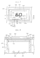
Fig. 1] Fig. 1 is a front view of a liquid crystal display device according to an embodiment of the present invention. - [
Fig. 2] Fig. 2 is a sectional view taken along a line A-A ofFig. 1 . - [
Fig. 3] Fig. 3 is a magnified sectional view of a liquid crystal display element inFig. 2 . - [
Fig. 4] Fig. 4 is a front view of a lower glass substrate provided with first and second lead terminals, the lead terminals of the same embodiment. - [
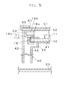
Fig. 5] Fig. 5 is a sectional view taken along a line C-C ofFig. 1 . - [
Fig. 6] Fig. 6 is a sectional view taken along a line D-D ofFig. 1 . - [
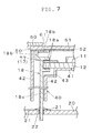
Fig. 7] Fig. 7 is a sectional view showing essential parts of a liquid crystal display device according to a modification of the same embodiment. - Hereinafter, an explanation will be given of an embodiment of the present invention applied to a digital speed meter installed in a vehicle instrument, for example, with reference to the
Fig. 1 to Fig. 6 . - In
Fig. 1 and Fig. 2 , a digital speed meter as a liquid crystal display device according to the embodiment comprises a liquidcrystal display element 10, acircuit board 20 that is disposed behind the liquidcrystal display element 10 and is conductively connected to the liquidcrystal display element 10 through alead terminal 16 that is a connection member to be described later, alight source 30 mounted on thecircuit board 20, acase body 40 disposed between the liquidcrystal display element 10 andcircuit board 20, a display panel (a front panel) 50 disposed in front of the liquidcrystal display element 10 so as to cover the liquidcrystal display element 10, and aflap member 60 to cover a peripheral edge of thedisplay panel 50. - As shown in
Fig. 3 , the liquidcrystal display element 10 is configured to connect the peripheries of theupper insulting substrate 11 and lowerinsulating substrate 12 with a sealingmaterial 13, and to seal aliquid crystal 14 between theinsulating substrates material 13. Theinsulating substrates insulating substrate 11, and a lower polarizing plate (not shown) is provided on the lower surface of the lowerinsulating substrate 12. - A first transparent electrode 11a that is a transparent electrode having a predetermined shape is provided on the inside surface of the upper insulating substrate 11 (namely, on the surface of the upper
insulating substrate 11 opposing the lower insulating substrate 12). A second transparent electrode 12a that is a transparent electrode having a predetermined shape is provided on the inside surface of the lower insulating substrate 12 (namely, on the surface of the lowerinsulating substrate 12 opposing the upper insulating substrate 11) so as to oppose (correspond to) the first transparent electrode 11a. - The first transparent electrode 11a and second transparent electrode 12a are arranged on the inside surfaces of the
insulating substrates liquid crystal 14. The planar shapes of the transparent electrodes seem substantially the same from a viewer (when looking straight at the liquid crystal display device). The portions of the display surface area of the liquidcrystal display element 10 corresponding to the first transparent electrode 11a and second transparent electrode 12a form adisplay portion 15 that forms a display pattern. In other words, this means that thedisplay portion 15 is formed by providing the transparent electrodes 11a and 12a on the inside surfaces of theinsulating substrates - Of the upper
insulating substrate 11 and lowerinsulating substrate 12, in the lowerinsulating substrate 12, a plurality ofmetal lead terminals 16 is fixed so as to along one end edge. In this embodiment, eachlead terminal 16 is centrally provided in a part of one end edge of the lowerinsulating substrate 12, thereby conductively connecting the liquidcrystal display element 10 andcircuit board 20. - Although a detailed illustration is omitted, the shape of each
lead terminal 16 is substantially the same as the shape of a second lead terminal to be described later. Thelead terminal 16 has a holding part and a lead portion. The holding part of thelead terminal 16 is formed in a U-shape, and is electrically connected to the second transparent electrode 12a when it holds the end of the lowerinsulating substrate 12. The end portion of thelead terminal 16 is electrically connected to a wiring (not shown) provided in thecircuit board 20. - When a voltage corresponding to an external measurand is applied across the transparent electrodes 11a and 12a through the
lead terminal 16, a measurand (for example, a vehicle speed) corresponding to a vehicle operating state is digitally displayed black in thedisplay portion 15. In the liquidcrystal display element 10, the background area 15a except thedisplay portion 15 is illuminated by lighting of thelight source 30 mounted on thecircuit board 20. - Of the
insulating substrates insulating substrate 12, aconductive part 17 comprising a substantially frame-shaped conductive pattern is formed so as to surround the second transparent electrode 12a. Theconductive part 17 is formed in a substantially frame shape on the inside surface of the lowerinsulating substrate 12 so as to avoid the disposed position of the lead terminal 16 (seeFig. 4 ). InFig. 4 , the transparent electrode 12a is formed inside the conductive part 17 (in the substantially central area of the lower insulating substrate 12), but an illustration of the transparent electrode 12a is omitted. - In particular, the
conductive part 17 comprises a first conductive pattern T1 whose one end side is conductively connected to a first grounding terminal to be described later and the other end side is located between the first grounding terminal and transparent electrode 12a, a second conductive pattern T2 that is formed by routing from the first conductive pattern T1 opposite to the part connected to the first grounding terminal to the right side of the lowerinsulating substrate 12, a third conductive pattern T3 that is formed by routing along the right end surface of the lowerinsulating substrate 12, a fourth conductive pattern T4 that is formed by routing along the upper end surface of the lowerinsulating substrate 12, a fifth conductive pattern T5 that is formed by routing along the left end surface of the lowerinsulating substrate 12, a sixth conductive pattern T6 that extends from the lower end of the fifth conductive pattern T5 toward the second conductive pattern T2 without contacting the second conductive pattern T2, and a seventh conductive pattern T7 that conductively connects the sixth conductive pattern T6 and second grounding terminal to be described later. - Further, on the right side of each
lead terminal 16, afirst grounding terminal 18 that is a first grounding part is provided in the lower insulating substrate 12 a state of being juxtaposed with eachlead terminal 16. Thefirst grounding terminal 18 is made of metal material like eachlead terminal 16, and has a holding part 18a conductively connected to the first conductive pattern T1 of theconductive part 17, and acontact piece 18b formed by bending in a substantially U-shape (seeFig. 5 ). - The holding part 18a is formed in a substantially U-shape, and is electrically connected to the first conductive pattern T1 by holding the end of the lower
insulating substrate 12. On the other hand, thecontact piece 18b is configured so that its distal end side contacts (abuts) the back of a display panel 50 (a ground color part 52), and has a function of propagating static electricity charged in thedisplay panel 50 to the conductive part 17 (the first conductive pattern T1) through the holding part 18a of thefirst grounding terminal 18. - In other words, in this embodiment, the
first grounding terminal 18 is configured so that one end side that is the holding part 18a is conductively connected to the first conductive pattern T1 of theconductive part 17, and the other end side that is a front end of thecontact piece 18b abuts thedisplay panel 50. - On the other hand, on the left side of each
lead terminal 16 that is the opposite side to thefirst grounding terminal 18, thesecond grounding terminal 19 that is the second grounding part is provided in the lower insulating substrate 12 a state of being juxtaposed with eachlead terminal 16. Thesecond grounding terminal 19 is made of metal material like eachlead terminal 16 andfirst lead terminal 18, and has a holding part 19a of the same shape as the holding part 18a of thefirst grounding terminal 18, and alinear lead part 19b formed by suspending downward the holding part 19a (namely, toward the circuit board 20) (seeFig. 6 ). - The holding part 19a is formed in a substantially U-shape, and is electrically connected to the seventh conductive pattern T7 of the
conductive part 17 by holding the end of the lowerinsulating substrate 12. On the other hand, the front end of thelead part 19b that is located opposite to the holding part 19a is electrically connected to a grounding part to be described later provided in thecircuit board 20. - In other words, in this embodiment, the
second grounding terminal 19 is configured so that one end side that is the holding part 19a is conductively connected to the seventh conductive pattern T7 of theconductive part 17, and the other end that is a front end of thelead part 19b is conductively connected to the grounding part. - Therefore, when the
display panel 50 electrostatically charged, the static electricity charged in thedisplay panel 50 propagates to the conductive part 17 (namely, propagates sequentially to the first to seventh conductive patterns T1 to T7) through thecontact piece 18b and holding part 18a of thefirst grounding terminal 18, and then flows to the grounding part provided in thecircuit board 20 through the holding part 19a andlead part 19b of thesecond grounding terminal 19 that is conductively connected to the seventh conductive pattern T7 (seeFig. 4 to Fig. 6 ). - The
circuit board 20 is made of a rigid circuit board provided with a wiring pattern that is the wiring part formed on a glass epoxy resin base material, for example, in which the wiring part is conductively connected to alight source 30, an element driving circuit (not shown) to drive the liquidcrystal display element 10, and various circuit components such as a resistor and a capacitor (not shown). - A
reference numeral 21 denotes a grounding part comprising a grounding pattern provided on the front surface of thecircuit board 20. The groundingpart 21 is conductively connected to thelead part 19b of thesecond grounding terminal 19. In this case, ahole 22 penetrating the front and back of thecircuit board 20 is provided at a portion of thecircuit board 20 corresponding to thelead part 19b, and the front end of thelead part 19b penetrates through thehole 22, and projects to the back of thecircuit board 20. In other words, the groundingpart 21 is formed as a pattern on the front (or back) of thecircuit board 20 that is a periphery of thehole 22, and is electrically connected to thelead part 19b by soldering or the like. - The
light source 30 is comprised of a chip type light-emitting diode to emit an appropriate color, for example, and is comprised of a light-emitting body, which is mounted on the wiring part provided on thecircuit board 20, and supplies illumination light to the liquidcrystal display element 10. The illumination light from thelight source 30 illuminates the background area 15a except thedisplay portion 15 by transmitting through there. - The
case body 40 is made of white synthetic resin, for example, and has a function as a supporter to support the liquidcrystal display element 10 anddisplay panel 50, a function as a reflector to reflect the illumination light from thelight source 30 to the liquidcrystal display element 10, and a function as a terminal holder to guide and hold eachlead terminal 16 andsecond grounding terminal 19. - Such a
case body 40 comprises a substantially frame-shapedbase part 41 to support the liquidcrystal display element 10 anddisplay panel 50, a plurality ofterminal holders 42 to guide and hold eachlead terminal 16 andsecond grounding terminal 19, and aconnection part 43 to connect thebase part 41 andterminal guide 42, which are formed in one body. - Each
terminal holder 42 is formed substantially in a frame shape, and is configured to guide the lead part of eachlead terminal 16 and thelead part 19b of thesecond grounding terminal 19.Fig. 6 shows only theterminal holder 42 corresponding to thelead part 19b of thesecond grounding terminal 19. It is needless to say that theterminal holder 42 corresponding to the lead part of eachlead terminal 16 has the same shape as thelead part 19b. - The
display panel 50 comprises a design panel provided with a display design such as an indicator display portion (not shown), and uses a light-transmissive substrate 51 made of polycarbonate as a base material. On the back of the light-transmissive substrate 51, aground color part 52 made of a blacked print layer is formed by printing using a means of screen printing, etc. - In this case, in the central area of the
ground color part 52 corresponding to thedisplay portion 15 of the liquidcrystal display element 10, a substantially rectangular throughportion 53, which is a vent print part where the black printed layer forming theground color part 52 is not formed, is provided. Therefore, when a viewer looks straight at the liquid crystal display device from the front side of the liquid crystal display device, a viewer can see (visually recognize) display of thedisplay portion 15 of the liquidcrystal display element 10 through the throughportion 53 provided in thedisplay panel 50. - Further, in this case, a clearance between the through
portion 53 formed in the central area of thedisplay panel 50 and the liquid crystal display element 10 (the upper insulating substrate 11) disposed behind the display panel 50 (the through portion 53) so as to be parallel to thedisplay panel 50 should be set to several millimeters. Thebase color part 52 may be formed by printing on the front surface of the light-transmissive substrate 51, not on the back of the light-transmissive substrate 51, or thedisplay panel 50 may be formed as a panel body not provided with the display design. Further, if necessary, a diffusing plate (not shown) for evenly diffusing the illumination light from thelight source 30 may be provided between thedisplay panel 50 andcircuit board 20. - The
flap member 60 is made of black synthetic resin, for example, and is disposed on thedisplay panel 50 so as to cover essential parts of thedisplay panel 50, and is provided with anopening 61 comprised of an open window corresponding to the throughportion 53. - The liquid crystal display device comprises the parts described above. In such a configuration, static electricity charged on the display panel 50 (the light-transmissive substrate 51) when a human hand touches the area near the center of the front surface of the through
portion 53 of thedisplay panel 50, for example, sequentially propagates to thecontact piece 18b abutting thedisplay panel 50 and the holding part 18a of thefirst grounding terminal 18, the first conductive pattern T1 that is a predetermined portion of theconductive part 17, second conductive pattern T2, third conductive pattern T3, fourth conductive pattern T4, fifth conductive pattern T5 and sixth conductive pattern T6, which are predetermined parts of theconductive part 17, the seventh conductive pattern T7 that is the other portion of theconductive part 17 different from the predetermined portion, and the holding part 19a andlead part 19b of thesecond grounding terminal 19, and then positively flows finally to thegrounding part 21 that is a grounding pattern of thecircuit board 20 conductively connected to thelead part 19b. This suppresses the element driving circuit from being damaged by static electricity, and eliminates the possibility of malfunction (display error) of the liquidcrystal display element 10 under the influence of static electricity, thereby providing a liquid crystal display device with improved display quality. - As described above, in this embodiment, a liquid crystal display device comprises a liquid
crystal display element 10 that forms adisplay portion 15 by providing transparent electrodes 11a and 12a on the inside surface of a pair of insulatingsubstrates liquid crystal 14, acircuit board 20 that is conductively connected to the liquidcrystal display element 10 through a plurality ofmetal lead terminals 16, and aconductive part 17 formed so as to surround the transparent electrode 12a, wherein the theconductive part 17 is provided on one insulatingsubstrate 12 so as to avoid a disposed position of thelead terminal 16, the liquid crystal display device comprising adisplay panel 50 having an throughportion 53 that enables visual recognition of thedisplay portion 15, afirst grounding terminal 18 whose one end side is conductively connected to a first conductive pattern T1 of theconductive part 17 and the other end side abuts thedisplay panel 50, and asecond grounding terminal 19 whose one end side is conductively connected to a conductive pattern T7 of theconductive part 17 and the other end side is conductively connected to agrounding part 21 provided on thecircuit board 20. A plurality oflead terminals 16 that are connecting members is provided on the lower insulatingsubstrate 12 so as to conductively connect the liquidcrystal display element 10 andcircuit board 20, and thesecond grounding terminals substrate 12 in a state of being juxtaposed with eachlead terminal 16. - Therefore, static electricity charged in the
display panel 50 when a human hand touches the area near the center of the front surface of the throughportion 53 propagates to thecontact piece 18b contacting (abutting) the display panel of thefirst grounding terminal 18 without propagating to the liquidcrystal display element 10, and the static electricity propagated to thecontact piece 18b propagates to theconductive part 17 comprised of conductive patterns and formed so as to surround thedisplay portion 15 through the holding part 18a. And, the static electricity propagated to theconductive part 17 positively flows finally to thegrounding part 21 comprised of grounding patterns and conductively connected to thelead part 19b through the holding part 19a andlead part 19b of thesecond grounding terminal 19 conductively connected to theconductive part 17. This eliminates the possibility of malfunction of the liquidcrystal display element 10 under the influence of static electricity, thereby providing a liquid crystal display device with improved display quality. - Further, in this embodiment, an explanation has been given of the aspect that the
contact piece 18b located in the other end side of thefirst grounding terminal 18 is formed by bending in a U-shape so as to abut thedisplay panel 50. However, thecontact piece 18b can be formed in any shape able to contact (abut) thedisplay panel 50, for example, thecontact piece 18b can be formed in a spiral (helical) shape or in zigzag (S-shape). - Further, the
contact piece 18b located in the other end side of thefirst grounding terminal 18 is desirably configured to always abut thedisplay panel 50 in a state of having elasticity to give a tension (a pressing elastic force) to the display panel. As thecontact piece 18b abuts thedisplay panel 50 in a state of having elasticity, the connection reliability between thefirst grounding terminal 18 anddisplay panel 50 can be improved. - Further, in this embodiment, an explanation has been given of the aspect that the through
portion 53 that enables viewing of thedisplay portion 15 is formed in a part of thedisplay panel 50 corresponding to thedisplay portion 15. However, though a detailed illustration is omitted, it may be permitted to provide a penetrated portion consisting of a substantially rectangular through-hole in a part of the display panel 50 (namely, a part of the light-transmissive substrate 51) corresponding to thedisplay portion 15, thereby enabling a viewer to visually recognize the display of thedisplay portion 15 through the penetrated portion. At this time, theground color part 52 may be provided in the back (or the front) of the light-transmissive substrate 51 except the penetrated portion. - Further, in this embodiment, an explanation has been given of the aspect that the
first grounding terminal 18 is comprised of a holding part 18a, and acontact piece 18b. However, as shown inFig. 7 illustrating a modification of the embodiment, thefirst grounding terminal 18 may be comprised of a holding part 18a, acontact piece 18, and a linear connection part 18c that is formed by suspending downward the holding part 18a close to thecircuit board 20, and the connection part 18c may be conductively connected to thegrounding part 21. - The present invention is applicable to a liquid crystal display device comprising a liquid crystal display element that forms a display portion by providing transparent electrodes on the inside surface of a pair of insulating substrates sealing a liquid crystal, and a circuit board that is conductively connected to the liquid crystal display element through a connection member comprised of a lead terminal.
-
- 10 Liquid crystal display element
- 11 Upper insulating substrate (Insulating substrate)
- 11a First transparent electrode (Transparent electrode)
- 12 Lower insulating substrate (Insulating substrate)
- 12a Second transparent electrode (Transparent electrode)
- 14 Liquid crystal
- 15 Display portion
- 16 Lead terminal (Connection member)
- 17 Conductive part
- 18 First grounding terminal (First grounding part)
- 18a, 19b Holding part
- 18b Contact piece
- 18c Connection part
- 19 Second grounding terminal (Second grounding part)
- 19b Lead part
- 20 Circuit board
- 21 Grounding part
- 40 Case body
- 50 Display panel (Front panel)
- 51 Light-transmissive substrate
- 53 Through portion
- 60 Flap member
- T1 First conductive pattern (Predetermined portion of conductive part)
- T2 Second conductive pattern
- T3 Third conductive pattern
- T4 Fourth conductive pattern
- T5 Fifth conductive pattern
- T6 Sixth conductive pattern
- T7 Seventh conductive pattern (Other portion of conductive part)
Claims (4)
- A liquid crystal display device comprising:a liquid crystal display element that forms a display portion by providing a transparent electrode on an inside surface of a pair of insulating substrates sealing a liquid crystal;a circuit board that is conductively connected to the liquid crystal display element through a predetermined connection member; anda conductive part that is formed so as to surround the transparent electrodes, whereinthe conductive part is provided on one of the pair of insulating substrates so as to avoid a disposed position of the connection member,the liquid crystal display device comprising:a front panel having a through portion or a penetrated portion that enables visual recognition of the display portion,a first grounding part whose one end side is conductively connected to a predetermined portion of the conductive part, and the other end side abuts the front panel; anda second grounding part whose one end side is conductively connected to the other portion of the conductive part different from the predetermined portion, and the other end side is conductively connected to a grounding part provided on the circuit board.
- The liquid crystal display device according to claim 1, wherein:the connection member comprises a plurality of lead terminals provided on one of the insulating substrates so as to conductively connect the liquid crystal display element and the circuit board, andthe first and second grounding parts comprise first and second grounding terminals provided on one of the insulating substrates in a state of being juxtaposed with the lead terminal.
- The liquid crystal display device according to claim 1 or claim 2, wherein the other end side of the first grounding part abuts the front panel in a state of having elasticity.
- The liquid crystal display device according to any one of claim 1 to claim 3, wherein the first grounding part is provided with a connection part that is conductively connected to the grounding part.
Applications Claiming Priority (2)
| Application Number | Priority Date | Filing Date | Title |
|---|---|---|---|
| JP2011014975A JP5590403B2 (en) | 2011-01-27 | 2011-01-27 | Liquid crystal display |
| PCT/JP2012/050450 WO2012102087A1 (en) | 2011-01-27 | 2012-01-12 | Liquid crystal display device |
Publications (3)
| Publication Number | Publication Date |
|---|---|
| EP2669733A1 true EP2669733A1 (en) | 2013-12-04 |
| EP2669733A4 EP2669733A4 (en) | 2014-08-20 |
| EP2669733B1 EP2669733B1 (en) | 2017-06-28 |
Family
ID=46580660
Family Applications (1)
| Application Number | Title | Priority Date | Filing Date |
|---|---|---|---|
| EP12739657.0A Not-in-force EP2669733B1 (en) | 2011-01-27 | 2012-01-12 | Liquid crystal display device |
Country Status (6)
| Country | Link |
|---|---|
| US (1) | US9411202B2 (en) |
| EP (1) | EP2669733B1 (en) |
| JP (1) | JP5590403B2 (en) |
| KR (1) | KR20140006824A (en) |
| CN (1) | CN103329031B (en) |
| WO (1) | WO2012102087A1 (en) |
Families Citing this family (4)
| Publication number | Priority date | Publication date | Assignee | Title |
|---|---|---|---|---|
| JP6120064B2 (en) * | 2013-04-09 | 2017-04-26 | 日本精機株式会社 | Display device |
| JP6493750B2 (en) * | 2015-04-22 | 2019-04-03 | 日本精機株式会社 | Instrument device |
| JP6837103B2 (en) * | 2019-08-08 | 2021-03-03 | 日本精機株式会社 | Vehicle display device |
| US11363745B1 (en) * | 2020-07-07 | 2022-06-14 | Waymo Llc | Housing for display electromagnetic shielding and electrostatic grounding |
Family Cites Families (28)
| Publication number | Priority date | Publication date | Assignee | Title |
|---|---|---|---|---|
| JPS5622468A (en) * | 1979-08-01 | 1981-03-03 | Nissan Motor | Liquid crystal display unit |
| JP2916824B2 (en) * | 1991-05-31 | 1999-07-05 | アルプス電気株式会社 | Liquid crystal display |
| JPH07152019A (en) * | 1993-11-30 | 1995-06-16 | Matsushita Electric Ind Co Ltd | Liquid crystal display |
| TW505801B (en) * | 1995-10-12 | 2002-10-11 | Hitachi Ltd | In-plane field type liquid crystal display device comprising a structure prevented from charging with electricity |
| US6532053B2 (en) * | 1996-12-18 | 2003-03-11 | Hitachi, Ltd. | Transverse electric field system liquid crystal display device suitable for improving aperture ratio |
| JPH10282896A (en) * | 1997-04-07 | 1998-10-23 | Mitsubishi Electric Corp | Display device |
| JPH11185991A (en) * | 1997-12-25 | 1999-07-09 | Casio Comput Co Ltd | Electronics |
| JP2000181362A (en) * | 1998-12-17 | 2000-06-30 | Alps Electric Co Ltd | Liquid crystal display device |
| JP3107078B2 (en) * | 1999-02-26 | 2000-11-06 | 日本電気株式会社 | Liquid crystal display |
| DE60014829D1 (en) * | 1999-05-21 | 2004-11-18 | Citizen Watch Co Ltd | Liquid crystal display panel |
| JP2001147441A (en) * | 1999-11-19 | 2001-05-29 | Nec Corp | Transverse electric field liquid crystal display device |
| JP2004233890A (en) * | 2003-01-31 | 2004-08-19 | Optrex Corp | Liquid crystal display device and discharging method for same |
| CN1292300C (en) * | 2003-04-29 | 2006-12-27 | 明基电通股份有限公司 | Electronic device and anti-static discharge method thereof |
| KR101107982B1 (en) * | 2004-08-19 | 2012-01-25 | 삼성전자주식회사 | Flat Panel Display |
| JP4667831B2 (en) * | 2004-11-12 | 2011-04-13 | パナソニック株式会社 | Communication terminal |
| JP4892946B2 (en) * | 2005-12-08 | 2012-03-07 | エプソンイメージングデバイス株式会社 | Electro-optical device and electronic apparatus |
| JP2007328922A (en) * | 2006-06-06 | 2007-12-20 | Sharp Corp | Electronics |
| US8400599B2 (en) * | 2006-08-16 | 2013-03-19 | Samsung Display Co., Ltd. | Liquid crystal display panel having a light blocking electrode |
| JP5000243B2 (en) * | 2006-09-08 | 2012-08-15 | 京セラ株式会社 | Electronics |
| KR20080023466A (en) * | 2006-09-11 | 2008-03-14 | 삼성에스디아이 주식회사 | Flat panel display |
| JP2008170812A (en) | 2007-01-12 | 2008-07-24 | Matsushita Electric Works Ltd | Liquid crystal display element |
| JP2009175709A (en) * | 2007-12-27 | 2009-08-06 | Seiko Instruments Inc | Display device |
| JP5283255B2 (en) * | 2008-02-14 | 2013-09-04 | 株式会社ジャパンディスプレイ | Liquid crystal display |
| TWI376544B (en) | 2008-06-16 | 2012-11-11 | Wintek Corp | Liquid crystal display panel |
| JP5311018B2 (en) * | 2008-12-23 | 2013-10-09 | 日本精機株式会社 | Liquid crystal display |
| JP5079715B2 (en) | 2009-01-16 | 2012-11-21 | 株式会社ジャパンディスプレイウェスト | Liquid crystal display |
| JP5690178B2 (en) * | 2010-04-26 | 2015-03-25 | 京セラディスプレイ株式会社 | Liquid crystal display |
| KR20120097146A (en) * | 2011-02-24 | 2012-09-03 | 엘지디스플레이 주식회사 | Liquid crystal display device |
-
2011
- 2011-01-27 JP JP2011014975A patent/JP5590403B2/en active Active
-
2012
- 2012-01-12 EP EP12739657.0A patent/EP2669733B1/en not_active Not-in-force
- 2012-01-12 US US13/982,241 patent/US9411202B2/en not_active Expired - Fee Related
- 2012-01-12 WO PCT/JP2012/050450 patent/WO2012102087A1/en not_active Ceased
- 2012-01-12 CN CN201280006300.XA patent/CN103329031B/en not_active Expired - Fee Related
- 2012-01-12 KR KR1020137018662A patent/KR20140006824A/en not_active Ceased
Also Published As
| Publication number | Publication date |
|---|---|
| EP2669733A4 (en) | 2014-08-20 |
| CN103329031A (en) | 2013-09-25 |
| JP5590403B2 (en) | 2014-09-17 |
| JP2012155176A (en) | 2012-08-16 |
| KR20140006824A (en) | 2014-01-16 |
| US9411202B2 (en) | 2016-08-09 |
| EP2669733B1 (en) | 2017-06-28 |
| CN103329031B (en) | 2016-01-20 |
| US20130314657A1 (en) | 2013-11-28 |
| WO2012102087A1 (en) | 2012-08-02 |
Similar Documents
| Publication | Publication Date | Title |
|---|---|---|
| CN101430473B (en) | Display device and timepiece | |
| JP5845952B2 (en) | Display device | |
| JP6201321B2 (en) | Display device | |
| US9411202B2 (en) | Liquid crystal display device | |
| CN103091900A (en) | Liquid crystal display device | |
| CN105074803B (en) | Display device | |
| JP5207135B2 (en) | Instrument device | |
| JP5621647B2 (en) | Liquid crystal display | |
| JP6048061B2 (en) | Liquid crystal display | |
| US20210103351A1 (en) | Display device | |
| JP6493750B2 (en) | Instrument device | |
| US10725232B2 (en) | Backlight device and liquid crystal display device comprising the same | |
| JP5510391B2 (en) | Electrical circuit device | |
| EP3581996B1 (en) | Image display device | |
| JP2012189666A (en) | Display device | |
| JP2011257654A (en) | Liquid crystal display device | |
| JP2012153281A (en) | Display device | |
| JPH027071B2 (en) | ||
| JP5513812B2 (en) | Display device | |
| JP5310288B2 (en) | Liquid crystal display | |
| JP2010151852A (en) | Liquid crystal display | |
| JP2019006171A (en) | Display device | |
| JP6790748B2 (en) | Instrument device | |
| JP2019002984A (en) | Display device | |
| JP2021051120A (en) | Display device |
Legal Events
| Date | Code | Title | Description |
|---|---|---|---|
| PUAI | Public reference made under article 153(3) epc to a published international application that has entered the european phase |
Free format text: ORIGINAL CODE: 0009012 |
|
| 17P | Request for examination filed |
Effective date: 20130715 |
|
| AK | Designated contracting states |
Kind code of ref document: A1 Designated state(s): AL AT BE BG CH CY CZ DE DK EE ES FI FR GB GR HR HU IE IS IT LI LT LU LV MC MK MT NL NO PL PT RO RS SE SI SK SM TR |
|
| DAX | Request for extension of the european patent (deleted) | ||
| A4 | Supplementary search report drawn up and despatched |
Effective date: 20140721 |
|
| RIC1 | Information provided on ipc code assigned before grant |
Ipc: G02F 1/1343 20060101ALI20140715BHEP Ipc: G02F 1/1333 20060101AFI20140715BHEP Ipc: G02F 1/1345 20060101ALI20140715BHEP |
|
| 17Q | First examination report despatched |
Effective date: 20150930 |
|
| GRAP | Despatch of communication of intention to grant a patent |
Free format text: ORIGINAL CODE: EPIDOSNIGR1 |
|
| INTG | Intention to grant announced |
Effective date: 20170110 |
|
| GRAS | Grant fee paid |
Free format text: ORIGINAL CODE: EPIDOSNIGR3 |
|
| GRAA | (expected) grant |
Free format text: ORIGINAL CODE: 0009210 |
|
| AK | Designated contracting states |
Kind code of ref document: B1 Designated state(s): AL AT BE BG CH CY CZ DE DK EE ES FI FR GB GR HR HU IE IS IT LI LT LU LV MC MK MT NL NO PL PT RO RS SE SI SK SM TR |
|
| REG | Reference to a national code |
Ref country code: GB Ref legal event code: FG4D |
|
| REG | Reference to a national code |
Ref country code: CH Ref legal event code: EP |
|
| REG | Reference to a national code |
Ref country code: AT Ref legal event code: REF Ref document number: 905379 Country of ref document: AT Kind code of ref document: T Effective date: 20170715 |
|
| REG | Reference to a national code |
Ref country code: IE Ref legal event code: FG4D |
|
| REG | Reference to a national code |
Ref country code: DE Ref legal event code: R096 Ref document number: 602012033958 Country of ref document: DE |
|
| PG25 | Lapsed in a contracting state [announced via postgrant information from national office to epo] |
Ref country code: GR Free format text: LAPSE BECAUSE OF FAILURE TO SUBMIT A TRANSLATION OF THE DESCRIPTION OR TO PAY THE FEE WITHIN THE PRESCRIBED TIME-LIMIT Effective date: 20170929 Ref country code: NO Free format text: LAPSE BECAUSE OF FAILURE TO SUBMIT A TRANSLATION OF THE DESCRIPTION OR TO PAY THE FEE WITHIN THE PRESCRIBED TIME-LIMIT Effective date: 20170928 Ref country code: LT Free format text: LAPSE BECAUSE OF FAILURE TO SUBMIT A TRANSLATION OF THE DESCRIPTION OR TO PAY THE FEE WITHIN THE PRESCRIBED TIME-LIMIT Effective date: 20170628 Ref country code: FI Free format text: LAPSE BECAUSE OF FAILURE TO SUBMIT A TRANSLATION OF THE DESCRIPTION OR TO PAY THE FEE WITHIN THE PRESCRIBED TIME-LIMIT Effective date: 20170628 Ref country code: HR Free format text: LAPSE BECAUSE OF FAILURE TO SUBMIT A TRANSLATION OF THE DESCRIPTION OR TO PAY THE FEE WITHIN THE PRESCRIBED TIME-LIMIT Effective date: 20170628 |
|
| REG | Reference to a national code |
Ref country code: NL Ref legal event code: MP Effective date: 20170628 |
|
| REG | Reference to a national code |
Ref country code: LT Ref legal event code: MG4D |
|
| REG | Reference to a national code |
Ref country code: AT Ref legal event code: MK05 Ref document number: 905379 Country of ref document: AT Kind code of ref document: T Effective date: 20170628 |
|
| PG25 | Lapsed in a contracting state [announced via postgrant information from national office to epo] |
Ref country code: RS Free format text: LAPSE BECAUSE OF FAILURE TO SUBMIT A TRANSLATION OF THE DESCRIPTION OR TO PAY THE FEE WITHIN THE PRESCRIBED TIME-LIMIT Effective date: 20170628 Ref country code: SE Free format text: LAPSE BECAUSE OF FAILURE TO SUBMIT A TRANSLATION OF THE DESCRIPTION OR TO PAY THE FEE WITHIN THE PRESCRIBED TIME-LIMIT Effective date: 20170628 Ref country code: BG Free format text: LAPSE BECAUSE OF FAILURE TO SUBMIT A TRANSLATION OF THE DESCRIPTION OR TO PAY THE FEE WITHIN THE PRESCRIBED TIME-LIMIT Effective date: 20170928 Ref country code: LV Free format text: LAPSE BECAUSE OF FAILURE TO SUBMIT A TRANSLATION OF THE DESCRIPTION OR TO PAY THE FEE WITHIN THE PRESCRIBED TIME-LIMIT Effective date: 20170628 Ref country code: NL Free format text: LAPSE BECAUSE OF FAILURE TO SUBMIT A TRANSLATION OF THE DESCRIPTION OR TO PAY THE FEE WITHIN THE PRESCRIBED TIME-LIMIT Effective date: 20170628 |
|
| REG | Reference to a national code |
Ref country code: FR Ref legal event code: PLFP Year of fee payment: 7 |
|
| PG25 | Lapsed in a contracting state [announced via postgrant information from national office to epo] |
Ref country code: RO Free format text: LAPSE BECAUSE OF FAILURE TO SUBMIT A TRANSLATION OF THE DESCRIPTION OR TO PAY THE FEE WITHIN THE PRESCRIBED TIME-LIMIT Effective date: 20170628 Ref country code: CZ Free format text: LAPSE BECAUSE OF FAILURE TO SUBMIT A TRANSLATION OF THE DESCRIPTION OR TO PAY THE FEE WITHIN THE PRESCRIBED TIME-LIMIT Effective date: 20170628 Ref country code: SK Free format text: LAPSE BECAUSE OF FAILURE TO SUBMIT A TRANSLATION OF THE DESCRIPTION OR TO PAY THE FEE WITHIN THE PRESCRIBED TIME-LIMIT Effective date: 20170628 Ref country code: EE Free format text: LAPSE BECAUSE OF FAILURE TO SUBMIT A TRANSLATION OF THE DESCRIPTION OR TO PAY THE FEE WITHIN THE PRESCRIBED TIME-LIMIT Effective date: 20170628 Ref country code: AT Free format text: LAPSE BECAUSE OF FAILURE TO SUBMIT A TRANSLATION OF THE DESCRIPTION OR TO PAY THE FEE WITHIN THE PRESCRIBED TIME-LIMIT Effective date: 20170628 |
|
| PG25 | Lapsed in a contracting state [announced via postgrant information from national office to epo] |
Ref country code: IS Free format text: LAPSE BECAUSE OF FAILURE TO SUBMIT A TRANSLATION OF THE DESCRIPTION OR TO PAY THE FEE WITHIN THE PRESCRIBED TIME-LIMIT Effective date: 20171028 Ref country code: SM Free format text: LAPSE BECAUSE OF FAILURE TO SUBMIT A TRANSLATION OF THE DESCRIPTION OR TO PAY THE FEE WITHIN THE PRESCRIBED TIME-LIMIT Effective date: 20170628 Ref country code: IT Free format text: LAPSE BECAUSE OF FAILURE TO SUBMIT A TRANSLATION OF THE DESCRIPTION OR TO PAY THE FEE WITHIN THE PRESCRIBED TIME-LIMIT Effective date: 20170628 Ref country code: ES Free format text: LAPSE BECAUSE OF FAILURE TO SUBMIT A TRANSLATION OF THE DESCRIPTION OR TO PAY THE FEE WITHIN THE PRESCRIBED TIME-LIMIT Effective date: 20170628 Ref country code: PL Free format text: LAPSE BECAUSE OF FAILURE TO SUBMIT A TRANSLATION OF THE DESCRIPTION OR TO PAY THE FEE WITHIN THE PRESCRIBED TIME-LIMIT Effective date: 20170628 |
|
| REG | Reference to a national code |
Ref country code: DE Ref legal event code: R097 Ref document number: 602012033958 Country of ref document: DE |
|
| PG25 | Lapsed in a contracting state [announced via postgrant information from national office to epo] |
Ref country code: DK Free format text: LAPSE BECAUSE OF FAILURE TO SUBMIT A TRANSLATION OF THE DESCRIPTION OR TO PAY THE FEE WITHIN THE PRESCRIBED TIME-LIMIT Effective date: 20170628 |
|
| PLBE | No opposition filed within time limit |
Free format text: ORIGINAL CODE: 0009261 |
|
| STAA | Information on the status of an ep patent application or granted ep patent |
Free format text: STATUS: NO OPPOSITION FILED WITHIN TIME LIMIT |
|
| 26N | No opposition filed |
Effective date: 20180329 |
|
| PG25 | Lapsed in a contracting state [announced via postgrant information from national office to epo] |
Ref country code: SI Free format text: LAPSE BECAUSE OF FAILURE TO SUBMIT A TRANSLATION OF THE DESCRIPTION OR TO PAY THE FEE WITHIN THE PRESCRIBED TIME-LIMIT Effective date: 20170628 |
|
| REG | Reference to a national code |
Ref country code: CH Ref legal event code: PL |
|
| PG25 | Lapsed in a contracting state [announced via postgrant information from national office to epo] |
Ref country code: LU Free format text: LAPSE BECAUSE OF NON-PAYMENT OF DUE FEES Effective date: 20180112 |
|
| REG | Reference to a national code |
Ref country code: IE Ref legal event code: MM4A |
|
| REG | Reference to a national code |
Ref country code: BE Ref legal event code: MM Effective date: 20180131 |
|
| PG25 | Lapsed in a contracting state [announced via postgrant information from national office to epo] |
Ref country code: LI Free format text: LAPSE BECAUSE OF NON-PAYMENT OF DUE FEES Effective date: 20180131 Ref country code: BE Free format text: LAPSE BECAUSE OF NON-PAYMENT OF DUE FEES Effective date: 20180131 Ref country code: CH Free format text: LAPSE BECAUSE OF NON-PAYMENT OF DUE FEES Effective date: 20180131 |
|
| PG25 | Lapsed in a contracting state [announced via postgrant information from national office to epo] |
Ref country code: IE Free format text: LAPSE BECAUSE OF NON-PAYMENT OF DUE FEES Effective date: 20180112 |
|
| PGFP | Annual fee paid to national office [announced via postgrant information from national office to epo] |
Ref country code: FR Payment date: 20181213 Year of fee payment: 8 |
|
| PGFP | Annual fee paid to national office [announced via postgrant information from national office to epo] |
Ref country code: GB Payment date: 20190109 Year of fee payment: 8 Ref country code: DE Payment date: 20190102 Year of fee payment: 8 |
|
| PG25 | Lapsed in a contracting state [announced via postgrant information from national office to epo] |
Ref country code: MC Free format text: LAPSE BECAUSE OF FAILURE TO SUBMIT A TRANSLATION OF THE DESCRIPTION OR TO PAY THE FEE WITHIN THE PRESCRIBED TIME-LIMIT Effective date: 20170628 |
|
| PG25 | Lapsed in a contracting state [announced via postgrant information from national office to epo] |
Ref country code: MT Free format text: LAPSE BECAUSE OF NON-PAYMENT OF DUE FEES Effective date: 20180112 |
|
| PG25 | Lapsed in a contracting state [announced via postgrant information from national office to epo] |
Ref country code: TR Free format text: LAPSE BECAUSE OF FAILURE TO SUBMIT A TRANSLATION OF THE DESCRIPTION OR TO PAY THE FEE WITHIN THE PRESCRIBED TIME-LIMIT Effective date: 20170628 |
|
| PG25 | Lapsed in a contracting state [announced via postgrant information from national office to epo] |
Ref country code: HU Free format text: LAPSE BECAUSE OF FAILURE TO SUBMIT A TRANSLATION OF THE DESCRIPTION OR TO PAY THE FEE WITHIN THE PRESCRIBED TIME-LIMIT; INVALID AB INITIO Effective date: 20120112 Ref country code: PT Free format text: LAPSE BECAUSE OF FAILURE TO SUBMIT A TRANSLATION OF THE DESCRIPTION OR TO PAY THE FEE WITHIN THE PRESCRIBED TIME-LIMIT Effective date: 20170628 |
|
| PG25 | Lapsed in a contracting state [announced via postgrant information from national office to epo] |
Ref country code: MK Free format text: LAPSE BECAUSE OF NON-PAYMENT OF DUE FEES Effective date: 20170628 Ref country code: CY Free format text: LAPSE BECAUSE OF FAILURE TO SUBMIT A TRANSLATION OF THE DESCRIPTION OR TO PAY THE FEE WITHIN THE PRESCRIBED TIME-LIMIT Effective date: 20170628 |
|
| PG25 | Lapsed in a contracting state [announced via postgrant information from national office to epo] |
Ref country code: AL Free format text: LAPSE BECAUSE OF FAILURE TO SUBMIT A TRANSLATION OF THE DESCRIPTION OR TO PAY THE FEE WITHIN THE PRESCRIBED TIME-LIMIT Effective date: 20170628 |
|
| REG | Reference to a national code |
Ref country code: DE Ref legal event code: R119 Ref document number: 602012033958 Country of ref document: DE |
|
| GBPC | Gb: european patent ceased through non-payment of renewal fee |
Effective date: 20200112 |
|
| PG25 | Lapsed in a contracting state [announced via postgrant information from national office to epo] |
Ref country code: DE Free format text: LAPSE BECAUSE OF NON-PAYMENT OF DUE FEES Effective date: 20200801 Ref country code: GB Free format text: LAPSE BECAUSE OF NON-PAYMENT OF DUE FEES Effective date: 20200112 Ref country code: FR Free format text: LAPSE BECAUSE OF NON-PAYMENT OF DUE FEES Effective date: 20200131 |