EP2669093A1 - Thermal head and thermal printer equipped with same - Google Patents
Thermal head and thermal printer equipped with same Download PDFInfo
- Publication number
- EP2669093A1 EP2669093A1 EP12738921.1A EP12738921A EP2669093A1 EP 2669093 A1 EP2669093 A1 EP 2669093A1 EP 12738921 A EP12738921 A EP 12738921A EP 2669093 A1 EP2669093 A1 EP 2669093A1
- Authority
- EP
- European Patent Office
- Prior art keywords
- substrate
- protection film
- heat
- edge
- disposed
- Prior art date
- Legal status (The legal status is an assumption and is not a legal conclusion. Google has not performed a legal analysis and makes no representation as to the accuracy of the status listed.)
- Granted
Links
- 239000000758 substrate Substances 0.000 claims abstract description 99
- 238000003860 storage Methods 0.000 claims abstract description 72
- 239000011521 glass Substances 0.000 claims abstract description 23
- VYPSYNLAJGMNEJ-UHFFFAOYSA-N Silicium dioxide Chemical compound O=[Si]=O VYPSYNLAJGMNEJ-UHFFFAOYSA-N 0.000 claims description 24
- 229910052681 coesite Inorganic materials 0.000 claims description 12
- 229910052906 cristobalite Inorganic materials 0.000 claims description 12
- 239000000377 silicon dioxide Substances 0.000 claims description 12
- 229910052682 stishovite Inorganic materials 0.000 claims description 12
- 229910052905 tridymite Inorganic materials 0.000 claims description 12
- 229920005989 resin Polymers 0.000 claims description 10
- 239000011347 resin Substances 0.000 claims description 10
- 229910052814 silicon oxide Inorganic materials 0.000 claims description 6
- 230000007246 mechanism Effects 0.000 claims description 5
- 239000010408 film Substances 0.000 description 101
- 238000000034 method Methods 0.000 description 22
- 239000000463 material Substances 0.000 description 18
- 230000008569 process Effects 0.000 description 10
- 238000007639 printing Methods 0.000 description 5
- XLOMVQKBTHCTTD-UHFFFAOYSA-N Zinc monoxide Chemical compound [Zn]=O XLOMVQKBTHCTTD-UHFFFAOYSA-N 0.000 description 4
- PNEYBMLMFCGWSK-UHFFFAOYSA-N aluminium oxide Inorganic materials [O-2].[O-2].[O-2].[Al+3].[Al+3] PNEYBMLMFCGWSK-UHFFFAOYSA-N 0.000 description 4
- 239000011248 coating agent Substances 0.000 description 4
- 238000000576 coating method Methods 0.000 description 4
- HTUMBQDCCIXGCV-UHFFFAOYSA-N lead oxide Chemical compound [O-2].[Pb+2] HTUMBQDCCIXGCV-UHFFFAOYSA-N 0.000 description 4
- YEXPOXQUZXUXJW-UHFFFAOYSA-N lead(II) oxide Inorganic materials [Pb]=O YEXPOXQUZXUXJW-UHFFFAOYSA-N 0.000 description 4
- 239000002184 metal Substances 0.000 description 4
- 229910052751 metal Inorganic materials 0.000 description 4
- 238000007650 screen-printing Methods 0.000 description 4
- 239000010409 thin film Substances 0.000 description 4
- 229910011255 B2O3 Inorganic materials 0.000 description 3
- 238000005299 abrasion Methods 0.000 description 3
- 230000007797 corrosion Effects 0.000 description 3
- 238000005260 corrosion Methods 0.000 description 3
- 229910052593 corundum Inorganic materials 0.000 description 3
- JKWMSGQKBLHBQQ-UHFFFAOYSA-N diboron trioxide Chemical compound O=BOB=O JKWMSGQKBLHBQQ-UHFFFAOYSA-N 0.000 description 3
- 238000004519 manufacturing process Methods 0.000 description 3
- 230000003647 oxidation Effects 0.000 description 3
- 238000007254 oxidation reaction Methods 0.000 description 3
- 238000000059 patterning Methods 0.000 description 3
- 230000004044 response Effects 0.000 description 3
- 238000004544 sputter deposition Methods 0.000 description 3
- 229910001845 yogo sapphire Inorganic materials 0.000 description 3
- RYGMFSIKBFXOCR-UHFFFAOYSA-N Copper Chemical compound [Cu] RYGMFSIKBFXOCR-UHFFFAOYSA-N 0.000 description 2
- 239000005062 Polybutadiene Substances 0.000 description 2
- 239000000853 adhesive Substances 0.000 description 2
- 230000001070 adhesive effect Effects 0.000 description 2
- 229910052782 aluminium Inorganic materials 0.000 description 2
- XAGFODPZIPBFFR-UHFFFAOYSA-N aluminium Chemical compound [Al] XAGFODPZIPBFFR-UHFFFAOYSA-N 0.000 description 2
- QVQLCTNNEUAWMS-UHFFFAOYSA-N barium oxide Inorganic materials [Ba]=O QVQLCTNNEUAWMS-UHFFFAOYSA-N 0.000 description 2
- WMWLMWRWZQELOS-UHFFFAOYSA-N bismuth(iii) oxide Chemical compound O=[Bi]O[Bi]=O WMWLMWRWZQELOS-UHFFFAOYSA-N 0.000 description 2
- ODINCKMPIJJUCX-UHFFFAOYSA-N calcium oxide Inorganic materials [Ca]=O ODINCKMPIJJUCX-UHFFFAOYSA-N 0.000 description 2
- 229910052802 copper Inorganic materials 0.000 description 2
- 239000010949 copper Substances 0.000 description 2
- 230000007547 defect Effects 0.000 description 2
- 230000006866 deterioration Effects 0.000 description 2
- 239000003822 epoxy resin Substances 0.000 description 2
- 238000010304 firing Methods 0.000 description 2
- 229920002857 polybutadiene Polymers 0.000 description 2
- 229920000647 polyepoxide Polymers 0.000 description 2
- 238000003825 pressing Methods 0.000 description 2
- 238000000926 separation method Methods 0.000 description 2
- 239000010935 stainless steel Substances 0.000 description 2
- 229910001220 stainless steel Inorganic materials 0.000 description 2
- BQCADISMDOOEFD-UHFFFAOYSA-N Silver Chemical compound [Ag] BQCADISMDOOEFD-UHFFFAOYSA-N 0.000 description 1
- 229910045601 alloy Inorganic materials 0.000 description 1
- 239000000956 alloy Substances 0.000 description 1
- QVGXLLKOCUKJST-UHFFFAOYSA-N atomic oxygen Chemical compound [O] QVGXLLKOCUKJST-UHFFFAOYSA-N 0.000 description 1
- 239000000919 ceramic Substances 0.000 description 1
- 238000006243 chemical reaction Methods 0.000 description 1
- 238000000151 deposition Methods 0.000 description 1
- 230000008021 deposition Effects 0.000 description 1
- 230000000694 effects Effects 0.000 description 1
- 239000012777 electrically insulating material Substances 0.000 description 1
- 238000005530 etching Methods 0.000 description 1
- PCHJSUWPFVWCPO-UHFFFAOYSA-N gold Chemical compound [Au] PCHJSUWPFVWCPO-UHFFFAOYSA-N 0.000 description 1
- 229910052737 gold Inorganic materials 0.000 description 1
- 239000010931 gold Substances 0.000 description 1
- CPLXHLVBOLITMK-UHFFFAOYSA-N magnesium oxide Inorganic materials [Mg]=O CPLXHLVBOLITMK-UHFFFAOYSA-N 0.000 description 1
- 239000007769 metal material Substances 0.000 description 1
- 150000002739 metals Chemical class 0.000 description 1
- 238000002156 mixing Methods 0.000 description 1
- 239000000203 mixture Substances 0.000 description 1
- 238000012986 modification Methods 0.000 description 1
- 230000004048 modification Effects 0.000 description 1
- 229910021421 monocrystalline silicon Inorganic materials 0.000 description 1
- 239000003960 organic solvent Substances 0.000 description 1
- 229910052760 oxygen Inorganic materials 0.000 description 1
- 239000001301 oxygen Substances 0.000 description 1
- 238000000206 photolithography Methods 0.000 description 1
- 229920001721 polyimide Polymers 0.000 description 1
- 239000009719 polyimide resin Substances 0.000 description 1
- 239000000843 powder Substances 0.000 description 1
- 239000004065 semiconductor Substances 0.000 description 1
- 229920002050 silicone resin Polymers 0.000 description 1
- 229910052709 silver Inorganic materials 0.000 description 1
- 239000004332 silver Substances 0.000 description 1
- 229910000679 solder Inorganic materials 0.000 description 1
- 238000007740 vapor deposition Methods 0.000 description 1
Images





Classifications
-
- B—PERFORMING OPERATIONS; TRANSPORTING
- B41—PRINTING; LINING MACHINES; TYPEWRITERS; STAMPS
- B41J—TYPEWRITERS; SELECTIVE PRINTING MECHANISMS, i.e. MECHANISMS PRINTING OTHERWISE THAN FROM A FORME; CORRECTION OF TYPOGRAPHICAL ERRORS
- B41J2/00—Typewriters or selective printing mechanisms characterised by the printing or marking process for which they are designed
- B41J2/315—Typewriters or selective printing mechanisms characterised by the printing or marking process for which they are designed characterised by selective application of heat to a heat sensitive printing or impression-transfer material
- B41J2/32—Typewriters or selective printing mechanisms characterised by the printing or marking process for which they are designed characterised by selective application of heat to a heat sensitive printing or impression-transfer material using thermal heads
- B41J2/335—Structure of thermal heads
- B41J2/33505—Constructional details
- B41J2/3353—Protective layers
-
- B—PERFORMING OPERATIONS; TRANSPORTING
- B41—PRINTING; LINING MACHINES; TYPEWRITERS; STAMPS
- B41J—TYPEWRITERS; SELECTIVE PRINTING MECHANISMS, i.e. MECHANISMS PRINTING OTHERWISE THAN FROM A FORME; CORRECTION OF TYPOGRAPHICAL ERRORS
- B41J2/00—Typewriters or selective printing mechanisms characterised by the printing or marking process for which they are designed
- B41J2/315—Typewriters or selective printing mechanisms characterised by the printing or marking process for which they are designed characterised by selective application of heat to a heat sensitive printing or impression-transfer material
- B41J2/32—Typewriters or selective printing mechanisms characterised by the printing or marking process for which they are designed characterised by selective application of heat to a heat sensitive printing or impression-transfer material using thermal heads
- B41J2/335—Structure of thermal heads
-
- B—PERFORMING OPERATIONS; TRANSPORTING
- B41—PRINTING; LINING MACHINES; TYPEWRITERS; STAMPS
- B41J—TYPEWRITERS; SELECTIVE PRINTING MECHANISMS, i.e. MECHANISMS PRINTING OTHERWISE THAN FROM A FORME; CORRECTION OF TYPOGRAPHICAL ERRORS
- B41J2/00—Typewriters or selective printing mechanisms characterised by the printing or marking process for which they are designed
- B41J2/315—Typewriters or selective printing mechanisms characterised by the printing or marking process for which they are designed characterised by selective application of heat to a heat sensitive printing or impression-transfer material
- B41J2/32—Typewriters or selective printing mechanisms characterised by the printing or marking process for which they are designed characterised by selective application of heat to a heat sensitive printing or impression-transfer material using thermal heads
- B41J2/335—Structure of thermal heads
- B41J2/3354—Structure of thermal heads characterised by geometry
-
- B—PERFORMING OPERATIONS; TRANSPORTING
- B41—PRINTING; LINING MACHINES; TYPEWRITERS; STAMPS
- B41J—TYPEWRITERS; SELECTIVE PRINTING MECHANISMS, i.e. MECHANISMS PRINTING OTHERWISE THAN FROM A FORME; CORRECTION OF TYPOGRAPHICAL ERRORS
- B41J2/00—Typewriters or selective printing mechanisms characterised by the printing or marking process for which they are designed
- B41J2/315—Typewriters or selective printing mechanisms characterised by the printing or marking process for which they are designed characterised by selective application of heat to a heat sensitive printing or impression-transfer material
- B41J2/32—Typewriters or selective printing mechanisms characterised by the printing or marking process for which they are designed characterised by selective application of heat to a heat sensitive printing or impression-transfer material using thermal heads
- B41J2/335—Structure of thermal heads
- B41J2/33545—Structure of thermal heads characterised by dimensions
-
- B—PERFORMING OPERATIONS; TRANSPORTING
- B41—PRINTING; LINING MACHINES; TYPEWRITERS; STAMPS
- B41J—TYPEWRITERS; SELECTIVE PRINTING MECHANISMS, i.e. MECHANISMS PRINTING OTHERWISE THAN FROM A FORME; CORRECTION OF TYPOGRAPHICAL ERRORS
- B41J2/00—Typewriters or selective printing mechanisms characterised by the printing or marking process for which they are designed
- B41J2/315—Typewriters or selective printing mechanisms characterised by the printing or marking process for which they are designed characterised by selective application of heat to a heat sensitive printing or impression-transfer material
- B41J2/32—Typewriters or selective printing mechanisms characterised by the printing or marking process for which they are designed characterised by selective application of heat to a heat sensitive printing or impression-transfer material using thermal heads
- B41J2/335—Structure of thermal heads
- B41J2/3355—Structure of thermal heads characterised by materials
-
- B—PERFORMING OPERATIONS; TRANSPORTING
- B41—PRINTING; LINING MACHINES; TYPEWRITERS; STAMPS
- B41J—TYPEWRITERS; SELECTIVE PRINTING MECHANISMS, i.e. MECHANISMS PRINTING OTHERWISE THAN FROM A FORME; CORRECTION OF TYPOGRAPHICAL ERRORS
- B41J2/00—Typewriters or selective printing mechanisms characterised by the printing or marking process for which they are designed
- B41J2/315—Typewriters or selective printing mechanisms characterised by the printing or marking process for which they are designed characterised by selective application of heat to a heat sensitive printing or impression-transfer material
- B41J2/32—Typewriters or selective printing mechanisms characterised by the printing or marking process for which they are designed characterised by selective application of heat to a heat sensitive printing or impression-transfer material using thermal heads
- B41J2/335—Structure of thermal heads
- B41J2/33555—Structure of thermal heads characterised by type
- B41J2/3357—Surface type resistors
Definitions
- the present invention relates to a thermal head and a thermal printer including the same.
- a thermal head described in Patent Literature 1 includes a substrate, a thermal storage layer disposed on one main surface of the substrate so as to extend to an edge of the substrate, the thermal storage layer being made of glass, electrodes disposed above the thermal storage layer apart from the edge of the substrate, heat-generating resistors connected to the electrodes, a covering layer disposed on the electrodes and the heat-generating resistor and a protection film disposed on the covering layer (for example, refer to Patent Literature 1).
- a thermal head includes a substrate; a thermal storage layer disposed on one main surface of the substrate so as to extend to an edge of the substrate, the thermal storage layer being formed of glass; electrodes disposed on or above the thermal storage layer apart from the edge of the substrate; heat-generating resistors disposed above the thermal storage layer apart from the edge of the substrate, the heat-generating resistors being connected to the electrodes; a first covering layer disposed on or above the electrodes and the heat-generating resistors; and a protection film disposed on or above the first covering layer, the first covering layer extending from atop the electrodes and the heat-generating resistors toward atop the thermal storage layer on the edge of the substrate, the protection film being disposed on or above the first covering layer disposed on or above the electrodes and the heat-generating resistors and an edge of the protection film being not disposed above the edge of the substrate.
- a thermal printer includes the thermal head mentioned above; a conveyance mechanism that conveys a recording medium on a plurality of heat-generating portions; and a platen roller that presses the recording medium on the plurality of heat-generating portions.
- a thermal head X1 of the present embodiment includes a heatsink 1, a head base 3 arranged on the heatsink 1 and a flexible printed circuit board 5 (hereinafter referred to as an FPC 5) connected to the head base 3.
- FPC 5 flexible printed circuit board 5
- the heatsink 1 is made of a metal material such as copper or aluminum, including a bed plate portion 1a having a rectangular shape in a plan view and a protruding portion 1b extending along one long side of the bed plate portion 1a. As shown in Fig. 2 , the head base 3 is bonded to an upper surface of the bed plate portion 1a other than the protruding portion 1b by a double-faced tape, adhesives or the like (not shown). The FPC 5 is bonded to the protruding portion 1b by the double-faced tape, adhesives or the like (not shown). Moreover, the heatsink 1 has a function of radiating part of heat not contributing to printing in heat generated at heat-generating portions 9 of the head base 3 as described later.
- the head base 3 includes a substrate 7 having a rectangular shape in a plan view, a plurality of heat-generating portions 9 disposed above the substrate 7 and arranged along a longitudinal direction of the substrate 7 and a plurality of driver ICs 11 arranged side by side on the substrate 7 along the arrangement direction of the heat-generating portions 9.
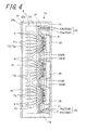
- Fig. 4 is a plan view of the head base 3.
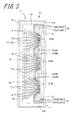
- Fig. 5 is a plan view of the head base 3 in which a later-described first protection film 25, a second protection film 28, a first covering layer 24, the driver ICs 11 and a covering member 29 are not shown.
- the substrate 7 has a rectangular shape, including one main surface, the other main surface arranged on the opposite side of one main surface and a plurality of side surfaces connecting one main surface and the other main surface. An edge 7a of the substrate 7 is formed at a ridgeline portion formed by one main surface and the side surfaces.
- the substrate 7 is made of an electrically insulating material such as alumina ceramics or a semiconductor material such as monocrystalline silicon.
- a thermal storage layer 13 is disposed on an upper surface of the substrate 7 over the entire upper surface of the substrate 7.
- the upper surface of the substrate 7 corresponds to one main surface in the invention.
- the thermal storage layer 13 is made of, for example, glass having low thermal conductivity and is capable of temporarily accumulating part of heat generated in the heat-generating portions 9, therefore, the thermal storage layer 13 functions so as to shorten the time necessary for increasing the temperature of the heat-generating portions 9 to increase thermal response characteristics of the thermal head X1.
- the thermal storage layer 13 is formed by, for example, applying a given glass paste obtained by mixing a suitable organic solvent into glass powder on the upper surface of the substrate 7 by using a well-known screen printing or the like and firing the mixture at a high temperature.
- the glass for forming the thermal storage layer 13 include glass containing SiO 2 , Al 2 O 3 , CaO and BaO, glass containing SiO 2 , Al 3 O 3 and PbO, glass containing SiO 2 , Al 2 O 3 and BaO, and glass containing SiO 2 , B 2 O 3 , PbO, Al 2 O 3 , CaO and MgO.
- a Vickers hardness of these glasses is approximately 500 to 900 HV.
- An electric resistor layer 15 is disposed above the upper surface of the thermal storage layer 13.
- the electric resistor layer 15 is interposed between the thermal storage layer 13 and a later-descried common electrode wiring 17, individual electrode wirings 19, a ground electrode wiring 21 and IC control wirings 23.
- the electric resistor layer 15 has regions having the same shapes as the individual electrode wirings 19, the common electrode wiring 17, the ground electrode wiring 21 and the IC control wirings 23 in a plan view (hereinafter referred to as interposed regions) as well as a plurality of regions exposed from between the common electrode 17 and the individual electrode wirings 19 as shown in Fig. 5 (hereinafter referred to as exposed regions). Note that the interposed regions of the electric resistor layer 15 are hidden by the common electrode wiring 17, the individual electrode wirings 19, the ground electrode wiring 21 and the IC control electrode wirings 23 in Fig. 5 .
- the respective exposed regions of the electric resistor layer 15 form the heat-generating portions 9.
- the plurality of heat-generating portions 9 are arranged in a line on the thermal storage layer 13 as shown in Figs. 2 and 5 .
- the plurality of heat-generating portions 9 are shown in a simple manner for convenience of description in Figs. 1 , 4 and 5 , which are arranged in a density of, for example, 180 to 2400 dpi (dot per inch).
- the exposed regions of the electric resister layer 15 to be the heat-generating portions 9 correspond to electric resistors of the invention.
- the electric resistor layer 15 is made of a material having relatively high electric resistance such as a TaN-based, a TaSiO-based, a TaSiNO-based, a TiSiO-based, a TiSiCO-based or a NbSiO-based material. Accordingly, when a voltage is applied between the later-described common electrode wiring 17 and the individual electrode wirings 19, and the voltage is applied to the heat-generating portions 9, the heat-generating portions 9 generate heat due to Joule heat.
- the common electrode wiring 17, individual electrode wirings 19, the ground electrode wiring 21 and the IC control wirings 23 are disposed on an upper surface of the electric resistor layer 15.
- These common electrode wiring 17, the individual electrode wirings 19, the ground electrode wiring 21 and the IC control wirings 23 are made of a material having conductivity, which is, for example, at least one metal selected from aluminum, gold, silver and copper or an alloy including these metals.
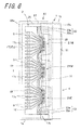
- Fig. 6 is a plan view showing a state where the FPC 5 is connected to the head base 3 in which the later-described first protection film 25, the second protection film 28, the first covering layer 24 and the covering member 29 are not shown.
- the common electrode 17 has a main wiring portion 17a extending along one long side of the substrate 7, two sub-wiring portions 17b respectively extending one and the other short sides of the substrate 7, one end portions of which are connected to the main wiring portion 17a, a plurality of lead portions 17c extending toward the respective heat-generating portions 9 from the main wiring portion 17a. Then, the other end portions of the sub-wiring portions 17b are connected to the FPC 5 as well as tip portions of the lead portions 17c are connected to the heat-generating portions 9 as shown in Fig. 6 . Accordingly, the FPC 5 and the heat-generating portions 9 are electrically connected.
- the individual electrode wirings 19 extend between the respective heat-generating portions 9 and the driver ICs 11 to connect them to each other as shown in Figs. 2 and 6 .
- the individual electrode wirings 19 divide the plurality of heat-generating portions 9 into a plurality of groups, and electrically connect the heat-generating portions 9 in the respective groups to the driver ICs 11 provided so as to correspond to respective groups.
- the main wiring portion 17a of the common electrode wiring 17 is disposed above the thermal storage layer 13 apart from the edge 7a of the substrate 7 as shown in Fig. 6 . That is, the common electrode wiring 17 and the individual electrode wirings 19 are disposed above the thermal storage layer 13 apart from the edge 7a of the substrate 7. In the present embodiment, the common electrode wirings 17 and the individual electrode wirings 19 correspond to electrodes in the invention.
- the ground electrode wiring 21 extends along the arrangement direction of the heat-generating portions 9 in a band shape in the vicinity of the other long side of the substrate 7 as shown in Fig. 5 .
- the FPC 5 and the driver ICs 11 are connected as shown in Figs. 3 and 6 .
- the FPC 5 is connected to end portion regions 21E positioned at one and the other end portions of the ground electrode wiring 21 on both end portion sides as shown in Fig. 6 .
- the FPC 5 is also connected to an intermediate region 21M of the ground electrode wiring 21 positioned between adjacent driver ICs 11 on a center side.
- the driver ICs 11 are arranged so as to correspond to the respective groups of the plurality of heat-generating portions 9 and are connected to one end portions of the individual electrode wirings 19 and the ground electrode wiring 21 as shown in Fig. 6 .
- the drivers IC 11 are configured to control a conducting state of respective heat-generating portions 9, and well-known ones having a plurality of switching devices thereinside can be used, which become conductive when the respective switching devices are in an on-state and become nonconductive when respective switching devices are in an off-state.
- each driver IC 11 as shown in Fig.
- connection terminals 11a connected to the internal switching devices (hereinafter referred to as first connection terminals 11a) are connected to the individual electrode wirings 19, and the other connection terminals 11b connected to the switching devices (hereinafter referred to as second connection terminals 11b) are connected to the ground electrode wiring 21. Accordingly, when respective switching devices of the driver IC 11 are in the on-state, the individual electrode wirings 19 connected to the respective switching devices are electrically connected to the ground electrode wiring 21.
- a plurality of the first connection terminals 11a and the second connection terminals 11b are provided so as to correspond to the respective individual electrode wirings 19, though not shown.
- the plurality of first connection terminals 11a are individually connected to the respective individual electrode wirings 19.
- the plurality of second connection terminals 11b are connected to the ground electrode wiring 21 in common.
- the IC control wirings 23 are for controlling the driver ICs 11, having IC power wirings 23a and IC signal wirings 23b as shown in Fig. 5 .
- the IC power wirings 23a include end-portion power wiring portions 23aE arranged in the vicinity of the right long side of the substrate 7 at both end portions in the longitudinal direction of the substrate 7 and intermediate power wiring portions 23aM arranged between adjacent driver ICs 11.
- the end-portion power wiring portion 23aE is arranged so that one end portion thereof is arranged at an arrangement region of the driver IC 11 and the other end portion thereof is arranged in the vicinity of the right long side of the substrate 7 in a manner of being drawn around the grand electrode wiring 21.
- the end-portion power wiring portion 23aE is arranged so that one end portion thereof is connected to the driver IC 11 and the other end portion thereof is connected to the FPC 5. Accordingly, the driver ICs 11 are electrically connected to the FPC 5.
- the intermediate power wiring portion 23aM extends along the ground electrode wiring 21, one end portion is arranged at an arrangement region of one of adjacent driver ICs 11 and the other end portion is arranged at an arrangement region of the other of adjacent driver ICs 11.
- the intermediate power wiring portion 23aM is arranged so that one end portion thereof is connected to one of adjacent driver ICs 11, the other end portion thereof is connected to the other of adjacent driver ICs 11, and an intermediate portion thereof is connected to the FPC 5 (refer to Fig. 3 ). Accordingly, the driver ICs 11 are electrically connected to the FPC 5.
- the end-portion power wiring portion 23aE and the intermediate power wiring portion 23aM are electrically connected to each other inside the driver IC 11 to which both power wiring portions are connected.
- the adjacent intermediate power wiring portions 23aM are electrically connected to each other inside the driver IC 11 to which both wiring portions are connected.
- the IC power wirings 23a electrically connect between respective driver ICs 11 and the FPC 5 by connecting the IC power wirings 23a to the respective driver ICs 11. Accordingly, electric current is supplied from the FPC 5 to the respective driver ICs 11 through the end-portion power wiring portions 23aE and the intermediate power wiring portions 23aM as described later.
- the IC signal wirings 23b include end-portion signal wiring portions 23bE arranged in the vicinity of the right long side of the substrate 7 at both end portions in the longitudinal direction of the substrate 7 and intermediate signal wiring portions 23bM arranged between adjacent driver ICs 11 as shown in Fig. 5 .
- the end-portion signal wiring portion 23bE is arranged so that one end portion thereof is arranged at the arrangement region of the driver IC 11 and the other end portion thereof is arranged in the vicinity of the right long side of the substrate 7 in a manner of being drawn around the grand electrode wiring 21 in the same manner as the end-portion power wiring portion 23aE.
- the end-portion signal wiring portion 23bE is arranged so that one end portion thereof is connected to the driver IC 11 and the other end portion thereof is connected to the FPC 5.
- the intermediate signal wiring portion 23bM is arranged so that one end portion thereof is arranged at an arrangement region of one of adjacent driver ICs 11 and the other end portion thereof is arranged at an arrangement region of the other of adjacent driver ICs 11 in a manner of being drawn around the intermediate power wiring portion 23aM.
- the intermediate signal wiring portion 23bM is arranged so that one end portion thereof is connected to one of adjacent driver ICs 11 and the other end portion thereof is connected to the other of adjacent driver ICs 11.
- the end-portion signal wiring portion 23bE and the intermediate signal wiring portion 23bM are electrically connected to each other inside the driver IC 11 to which both wiring portions are connected.
- the adjacent intermediate signal wiring portions 23bM are electrically connected to each other inside the driver IC to which both wiring portions are connected.
- the IC signal wirings 23b electrically connect between the respective driver ICs 11 and the FPC 5 by connecting the IC signal wirings 23b to the respective driver ICs 11. Accordingly, a control signal transmitted from the FPC 5 to the driver IC 11 through the end-portion signal wiring portion 23bE is further transmitted to the adjacent driver IC 11 through the intermediate signal wiring portion 23bM as described later.
- the above-described electric resistor layer 15, the common electrode wiring 17, the individual electrode wirings 19, the ground electrode wiring 21 and IC control wirings 23 are formed by, for example, sequentially stacking material layers forming respective components on the thermal storage layer 13 by using, for example, a well-known thin-film forming technique such as sputtering, then, processing a stacked body into a given pattern by using a well-known photolithography technique, an etching technique or the like.
- the first covering layer 24 covering part of the heat-generating portions 9, the common electrode wiring 17 and part of the individual electrode wirings 19 is disposed above the thermal storage layer 13 formed on the upper surface of the substrate 7.
- the first covering layer 24 is disposed so as to cover the approximately left half of the upper surface of the thermal storage layer 13, and the left end of the first covering layer 24 extends to the end of the thermal storage layer 13.
- the first covering layer 24 is formed on the heat-generating portions 9, the common electrode wiring 17 and the individual electrode wirings 19 as well as extends from atop the heat-generating portions 9, the common electrode wiring 17 and the individual electrode wirings 19 as seen from a direction orthogonal to one main surface of the substrate 7 toward atop the thermal storage layer 13 on the edge 7a of the substrate 7.
- the first covering layer 24 extends from atop the main wiring portion 17a of the common electrode wiring 17 further toward atop the thermal storage layer 13 on the edge 7a of the substrate 7, on the thermal storage layer 13.
- the first covering layer 24 is configured to suppress covered portions of the heat-generating portions 9, the common electrode wiring 17 and the individual electrode wirings 19 to be oxidized due to reaction with oxygen or to be corroded due to adhesion of moisture or the like included in the air.
- the first covering layer 24 is made of a material having a high Vickers hardness value than the thermal storage layer 13, which can be made by materials such as SiN, SiC or SiON. These materials can include other elements such as Al.
- a Vickers hardness of SiN is approximately 1600 to 1800 HV
- a Vickers hardness of SiC is approximately 2000 to 2200 HV
- a Vickers hardness of SiON is approximately 1200 to 1400 HV.
- the first covering layer 24 can be formed by using a well-known thin-film forming technique or the like such as sputtering or vapor deposition.
- the first covering layer 24 can be formed by stacking a plurality of material layers.
- a second covering layer 26 may be disposed on the first covering layer 24.
- the second covering layer 26 is preferably made of a material different from the first covering layer 24, for example, can be made of materials such as SiN, SiC or SiON.
- the second covering layer 26 made of a different material is disposed on the first covering layer 24 as described above, the possibility that the heat-generating portions 9, the common electrode wiring 17 and the individual electrode wirings 19 are oxidized can be further reduced.
- the second covering layer 26 is disposed on the first covering layer 24, and an edge 26a of the second covering layer 26 can be disposed on an edge 24a of the first covering layer 24. Accordingly, the possibility that the heat-generating portions 9, the common electrode wiring 17 and the individual electrode wirings 19 are oxidized can be much further reduced.
- the second covering layer 26 preferably has a higher Vickers hardness than the first covering layer 24.
- the first covering layer 24 is made of SiN having the Vickers hardness of approximately 1600 to 1800 HV and the second covering layer 26 is made of SiC having the Vickers hardness of approximately 2000 to 2200 HV, thereby improving abrasion resistance of the second covering layer 26 making contact with a recording medium and obtaining the first covering layer 24 and the second covering layer 26 in which oxidation resistance and abrasion resistance have been improved.
- the second covering layer 26 is made of a material having a lower Vickers hardness than that of the first covering layer 24.
- the first covering layer 24 is made of SiN having the Vickers hardness of approximately 1600 to 1800 HV and the second covering layer 26 is made of SiON having the Vickers hardness of approximately 1200 to 1400 HV or SiO 2 having a Vickers hardness of 600 to 800 HV, thereby alleviating stress by the second covering layer 26 and reducing the possibility that a chip or a crack occurs in the first covering layer 24 and the second covering layer 26 even when large stress is generated in the first covering layer 24 and the second covering layer 26 at the time of separating the thermal head X1 from a mother board, which will be described later in detail.
- the second covering layer 26 is made of SiO 2 having the Vickers hardness of 600 to 800 HV which is softer than the first covering layer 24, adhesiveness with respect to the first protection film 25 can be increased as well as stress generating at the time of separating the substrate is alleviated to thereby obtain the thermal head X1 in which the possibility that a chip or a crack occurs is reduced in the case where the first covering layer 24 is made of SiN having the Vickers hardness of 1600 to 1800 HV. It is not always necessary that the edge of the second covering layer 26 is disposed above the edge 7a of the substrate 7, and it is preferable that the edge of the second covering layer 26 is disposed between the edge 7a of the substrate 7 and the edge 25a of the first protection film 25. Accordingly, the possibility that a crack occurs in the second covering layer 26 can be reduced.
- the first protection film 25 is disposed on or above the first covering layer 24.
- the first protection film 25 is disposed so as to cover the first covering layer 24 except a region in the vicinity of the edge 24a on the left side of the first covering layer 24 in the shown example. That is, the first covering layer 24 is not disposed above the edge 7a of the substrate 7.
- the first protection film 25 is disposed on or above the first covering layer 24, and the edge 25a of the first protection film 25 is disposed apart from the edge 7a of the substrate 7.
- the first protection film 25 is disposed on or above the first covering layer 24 over the heat-generating portions 9, the common electrode wiring 17 and the individual electrode wirings 19 as seen from a direction orthogonal to the upper surface of the substrate 7.
- the edge 25a of the first protection film 25 extends on the first covering layer 24 so as to be positioned between the heat-generating portions 9, the common electrode wiring 17 and the individual electrode wirings 19, and the edge 7a of the substrate 7.
- the first protection film 25 extends on the first covering layer 24 so that the edge 25a of the first protection film 25 is positioned between the main wiring portion 17a of the common electric wiring 17 and the edge 7a of the substrate 7.
- the first protection film 25 corresponds to the protection film in the invention.
- the possibility that a crack occurs in the first protection film 25 can be reduced. Accordingly, the heat-generating portions 9, the common electrode wiring 17 and the individual electrode wirings 19 can be sealed with the first protection film 25 even when the crack occurs in the thermal storage layer 13. As a result, the corrosion and deterioration of the heat-generating portions 9, the common electrode wiring 17 and the individual electrode wirings 19 can be reduced.
- the thermal storage layers, electrode wirings, the heat-generating resistors, the protection films or the like to be a plurality of thermal heads are formed at a time on a large mother board from which a plurality of substrates each for forming one thermal head can be taken.
- the thermal storage layer included in the respective thermal heads is formed so as to extend over a plurality of substrates forming a plurality of thermal heads. Accordingly, the thermal storage layer exists on dividing lines of the mother board, namely, on edges of substrates in the respective thermal heads. In such case, a crack may occur in the thermal storage layer arranged on edges of divided substrates when the mother board is divided. Since the crack extends due to thermal response at the time of driving the thermal head, there is a possibility that corrosion or deterioration of the heat-generating resistors 9 occurs when a crack connecting through an upper surface and a lower surface of the thermal storage layer 13 occurs.
- the first covering layer 24 extends from atop the main wiring portion 17a of the common electric wiring 17 toward atop the thermal storage layer 13 on the edge 7a of the substrate 7 as seen from the direction orthogonal to the upper surface of the substrate 7, therefore, the thermal storage layer 13 on the edge 7a of the substrate 7 to be a dividing line is covered by the first covering layer 24, for example, even when the edge 7a of the substrate 7 is the dividing line of the mother board as in the related art example. Accordingly, it is possible to reduce the occurrence of a chip or a crack on the thermal storage layer 13 made of glass on the edge 7a of the divided substrate 7 in the case where the mother board is divided as in the related art example.
- the occurrence of a crack in the thermal storage layer 13 can be reduced by the first covering layer 24 provided for suppressing oxidation of the heat-generating portions 9, the common electrode wiring 17 and the individual electrode wirings 19, therefore, the structure of the thermal head X1 can be simplified.
- the first protection film 25 is configured to protect the heat-generating portions 9, the common electrode wiring 17 and the individual electrode wirings 19 from the abrasion due to the contact to the recording medium to be printed.
- the first protection film 25 can be made of materials such as glass containing SiO 2 , Bi 2 O 3 and ZnO, glass containing SiO 2 , B 2 O 3 and PbO, glass containing SiO 2 , PbO and ZnO, glass containing SiO 2 , B 2 O 3 and RO and glass containing SiO 2 , ZnO and RO or materials such as SiN, SiC or SiON.
- the Vickers hardness will be 300 to 600 HV.
- the first protection film 25 can also be formed by using, for example, a thick-film forming technique such as screen printing, a well-known thin-film forming technique such as sputtering or deposition.
- a film defect can be filled by the first protection film 25 even when the film defect occurs in a portion of the first covering layer 24 covered by the first protection film 25.
- the first protection film 25 may be formed by stacking a plurality of material layers.
- the thermal head X1 when the thermal storage layer 13 and the first covering layer 24 disposed above the edge 7a of the substrate 7 provided at corner portions which are liable to collide with exterior components unexpectedly touch a casing of a thermal printer or the like and thus a crack occurs in the thermal storage layer 13 and the first covering layer 24, for example, in the case where the thermal head X1 is assembled to a body of the thermal printer, the possibility of crack extension can be reduced as the first protection film 25 is not disposed above the edge 7a of the substrate.
- the first protection 25 is not disposed above the edge 7a of the substrate 7 to be the dividing line of the mother board.
- the possibility that a crack occurs in the first protection film 25 can be reduced even when the substrate 7 is divided at the edge 7a, because the first protection film 25 is disposed apart from the edge 7a of the substrate 7 which is the dividing line. Accordingly, it is possible to reduce the extension of the crack occurring in the thermal storage layer 13 at the same time as the crack occurring in the first protection film 25 extends.
- the first protection film 25 is disposed on or above the first covering layer 24 so that the edge 25a of the first protection film 25 is positioned between the main wiring portion 17a of the common electrode wiring 17 and the edge 7a of the substrate 7 as seen from the direction orthogonal to the upper surface of the substrate 7.
- the first protection film 25 is disposed apart from the edge 7a of the substrate 7 to be the dividing line at the time of dividing the mother board as in the related art example, it is possible to reduce the crack extension by the first protection film 25 disposed apart from the edge 7a of the substrate 7 even when the crack occurs in the glass-made thermal storage layer 13 disposed on the edge 7a of the substrate 7 as well as in the first covering layer 24 when the mother board is divided.
- the mother board can be divided while checking the dividing lines. Accordingly, the dividing accuracy in a dividing process of the substrate can be improved.
- the first protection film 25 has a lower Vickers hardness than that of the thermal storage layer 13.
- the first protection film 25 can be made of Pb-based glass or Bi-based glass. Since the first protection film 25 has a lower Vickers hardness than that of the thermal storage layer 13 as described above, the extension of a chip or a crack can be suppressed by the soft first protection film 25 even when the crack occurs in the thermal storage layer 13 and the first covering layer 24.
- the edge 25a of the first protection film 25 is vertically provided has been shown in the thermal head X1, the invention is not limited to this. It is also preferable that, for example, the edge 25a has a tapered shape gradually sloping toward the edge 7a of the substrate 7.
- the second protection film 28 partially covering the common electrode wiring 17, the individual electrode wirings 19, the IC control wirings 23 and the ground electrode wiring 21, is disposed above the thermal storage layer 13 formed on the upper surface of the substrate 7.
- the second protection film 28 is disposed so as to partially cover a region of approximately the right half of the upper surface of the thermal storage layer 13.
- the second protection film 28 is configured to protect the covered common electrode wiring 17, the individual electrode wirings 19, the IC control wirings 23 and the ground electrode wiring 21 from oxidation due to contact with the air and corrosion due to adhesion of moisture or the like included in the air.
- the second protection film 28 is disposed so as to overlap with an end portion of the first protection film 25 for securing the protection of the common electrode wiring 17, the individual electrode wirings 19 and the IC control wirings 23.
- the second protection film 28 can be made of, for example, resin materials such as epoxy resin and polyimide resin. Additionally, the second protection film 28 can be formed by using the thick-film forming technique such as screen printing.
- openings for exposing end portions of the individual electrode wirings 19 connecting the driver ICs 11, an second intermediate region 21N and a third intermediate region 21L of the ground electrode wiring 21 and end portions of the IC control wirings 23 are formed in the second protection film 28, and these wirings are connected to the driver ICs 11 through the openings.
- the driver ICs 11 are sealed by being covered with a covering member 29 made of resin such as epoxy resin or silicone resin for protecting the driver ICs 11 themselves and connecting portions between the driver ICs 11 and these wirings in a state of being connected to the individual electrode wirings 19, the ground electrode wiring 21 and the IC control wirings 23.
- the FPC 5 is connected to the common electrode wiring 17, the ground electrode wiring 21 and IC control wirings 23 as described above.
- a well-known board in which a plurality of printed wirings are arranged inside an insulating resin layer can be used, in which respective printed wirings are electrically connected to an external power supply device, a controller and the like, which are not shown, through a connector 31 (refer to Figs. 1 and 6 ).
- the respective printed wirings disposed thereinside are connected to end portions of the two sub-wiring portions 17b of the common electric wiring 17, end portions of the ground electrode wiring 21 and end portions of the IC control wirings 23 to thereby connect between these wirings 17, 21 and 23 and the connector 31 by solder bumps 33 (refer to Fig. 3 ).
- the connector 31 is electrically connected to the external power supply device, the controller and the like (not shown)
- the common electrode wiring 17 is connected to a positive-side terminal of the power supply device held in a positive potential of 20 to 24 V and the individual electrode wirings 19 are electrically connected to a negative-side terminal of the power supply device held in a ground potential of 0 to 1 V. Accordingly, electric current is supplied to the heat-generating portions 9 when the switching devices of the driver ICs 11 are in the on-state, and the heat-generating portions 9 generate heat.
- the IC power wirings 23a of the IC control wirings 23 are connected to the positive-side terminal of the power supply device held in the positive potential in the same manner as the common electrode wiring 17. Accordingly, electric current for operating the driver ICs 11 is supplied to the driver ICs 11 by the difference of potentials in the IC power wirings 23a to which the driver ICs 11 are connected and the ground electrode wiring 21.
- the IC signal wirings 23b of the IC control wirings 23 are connected to the controller performing control of the driver ICs 11.
- a control signal from the controller is transmitted to the driver IC 11 through the end-portion signal wiring portion 23bE, and the control signal transmitted to the driver IC 11 is further transmitted to the adjacent driver IC through the intermediate signal wiring portion 23bM.
- the on/off states of the switching devices inside the drivers IC 11 are controlled by the control signal, thereby allowing the heat-generating portions 9 to generate heat selectively.
- the manufacturing method of the thermal head X1 includes a process of forming the thermal storage layer 13 over the entire surface of the mother board, a process of forming the electric resistor layer 15 over the entire surface of the thermal storage layer 13, and a process of forming a conductive layer (not shown) to be various types of electrodes such as the common electrode wiring 17 over the entire surface of the electric resistor layer 15.
- the manufacturing method further includes a process of patterning the electric resistor layer 15 and the conductive layer, a process of forming the first covering layer on the conductive layer other than a portion to be connected to the FPC 5, and a process of forming the first protection film 25 in a given position and firing the film.
- the first protection film 25 is not disposed on the dividing lines of the mother board.
- the second protection film 28 is formed in a given position and the mother board is divided along the dividing lines, thereby fabricating the thermal head X1.
- the process of forming respective component members, the process of performing patterning and the process of dividing can be performed by using any methods generally known in the thin-film or thick-film forming techniques.
- the given position where the first protection film 25 is formed differs according to the number of thermal heads X1 to be divided from the mother board.
- a case where two thermal heads X1 are divided from the mother board will be described as an example.
- various electrode wirings such as the common electrode wiring are patterned so as to be mirror images to each other with respect to the central line of the mother board. That is, various members are formed by performing patterning so that the dividing line of the substrates 7 will be the central line of the mother board. Then, the first protection film 25 is formed between the heat-generating portions 9 and the dividing line of the substrates 7. Accordingly, the first protection films 25 which are parallel to each other may be formed to indicate the dividing line of the substrates 7.
- the thermal storage layer 13 and the first covering layer 24 are disposed and the first protection film 25 is not disposed on the dividing line of the substrate 7, and therefore the first covering layer 24 can reduce the possibility that a crack occurring in the thermal storage layer 13 extends even when the substrate 7 is divided at the dividing line. Moreover, as the first protection film 25 is not disposed on the dividing line of the substrate 7, the possibility that a crack occurs in the first protection film 25 can be suppressed.
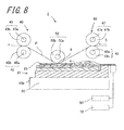
- Fig. 8 is a schematic structure view of a thermal printer Z according to the present embodiment.
- the thermal printer Z includes the above-described thermal head X1, a conveyance mechanism 40, a platen roller 50, a power supply device 60 and a controller 70.
- the thermal head X1 is attached to an attachment surface 80a of an attachment member 80 provided in a casing (not shown) of the thermal printer Z.
- the thermal head X1 is attached to the attachment member 80 so that the arrangement direction of the heat-generating elements 9 is along a direction (a main scanning direction) orthogonal to a conveying direction S of a later-described recording medium P, namely, a direction orthogonal to a plane of paper of Fig. 8 .
- the conveyance mechanism 40 is configured to convey the recording medium P such as heat-sensitive paper or receiver paper on which ink is transferred in a direction of an arrow S in Fig. 8 to be conveyed on a plurality of heat-generating elements 9 of the thermal head X1, having conveyance rollers 43, 45, 47 and 49.
- the conveyance rollers 43, 45, 47 and 49 can be formed by, for example, coating cylindrical shafts 43a, 45a, 47a and 49a made of a metal such as stainless steel with elastic members 43b, 45b, 47b and 49b made of butadiene rubber or the like.
- the platen roller 50 is configured to press the recording medium P on the heat-generating elements 9 of the thermal head X1, which is arranged so as to extend along a direction orthogonal to the conveying direction S of the recording medium P, both end portions of which are supported so as to be rotated in a state of pressing the recording medium P on the heat-generating elements 9.
- the platen roller 50 can be formed by, for example, coating a cylindrical shaft 50a made of a metal such as stainless steel with an elastic member 50b made of butadiene rubber or the like.
- the power supply device 60 is configured to apply a voltage for allowing the heat-generating elements 9 of the thermal head X1 to generate heat and a voltage for operating the driver ICs 11 as described above.
- the controller 70 is configured to supply a control signal controlling the operation of the driver ICs 11 to the driver ICs 11 for allowing the heat-generating elements 9 of the thermal head X1 to generate heat selectively as described above.
- the thermal printer Z can perform given printing on the recording medium P by allowing the heat-generating elements 9 to generate heat selectively by the power supply device 60 and the controller 70 while pressing the recording medium on the heat-generating elements 9 of the thermal head X1 by the platen roller 50 and conveying the recording medium P on the heat-generating elements 9 by the conveyance mechanism 40 as shown in Fig. 8 .
- the recording medium P is the receiver paper or the like
- the printing on the recording medium P can be performed by thermally transferring ink of the ink film (not shown) conveyed together with the receiving medium P on the recording medium P.
- FIG. 9 A thermal head X2 according to a second embodiment will be described with reference to Figs. 9 and 10.
- Figs. 9 and 10 are views respectively corresponding to Figs. 2 and 3 , and a plan view of the thermal head X2 is not shown.
- the thermal head X2 has the second protection film 28 as a resin layer extending from the edge 7a of the substrate 7 onto the first protection film 25. Other portions are the same as those of the thermal head X1, and description thereof is omitted.
- one end portion 28b thereof is disposed on the first protection film 25, and the other end portion 28a thereof is disposed above the edge 7a of the substrate 7. Then, a convex portion 30 higher than other portions is disposed on the edge 7a side of the substrate 7. As shown in Figs. 9 and 10 , the convex portion 30 is formed in the other end portion 28a of the second protection film 28.
- the convex portion 30 of the second protection film 28 is located at a higher position than other portions of the second protection film 28. Accordingly, the recording medium, particularly, an ink ribbon having passed on the heat-generating portions 9 is pushed toward a separating direction due to the presence of the convex portion 30 of the second protection film 28. As a result, the separation between the thermal head X2 and the ink ribbon can be smoothly performed. Accordingly, the thermal head X2 capable of performing printing at high speed can be obtained.
- the second protection film 28 is made of soft resin and is disposed above the edge 7a of the substrate 7, the second protection film 28 disposed on the edge 25a of the first protection film 25 can alleviate stress even when the stress generated by the crack extension occurring in the thermal storage layer 13 occurs in the first protection film 25. Accordingly, the possibility that the first protection film 25 separates from the first covering layer 24 can be reduced.
- the convex portion 30 of the second protection film 28 is disposed above the edge 7a of the substrate 7. Accordingly, the separation between the thermal head X2 and the ink ribbon can be performed more smoothly.
- the first protection film 25 is formed above the mother board in the same method as the thermal head X1. After that, as shown in Figs. 9 and 10 , the second protection film 28 is formed on the dividing line and on the side connected to the FPC 5.
- a method of forming the convex portion 30 of the second protection film 28 for example, it is possible to form the convex portion 30 by coating the other end portion 28a with a resin material plural times as well as by coating the second protection film 28 from the other end portion 28a side by using a resin having high viscosity.
- the common electrode wiring 17 and the individual electrode wirings 19 are formed on the electric resistor layer 15 in the thermal head X1 according to the above embodiment as shown in Fig. 2 , the invention is not limited to this as long as both the common electrode wiring 17 and the individual electrode wirings 19 are connected to the electric resistors to be the heat-generating portions.
- the common electrode wiring 17 and the individual electrode wirings 19 are formed on the thermal storage layer 13, then, the electric resistor layer 15 is formed on the thermal storage layer 13 on which the common electrode wiring 17 and the individual electrode wirings 19 are formed as shown Fig. 11 .
- regions on the electrode resistor layer 15 positioned between the common electrode wiring 17 and the individual electrode wirings 19 will be electric resistors in the invention, and the regions form the heat-generating portions 9.
- the common electrode wiring 17 and the individual electrode wirings 19 are formed on the thermal storage layer 13, and the electric resistor layer 15 is formed only in regions between the common electrode wiring 17 and the individual electrode wirings 19 as shown in Fig. 12 .
- the electric resistor layer 15 will be the electric resistors in the invention, and the electric resistor layer 15 form the heat-generating portions 9.
Landscapes
- Physics & Mathematics (AREA)
- Geometry (AREA)
- Electronic Switches (AREA)
Abstract
Description
- The present invention relates to a thermal head and a thermal printer including the same.
- Various types of thermal heads have been heretofore proposed as printing devices for a facsimile, a video printer or the like. For example, a thermal head described in
Patent Literature 1 includes a substrate, a thermal storage layer disposed on one main surface of the substrate so as to extend to an edge of the substrate, the thermal storage layer being made of glass, electrodes disposed above the thermal storage layer apart from the edge of the substrate, heat-generating resistors connected to the electrodes, a covering layer disposed on the electrodes and the heat-generating resistor and a protection film disposed on the covering layer (for example, refer to Patent Literature 1). -
- Patent Literature 1: Japanese Unexamined Patent Publication
JP-A 2009-131994 - In the above thermal head, there is a case where a crack occurs in the thermal storage layer made of glass, and there is a possibility that the crack occurring in the thermal storage layer further extends and penetrates upper and lower surfaces of the thermal storage layer when the thermal head is driven. Accordingly, a chip may occur in the thermal storage layer and the electrodes and the heat-generating resistor may deteriorate.
- A thermal head according to an embodiment of the invention includes a substrate; a thermal storage layer disposed on one main surface of the substrate so as to extend to an edge of the substrate, the thermal storage layer being formed of glass; electrodes disposed on or above the thermal storage layer apart from the edge of the substrate; heat-generating resistors disposed above the thermal storage layer apart from the edge of the substrate, the heat-generating resistors being connected to the electrodes; a first covering layer disposed on or above the electrodes and the heat-generating resistors; and a protection film disposed on or above the first covering layer, the first covering layer extending from atop the electrodes and the heat-generating resistors toward atop the thermal storage layer on the edge of the substrate, the protection film being disposed on or above the first covering layer disposed on or above the electrodes and the heat-generating resistors and an edge of the protection film being not disposed above the edge of the substrate.
- A thermal printer according to an embodiment of the invention includes the thermal head mentioned above; a conveyance mechanism that conveys a recording medium on a plurality of heat-generating portions; and a platen roller that presses the recording medium on the plurality of heat-generating portions.
- According to the invention, possibility of crack extension can be reduced even if any crack occurs in the thermal storage layer.
-
-
Fig. 1 is a plan view showing a thermal head according to one embodiment of the invention; -
Fig. 2 is a cross-sectional view of the thermal head taken along the line I-I ofFig. 1 ; -
Fig. 3 is a cross-sectional view of the thermal head taken along the line II-II ofFig. 1 ; -
Fig. 4 is a plan view of a head base in the thermal head ofFig. 1 ; -
Fig. 5 is a plan view of the head base ofFig. 4 in which a first protection film, a second protection film, a first covering layer, driver ICs and a covering member are not shown; -
Fig. 6 is a plan view showing a state where an FPC is connected to the head base in which the first protection film, the second protection film, the first covering layer and the covering member are not shown; -
Fig. 7 is a partially-enlarged view showing a modified example of the thermal head according to one embodiment of the invention in a cross section of the thermal head shown inFig. 2 ; -
Fig. 8 is a schematic view showing an outline of a thermal printer according to one embodiment of the invention; -
Fig. 9 is a cross-sectional view in a thermal head according to another embodiment of the invention, which corresponds toFig. 2 ; -
Fig. 10 is a cross-sectional view in a thermal head according to another embodiment of the invention, which corresponds toFig. 3 ; -
Fig. 11 is a partially enlarged view showing a modified example of a thermal head according to another embodiment of the invention in the cross section shown inFig. 2 ; and -
Fig. 12 is a partially-enlarged view showing a modified example of a thermal head according to another embodiment of the invention in the cross section shown inFig. 2 . - Hereinafter, a thermal head according to one embodiment of the invention will be described with reference to the drawings. As shown in
Figs. 1 to 3 , a thermal head X1 of the present embodiment includes aheatsink 1, ahead base 3 arranged on theheatsink 1 and a flexible printed circuit board 5 (hereinafter referred to as an FPC 5) connected to thehead base 3. - The
heatsink 1 is made of a metal material such as copper or aluminum, including abed plate portion 1a having a rectangular shape in a plan view and a protrudingportion 1b extending along one long side of thebed plate portion 1a. As shown inFig. 2 , thehead base 3 is bonded to an upper surface of thebed plate portion 1a other than the protrudingportion 1b by a double-faced tape, adhesives or the like (not shown). The FPC 5 is bonded to the protrudingportion 1b by the double-faced tape, adhesives or the like (not shown). Moreover, theheatsink 1 has a function of radiating part of heat not contributing to printing in heat generated at heat-generatingportions 9 of thehead base 3 as described later. - As shown in
Figs. 1 to 5 , thehead base 3 includes asubstrate 7 having a rectangular shape in a plan view, a plurality of heat-generatingportions 9 disposed above thesubstrate 7 and arranged along a longitudinal direction of thesubstrate 7 and a plurality ofdriver ICs 11 arranged side by side on thesubstrate 7 along the arrangement direction of the heat-generatingportions 9.Fig. 4 is a plan view of thehead base 3.Fig. 5 is a plan view of thehead base 3 in which a later-describedfirst protection film 25, asecond protection film 28, a first coveringlayer 24, thedriver ICs 11 and a coveringmember 29 are not shown. - The
substrate 7 has a rectangular shape, including one main surface, the other main surface arranged on the opposite side of one main surface and a plurality of side surfaces connecting one main surface and the other main surface. Anedge 7a of thesubstrate 7 is formed at a ridgeline portion formed by one main surface and the side surfaces. Thesubstrate 7 is made of an electrically insulating material such as alumina ceramics or a semiconductor material such as monocrystalline silicon. - As shown in
Figs. 2, 3 and5 , athermal storage layer 13 is disposed on an upper surface of thesubstrate 7 over the entire upper surface of thesubstrate 7. In the present embodiment, the upper surface of thesubstrate 7 corresponds to one main surface in the invention. Thethermal storage layer 13 is made of, for example, glass having low thermal conductivity and is capable of temporarily accumulating part of heat generated in the heat-generatingportions 9, therefore, thethermal storage layer 13 functions so as to shorten the time necessary for increasing the temperature of the heat-generatingportions 9 to increase thermal response characteristics of the thermal head X1. Thethermal storage layer 13 is formed by, for example, applying a given glass paste obtained by mixing a suitable organic solvent into glass powder on the upper surface of thesubstrate 7 by using a well-known screen printing or the like and firing the mixture at a high temperature. Examples of the glass for forming thethermal storage layer 13 include glass containing SiO2, Al2O3, CaO and BaO, glass containing SiO2, Al3O3 and PbO, glass containing SiO2, Al2O3 and BaO, and glass containing SiO2, B2O3, PbO, Al2O3, CaO and MgO. A Vickers hardness of these glasses is approximately 500 to 900 HV. - An
electric resistor layer 15 is disposed above the upper surface of thethermal storage layer 13. Theelectric resistor layer 15 is interposed between thethermal storage layer 13 and a later-descriedcommon electrode wiring 17,individual electrode wirings 19, aground electrode wiring 21 andIC control wirings 23. Theelectric resistor layer 15 has regions having the same shapes as theindividual electrode wirings 19, thecommon electrode wiring 17, theground electrode wiring 21 and theIC control wirings 23 in a plan view (hereinafter referred to as interposed regions) as well as a plurality of regions exposed from between thecommon electrode 17 and theindividual electrode wirings 19 as shown inFig. 5 (hereinafter referred to as exposed regions). Note that the interposed regions of theelectric resistor layer 15 are hidden by thecommon electrode wiring 17, theindividual electrode wirings 19, theground electrode wiring 21 and the ICcontrol electrode wirings 23 inFig. 5 . - The respective exposed regions of the
electric resistor layer 15 form the heat-generatingportions 9. Then, the plurality of heat-generatingportions 9 are arranged in a line on thethermal storage layer 13 as shown inFigs. 2 and5 . The plurality of heat-generatingportions 9 are shown in a simple manner for convenience of description inFigs. 1 ,4 and5 , which are arranged in a density of, for example, 180 to 2400 dpi (dot per inch). In the present embodiment, the exposed regions of theelectric resister layer 15 to be the heat-generatingportions 9 correspond to electric resistors of the invention. - The
electric resistor layer 15 is made of a material having relatively high electric resistance such as a TaN-based, a TaSiO-based, a TaSiNO-based, a TiSiO-based, a TiSiCO-based or a NbSiO-based material. Accordingly, when a voltage is applied between the later-describedcommon electrode wiring 17 and theindividual electrode wirings 19, and the voltage is applied to the heat-generatingportions 9, the heat-generatingportions 9 generate heat due to Joule heat. - As shown in
Figs. 1 to 6 , thecommon electrode wiring 17,individual electrode wirings 19, theground electrode wiring 21 and theIC control wirings 23 are disposed on an upper surface of theelectric resistor layer 15. Thesecommon electrode wiring 17, theindividual electrode wirings 19, theground electrode wiring 21 and theIC control wirings 23 are made of a material having conductivity, which is, for example, at least one metal selected from aluminum, gold, silver and copper or an alloy including these metals.Fig. 6 is a plan view showing a state where the FPC 5 is connected to thehead base 3 in which the later-describedfirst protection film 25, thesecond protection film 28, the first coveringlayer 24 and the coveringmember 29 are not shown. - As shown in
Fig. 5 , thecommon electrode 17 has amain wiring portion 17a extending along one long side of thesubstrate 7, twosub-wiring portions 17b respectively extending one and the other short sides of thesubstrate 7, one end portions of which are connected to themain wiring portion 17a, a plurality oflead portions 17c extending toward the respective heat-generatingportions 9 from themain wiring portion 17a. Then, the other end portions of thesub-wiring portions 17b are connected to the FPC 5 as well as tip portions of thelead portions 17c are connected to the heat-generatingportions 9 as shown inFig. 6 . Accordingly, the FPC 5 and the heat-generatingportions 9 are electrically connected. - The
individual electrode wirings 19 extend between the respective heat-generatingportions 9 and thedriver ICs 11 to connect them to each other as shown inFigs. 2 and6 . In more detail, theindividual electrode wirings 19 divide the plurality of heat-generatingportions 9 into a plurality of groups, and electrically connect the heat-generatingportions 9 in the respective groups to thedriver ICs 11 provided so as to correspond to respective groups. - The
main wiring portion 17a of thecommon electrode wiring 17 is disposed above thethermal storage layer 13 apart from theedge 7a of thesubstrate 7 as shown inFig. 6 . That is, thecommon electrode wiring 17 and theindividual electrode wirings 19 are disposed above thethermal storage layer 13 apart from theedge 7a of thesubstrate 7. In the present embodiment, thecommon electrode wirings 17 and theindividual electrode wirings 19 correspond to electrodes in the invention. - The
ground electrode wiring 21 extends along the arrangement direction of the heat-generatingportions 9 in a band shape in the vicinity of the other long side of thesubstrate 7 as shown inFig. 5 . On theground electrode wiring 21, theFPC 5 and thedriver ICs 11 are connected as shown inFigs. 3 and6 . In more detail, theFPC 5 is connected to endportion regions 21E positioned at one and the other end portions of theground electrode wiring 21 on both end portion sides as shown inFig. 6 . TheFPC 5 is also connected to anintermediate region 21M of theground electrode wiring 21 positioned betweenadjacent driver ICs 11 on a center side. - The
driver ICs 11 are arranged so as to correspond to the respective groups of the plurality of heat-generatingportions 9 and are connected to one end portions of theindividual electrode wirings 19 and theground electrode wiring 21 as shown inFig. 6 . Thedrivers IC 11 are configured to control a conducting state of respective heat-generatingportions 9, and well-known ones having a plurality of switching devices thereinside can be used, which become conductive when the respective switching devices are in an on-state and become nonconductive when respective switching devices are in an off-state. In eachdriver IC 11, as shown inFig. 2 , oneconnection terminals 11a connected to the internal switching devices (not shown) (hereinafter referred to asfirst connection terminals 11a) are connected to theindividual electrode wirings 19, and theother connection terminals 11b connected to the switching devices (hereinafter referred to assecond connection terminals 11b) are connected to theground electrode wiring 21. Accordingly, when respective switching devices of thedriver IC 11 are in the on-state, theindividual electrode wirings 19 connected to the respective switching devices are electrically connected to theground electrode wiring 21. - A plurality of the
first connection terminals 11a and thesecond connection terminals 11b are provided so as to correspond to the respectiveindividual electrode wirings 19, though not shown. The plurality offirst connection terminals 11a are individually connected to the respectiveindividual electrode wirings 19. The plurality ofsecond connection terminals 11b are connected to theground electrode wiring 21 in common. - The
IC control wirings 23 are for controlling thedriver ICs 11, havingIC power wirings 23a andIC signal wirings 23b as shown inFig. 5 . TheIC power wirings 23a include end-portion power wiring portions 23aE arranged in the vicinity of the right long side of thesubstrate 7 at both end portions in the longitudinal direction of thesubstrate 7 and intermediate power wiring portions 23aM arranged betweenadjacent driver ICs 11. - As shown in
Fig. 5 , the end-portion power wiring portion 23aE is arranged so that one end portion thereof is arranged at an arrangement region of thedriver IC 11 and the other end portion thereof is arranged in the vicinity of the right long side of thesubstrate 7 in a manner of being drawn around thegrand electrode wiring 21. The end-portion power wiring portion 23aE is arranged so that one end portion thereof is connected to thedriver IC 11 and the other end portion thereof is connected to theFPC 5. Accordingly, thedriver ICs 11 are electrically connected to theFPC 5. - As shown in
Fig. 5 , the intermediate power wiring portion 23aM extends along theground electrode wiring 21, one end portion is arranged at an arrangement region of one ofadjacent driver ICs 11 and the other end portion is arranged at an arrangement region of the other ofadjacent driver ICs 11. The intermediate power wiring portion 23aM is arranged so that one end portion thereof is connected to one ofadjacent driver ICs 11, the other end portion thereof is connected to the other ofadjacent driver ICs 11, and an intermediate portion thereof is connected to the FPC 5 (refer toFig. 3 ). Accordingly, thedriver ICs 11 are electrically connected to theFPC 5. - The end-portion power wiring portion 23aE and the intermediate power wiring portion 23aM are electrically connected to each other inside the
driver IC 11 to which both power wiring portions are connected. The adjacent intermediate power wiring portions 23aM are electrically connected to each other inside thedriver IC 11 to which both wiring portions are connected. - As described above, the
IC power wirings 23a electrically connect betweenrespective driver ICs 11 and theFPC 5 by connecting theIC power wirings 23a to therespective driver ICs 11. Accordingly, electric current is supplied from theFPC 5 to therespective driver ICs 11 through the end-portion power wiring portions 23aE and the intermediate power wiring portions 23aM as described later. - The
IC signal wirings 23b include end-portion signal wiring portions 23bE arranged in the vicinity of the right long side of thesubstrate 7 at both end portions in the longitudinal direction of thesubstrate 7 and intermediate signal wiring portions 23bM arranged betweenadjacent driver ICs 11 as shown inFig. 5 . - As shown in
Fig. 5 , the end-portion signal wiring portion 23bE is arranged so that one end portion thereof is arranged at the arrangement region of thedriver IC 11 and the other end portion thereof is arranged in the vicinity of the right long side of thesubstrate 7 in a manner of being drawn around thegrand electrode wiring 21 in the same manner as the end-portion power wiring portion 23aE. The end-portion signal wiring portion 23bE is arranged so that one end portion thereof is connected to thedriver IC 11 and the other end portion thereof is connected to theFPC 5. - The intermediate signal wiring portion 23bM is arranged so that one end portion thereof is arranged at an arrangement region of one of
adjacent driver ICs 11 and the other end portion thereof is arranged at an arrangement region of the other ofadjacent driver ICs 11 in a manner of being drawn around the intermediate power wiring portion 23aM. The intermediate signal wiring portion 23bM is arranged so that one end portion thereof is connected to one ofadjacent driver ICs 11 and the other end portion thereof is connected to the other ofadjacent driver ICs 11. - The end-portion signal wiring portion 23bE and the intermediate signal wiring portion 23bM are electrically connected to each other inside the
driver IC 11 to which both wiring portions are connected. The adjacent intermediate signal wiring portions 23bM are electrically connected to each other inside the driver IC to which both wiring portions are connected. - As described above, the
IC signal wirings 23b electrically connect between therespective driver ICs 11 and theFPC 5 by connecting theIC signal wirings 23b to therespective driver ICs 11. Accordingly, a control signal transmitted from theFPC 5 to thedriver IC 11 through the end-portion signal wiring portion 23bE is further transmitted to theadjacent driver IC 11 through the intermediate signal wiring portion 23bM as described later. - The above-described
electric resistor layer 15, thecommon electrode wiring 17, theindividual electrode wirings 19, theground electrode wiring 21 andIC control wirings 23 are formed by, for example, sequentially stacking material layers forming respective components on thethermal storage layer 13 by using, for example, a well-known thin-film forming technique such as sputtering, then, processing a stacked body into a given pattern by using a well-known photolithography technique, an etching technique or the like. - As shown in
Figs. 2 and 3 , thefirst covering layer 24 covering part of the heat-generatingportions 9, thecommon electrode wiring 17 and part of theindividual electrode wirings 19 is disposed above thethermal storage layer 13 formed on the upper surface of thesubstrate 7. In the shown example, thefirst covering layer 24 is disposed so as to cover the approximately left half of the upper surface of thethermal storage layer 13, and the left end of thefirst covering layer 24 extends to the end of thethermal storage layer 13. Thefirst covering layer 24 is formed on the heat-generatingportions 9, thecommon electrode wiring 17 and the individual electrode wirings 19 as well as extends from atop the heat-generatingportions 9, thecommon electrode wiring 17 and the individual electrode wirings 19 as seen from a direction orthogonal to one main surface of thesubstrate 7 toward atop thethermal storage layer 13 on theedge 7a of thesubstrate 7. In more detail, thefirst covering layer 24 extends from atop themain wiring portion 17a of thecommon electrode wiring 17 further toward atop thethermal storage layer 13 on theedge 7a of thesubstrate 7, on thethermal storage layer 13. - The
first covering layer 24 is configured to suppress covered portions of the heat-generatingportions 9, thecommon electrode wiring 17 and the individual electrode wirings 19 to be oxidized due to reaction with oxygen or to be corroded due to adhesion of moisture or the like included in the air. Thefirst covering layer 24 is made of a material having a high Vickers hardness value than thethermal storage layer 13, which can be made by materials such as SiN, SiC or SiON. These materials can include other elements such as Al. A Vickers hardness of SiN is approximately 1600 to 1800 HV, a Vickers hardness of SiC is approximately 2000 to 2200 HV and a Vickers hardness of SiON is approximately 1200 to 1400 HV. Thefirst covering layer 24 can be formed by using a well-known thin-film forming technique or the like such as sputtering or vapor deposition. Thefirst covering layer 24 can be formed by stacking a plurality of material layers. - As shown in
Fig. 7 , asecond covering layer 26 may be disposed on thefirst covering layer 24. Thesecond covering layer 26 is preferably made of a material different from thefirst covering layer 24, for example, can be made of materials such as SiN, SiC or SiON. When thesecond covering layer 26 made of a different material is disposed on thefirst covering layer 24 as described above, the possibility that the heat-generatingportions 9, thecommon electrode wiring 17 and theindividual electrode wirings 19 are oxidized can be further reduced. - The
second covering layer 26 is disposed on thefirst covering layer 24, and anedge 26a of thesecond covering layer 26 can be disposed on anedge 24a of thefirst covering layer 24. Accordingly, the possibility that the heat-generatingportions 9, thecommon electrode wiring 17 and theindividual electrode wirings 19 are oxidized can be much further reduced. - The
second covering layer 26 preferably has a higher Vickers hardness than thefirst covering layer 24. For example, thefirst covering layer 24 is made of SiN having the Vickers hardness of approximately 1600 to 1800 HV and thesecond covering layer 26 is made of SiC having the Vickers hardness of approximately 2000 to 2200 HV, thereby improving abrasion resistance of thesecond covering layer 26 making contact with a recording medium and obtaining thefirst covering layer 24 and thesecond covering layer 26 in which oxidation resistance and abrasion resistance have been improved. - It is also preferable that the
second covering layer 26 is made of a material having a lower Vickers hardness than that of thefirst covering layer 24. For example, thefirst covering layer 24 is made of SiN having the Vickers hardness of approximately 1600 to 1800 HV and thesecond covering layer 26 is made of SiON having the Vickers hardness of approximately 1200 to 1400 HV or SiO2 having a Vickers hardness of 600 to 800 HV, thereby alleviating stress by thesecond covering layer 26 and reducing the possibility that a chip or a crack occurs in thefirst covering layer 24 and thesecond covering layer 26 even when large stress is generated in thefirst covering layer 24 and thesecond covering layer 26 at the time of separating the thermal head X1 from a mother board, which will be described later in detail. - In particular, when the
second covering layer 26 is made of SiO2 having the Vickers hardness of 600 to 800 HV which is softer than thefirst covering layer 24, adhesiveness with respect to thefirst protection film 25 can be increased as well as stress generating at the time of separating the substrate is alleviated to thereby obtain the thermal head X1 in which the possibility that a chip or a crack occurs is reduced in the case where thefirst covering layer 24 is made of SiN having the Vickers hardness of 1600 to 1800 HV. It is not always necessary that the edge of thesecond covering layer 26 is disposed above theedge 7a of thesubstrate 7, and it is preferable that the edge of thesecond covering layer 26 is disposed between theedge 7a of thesubstrate 7 and theedge 25a of thefirst protection film 25. Accordingly, the possibility that a crack occurs in thesecond covering layer 26 can be reduced. - As shown in
Figs. 1 to 4 , thefirst protection film 25 is disposed on or above thefirst covering layer 24. Thefirst protection film 25 is disposed so as to cover thefirst covering layer 24 except a region in the vicinity of theedge 24a on the left side of thefirst covering layer 24 in the shown example. That is, thefirst covering layer 24 is not disposed above theedge 7a of thesubstrate 7. In other words, thefirst protection film 25 is disposed on or above thefirst covering layer 24, and theedge 25a of thefirst protection film 25 is disposed apart from theedge 7a of thesubstrate 7. - The
first protection film 25 is disposed on or above thefirst covering layer 24 over the heat-generatingportions 9, thecommon electrode wiring 17 and the individual electrode wirings 19 as seen from a direction orthogonal to the upper surface of thesubstrate 7. Theedge 25a of thefirst protection film 25 extends on thefirst covering layer 24 so as to be positioned between the heat-generatingportions 9, thecommon electrode wiring 17 and theindividual electrode wirings 19, and theedge 7a of thesubstrate 7. In more detail, thefirst protection film 25 extends on thefirst covering layer 24 so that theedge 25a of thefirst protection film 25 is positioned between themain wiring portion 17a of the commonelectric wiring 17 and theedge 7a of thesubstrate 7. In the present embodiment, thefirst protection film 25 corresponds to the protection film in the invention. - As the
first protection film 25 is not disposed above theedge 7a of thesubstrate 7 which is liable to make contact with the outside as described above, the possibility that a crack occurs in thefirst protection film 25 can be reduced. Accordingly, the heat-generatingportions 9, thecommon electrode wiring 17 and theindividual electrode wirings 19 can be sealed with thefirst protection film 25 even when the crack occurs in thethermal storage layer 13. As a result, the corrosion and deterioration of the heat-generatingportions 9, thecommon electrode wiring 17 and theindividual electrode wirings 19 can be reduced. - Here, when the above thermal head is manufactured, there is a case, in general, where the thermal storage layers, electrode wirings, the heat-generating resistors, the protection films or the like to be a plurality of thermal heads are formed at a time on a large mother board from which a plurality of substrates each for forming one thermal head can be taken. When the device is manufactured in the above manner, the thermal storage layer included in the respective thermal heads is formed so as to extend over a plurality of substrates forming a plurality of thermal heads. Accordingly, the thermal storage layer exists on dividing lines of the mother board, namely, on edges of substrates in the respective thermal heads. In such case, a crack may occur in the thermal storage layer arranged on edges of divided substrates when the mother board is divided. Since the crack extends due to thermal response at the time of driving the thermal head, there is a possibility that corrosion or deterioration of the heat-generating
resistors 9 occurs when a crack connecting through an upper surface and a lower surface of thethermal storage layer 13 occurs. - In response to the above, the
first covering layer 24 extends from atop themain wiring portion 17a of the commonelectric wiring 17 toward atop thethermal storage layer 13 on theedge 7a of thesubstrate 7 as seen from the direction orthogonal to the upper surface of thesubstrate 7, therefore, thethermal storage layer 13 on theedge 7a of thesubstrate 7 to be a dividing line is covered by thefirst covering layer 24, for example, even when theedge 7a of thesubstrate 7 is the dividing line of the mother board as in the related art example. Accordingly, it is possible to reduce the occurrence of a chip or a crack on thethermal storage layer 13 made of glass on theedge 7a of the dividedsubstrate 7 in the case where the mother board is divided as in the related art example. - Furthermore, the occurrence of a crack in the
thermal storage layer 13 can be reduced by thefirst covering layer 24 provided for suppressing oxidation of the heat-generatingportions 9, thecommon electrode wiring 17 and theindividual electrode wirings 19, therefore, the structure of the thermal head X1 can be simplified. - The
first protection film 25 is configured to protect the heat-generatingportions 9, thecommon electrode wiring 17 and theindividual electrode wirings 19 from the abrasion due to the contact to the recording medium to be printed. Thefirst protection film 25 can be made of materials such as glass containing SiO2, Bi2O3 and ZnO, glass containing SiO2, B2O3 and PbO, glass containing SiO2, PbO and ZnO, glass containing SiO2, B2O3 and RO and glass containing SiO2, ZnO and RO or materials such as SiN, SiC or SiON. When the first protection film is made of glass, the Vickers hardness will be 300 to 600 HV. - The
first protection film 25 can also be formed by using, for example, a thick-film forming technique such as screen printing, a well-known thin-film forming technique such as sputtering or deposition. In the case where thefirst protection film 25 is formed by the thick-film forming such as screen printing, a film defect can be filled by thefirst protection film 25 even when the film defect occurs in a portion of thefirst covering layer 24 covered by thefirst protection film 25. Thefirst protection film 25 may be formed by stacking a plurality of material layers. - In the thermal head X1 according to the present embodiment, when the
thermal storage layer 13 and thefirst covering layer 24 disposed above theedge 7a of thesubstrate 7 provided at corner portions which are liable to collide with exterior components unexpectedly touch a casing of a thermal printer or the like and thus a crack occurs in thethermal storage layer 13 and thefirst covering layer 24, for example, in the case where the thermal head X1 is assembled to a body of the thermal printer, the possibility of crack extension can be reduced as thefirst protection film 25 is not disposed above theedge 7a of the substrate. - As described above, the
first protection 25 is not disposed above theedge 7a of thesubstrate 7 to be the dividing line of the mother board. In other words, the possibility that a crack occurs in thefirst protection film 25 can be reduced even when thesubstrate 7 is divided at theedge 7a, because thefirst protection film 25 is disposed apart from theedge 7a of thesubstrate 7 which is the dividing line. Accordingly, it is possible to reduce the extension of the crack occurring in thethermal storage layer 13 at the same time as the crack occurring in thefirst protection film 25 extends. - Additionally, as shown in
Figs. 1 to 4 , thefirst protection film 25 is disposed on or above thefirst covering layer 24 so that theedge 25a of thefirst protection film 25 is positioned between themain wiring portion 17a of thecommon electrode wiring 17 and theedge 7a of thesubstrate 7 as seen from the direction orthogonal to the upper surface of thesubstrate 7. Accordingly, since thefirst protection film 25 is disposed apart from theedge 7a of thesubstrate 7 to be the dividing line at the time of dividing the mother board as in the related art example, it is possible to reduce the crack extension by thefirst protection film 25 disposed apart from theedge 7a of thesubstrate 7 even when the crack occurs in the glass-madethermal storage layer 13 disposed on theedge 7a of thesubstrate 7 as well as in thefirst covering layer 24 when the mother board is divided. - Furthermore, as the
first protection film 25 is not disposed on dividing lines of the mother board, the mother board can be divided while checking the dividing lines. Accordingly, the dividing accuracy in a dividing process of the substrate can be improved. - Moreover, it is preferable that the
first protection film 25 has a lower Vickers hardness than that of thethermal storage layer 13. As an exemplification, thefirst protection film 25 can be made of Pb-based glass or Bi-based glass. Since thefirst protection film 25 has a lower Vickers hardness than that of thethermal storage layer 13 as described above, the extension of a chip or a crack can be suppressed by the softfirst protection film 25 even when the crack occurs in thethermal storage layer 13 and thefirst covering layer 24. - Though the example in which the
edge 25a of thefirst protection film 25 is vertically provided has been shown in the thermal head X1, the invention is not limited to this. It is also preferable that, for example, theedge 25a has a tapered shape gradually sloping toward theedge 7a of thesubstrate 7. - As shown in
Figs. 1 to 4 , thesecond protection film 28 partially covering thecommon electrode wiring 17, theindividual electrode wirings 19, theIC control wirings 23 and theground electrode wiring 21, is disposed above thethermal storage layer 13 formed on the upper surface of thesubstrate 7. In the shown example, thesecond protection film 28 is disposed so as to partially cover a region of approximately the right half of the upper surface of thethermal storage layer 13. Thesecond protection film 28 is configured to protect the coveredcommon electrode wiring 17, theindividual electrode wirings 19, theIC control wirings 23 and theground electrode wiring 21 from oxidation due to contact with the air and corrosion due to adhesion of moisture or the like included in the air. Thesecond protection film 28 is disposed so as to overlap with an end portion of thefirst protection film 25 for securing the protection of thecommon electrode wiring 17, theindividual electrode wirings 19 and theIC control wirings 23. Thesecond protection film 28 can be made of, for example, resin materials such as epoxy resin and polyimide resin. Additionally, thesecond protection film 28 can be formed by using the thick-film forming technique such as screen printing. - Additionally, openings (not shown) for exposing end portions of the
individual electrode wirings 19 connecting thedriver ICs 11, an second intermediate region 21N and a third intermediate region 21L of theground electrode wiring 21 and end portions of theIC control wirings 23 are formed in thesecond protection film 28, and these wirings are connected to thedriver ICs 11 through the openings. Thedriver ICs 11 are sealed by being covered with a coveringmember 29 made of resin such as epoxy resin or silicone resin for protecting thedriver ICs 11 themselves and connecting portions between thedriver ICs 11 and these wirings in a state of being connected to theindividual electrode wirings 19, theground electrode wiring 21 and theIC control wirings 23. - As shown in
Fig. 6 , theFPC 5 is connected to thecommon electrode wiring 17, theground electrode wiring 21 andIC control wirings 23 as described above. As theFPC 5, a well-known board in which a plurality of printed wirings are arranged inside an insulating resin layer can be used, in which respective printed wirings are electrically connected to an external power supply device, a controller and the like, which are not shown, through a connector 31 (refer toFigs. 1 and6 ). - In more detail, in the
FPC 5, the respective printed wirings disposed thereinside are connected to end portions of the twosub-wiring portions 17b of the commonelectric wiring 17, end portions of theground electrode wiring 21 and end portions of the IC control wirings 23 to thereby connect between thesewirings connector 31 by solder bumps 33 (refer toFig. 3 ). Then, when theconnector 31 is electrically connected to the external power supply device, the controller and the like (not shown), thecommon electrode wiring 17 is connected to a positive-side terminal of the power supply device held in a positive potential of 20 to 24 V and theindividual electrode wirings 19 are electrically connected to a negative-side terminal of the power supply device held in a ground potential of 0 to 1 V. Accordingly, electric current is supplied to the heat-generatingportions 9 when the switching devices of thedriver ICs 11 are in the on-state, and the heat-generatingportions 9 generate heat. - Moreover, when the
connector 31 is electrically connected to the external power supply device, the controller and the like (not shown), theIC power wirings 23a of theIC control wirings 23 are connected to the positive-side terminal of the power supply device held in the positive potential in the same manner as thecommon electrode wiring 17. Accordingly, electric current for operating thedriver ICs 11 is supplied to thedriver ICs 11 by the difference of potentials in theIC power wirings 23a to which thedriver ICs 11 are connected and theground electrode wiring 21. TheIC signal wirings 23b of theIC control wirings 23 are connected to the controller performing control of thedriver ICs 11. Accordingly, a control signal from the controller is transmitted to thedriver IC 11 through the end-portion signal wiring portion 23bE, and the control signal transmitted to thedriver IC 11 is further transmitted to the adjacent driver IC through the intermediate signal wiring portion 23bM. The on/off states of the switching devices inside thedrivers IC 11 are controlled by the control signal, thereby allowing the heat-generatingportions 9 to generate heat selectively. - Hereinafter, a manufacturing method of the thermal head X1 will be described.
- The manufacturing method of the thermal head X1 includes a process of forming the
thermal storage layer 13 over the entire surface of the mother board, a process of forming theelectric resistor layer 15 over the entire surface of thethermal storage layer 13, and a process of forming a conductive layer (not shown) to be various types of electrodes such as thecommon electrode wiring 17 over the entire surface of theelectric resistor layer 15. The manufacturing method further includes a process of patterning theelectric resistor layer 15 and the conductive layer, a process of forming the first covering layer on the conductive layer other than a portion to be connected to theFPC 5, and a process of forming thefirst protection film 25 in a given position and firing the film. Thefirst protection film 25 is not disposed on the dividing lines of the mother board. Then, thesecond protection film 28 is formed in a given position and the mother board is divided along the dividing lines, thereby fabricating the thermal head X1. The process of forming respective component members, the process of performing patterning and the process of dividing can be performed by using any methods generally known in the thin-film or thick-film forming techniques. - The given position where the
first protection film 25 is formed differs according to the number of thermal heads X1 to be divided from the mother board. Hereinafter, a case where two thermal heads X1 are divided from the mother board will be described as an example. - When two thermal heads X1 are divided from the mother board, various electrode wirings such as the common electrode wiring are patterned so as to be mirror images to each other with respect to the central line of the mother board. That is, various members are formed by performing patterning so that the dividing line of the
substrates 7 will be the central line of the mother board. Then, thefirst protection film 25 is formed between the heat-generatingportions 9 and the dividing line of thesubstrates 7. Accordingly, thefirst protection films 25 which are parallel to each other may be formed to indicate the dividing line of thesubstrates 7. - As described above, the
thermal storage layer 13 and thefirst covering layer 24 are disposed and thefirst protection film 25 is not disposed on the dividing line of thesubstrate 7, and therefore thefirst covering layer 24 can reduce the possibility that a crack occurring in thethermal storage layer 13 extends even when thesubstrate 7 is divided at the dividing line. Moreover, as thefirst protection film 25 is not disposed on the dividing line of thesubstrate 7, the possibility that a crack occurs in thefirst protection film 25 can be suppressed. - Next, a thermal printer according to an embodiment of the invention will be described with reference to
Fig. 8. Fig. 8 is a schematic structure view of a thermal printer Z according to the present embodiment. - As shown in
Fig. 8 , the thermal printer Z according to the present embodiment includes the above-described thermal head X1, aconveyance mechanism 40, aplaten roller 50, apower supply device 60 and acontroller 70. The thermal head X1 is attached to anattachment surface 80a of anattachment member 80 provided in a casing (not shown) of the thermal printer Z. The thermal head X1 is attached to theattachment member 80 so that the arrangement direction of the heat-generatingelements 9 is along a direction (a main scanning direction) orthogonal to a conveying direction S of a later-described recording medium P, namely, a direction orthogonal to a plane of paper ofFig. 8 . - The
conveyance mechanism 40 is configured to convey the recording medium P such as heat-sensitive paper or receiver paper on which ink is transferred in a direction of an arrow S inFig. 8 to be conveyed on a plurality of heat-generatingelements 9 of the thermal head X1, havingconveyance rollers conveyance rollers cylindrical shafts elastic members elements 9 of the thermal head X1, though not shown. - The
platen roller 50 is configured to press the recording medium P on the heat-generatingelements 9 of the thermal head X1, which is arranged so as to extend along a direction orthogonal to the conveying direction S of the recording medium P, both end portions of which are supported so as to be rotated in a state of pressing the recording medium P on the heat-generatingelements 9. Theplaten roller 50 can be formed by, for example, coating acylindrical shaft 50a made of a metal such as stainless steel with anelastic member 50b made of butadiene rubber or the like. - The
power supply device 60 is configured to apply a voltage for allowing the heat-generatingelements 9 of the thermal head X1 to generate heat and a voltage for operating thedriver ICs 11 as described above. Thecontroller 70 is configured to supply a control signal controlling the operation of thedriver ICs 11 to thedriver ICs 11 for allowing the heat-generatingelements 9 of the thermal head X1 to generate heat selectively as described above. - The thermal printer Z according to the present embodiment can perform given printing on the recording medium P by allowing the heat-generating
elements 9 to generate heat selectively by thepower supply device 60 and thecontroller 70 while pressing the recording medium on the heat-generatingelements 9 of the thermal head X1 by theplaten roller 50 and conveying the recording medium P on the heat-generatingelements 9 by theconveyance mechanism 40 as shown inFig. 8 . When the recording medium P is the receiver paper or the like, the printing on the recording medium P can be performed by thermally transferring ink of the ink film (not shown) conveyed together with the receiving medium P on the recording medium P. - A thermal head X2 according to a second embodiment will be described with reference to
Figs. 9 and 10. Figs. 9 and 10 are views respectively corresponding toFigs. 2 and 3 , and a plan view of the thermal head X2 is not shown. - The thermal head X2 has the
second protection film 28 as a resin layer extending from theedge 7a of thesubstrate 7 onto thefirst protection film 25. Other portions are the same as those of the thermal head X1, and description thereof is omitted. - In the
second protection film 28 disposed above theedge 7a of thesubstrate 7, oneend portion 28b thereof is disposed on thefirst protection film 25, and theother end portion 28a thereof is disposed above theedge 7a of thesubstrate 7. Then, aconvex portion 30 higher than other portions is disposed on theedge 7a side of thesubstrate 7. As shown inFigs. 9 and 10 , theconvex portion 30 is formed in theother end portion 28a of thesecond protection film 28. - The
convex portion 30 of thesecond protection film 28 is located at a higher position than other portions of thesecond protection film 28. Accordingly, the recording medium, particularly, an ink ribbon having passed on the heat-generatingportions 9 is pushed toward a separating direction due to the presence of theconvex portion 30 of thesecond protection film 28. As a result, the separation between the thermal head X2 and the ink ribbon can be smoothly performed. Accordingly, the thermal head X2 capable of performing printing at high speed can be obtained. - As the
second protection film 28 is made of soft resin and is disposed above theedge 7a of thesubstrate 7, thesecond protection film 28 disposed on theedge 25a of thefirst protection film 25 can alleviate stress even when the stress generated by the crack extension occurring in thethermal storage layer 13 occurs in thefirst protection film 25. Accordingly, the possibility that thefirst protection film 25 separates from thefirst covering layer 24 can be reduced. - Note that the
convex portion 30 of thesecond protection film 28 is disposed above theedge 7a of thesubstrate 7. Accordingly, the separation between the thermal head X2 and the ink ribbon can be performed more smoothly. - Hereinafter, a method of forming the
second protection film 28 will be described. - The
first protection film 25 is formed above the mother board in the same method as the thermal head X1. After that, as shown inFigs. 9 and 10 , thesecond protection film 28 is formed on the dividing line and on the side connected to theFPC 5. As a method of forming theconvex portion 30 of thesecond protection film 28, for example, it is possible to form theconvex portion 30 by coating theother end portion 28a with a resin material plural times as well as by coating thesecond protection film 28 from theother end portion 28a side by using a resin having high viscosity. - One embodiment of the invention has been described as the above, however, the invention is not limited to the above embodiment and various modifications are possible without departing from the scope of the invention.
- For example, though the
common electrode wiring 17 and theindividual electrode wirings 19 are formed on theelectric resistor layer 15 in the thermal head X1 according to the above embodiment as shown inFig. 2 , the invention is not limited to this as long as both thecommon electrode wiring 17 and theindividual electrode wirings 19 are connected to the electric resistors to be the heat-generating portions. For example, it is also preferable that thecommon electrode wiring 17 and theindividual electrode wirings 19 are formed on thethermal storage layer 13, then, theelectric resistor layer 15 is formed on thethermal storage layer 13 on which thecommon electrode wiring 17 and theindividual electrode wirings 19 are formed as shownFig. 11 . In this case, regions on theelectrode resistor layer 15 positioned between thecommon electrode wiring 17 and theindividual electrode wirings 19 will be electric resistors in the invention, and the regions form the heat-generatingportions 9. - It is further preferable that the
common electrode wiring 17 and theindividual electrode wirings 19 are formed on thethermal storage layer 13, and theelectric resistor layer 15 is formed only in regions between thecommon electrode wiring 17 and the individual electrode wirings 19 as shown inFig. 12 . In this case, theelectric resistor layer 15 will be the electric resistors in the invention, and theelectric resistor layer 15 form the heat-generatingportions 9. -
- X1, X2:
- Thermal head
- 1:
- Heatsink
- 3:
- Head base
- 7:
- Substrate
- 7a:
- Edge of Substrate
- 9:
- Heat-generating portion
- 13:
- Thermal storage layer
- 15:
- Electric resistor layer
- 17:
- Common electrode wiring
- 19:
- Individual electrode wiring
- 24:
- First covering layer
- 24a:
- Edge of First covering layer
- 25:
- First protection film
- 25a:
- Edge of First protection film
- 26:
- Second covering layer
- 26a:
- Edge of Second covering layer
- 28:
- Second protection film
- 28a:
- Other end portion of Second protection film
- 28b:
- One end portion of Second protection film
- 30:
- Convex portion of Second protection film
Claims (10)
- A thermal head, comprising:a substrate;a thermal storage layer disposed on one main surface of the substrate so as to extend to an edge of the substrate, the thermal storage layer being formed of glass;electrodes disposed on or above the thermal storage layer apart from the edge of the substrate;heat-generating resistors disposed above the thermal storage layer apart from the edge of the substrate, the heat-generating resistors being connected to the electrodes;a first covering layer disposed on or above the electrodes and the heat-generating resistors; anda protection film disposed on or above the first covering layer,the first covering layer extending from atop the electrodes and the heat-generating resistors toward atop the thermal storage layer on the edge of the substrate, the protection film being disposed on or above the first covering layer disposed on or above the electrodes and the heat-generating resistors and an edge of the protection film being not disposed above the edge of the substrate.
- The thermal head according to claim 1,
wherein the edge of the protection film is positioned between the electrodes and the heat-generating resistors, and the edge of the substrate. - The thermal head according to claim 1 or 2,
wherein the first coverage layer has a higher Vickers hardness than that of the thermal storage layer. - The thermal head according to any one of claims 1 to 3,
wherein the protection film has a lower Vickers hardness than that of the thermal storage layer. - The thermal head according to any one of claims 1 to 4, comprising:a second covering layer disposed between the first covering layer and the protection film.
- The thermal head according to any one of claims 1 to 5,
wherein the first covering layer is made of SiN. - The thermal head according to claim 5 or 6,
wherein the second covering layer is made of SiON. - The thermal head according to claim 5 or 6,
wherein the second covering layer is made of SiO2. - The thermal head according to any one of claims 1 to 8, comprising:a resin layer disposed above a region extending from the edge of the substrate to the protection film,a portion of the resin layer positioned above the edge of the substrate being disposed higher than a portion of the resin layer positioned above the protection film.
- A thermal printer, comprising:the thermal head according to any one of claims 1 to 9;a conveyance mechanism that conveys a recording medium on a plurality of heat-generating portions; anda platen roller that presses the recording medium on the plurality of heat-generating portions.
Applications Claiming Priority (2)
| Application Number | Priority Date | Filing Date | Title |
|---|---|---|---|
| JP2011013172 | 2011-01-25 | ||
| PCT/JP2012/051522 WO2012102298A1 (en) | 2011-01-25 | 2012-01-25 | Thermal head, and thermal printer equipped with same |
Publications (3)
| Publication Number | Publication Date |
|---|---|
| EP2669093A1 true EP2669093A1 (en) | 2013-12-04 |
| EP2669093A4 EP2669093A4 (en) | 2017-08-09 |
| EP2669093B1 EP2669093B1 (en) | 2019-06-26 |
Family
ID=46580863
Family Applications (1)
| Application Number | Title | Priority Date | Filing Date |
|---|---|---|---|
| EP12738921.1A Active EP2669093B1 (en) | 2011-01-25 | 2012-01-25 | Thermal head and thermal printer equipped with same |
Country Status (5)
| Country | Link |
|---|---|
| US (1) | US9061520B2 (en) |
| EP (1) | EP2669093B1 (en) |
| JP (1) | JP5128010B1 (en) |
| CN (1) | CN103328223B (en) |
| WO (1) | WO2012102298A1 (en) |
Cited By (2)
| Publication number | Priority date | Publication date | Assignee | Title |
|---|---|---|---|---|
| EP2939838A4 (en) * | 2012-12-28 | 2017-03-01 | Kyocera Corporation | Thermal head and thermal printer provided with same |
| EP2962857A4 (en) * | 2013-02-27 | 2017-03-01 | Kyocera Corporation | Thermal head and thermal printer |
Families Citing this family (7)
| Publication number | Priority date | Publication date | Assignee | Title |
|---|---|---|---|---|
| JP6367962B2 (en) * | 2014-10-30 | 2018-08-01 | 京セラ株式会社 | Thermal head and thermal printer |
| EP3587125B1 (en) * | 2017-03-29 | 2021-04-21 | Kyocera Corporation | Thermal head and thermal printer |
| US10960667B2 (en) * | 2018-03-19 | 2021-03-30 | Ricoh Company, Ltd. | Electronic device, liquid discharge head, liquid discharge device, liquid discharge apparatus, and electronic apparatus |
| JP2020151890A (en) * | 2019-03-19 | 2020-09-24 | 東芝ホクト電子株式会社 | Thermal print head and thermal printer |
| CN110027327B (en) * | 2019-05-10 | 2020-07-03 | 深圳市博思得科技发展有限公司 | Novel wide-width thermal printing head and manufacturing method thereof |
| EP4129701A1 (en) * | 2020-03-31 | 2023-02-08 | Kyocera Corporation | Thermal head and thermal printer |
| CN114379240B (en) * | 2021-08-06 | 2023-01-20 | 山东华菱电子股份有限公司 | Thermal print head substrate with composite lead-free protective layer and manufacturing method thereof |
Family Cites Families (10)
| Publication number | Priority date | Publication date | Assignee | Title |
|---|---|---|---|---|
| JPS58199174A (en) * | 1982-05-14 | 1983-11-19 | Pentel Kk | Thermal head |
| JP3989120B2 (en) * | 1999-03-25 | 2007-10-10 | 富士フイルム株式会社 | Thermal head |
| WO2000076775A1 (en) * | 1999-06-15 | 2000-12-21 | Rohm Co., Ltd. | Thermal print head and method of manufacture thereof |
| JP2004181788A (en) * | 2002-12-03 | 2004-07-02 | Alps Electric Co Ltd | False end face type thermal head and its manufacturing method |
| JP4389594B2 (en) * | 2004-01-26 | 2009-12-24 | ローム株式会社 | Thermal print head |
| JP4336593B2 (en) * | 2004-02-10 | 2009-09-30 | アルプス電気株式会社 | Thermal head |
| JP4367771B2 (en) * | 2004-06-15 | 2009-11-18 | ローム株式会社 | Thermal head |
| JP2008230126A (en) * | 2007-03-22 | 2008-10-02 | Toshiba Hokuto Electronics Corp | Thermal print head |
| JP2009131994A (en) * | 2007-11-29 | 2009-06-18 | Toshiba Hokuto Electronics Corp | Thermal printing head and its manufacturing method |
| JP2010247470A (en) * | 2009-04-17 | 2010-11-04 | Kyocera Corp | Thermal head, thermal printer equipped with the same, and thermal head driving method |
-
2012
- 2012-01-25 EP EP12738921.1A patent/EP2669093B1/en active Active
- 2012-01-25 CN CN201280006185.6A patent/CN103328223B/en active Active
- 2012-01-25 US US13/981,633 patent/US9061520B2/en active Active
- 2012-01-25 JP JP2012526217A patent/JP5128010B1/en active Active
- 2012-01-25 WO PCT/JP2012/051522 patent/WO2012102298A1/en not_active Ceased
Non-Patent Citations (1)
| Title |
|---|
| See references of WO2012102298A1 * |
Cited By (2)
| Publication number | Priority date | Publication date | Assignee | Title |
|---|---|---|---|---|
| EP2939838A4 (en) * | 2012-12-28 | 2017-03-01 | Kyocera Corporation | Thermal head and thermal printer provided with same |
| EP2962857A4 (en) * | 2013-02-27 | 2017-03-01 | Kyocera Corporation | Thermal head and thermal printer |
Also Published As
| Publication number | Publication date |
|---|---|
| JP5128010B1 (en) | 2013-01-23 |
| US9061520B2 (en) | 2015-06-23 |
| US20130307916A1 (en) | 2013-11-21 |
| EP2669093A4 (en) | 2017-08-09 |
| CN103328223B (en) | 2015-04-22 |
| JPWO2012102298A1 (en) | 2014-06-30 |
| WO2012102298A1 (en) | 2012-08-02 |
| EP2669093B1 (en) | 2019-06-26 |
| CN103328223A (en) | 2013-09-25 |
Similar Documents
| Publication | Publication Date | Title |
|---|---|---|
| EP2669093B1 (en) | Thermal head and thermal printer equipped with same | |
| US9050826B2 (en) | Thermal head and thermal printer equipped with the same | |
| US8810618B2 (en) | Thermal head and thermal printer including the same | |
| US8922610B2 (en) | Thermal head and thermal printer provided with same | |
| US10099486B2 (en) | Thermal head and thermal printer | |
| US8953006B2 (en) | Thermal head and thermal printer provided with same | |
| JP2019064134A (en) | Thermal head and thermal printer | |
| US20160207327A1 (en) | Thermal head and thermal printer provided with same | |
| US10688806B2 (en) | Thermal head and thermal printer | |
| JP2016137692A (en) | Thermal head and thermal printer equipped with the same | |
| US8803931B2 (en) | Thermal head and thermal printer including the same | |
| EP3928992B1 (en) | Thermal head and thermal printer | |
| JP5944636B2 (en) | Thermal head and thermal printer equipped with the same | |
| JP2013028021A (en) | Thermal head and thermal printer having the same | |
| JP7811998B2 (en) | Thermal heads and thermal printers | |
| EP3842242B1 (en) | Thermal head and thermal printer | |
| EP3842243B9 (en) | Thermal head and thermal printer | |
| JP2013010256A (en) | Substrate for thermal head, thermal head, and thermal printer | |
| JP2012245711A (en) | Thermal head and thermal printer with the same |
Legal Events
| Date | Code | Title | Description |
|---|---|---|---|
| PUAI | Public reference made under article 153(3) epc to a published international application that has entered the european phase |
Free format text: ORIGINAL CODE: 0009012 |
|
| 17P | Request for examination filed |
Effective date: 20130826 |
|
| AK | Designated contracting states |
Kind code of ref document: A1 Designated state(s): AL AT BE BG CH CY CZ DE DK EE ES FI FR GB GR HR HU IE IS IT LI LT LU LV MC MK MT NL NO PL PT RO RS SE SI SK SM TR |
|
| DAX | Request for extension of the european patent (deleted) | ||
| RA4 | Supplementary search report drawn up and despatched (corrected) |
Effective date: 20170710 |
|
| RIC1 | Information provided on ipc code assigned before grant |
Ipc: B41J 2/335 20060101AFI20170704BHEP |
|
| GRAP | Despatch of communication of intention to grant a patent |
Free format text: ORIGINAL CODE: EPIDOSNIGR1 |
|
| STAA | Information on the status of an ep patent application or granted ep patent |
Free format text: STATUS: GRANT OF PATENT IS INTENDED |
|
| INTG | Intention to grant announced |
Effective date: 20190227 |
|
| GRAS | Grant fee paid |
Free format text: ORIGINAL CODE: EPIDOSNIGR3 |
|
| GRAA | (expected) grant |
Free format text: ORIGINAL CODE: 0009210 |
|
| STAA | Information on the status of an ep patent application or granted ep patent |
Free format text: STATUS: THE PATENT HAS BEEN GRANTED |
|
| REG | Reference to a national code |
Ref country code: DE Ref legal event code: R081 Ref document number: 602012061412 Country of ref document: DE Owner name: KYOCERA CORPORATION, JP Free format text: FORMER OWNER: KYOCERA CORPORATION, KYOTO-SHI, KYOTO, JP |
|
| AK | Designated contracting states |
Kind code of ref document: B1 Designated state(s): AL AT BE BG CH CY CZ DE DK EE ES FI FR GB GR HR HU IE IS IT LI LT LU LV MC MK MT NL NO PL PT RO RS SE SI SK SM TR |
|
| REG | Reference to a national code |
Ref country code: GB Ref legal event code: FG4D |
|
| REG | Reference to a national code |
Ref country code: CH Ref legal event code: EP |
|
| REG | Reference to a national code |
Ref country code: AT Ref legal event code: REF Ref document number: 1147828 Country of ref document: AT Kind code of ref document: T Effective date: 20190715 |
|
| REG | Reference to a national code |
Ref country code: DE Ref legal event code: R096 Ref document number: 602012061412 Country of ref document: DE |
|
| REG | Reference to a national code |
Ref country code: IE Ref legal event code: FG4D |
|
| REG | Reference to a national code |
Ref country code: NL Ref legal event code: MP Effective date: 20190626 |
|
| PG25 | Lapsed in a contracting state [announced via postgrant information from national office to epo] |
Ref country code: FI Free format text: LAPSE BECAUSE OF FAILURE TO SUBMIT A TRANSLATION OF THE DESCRIPTION OR TO PAY THE FEE WITHIN THE PRESCRIBED TIME-LIMIT Effective date: 20190626 Ref country code: NO Free format text: LAPSE BECAUSE OF FAILURE TO SUBMIT A TRANSLATION OF THE DESCRIPTION OR TO PAY THE FEE WITHIN THE PRESCRIBED TIME-LIMIT Effective date: 20190926 Ref country code: AL Free format text: LAPSE BECAUSE OF FAILURE TO SUBMIT A TRANSLATION OF THE DESCRIPTION OR TO PAY THE FEE WITHIN THE PRESCRIBED TIME-LIMIT Effective date: 20190626 Ref country code: SE Free format text: LAPSE BECAUSE OF FAILURE TO SUBMIT A TRANSLATION OF THE DESCRIPTION OR TO PAY THE FEE WITHIN THE PRESCRIBED TIME-LIMIT Effective date: 20190626 Ref country code: HR Free format text: LAPSE BECAUSE OF FAILURE TO SUBMIT A TRANSLATION OF THE DESCRIPTION OR TO PAY THE FEE WITHIN THE PRESCRIBED TIME-LIMIT Effective date: 20190626 Ref country code: LT Free format text: LAPSE BECAUSE OF FAILURE TO SUBMIT A TRANSLATION OF THE DESCRIPTION OR TO PAY THE FEE WITHIN THE PRESCRIBED TIME-LIMIT Effective date: 20190626 |
|
| REG | Reference to a national code |
Ref country code: LT Ref legal event code: MG4D |
|
| PG25 | Lapsed in a contracting state [announced via postgrant information from national office to epo] |
Ref country code: BG Free format text: LAPSE BECAUSE OF FAILURE TO SUBMIT A TRANSLATION OF THE DESCRIPTION OR TO PAY THE FEE WITHIN THE PRESCRIBED TIME-LIMIT Effective date: 20190926 Ref country code: RS Free format text: LAPSE BECAUSE OF FAILURE TO SUBMIT A TRANSLATION OF THE DESCRIPTION OR TO PAY THE FEE WITHIN THE PRESCRIBED TIME-LIMIT Effective date: 20190626 Ref country code: GR Free format text: LAPSE BECAUSE OF FAILURE TO SUBMIT A TRANSLATION OF THE DESCRIPTION OR TO PAY THE FEE WITHIN THE PRESCRIBED TIME-LIMIT Effective date: 20190927 Ref country code: LV Free format text: LAPSE BECAUSE OF FAILURE TO SUBMIT A TRANSLATION OF THE DESCRIPTION OR TO PAY THE FEE WITHIN THE PRESCRIBED TIME-LIMIT Effective date: 20190626 |
|
| REG | Reference to a national code |
Ref country code: AT Ref legal event code: MK05 Ref document number: 1147828 Country of ref document: AT Kind code of ref document: T Effective date: 20190626 |
|
| PG25 | Lapsed in a contracting state [announced via postgrant information from national office to epo] |
Ref country code: SK Free format text: LAPSE BECAUSE OF FAILURE TO SUBMIT A TRANSLATION OF THE DESCRIPTION OR TO PAY THE FEE WITHIN THE PRESCRIBED TIME-LIMIT Effective date: 20190626 Ref country code: RO Free format text: LAPSE BECAUSE OF FAILURE TO SUBMIT A TRANSLATION OF THE DESCRIPTION OR TO PAY THE FEE WITHIN THE PRESCRIBED TIME-LIMIT Effective date: 20190626 Ref country code: CZ Free format text: LAPSE BECAUSE OF FAILURE TO SUBMIT A TRANSLATION OF THE DESCRIPTION OR TO PAY THE FEE WITHIN THE PRESCRIBED TIME-LIMIT Effective date: 20190626 Ref country code: EE Free format text: LAPSE BECAUSE OF FAILURE TO SUBMIT A TRANSLATION OF THE DESCRIPTION OR TO PAY THE FEE WITHIN THE PRESCRIBED TIME-LIMIT Effective date: 20190626 Ref country code: AT Free format text: LAPSE BECAUSE OF FAILURE TO SUBMIT A TRANSLATION OF THE DESCRIPTION OR TO PAY THE FEE WITHIN THE PRESCRIBED TIME-LIMIT Effective date: 20190626 Ref country code: NL Free format text: LAPSE BECAUSE OF FAILURE TO SUBMIT A TRANSLATION OF THE DESCRIPTION OR TO PAY THE FEE WITHIN THE PRESCRIBED TIME-LIMIT Effective date: 20190626 Ref country code: PT Free format text: LAPSE BECAUSE OF FAILURE TO SUBMIT A TRANSLATION OF THE DESCRIPTION OR TO PAY THE FEE WITHIN THE PRESCRIBED TIME-LIMIT Effective date: 20191028 |
|
| PG25 | Lapsed in a contracting state [announced via postgrant information from national office to epo] |
Ref country code: IS Free format text: LAPSE BECAUSE OF FAILURE TO SUBMIT A TRANSLATION OF THE DESCRIPTION OR TO PAY THE FEE WITHIN THE PRESCRIBED TIME-LIMIT Effective date: 20191026 Ref country code: IT Free format text: LAPSE BECAUSE OF FAILURE TO SUBMIT A TRANSLATION OF THE DESCRIPTION OR TO PAY THE FEE WITHIN THE PRESCRIBED TIME-LIMIT Effective date: 20190626 Ref country code: SM Free format text: LAPSE BECAUSE OF FAILURE TO SUBMIT A TRANSLATION OF THE DESCRIPTION OR TO PAY THE FEE WITHIN THE PRESCRIBED TIME-LIMIT Effective date: 20190626 Ref country code: ES Free format text: LAPSE BECAUSE OF FAILURE TO SUBMIT A TRANSLATION OF THE DESCRIPTION OR TO PAY THE FEE WITHIN THE PRESCRIBED TIME-LIMIT Effective date: 20190626 |
|
| PG25 | Lapsed in a contracting state [announced via postgrant information from national office to epo] |
Ref country code: TR Free format text: LAPSE BECAUSE OF FAILURE TO SUBMIT A TRANSLATION OF THE DESCRIPTION OR TO PAY THE FEE WITHIN THE PRESCRIBED TIME-LIMIT Effective date: 20190626 |
|
| PG25 | Lapsed in a contracting state [announced via postgrant information from national office to epo] |
Ref country code: PL Free format text: LAPSE BECAUSE OF FAILURE TO SUBMIT A TRANSLATION OF THE DESCRIPTION OR TO PAY THE FEE WITHIN THE PRESCRIBED TIME-LIMIT Effective date: 20190626 Ref country code: DK Free format text: LAPSE BECAUSE OF FAILURE TO SUBMIT A TRANSLATION OF THE DESCRIPTION OR TO PAY THE FEE WITHIN THE PRESCRIBED TIME-LIMIT Effective date: 20190626 |
|
| PG25 | Lapsed in a contracting state [announced via postgrant information from national office to epo] |
Ref country code: IS Free format text: LAPSE BECAUSE OF FAILURE TO SUBMIT A TRANSLATION OF THE DESCRIPTION OR TO PAY THE FEE WITHIN THE PRESCRIBED TIME-LIMIT Effective date: 20200224 |
|
| REG | Reference to a national code |
Ref country code: DE Ref legal event code: R097 Ref document number: 602012061412 Country of ref document: DE |
|
| PLBE | No opposition filed within time limit |
Free format text: ORIGINAL CODE: 0009261 |
|
| STAA | Information on the status of an ep patent application or granted ep patent |
Free format text: STATUS: NO OPPOSITION FILED WITHIN TIME LIMIT |
|
| PG2D | Information on lapse in contracting state deleted |
Ref country code: IS |
|
| 26N | No opposition filed |
Effective date: 20200603 |
|
| PG25 | Lapsed in a contracting state [announced via postgrant information from national office to epo] |
Ref country code: SI Free format text: LAPSE BECAUSE OF FAILURE TO SUBMIT A TRANSLATION OF THE DESCRIPTION OR TO PAY THE FEE WITHIN THE PRESCRIBED TIME-LIMIT Effective date: 20190626 Ref country code: MC Free format text: LAPSE BECAUSE OF FAILURE TO SUBMIT A TRANSLATION OF THE DESCRIPTION OR TO PAY THE FEE WITHIN THE PRESCRIBED TIME-LIMIT Effective date: 20190626 |
|
| REG | Reference to a national code |
Ref country code: CH Ref legal event code: PL |
|
| GBPC | Gb: european patent ceased through non-payment of renewal fee |
Effective date: 20200125 |
|
| REG | Reference to a national code |
Ref country code: BE Ref legal event code: MM Effective date: 20200131 |
|
| PG25 | Lapsed in a contracting state [announced via postgrant information from national office to epo] |
Ref country code: GB Free format text: LAPSE BECAUSE OF NON-PAYMENT OF DUE FEES Effective date: 20200125 Ref country code: LU Free format text: LAPSE BECAUSE OF NON-PAYMENT OF DUE FEES Effective date: 20200125 Ref country code: FR Free format text: LAPSE BECAUSE OF NON-PAYMENT OF DUE FEES Effective date: 20200131 |
|
| PG25 | Lapsed in a contracting state [announced via postgrant information from national office to epo] |
Ref country code: CH Free format text: LAPSE BECAUSE OF NON-PAYMENT OF DUE FEES Effective date: 20200131 Ref country code: LI Free format text: LAPSE BECAUSE OF NON-PAYMENT OF DUE FEES Effective date: 20200131 Ref country code: BE Free format text: LAPSE BECAUSE OF NON-PAYMENT OF DUE FEES Effective date: 20200131 |
|
| PG25 | Lapsed in a contracting state [announced via postgrant information from national office to epo] |
Ref country code: IE Free format text: LAPSE BECAUSE OF NON-PAYMENT OF DUE FEES Effective date: 20200125 |
|
| PG25 | Lapsed in a contracting state [announced via postgrant information from national office to epo] |
Ref country code: MT Free format text: LAPSE BECAUSE OF FAILURE TO SUBMIT A TRANSLATION OF THE DESCRIPTION OR TO PAY THE FEE WITHIN THE PRESCRIBED TIME-LIMIT Effective date: 20190626 Ref country code: CY Free format text: LAPSE BECAUSE OF FAILURE TO SUBMIT A TRANSLATION OF THE DESCRIPTION OR TO PAY THE FEE WITHIN THE PRESCRIBED TIME-LIMIT Effective date: 20190626 |
|
| PG25 | Lapsed in a contracting state [announced via postgrant information from national office to epo] |
Ref country code: MK Free format text: LAPSE BECAUSE OF FAILURE TO SUBMIT A TRANSLATION OF THE DESCRIPTION OR TO PAY THE FEE WITHIN THE PRESCRIBED TIME-LIMIT Effective date: 20190626 |
|
| P01 | Opt-out of the competence of the unified patent court (upc) registered |
Effective date: 20230505 |
|
| PGFP | Annual fee paid to national office [announced via postgrant information from national office to epo] |
Ref country code: DE Payment date: 20241203 Year of fee payment: 14 |