EP2668312B1 - Vapour etch of silicon dioxide with improved selectivity - Google Patents
Vapour etch of silicon dioxide with improved selectivity Download PDFInfo
- Publication number
- EP2668312B1 EP2668312B1 EP12708367.3A EP12708367A EP2668312B1 EP 2668312 B1 EP2668312 B1 EP 2668312B1 EP 12708367 A EP12708367 A EP 12708367A EP 2668312 B1 EP2668312 B1 EP 2668312B1
- Authority
- EP
- European Patent Office
- Prior art keywords
- silicon dioxide
- vapour
- process chamber
- silicon nitride
- sio
- Prior art date
- Legal status (The legal status is an assumption and is not a legal conclusion. Google has not performed a legal analysis and makes no representation as to the accuracy of the status listed.)
- Active
Links
Images

Classifications
-
- C—CHEMISTRY; METALLURGY
- C23—COATING METALLIC MATERIAL; COATING MATERIAL WITH METALLIC MATERIAL; CHEMICAL SURFACE TREATMENT; DIFFUSION TREATMENT OF METALLIC MATERIAL; COATING BY VACUUM EVAPORATION, BY SPUTTERING, BY ION IMPLANTATION OR BY CHEMICAL VAPOUR DEPOSITION, IN GENERAL; INHIBITING CORROSION OF METALLIC MATERIAL OR INCRUSTATION IN GENERAL
- C23F—NON-MECHANICAL REMOVAL OF METALLIC MATERIAL FROM SURFACE; INHIBITING CORROSION OF METALLIC MATERIAL OR INCRUSTATION IN GENERAL; MULTI-STEP PROCESSES FOR SURFACE TREATMENT OF METALLIC MATERIAL INVOLVING AT LEAST ONE PROCESS PROVIDED FOR IN CLASS C23 AND AT LEAST ONE PROCESS COVERED BY SUBCLASS C21D OR C22F OR CLASS C25
- C23F1/00—Etching metallic material by chemical means
- C23F1/44—Compositions for etching metallic material from a metallic material substrate of different composition
-
- H—ELECTRICITY
- H10—SEMICONDUCTOR DEVICES; ELECTRIC SOLID-STATE DEVICES NOT OTHERWISE PROVIDED FOR
- H10P—GENERIC PROCESSES OR APPARATUS FOR THE MANUFACTURE OR TREATMENT OF DEVICES COVERED BY CLASS H10
- H10P72/00—Handling or holding of wafers, substrates or devices during manufacture or treatment thereof
- H10P72/04—Apparatus for manufacture or treatment
- H10P72/0402—Apparatus for fluid treatment
- H10P72/0418—Apparatus for fluid treatment for etching
-
- H—ELECTRICITY
- H10—SEMICONDUCTOR DEVICES; ELECTRIC SOLID-STATE DEVICES NOT OTHERWISE PROVIDED FOR
- H10P—GENERIC PROCESSES OR APPARATUS FOR THE MANUFACTURE OR TREATMENT OF DEVICES COVERED BY CLASS H10
- H10P50/00—Etching of wafers, substrates or parts of devices
- H10P50/60—Wet etching
- H10P50/64—Wet etching of semiconductor materials
- H10P50/642—Chemical etching
-
- B—PERFORMING OPERATIONS; TRANSPORTING
- B81—MICROSTRUCTURAL TECHNOLOGY
- B81C—PROCESSES OR APPARATUS SPECIALLY ADAPTED FOR THE MANUFACTURE OR TREATMENT OF MICROSTRUCTURAL DEVICES OR SYSTEMS
- B81C1/00—Manufacture or treatment of devices or systems in or on a substrate
-
- B—PERFORMING OPERATIONS; TRANSPORTING
- B81—MICROSTRUCTURAL TECHNOLOGY
- B81C—PROCESSES OR APPARATUS SPECIALLY ADAPTED FOR THE MANUFACTURE OR TREATMENT OF MICROSTRUCTURAL DEVICES OR SYSTEMS
- B81C1/00—Manufacture or treatment of devices or systems in or on a substrate
- B81C1/00436—Shaping materials, i.e. techniques for structuring the substrate or the layers on the substrate
- B81C1/00523—Etching material
- B81C1/00531—Dry etching
-
- B—PERFORMING OPERATIONS; TRANSPORTING
- B81—MICROSTRUCTURAL TECHNOLOGY
- B81C—PROCESSES OR APPARATUS SPECIALLY ADAPTED FOR THE MANUFACTURE OR TREATMENT OF MICROSTRUCTURAL DEVICES OR SYSTEMS
- B81C1/00—Manufacture or treatment of devices or systems in or on a substrate
- B81C1/00436—Shaping materials, i.e. techniques for structuring the substrate or the layers on the substrate
- B81C1/00555—Achieving a desired geometry, i.e. controlling etch rates, anisotropy or selectivity
- B81C1/00595—Control etch selectivity
-
- H—ELECTRICITY
- H10—SEMICONDUCTOR DEVICES; ELECTRIC SOLID-STATE DEVICES NOT OTHERWISE PROVIDED FOR
- H10P—GENERIC PROCESSES OR APPARATUS FOR THE MANUFACTURE OR TREATMENT OF DEVICES COVERED BY CLASS H10
- H10P50/00—Etching of wafers, substrates or parts of devices
- H10P50/20—Dry etching; Plasma etching; Reactive-ion etching
- H10P50/24—Dry etching; Plasma etching; Reactive-ion etching of semiconductor materials
- H10P50/246—Dry etching; Plasma etching; Reactive-ion etching of semiconductor materials of Group III-V materials
-
- H—ELECTRICITY
- H10—SEMICONDUCTOR DEVICES; ELECTRIC SOLID-STATE DEVICES NOT OTHERWISE PROVIDED FOR
- H10P—GENERIC PROCESSES OR APPARATUS FOR THE MANUFACTURE OR TREATMENT OF DEVICES COVERED BY CLASS H10
- H10P50/00—Etching of wafers, substrates or parts of devices
- H10P50/20—Dry etching; Plasma etching; Reactive-ion etching
- H10P50/28—Dry etching; Plasma etching; Reactive-ion etching of insulating materials
- H10P50/282—Dry etching; Plasma etching; Reactive-ion etching of insulating materials of inorganic materials
- H10P50/283—Dry etching; Plasma etching; Reactive-ion etching of insulating materials of inorganic materials by chemical means
-
- B—PERFORMING OPERATIONS; TRANSPORTING
- B81—MICROSTRUCTURAL TECHNOLOGY
- B81C—PROCESSES OR APPARATUS SPECIALLY ADAPTED FOR THE MANUFACTURE OR TREATMENT OF MICROSTRUCTURAL DEVICES OR SYSTEMS
- B81C2201/00—Manufacture or treatment of microstructural devices or systems
- B81C2201/01—Manufacture or treatment of microstructural devices or systems in or on a substrate
- B81C2201/0101—Shaping material; Structuring the bulk substrate or layers on the substrate; Film patterning
- B81C2201/0102—Surface micromachining
- B81C2201/0105—Sacrificial layer
- B81C2201/0109—Sacrificial layers not provided for in B81C2201/0107 - B81C2201/0108
-
- B—PERFORMING OPERATIONS; TRANSPORTING
- B81—MICROSTRUCTURAL TECHNOLOGY
- B81C—PROCESSES OR APPARATUS SPECIALLY ADAPTED FOR THE MANUFACTURE OR TREATMENT OF MICROSTRUCTURAL DEVICES OR SYSTEMS
- B81C2201/00—Manufacture or treatment of microstructural devices or systems
- B81C2201/01—Manufacture or treatment of microstructural devices or systems in or on a substrate
- B81C2201/0101—Shaping material; Structuring the bulk substrate or layers on the substrate; Film patterning
- B81C2201/0128—Processes for removing material
- B81C2201/013—Etching
- B81C2201/0132—Dry etching, i.e. plasma etching, barrel etching, reactive ion etching [RIE], sputter etching or ion milling
Definitions
- the present invention relates to a method for improved selectivity to surrounding materials when etching silicon dioxide with a hydrogen fluoride (HF) vapour.
- the etch parameters are carefully controlled so as to enhance the selectivity with silicon nitride.
- microelectro-mechanical structures for example microelectro-mechanical structures (MEMS)
- etching processes are used to remove sacrificial (i.e. unwanted) areas of material, see for example international patent publication number WO 2008/015434 and US patent publication numbers US 2003/0080082 , US 2006/0216941 and US 2006/0207968 .
- MEMS have found applications in inertial measurement, pressure sensing, thermal measurement, micro-fluidics, optics, and radio-frequency communications, and the range of possibilities for these structures continues to grow.
- Sacrificial layers are initially employed in the construction of the MEMS and then subsequently removed with an etch step, which allows the released structure to operate as designed. In order to produce reliable structures the release etch step is required to remove the sacrificial layer without etching the surrounding material. Ideally the etch of the sacrificial layer should have no impact at all on the remaining structure.
- MEMS microe.g. silicon, silicon dioxide (SiO 2 ), silicon nitride (Si 3 N 4 ), aluminium and photoresist to name but a few. Some of these materials are employed as the sacrificial materials while others are employed to define and hence form the MEMS. It is not uncommon during the manufacture of a MEMS for more than one sacrificial etch step to be employed. For example a film may initially be employed as a mask during a first sacrificial etch process and then be subsequently etched as the next sacrificial layer. In any release etch it is therefore highly desirable for there to be a high etch selectivity between the sacrificial layer and the surrounding materials.
- etch selectivity can be found to be dependent upon the materials present and the manner in which they have been deposited, the etch characteristics itself, and any subsequent treatments carried out on the MEMS.
- HF vapour etching is commonly used to remove sacrificial areas of silicon dioxide in the manufacture of MEMS.
- This etch is a chemical etch, with no plasma being required, is performed at a process chamber pressure in the range of 18T to 150T and normally requires heating so as to achieve an operating temperature between 25°C and 70 °C.
- a catalyst is required for the HF vapour etch of silicon dioxide (SiO 2 ) to proceed.
- Water (H 2 O) is often employed as the catalyst since this gives a fast and controlled etch, although alternatively catalysts known in the art include alcohols, methanol, ethanol and propanol.
- the hydrogen fluoride (HF) vapour etching of silicon dioxide is known to exhibit high selectivity to many common films. For example, the theoretical selectivity to silicon and aluminium is high and no etching or corrosion is expected.
- the above described process conditions are also compatible for the hydrogen fluoride (HF) vapour to etch silicon nitride (Si 3 N 4 ). Therefore in practice it can prove difficult to achieve a high selectivity between silicon dioxide (SiO 2 ) and silicon nitride (Si 3 N 4 ) layers during a hydrogen fluoride (HF) vapour etch.
- a method of selectively etching silicon dioxide (SiO 2 ) from silicon nitride (Si 3 N 4 ) within a process chamber so as to produce one or more microstructures comprising:
- etching vapour acts to significantly increase the selectivity of the etch process to silicon nitride (Si 3 N 4 ).
- Increasing the ratio of difluoride reactive species (HF 2 - and H 2 F 2 ) to monofluoride reactive species (F - , and HF) within the etching vapour may comprise providing the process chamber with a non-etchant gas.
- the non-etchant gas comprises a hydrogen compound gas.
- the hydrogen compound may comprise a compound selected from the group of compounds comprising hydrogen (H 2 ) ammonia (NH 3 ), methane (CH 4 ), ethane (C 2 H 6 ) or mixtures thereof.
- the etch operating temperature is set to 10°C.
- the method further comprises providing the process chamber with a catalyst.
- the catalyst preferably comprises water (H 2 O) vapour.
- the method may comprise the control of the amount of etching vapour and non etchant gas within the process chamber by controlling a vacuum pump rate out of the process chamber.
- the method may comprise circulation of the etching vapour and non etchant gas through the process chamber.
- the method comprises the provision of a mask overlying the silicon dioxide so as to allow for selective etching of the silicon dioxide.
- vapour phase etching apparatus for selectively etching silicon dioxide (SiO 2 ) from silicon nitride (Si 3 N 4 ) so as to produce one or more microstructures, the apparatus comprising:
- the vapour phase etching apparatus may comprise a catalyst source.
- the one or more gas lines connect the catalyst source to the process chamber.
- a carrier gas source may provide a means for transporting the catalyst to the process chamber.
- the catalyst may comprise water.
- the water may be in vapour form.
- the vapour phase etching apparatus preferably comprises a temperature controller that provides a means for setting an etch operating temperature.
- the vapour phase etching apparatus preferably comprises a vacuum pump connected to the process chamber.
- the vacuum pump provides a means for controlling the amount of etching vapour and/or non-etchant gas within the process chamber.
- the vapour phase etching apparatus may further comprise one or more flow controllers connected to the one or more gas lines.
- the one or more flow controllers provide a means for controlling the amount of fluids e.g. the etching vapour and/or non-etchant gas reaching the process chamber.
- the vapour phase etching apparatus is configured so as to recirculate the etching vapour and/or the non etchant gas.
- the present invention provides a method of selectively etching silicon dioxide (SiO 2 ) from silicon nitride (Si 3 N 4 ) in a process chamber so as to produce one or more microstructures, the method comprising:
- the setting of the etch operating temperature to 20°C or below acts to increase the ratio of difluoride reactive species (HF 2 - and H 2 F 2 ) to monofluoride reactive species (F - , and HF) within the etching vapour and so significantly increases the selectivity of the etch to silicon nitride (Si 3 N 4 ).
- the etch operating temperature is set to 10°C.
- the method may further comprise providing the process chamber with a non-etchant gas suitable for increasing a ratio of difluoride reactive species (HF 2 - and H 2 F 2 ) to monofluoride reactive species (F - , and HF) within the etching vapour.
- a non-etchant gas suitable for increasing a ratio of difluoride reactive species (HF 2 - and H 2 F 2 ) to monofluoride reactive species (F - , and HF) within the etching vapour.
- an hydrogen fluoride (HF) vapour etch system 1 that comprises a gas delivery system 2 in fluid communication with a process chamber 3.
- a vacuum pump 4 in fluid communication with the process chamber 3 is also provided.
- This system enables an improved selectivity to silicon nitride (Si 3 N 4 ) during an HF vapour etch of a sacrificial silicon dioxide (SiO 2 ) layer within a MEMS 5 located within the process chamber 3, as will be described in detail below.
- the gas delivery system 2 comprises an HF vapour source 6, a hydrogen gas source 7, a water source 8, a vaporiser 9 and two nitrogen gas sources 10a and 10b.
- Water vapour for use within the process chamber 3 is produced by connecting the water source 8 to the vaporiser 9.
- the nitrogen gas sources 10a and 10b are optional elements, but when present the source 10a provides a carrier gas to assist in transporting the water vapour, employed as the catalyst for the HF vapour etch, to the process chamber 3 and source 10b provides a buffer gas for the vapour etch system 1.
- Mass or liquid flow controllers (MFC) 11 are preferably provided within each supply line of the gas delivery system 2 so as to provide a means for regulating the associated fluid flow.
- a pressure gauge 12 is employed to monitor the pressure within the process chamber 3.
- the pump rate of the vacuum pump 4 and/or the MFCs 11 can be controlled to maintain a set operating pressure within the process chamber 3.
- the use of an adaptive pressure controller (APC) 13 enables accurate control of the process chamber 3 pressure.
- the gases within the process chamber 3 may be circulated, in which case the vacuum pump 4 serves to initially evacuate the process chamber 3 (thus drawing in etchant vapour) or to evacuate the process chamber 3 subsequent to completion of the etch step.
- thermometer 14 is also connected to the process chamber 3, and preferably to a pedestal 15 located within the process chamber 3 upon which the MEMS 5 to be etched is located. When acting in conjunction with a temperature controller these elements provide a means for setting and maintaining an operating temperature for the HF vapour etch.
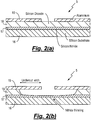
- FIG. 2(a) presents a schematic representation of a blanket film MEMS 5 upon which an HF vapour etch is to be performed.
- the MEMS 5 can be seen to comprise a silicon substrate 16 upon which is located a silicon nitride layer 17, a sacrificial layer of silicon dioxide 18 and an aluminium masking layer 19.
- the MEMS 5 In order to etch the silicon dioxide layer 18 the MEMS 5 is initially located upon the pedestal 15 and the operating temperature and pressure within the process chamber 3 set. The HF and water vapours are then introduced to the process chamber 3 in order to etch the silicon dioxide layer 18, as presented in Figure 2(b) .
- a MEMS 5 comprising a 1 ⁇ m thick layer of HDP silicon dioxide 18, a 220nm thick layer of LPCVD silicon nitride 17 and a 200nm thick aluminium mask 19 was HF vapour etched within the process chamber 3, at an operating temperature of 25°C and at a process chamber pressure of 18T, so as to produce an undercut of 10 ⁇ m.
- the etch approximately 25 minutes
- a hydrogen compound gas e.g. hydrogen gas (H2) from source 7 provides a means for increasing the selectivity to silicon nitride (Si 3 N 4 ) during the hydrogen fluoride (HF) vapour etch of silicon dioxide (SiO 2 ).
- a MEMS again comprising a 1 ⁇ m thick layer of HDP silicon dioxide 18, a 220nm thick layer of LPCVD silicon nitride 17 and a 200nm thick aluminium mask 19 was again HF vapour etched within the process chamber 3, at an operating temperature of 25°C and at a process chamber pressure of 18T, so as to produce an undercut of 10 ⁇ m.
- hydrogen compound gases such as ammonia (NH 3 ), methane (CH 4 ) or ethane (C 2 H 6 ) have alternatively been employed to provide an increased selectivity to the silicon nitride layer 17. In practice the best results have however been achieved using hydrogen gas. It will be appreciated that the hydrogen compound gas may comprise mixtures of two or more of the above mentioned hydrogen gas compounds.
- reducing the operating temperature of the process chamber also provides a means for increasing the selectivity to silicon nitride (Si 3 N 4 ) during the hydrogen fluoride (HF) vapour etch of silicon dioxide (SiO 2 ).
- silicon nitride Si 3 N 4
- HF hydrogen fluoride
- SiO 2 silicon dioxide
- the hydrogen compound gas generally tends to react more readily with the monofluoride species (F - , and HF) of the HF vapour than with the difluoride species (HF 2 - and H 2 F 2 ).
- the introduction of such a secondary gas acts to shift the equilibrium of the HF reactive species towards the difluoride species (HF 2 - and H 2 F 2 ) i.e. the ratio of difluoride reactive species (HF 2 - and H 2 F 2 ) to monofluoride reactive species (F - , and HF) is increased. It is this effect that is believed to lead to the observed increase in the selectivity to silicon nitride (Si 3 N 4 ) during the hydrogen fluoride (HF) vapour etch of silicon dioxide (SiO 2 ).
- a secondary contribution may also be present when ammonia (NH 3 ) is employed as the hydrogen compound gas.
- Reaction equations (3) and (4) show that ammonia (NH 3 ) is produced as a by-product of an HF vapour etch of silicon nitride (Si 3 N 4 ).
- the introduction of ammonia (NH 3 ) tends to prohibit the silicon nitride (Si 3 N 4 ) etch.
- a secondary contribution may also be present when water vapour (H 2 O) is employed as the catalyst.
- water vapour H 2 O
- etching of a sacrificial silicon dioxide (SiO 2 ) portion in a microstructure such as a microelectro-mechanical structures (MEMS) by the use an etchant gas, namely hydrogen fluoride (HF) vapour is performed with greater selectivity to other portions within the MEMS, and in particular portions of silicon nitride (Si 3 N 4 ).
- a secondary non-etchant gas suitable for increase the ratio of difluoride reactive species (HF 2 - and H 2 F 2 ) to monofluoride reactive species (F - , and HF) within the HF vapour.
- the secondary non-etchant gas may comprise a hydrogen compound gas.
- the ratio of difluoride reactive species (HF 2 - and H 2 F 2 ) to the monofluoride reactive species (F - , and HF) within the HF vapour can also be increased by setting an etch operating temperature to below 20oC.
Landscapes
- Engineering & Computer Science (AREA)
- Manufacturing & Machinery (AREA)
- Microelectronics & Electronic Packaging (AREA)
- Chemical & Material Sciences (AREA)
- Physics & Mathematics (AREA)
- Geometry (AREA)
- Chemical Kinetics & Catalysis (AREA)
- General Chemical & Material Sciences (AREA)
- Materials Engineering (AREA)
- Mechanical Engineering (AREA)
- Metallurgy (AREA)
- Organic Chemistry (AREA)
- Drying Of Semiconductors (AREA)
- Micromachines (AREA)
- Formation Of Insulating Films (AREA)
Description
- The present invention relates to a method for improved selectivity to surrounding materials when etching silicon dioxide with a hydrogen fluoride (HF) vapour. In particular, the etch parameters are carefully controlled so as to enhance the selectivity with silicon nitride.
- In the manufacture of microstructures, for example microelectro-mechanical structures (MEMS), etching processes are used to remove sacrificial (i.e. unwanted) areas of material, see for example international patent publication number
WO 2008/015434 and US patent publication numbersUS 2003/0080082 ,US 2006/0216941 andUS 2006/0207968 . MEMS have found applications in inertial measurement, pressure sensing, thermal measurement, micro-fluidics, optics, and radio-frequency communications, and the range of possibilities for these structures continues to grow. Sacrificial layers are initially employed in the construction of the MEMS and then subsequently removed with an etch step, which allows the released structure to operate as designed. In order to produce reliable structures the release etch step is required to remove the sacrificial layer without etching the surrounding material. Ideally the etch of the sacrificial layer should have no impact at all on the remaining structure. - Many materials are known to be employed during the manufacture of MEMS e.g. silicon, silicon dioxide (SiO2), silicon nitride (Si3N4), aluminium and photoresist to name but a few. Some of these materials are employed as the sacrificial materials while others are employed to define and hence form the MEMS. It is not uncommon during the manufacture of a MEMS for more than one sacrificial etch step to be employed. For example a film may initially be employed as a mask during a first sacrificial etch process and then be subsequently etched as the next sacrificial layer. In any release etch it is therefore highly desirable for there to be a high etch selectivity between the sacrificial layer and the surrounding materials.
- A commonly employed approach to quantifying the selectivity of materials is to etch blanket films of those materials using the same etch arrangement and then compare the amount of material that has been removed. This technique is widely used and gives very useful information. However, in practice etch selectivity can be found to be dependent upon the materials present and the manner in which they have been deposited, the etch characteristics itself, and any subsequent treatments carried out on the MEMS.
- By way of example, hydrogen fluoride (HF) vapour etching is commonly used to remove sacrificial areas of silicon dioxide in the manufacture of MEMS. This etch is a chemical etch, with no plasma being required, is performed at a process chamber pressure in the range of 18T to 150T and normally requires heating so as to achieve an operating temperature between 25°C and 70 °C. A catalyst is required for the HF vapour etch of silicon dioxide (SiO2) to proceed. Water (H2O) is often employed as the catalyst since this gives a fast and controlled etch, although alternatively catalysts known in the art include alcohols, methanol, ethanol and propanol. However, water (H2O) (along with silicon tetrafluoride (SiF4)) is a by-product of the reaction process and this means that the inherent etch characteristics can have a significant influence on the etch taking place. Therefore careful control of the process conditions is required.
- The hydrogen fluoride (HF) vapour etching of silicon dioxide is known to exhibit high selectivity to many common films. For example, the theoretical selectivity to silicon and aluminium is high and no etching or corrosion is expected. However, the above described process conditions are also compatible for the hydrogen fluoride (HF) vapour to etch silicon nitride (Si3N4). Therefore in practice it can prove difficult to achieve a high selectivity between silicon dioxide (SiO2) and silicon nitride (Si3N4) layers during a hydrogen fluoride (HF) vapour etch.
- It is therefore an object of an embodiment of the present invention to provide a method for the hydrogen fluoride (HF) vapour etch of silicon dioxide that exhibits increased selectivity to silicon nitride as compared to those techniques known in the art
- There is provided a method of selectively etching silicon dioxide (SiO2) from silicon nitride (Si3N4) within a process chamber so as to produce one or more microstructures, the method comprising:
- providing the process chamber with an etching vapour comprising hydrogen fluoride (HF); and
- increasing a ratio of difluoride reactive species (HF2 - and H2F2) to monofluoride reactive species (F-, and HF) within the etching vapour by setting an etch operating temperature to below 20°C.
- Increasing the ratio of the difluoride reactive species (HF2 - and H2F2) to the monofluoride reactive species (F-, and HF) within the etching vapour acts to significantly increase the selectivity of the etch process to silicon nitride (Si3N4).
- Increasing the ratio of difluoride reactive species (HF2 - and H2F2) to monofluoride reactive species (F-, and HF) within the etching vapour may comprise providing the process chamber with a non-etchant gas.
- Preferably the non-etchant gas comprises a hydrogen compound gas. The hydrogen compound may comprise a compound selected from the group of compounds comprising hydrogen (H2) ammonia (NH3), methane (CH4), ethane (C2H6) or mixtures thereof.
- Preferably the etch operating temperature is set to 10°C.
- Preferably the method further comprises providing the process chamber with a catalyst. The catalyst preferably comprises water (H2O) vapour.
- The method may comprise the control of the amount of etching vapour and non etchant gas within the process chamber by controlling a vacuum pump rate out of the process chamber.
- Alternatively, the method may comprise circulation of the etching vapour and non etchant gas through the process chamber.
- It is preferable for the method to comprise the provision of a mask overlying the silicon dioxide so as to allow for selective etching of the silicon dioxide.
- There may be provided a vapour phase etching apparatus for selectively etching silicon dioxide (SiO2) from silicon nitride (Si3N4) so as to produce one or more microstructures, the apparatus comprising:
- a process chamber for receiving the silicon dioxide to be etched;
- a hydrogen fluoride (HF) vapour source;
- a non-etchant gas source wherein the non-etchant gas is suitable for increasing a ratio of difluoride reactive species (HF2 - and H2F2) to monofluoride reactive species (F-, and HF) within a hydrogen fluoride (HF) vapour; and
- one or more gas lines that connect the hydrogen fluoride (HF) vapour source and the non-etchant gas source to the process chamber.
- The vapour phase etching apparatus may comprise a catalyst source. Preferably the one or more gas lines connect the catalyst source to the process chamber.
- Optionally a carrier gas source may provide a means for transporting the catalyst to the process chamber.
- The catalyst may comprise water. The water may be in vapour form.
- The vapour phase etching apparatus preferably comprises a temperature controller that provides a means for setting an etch operating temperature.
- The vapour phase etching apparatus preferably comprises a vacuum pump connected to the process chamber. The vacuum pump provides a means for controlling the amount of etching vapour and/or non-etchant gas within the process chamber.
- The vapour phase etching apparatus may further comprise one or more flow controllers connected to the one or more gas lines. The one or more flow controllers provide a means for controlling the amount of fluids e.g. the etching vapour and/or non-etchant gas reaching the process chamber.
- Alternatively, the vapour phase etching apparatus is configured so as to recirculate the etching vapour and/or the non etchant gas.
- According to
claim 1 the present invention provides a method of selectively etching silicon dioxide (SiO2) from silicon nitride (Si3N4) in a process chamber so as to produce one or more microstructures, the method comprising: - providing the process chamber with an etching vapour comprising hydrogen fluoride (HF) vapour; and
- setting an etch operating temperature to below 20°C.
- The setting of the etch operating temperature to 20°C or below acts to increase the ratio of difluoride reactive species (HF2 - and H2F2) to monofluoride reactive species (F-, and HF) within the etching vapour and so significantly increases the selectivity of the etch to silicon nitride (Si3N4).
- Preferably the etch operating temperature is set to 10°C.
- The method may further comprise providing the process chamber with a non-etchant gas suitable for increasing a ratio of difluoride reactive species (HF2 - and H2F2) to monofluoride reactive species (F-, and HF) within the etching vapour.
- There will now be described, by way of example only, various embodiments of the invention with reference to the drawings, of which:
-
Figure 1 illustrates in schematic form an HF vapour etch system and -
Figure 2 illustrates in schematic form a blanket film MEMS comprising an aluminium mask, a silicon dioxide layer located on top of a layer of silicon nitride (a) before etching and (b) after etching. - With reference to
Figure 1 , there is presented an hydrogen fluoride (HF)vapour etch system 1 that comprises agas delivery system 2 in fluid communication with aprocess chamber 3. Avacuum pump 4 in fluid communication with theprocess chamber 3 is also provided. This system enables an improved selectivity to silicon nitride (Si3N4) during an HF vapour etch of a sacrificial silicon dioxide (SiO2) layer within aMEMS 5 located within theprocess chamber 3, as will be described in detail below. - The
gas delivery system 2 comprises anHF vapour source 6, ahydrogen gas source 7, awater source 8, avaporiser 9 and twonitrogen gas sources process chamber 3 is produced by connecting thewater source 8 to thevaporiser 9. Thenitrogen gas sources source 10a provides a carrier gas to assist in transporting the water vapour, employed as the catalyst for the HF vapour etch, to theprocess chamber 3 andsource 10b provides a buffer gas for thevapour etch system 1. Mass or liquid flow controllers (MFC) 11 are preferably provided within each supply line of thegas delivery system 2 so as to provide a means for regulating the associated fluid flow. - A
pressure gauge 12 is employed to monitor the pressure within theprocess chamber 3. The pump rate of thevacuum pump 4 and/or the MFCs 11 can be controlled to maintain a set operating pressure within theprocess chamber 3. The use of an adaptive pressure controller (APC) 13 enables accurate control of theprocess chamber 3 pressure. Note that in an alternative embodiment, the gases within theprocess chamber 3 may be circulated, in which case thevacuum pump 4 serves to initially evacuate the process chamber 3 (thus drawing in etchant vapour) or to evacuate theprocess chamber 3 subsequent to completion of the etch step. - A
thermometer 14 is also connected to theprocess chamber 3, and preferably to apedestal 15 located within theprocess chamber 3 upon which theMEMS 5 to be etched is located. When acting in conjunction with a temperature controller these elements provide a means for setting and maintaining an operating temperature for the HF vapour etch. -
Figure 2(a) presents a schematic representation of ablanket film MEMS 5 upon which an HF vapour etch is to be performed. TheMEMS 5 can be seen to comprise asilicon substrate 16 upon which is located asilicon nitride layer 17, a sacrificial layer ofsilicon dioxide 18 and analuminium masking layer 19. - In order to etch the
silicon dioxide layer 18 theMEMS 5 is initially located upon thepedestal 15 and the operating temperature and pressure within theprocess chamber 3 set. The HF and water vapours are then introduced to theprocess chamber 3 in order to etch thesilicon dioxide layer 18, as presented inFigure 2(b) . - In practice there is found to be a high selectivity between the
silicon dioxide layer 18 and thealuminium mask 19 in accordance with theoretical predictions i.e. there is no noticeable etching of thealuminium mask 19. However, the selectivity between thesilicon dioxide layer 18 and thesilicon nitride layer 17 is significantly lower than that with thealuminium mask 19 to the extent that significant levels of etching of thesilicon nitride layer 17 occurs. By way of example, aMEMS 5 comprising a 1µm thick layer ofHDP silicon dioxide 18, a 220nm thick layer ofLPCVD silicon nitride 17 and a 200nmthick aluminium mask 19 was HF vapour etched within theprocess chamber 3, at an operating temperature of 25°C and at a process chamber pressure of 18T, so as to produce an undercut of 10µm. On completion of the etch (approximately 25 minutes) there remained a 200nmthick aluminium mask 19 but only 55nm of thesilicon nitride layer 17 remained, 165nm having been removed by the HF vapour etch. - The applicant has found that the introduction of a hydrogen compound gas e.g. hydrogen gas (H2) from
source 7 provides a means for increasing the selectivity to silicon nitride (Si3N4) during the hydrogen fluoride (HF) vapour etch of silicon dioxide (SiO2). By way of example, a MEMS again comprising a 1µm thick layer ofHDP silicon dioxide 18, a 220nm thick layer ofLPCVD silicon nitride 17 and a 200nmthick aluminium mask 19 was again HF vapour etched within theprocess chamber 3, at an operating temperature of 25°C and at a process chamber pressure of 18T, so as to produce an undercut of 10µm. However, on this occasion 100sccm of hydrogen gas (H2) was also supplied to theprocess chamber 3. On completion of the HF vapour etch (approximately 25 minutes) there again remained a 200nmthick aluminium mask 19 but now the remaining silicon nitride oxide layer was 210nm thick i.e. only 10nm had been removed. This represent a 16.5 times improvement in etch selectivity between thesilicon dioxide layer 18 and thesilicon nitride layer 17 when compared to the same process in the absence of the hydrogen gas. - Other hydrogen compound gases such as ammonia (NH3), methane (CH4) or ethane (C2H6) have alternatively been employed to provide an increased selectivity to the
silicon nitride layer 17. In practice the best results have however been achieved using hydrogen gas. It will be appreciated that the hydrogen compound gas may comprise mixtures of two or more of the above mentioned hydrogen gas compounds. - The applicant has also found that reducing the operating temperature of the process chamber also provides a means for increasing the selectivity to silicon nitride (Si3N4) during the hydrogen fluoride (HF) vapour etch of silicon dioxide (SiO2). On this occasion blanket films on a standard sample were etched and the selectivity at different temperatures investigated. The films employed for these tests comprised thermal silicon dioxide and PECVD silicon nitride layers. Employing the standard recipe at 25°C described above the etch selectivity was 11:1 for these test structure. However, on cooling the test sample to 10°C, and readjusting the chamber pressure to give the same etch rate as above, resulted in the etch selectivity increasing to 38:1.
- Tests across a range temperatures were carried out to further investigate the improvements in the selectivity to silicon nitride during an HF vapour etching of silicon dioxide. Somewhat surprisingly noticeable improvements were observed for operating temperatures as high 20°C.
- It will be appreciated by the skilled reader that the above procedures may be combined i.e. as well as introducing a hydrogen compound gas into the
process chamber 3 the operating temperature may simultaneously be reduced to below 20°C. The overall effect is to further improve the selectivity to silicon nitride during an HF vapour etch of silicon dioxide. - The following is provided by way of explanation of the observed results. Theoretical studies suggest that the main contribution to the etching of silicon dioxide (SiO2) involve the difluoride reactive species within the HF vapour (HF2 - and H2F2) while the main contribution to the etching of silicon nitride (Si3N4) are believed to be the monofluoride reactive species (F-, and HF). These etching processes may be described by the following reaction equations:


- It is believed that the hydrogen compound gas generally tends to react more readily with the monofluoride species (F-, and HF) of the HF vapour than with the difluoride species (HF2 - and H2F2). Thus the introduction of such a secondary gas acts to shift the equilibrium of the HF reactive species towards the difluoride species (HF2 - and H2F2) i.e. the ratio of difluoride reactive species (HF2 - and H2F2) to monofluoride reactive species (F- , and HF) is increased. It is this effect that is believed to lead to the observed increase in the selectivity to silicon nitride (Si3N4) during the hydrogen fluoride (HF) vapour etch of silicon dioxide (SiO2).
- A secondary contribution may also be present when ammonia (NH3) is employed as the hydrogen compound gas. Reaction equations (3) and (4) show that ammonia (NH3) is produced as a by-product of an HF vapour etch of silicon nitride (Si3N4). Thus the introduction of ammonia (NH3) tends to prohibit the silicon nitride (Si3N4) etch.
- Due to entropy effects it is believed that reducing the operating temperature of the HF vapour etch process to below 20°C also results in the equilibrium of the HF reactive species shifting towards the difluoride species (HF2 - and H2F2) i.e. the ratio of difluoride reactive species to monofluoride reactive species is again increased. This again is believed to account for the observed increase in selectivity to silicon nitride (Si3N4) during the hydrogen fluoride (HF) vapour etch of silicon dioxide (SiO2).
- A secondary contribution may also be present when water vapour (H2O) is employed as the catalyst. When the operating temperature is reduced the water vapour starts to condense on the exposed surfaces of the
MEMS 5. Since water vapour (H2O) acts as a catalyst for the HF vapour etch of silicon dioxide (SiO2), reaction equations (1) and (2), it is believed that condensation effects act to increase the silicon dioxide (SiO2) etch relative to the silicon nitride (Si3N4) etch. - As described previously, a number of other factors will affect the performance of an HF vapour etch performance e.g. gas flow rates,
process chamber 3 pressure and the physical structure of the MEMS itself. However, by adding a suitable secondary gas and/or reducing the operating temperature for the HF vapour etch the ratio of the difluoride species (HF2 - and H2F2) to the monofluoride reactive species (F-, and HF) is increased. As a result the applicants have been able to demonstrate significantly improved selectivity to silicon nitride (Si3N4) during the hydrogen fluoride (HF) vapour etch of silicon dioxide (SiO2). Even small amounts of hydrogen gas have been seen to makes a significant difference in this selectivity. - While the above described embodiments employ a vacuum pump which pumps carrier gases, etch vapour, etch by-product and the secondary hydrogen compound gas out of the process chamber, thus creating a flow of etchant and hydrogen there through, it is also envisaged that the etchant and hydrogen compound gas could be recirculated.
- The etching of a sacrificial silicon dioxide (SiO2) portion in a microstructure such as a microelectro-mechanical structures (MEMS) by the use an etchant gas, namely hydrogen fluoride (HF) vapour is performed with greater selectivity to other portions within the MEMS, and in particular portions of silicon nitride (Si3N4). This is achieved by the addition of a secondary non-etchant gas suitable for increase the ratio of difluoride reactive species (HF2 - and H2F2) to monofluoride reactive species (F-, and HF) within the HF vapour. The secondary non-etchant gas may comprise a hydrogen compound gas. The ratio of difluoride reactive species (HF2 - and H2F2) to the monofluoride reactive species (F-, and HF) within the HF vapour can also be increased by setting an etch operating temperature to below 20ºC.
Claims (12)
- A method of selectively etching silicon dioxide (SiO2) (18) from silicon nitride (Si3N4) (17) in a process chamber (3) so as to produce one or more microstructures (5), the method comprising:providing the process chamber (3) with an etching vapour (6) comprising hydrogen fluoride (HF); andcharacterised in thatan etch operating temperature is set to below 20°C.
- A method of selectively etching silicon dioxide (SiO2) (18) from silicon nitride (Si3N4) (17) as claimed in claim 1 wherein the method further comprises providing the process chamber (3) with a non-etchant gas (7).
- A method of selectively etching silicon dioxide (SiO2) (18) from silicon nitride (Si3N4) (17) as claimed in claim 2 wherein the non-etchant gas (7) comprises a hydrogen compound gas.
- A method of selectively etching silicon dioxide (SiO2) (18) from silicon nitride (Si3N4) (17) as claimed in claim 3 wherein the hydrogen compound comprises a compound selected from the group of compounds comprising hydrogen (H2), ammonia (NH3), methane (CH4), ethane (C2H6) and mixtures thereof.
- A method of selectively etching silicon dioxide (SiO2) (18) from silicon nitride (Si3N4) (17) as claimed in any of the preceding claims wherein the etch operating temperature is set to 10°C.
- A method of selectively etching silicon dioxide (SiO2) (18) from silicon nitride (Si3N4) (17) as claimed in any of the preceding claims wherein the method further comprises providing the process chamber with a catalyst (8).
- A method of selectively etching silicon dioxide (SiO2) (18) from silicon nitride (Si3N4) (17) as claimed in claim 6 wherein the catalyst (8) comprises water (H2O) vapour.
- A method of selectively etching silicon dioxide (SiO2) (18) from silicon nitride (Si3N4) (17) as claimed in any of the preceding claims wherein the method further comprises controlling the amount of etching vapour (6) within the process chamber (3) by controlling a vacuum pump rate out of the process chamber (3).
- A method of selectively etching silicon dioxide (SiO2) (18) from silicon nitride (Si3N4) (17) as claimed in any of claims 2 to 8 wherein the method further comprises controlling the amount of non etchant gas (7) within the process chamber (3) by controlling a vacuum pump rate out of the process chamber (3).
- A method of etching silicon dioxide (SiO2) (18) from silicon nitride (Si3N4) (17) as claimed in any of claims 1 to 7 wherein the method comprises circulating the etching vapour (6) through the process chamber (3).
- A method of etching silicon dioxide (SiO2) (18) from silicon nitride (Si3N4) (17) as claimed in any of claims 1 to 7 wherein the method comprises circulating the non etchant gas (7) through the process chamber (3).
- A method of etching silicon dioxide (SiO2) (18) from silicon nitride (Si3N4) (17) as claimed in any of the preceding claims wherein the method comprises the provision of a mask (19) overlying the silicon dioxide (18) so as to allow for selective etching of the silicon dioxide (18).
Applications Claiming Priority (2)
| Application Number | Priority Date | Filing Date | Title |
|---|---|---|---|
| GB1101188.9A GB2487716B (en) | 2011-01-24 | 2011-01-24 | Vapour Etch of Silicon Dioxide with Improved Selectivity |
| PCT/GB2012/050144 WO2012101431A1 (en) | 2011-01-24 | 2012-01-24 | Vapour etch of silicon dioxide with improved selectivity |
Publications (3)
| Publication Number | Publication Date |
|---|---|
| EP2668312A1 EP2668312A1 (en) | 2013-12-04 |
| EP2668312B1 true EP2668312B1 (en) | 2019-11-20 |
| EP2668312B8 EP2668312B8 (en) | 2019-12-25 |
Family
ID=43769521
Family Applications (1)
| Application Number | Title | Priority Date | Filing Date |
|---|---|---|---|
| EP12708367.3A Active EP2668312B8 (en) | 2011-01-24 | 2012-01-24 | Vapour etch of silicon dioxide with improved selectivity |
Country Status (9)
| Country | Link |
|---|---|
| US (1) | US10354884B2 (en) |
| EP (1) | EP2668312B8 (en) |
| JP (1) | JP5864612B2 (en) |
| KR (1) | KR101863178B1 (en) |
| CN (1) | CN103328688B (en) |
| DK (1) | DK2668312T3 (en) |
| ES (1) | ES2767108T3 (en) |
| GB (1) | GB2487716B (en) |
| WO (1) | WO2012101431A1 (en) |
Families Citing this family (19)
| Publication number | Priority date | Publication date | Assignee | Title |
|---|---|---|---|---|
| JP6381332B2 (en) * | 2013-09-19 | 2018-08-29 | 浜松ホトニクス株式会社 | Manufacturing method of semiconductor device |
| JP2016025195A (en) * | 2014-07-18 | 2016-02-08 | 東京エレクトロン株式会社 | Etching method |
| CN105632918A (en) * | 2014-10-30 | 2016-06-01 | 中国科学院微电子研究所 | A method for removing the natural oxide layer before source and drain epitaxy of FinFET devices |
| CN104316577B (en) * | 2014-10-31 | 2016-12-07 | 中国矿业大学 | A kind of methane transducer based on flip chip bonding encapsulation and preparation method and application |
| JP6530289B2 (en) * | 2015-09-11 | 2019-06-12 | 東芝メモリ株式会社 | Analysis pretreatment unit |
| WO2017176027A1 (en) * | 2016-04-05 | 2017-10-12 | 주식회사 테스 | Method for selectively etching silicon oxide film |
| US10497579B2 (en) * | 2017-05-31 | 2019-12-03 | Applied Materials, Inc. | Water-free etching methods |
| CN108847391B (en) * | 2018-06-01 | 2021-06-08 | 北京北方华创微电子装备有限公司 | Non-plasma dry etching method |
| CN110718459A (en) * | 2018-07-13 | 2020-01-21 | 北京北方华创微电子装备有限公司 | Non-plasma etching method and etching equipment |
| GB2580858B (en) * | 2018-09-07 | 2021-07-21 | Memsstar Ltd | A method for detecting defects in thin film layers |
| EP4056000A4 (en) | 2019-11-06 | 2024-05-29 | Ttm Technologies Inc. | SYSTEMS AND METHODS FOR REMOVING UNWANTED METALS IN THROUGH-PLATED PRINTED BOARDS |
| GB202117751D0 (en) | 2019-11-14 | 2022-01-26 | Memsstar Ltd | Method of manufacturing a microstructure |
| CN113785382B (en) * | 2020-04-10 | 2023-10-27 | 株式会社日立高新技术 | Etching method |
| JP7312160B2 (en) * | 2020-12-28 | 2023-07-20 | 株式会社アルバック | Etching apparatus and etching method |
| US11581242B2 (en) * | 2021-01-14 | 2023-02-14 | Tokyo Electron Limited | Integrated high efficiency gate on gate cooling |
| GB2606747B (en) | 2021-05-19 | 2024-11-20 | Memsstar Ltd | Method of manufacturing a microstructure |
| EP4219391A1 (en) | 2022-01-28 | 2023-08-02 | Hahn-Schickard-Gesellschaft für angewandte Forschung e.V. | Through-hole for operating a mems component in a hermetic cavity |
| GB2629555A (en) | 2023-01-25 | 2024-11-06 | Memsstar Ltd | Method of manufacturing a microstructure |
| US20250246437A1 (en) * | 2024-01-26 | 2025-07-31 | Tokyo Electron Limited | Selective etching in semiconductor devices |
Citations (2)
| Publication number | Priority date | Publication date | Assignee | Title |
|---|---|---|---|---|
| US20060207968A1 (en) * | 2005-03-08 | 2006-09-21 | Mumbauer Paul D | Selective etching of oxides from substrates |
| US20060216941A1 (en) * | 2003-04-22 | 2006-09-28 | Kazuhide Hasebe | Method for removing silicon oxide film and processing apparatus |
Family Cites Families (31)
| Publication number | Priority date | Publication date | Assignee | Title |
|---|---|---|---|---|
| JPS53114743A (en) * | 1977-03-18 | 1978-10-06 | Toshiba Corp | Etching method |
| JPS5545019A (en) * | 1978-09-25 | 1980-03-29 | Chiyou Lsi Gijutsu Kenkyu Kumiai | Production of photo mask |
| KR930005440B1 (en) * | 1989-10-02 | 1993-06-21 | 다이닛뽕 스쿠린 세이소오 가부시키가이샤 | Selective removing method of insulate film |
| JPH088231B2 (en) * | 1989-10-02 | 1996-01-29 | 大日本スクリーン製造株式会社 | Selective removal method of insulating film |
| JPH0422123A (en) * | 1990-05-17 | 1992-01-27 | Sharp Corp | Etching method for silicon oxide film |
| US5282925A (en) * | 1992-11-09 | 1994-02-01 | International Business Machines Corporation | Device and method for accurate etching and removal of thin film |
| JPH0786240A (en) * | 1993-09-10 | 1995-03-31 | Hitachi Ltd | Surface treatment equipment |
| JP3373019B2 (en) * | 1993-12-16 | 2003-02-04 | 富士フイルムマイクロデバイス株式会社 | Semiconductor wafer vapor processing equipment |
| KR100237000B1 (en) * | 1996-09-21 | 2000-01-15 | 정선종 | Method for fabricating microstructures by using sacrifical oxide |
| US6048406A (en) | 1997-04-08 | 2000-04-11 | Texas Instruments Incorporated | Benign method for etching silicon dioxide |
| US6432830B1 (en) * | 1998-05-15 | 2002-08-13 | Applied Materials, Inc. | Semiconductor fabrication process |
| DE19941042A1 (en) * | 1999-08-28 | 2001-03-15 | Bosch Gmbh Robert | Process for the production of surface micromechanical structures by etching with a vaporous, hydrofluoric acid-containing etching medium |
| US7041224B2 (en) * | 1999-10-26 | 2006-05-09 | Reflectivity, Inc. | Method for vapor phase etching of silicon |
| US6475917B1 (en) * | 1999-10-28 | 2002-11-05 | Taiwan Semiconductor Manufacturing Company | Method to reduce the metal TiN ARC damage in etching back process |
| JP2001308013A (en) * | 2000-04-20 | 2001-11-02 | Seiko Epson Corp | Exhaust control mechanism for semiconductor manufacturing equipment |
| US6645873B2 (en) * | 2000-06-21 | 2003-11-11 | Asm Japan K.K. | Method for manufacturing a semiconductor device |
| US20040094086A1 (en) * | 2001-03-29 | 2004-05-20 | Keiichi Shimaoka | Production device and production method for silicon-based structure |
| WO2003055791A2 (en) * | 2001-10-17 | 2003-07-10 | Applied Materials, Inc. | Improved etch process for etching microstructures |
| US6666979B2 (en) * | 2001-10-29 | 2003-12-23 | Applied Materials, Inc. | Dry etch release of MEMS structures |
| DE10224859A1 (en) | 2002-06-05 | 2003-12-24 | Fraunhofer Ges Forschung | Production of free-running perchlorate, used as propellant, explosive and oxidant, e.g. in solid propellant or pyrotechnics, involves mixing with anticaking agent, transfer to inert carrier gas stream and hammer milling |
| US7877161B2 (en) * | 2003-03-17 | 2011-01-25 | Tokyo Electron Limited | Method and system for performing a chemical oxide removal process |
| US7625603B2 (en) * | 2003-11-14 | 2009-12-01 | Robert Bosch Gmbh | Crack and residue free conformal deposited silicon oxide with predictable and uniform etching characteristics |
| JP2006261451A (en) * | 2005-03-17 | 2006-09-28 | Sony Corp | Etching method |
| GB0615343D0 (en) * | 2006-08-02 | 2006-09-13 | Point 35 Microstructures Ltd | Improved etch process |
| JP2011501874A (en) * | 2007-09-14 | 2011-01-13 | クォルコム・メムズ・テクノロジーズ・インコーポレーテッド | Etching process used in MEMS manufacturing |
| JP2009094307A (en) * | 2007-10-10 | 2009-04-30 | Tokyo Electron Ltd | Etching method and recording medium |
| US8187486B1 (en) | 2007-12-13 | 2012-05-29 | Novellus Systems, Inc. | Modulating etch selectivity and etch rate of silicon nitride thin films |
| JP5352103B2 (en) * | 2008-03-27 | 2013-11-27 | 東京エレクトロン株式会社 | Heat treatment apparatus and treatment system |
| KR100870914B1 (en) * | 2008-06-03 | 2008-11-28 | 주식회사 테스 | Dry etching method of silicon oxide |
| US7994002B2 (en) * | 2008-11-24 | 2011-08-09 | Applied Materials, Inc. | Method and apparatus for trench and via profile modification |
| GB2473851C (en) * | 2009-09-25 | 2013-08-21 | Memsstar Ltd | Improved selectivity in a xenon difluoride etch process |
-
2011
- 2011-01-24 GB GB1101188.9A patent/GB2487716B/en active Active
-
2012
- 2012-01-24 KR KR1020137021088A patent/KR101863178B1/en active Active
- 2012-01-24 EP EP12708367.3A patent/EP2668312B8/en active Active
- 2012-01-24 WO PCT/GB2012/050144 patent/WO2012101431A1/en not_active Ceased
- 2012-01-24 DK DK12708367.3T patent/DK2668312T3/en active
- 2012-01-24 US US13/980,638 patent/US10354884B2/en active Active
- 2012-01-24 JP JP2013549897A patent/JP5864612B2/en active Active
- 2012-01-24 ES ES12708367T patent/ES2767108T3/en active Active
- 2012-01-24 CN CN201280006276.XA patent/CN103328688B/en active Active
Patent Citations (2)
| Publication number | Priority date | Publication date | Assignee | Title |
|---|---|---|---|---|
| US20060216941A1 (en) * | 2003-04-22 | 2006-09-28 | Kazuhide Hasebe | Method for removing silicon oxide film and processing apparatus |
| US20060207968A1 (en) * | 2005-03-08 | 2006-09-21 | Mumbauer Paul D | Selective etching of oxides from substrates |
Also Published As
| Publication number | Publication date |
|---|---|
| DK2668312T3 (en) | 2020-02-17 |
| ES2767108T3 (en) | 2020-06-16 |
| WO2012101431A1 (en) | 2012-08-02 |
| GB2487716A (en) | 2012-08-08 |
| GB201101188D0 (en) | 2011-03-09 |
| KR101863178B1 (en) | 2018-05-31 |
| JP5864612B2 (en) | 2016-02-17 |
| CN103328688A (en) | 2013-09-25 |
| EP2668312B8 (en) | 2019-12-25 |
| US10354884B2 (en) | 2019-07-16 |
| EP2668312A1 (en) | 2013-12-04 |
| CN103328688B (en) | 2016-03-23 |
| JP2014504805A (en) | 2014-02-24 |
| US20140017901A1 (en) | 2014-01-16 |
| KR20140039163A (en) | 2014-04-01 |
| GB2487716B (en) | 2015-06-03 |
Similar Documents
| Publication | Publication Date | Title |
|---|---|---|
| EP2668312B1 (en) | Vapour etch of silicon dioxide with improved selectivity | |
| US9786526B2 (en) | Selectivity in a xenon difluoride etch process | |
| JP6837302B2 (en) | Methods and equipment for vapor phase chemical dry etching of structures | |
| US20230395400A1 (en) | Etching method and etching apparatus | |
| US20250326634A1 (en) | Method of manufacturing a microstructure | |
| EP4341204B1 (en) | Method of manufacturing a microstructure | |
| US20180029883A1 (en) | Selectivity in a xenon difluoride etch process |
Legal Events
| Date | Code | Title | Description |
|---|---|---|---|
| PUAI | Public reference made under article 153(3) epc to a published international application that has entered the european phase |
Free format text: ORIGINAL CODE: 0009012 |
|
| 17P | Request for examination filed |
Effective date: 20130812 |
|
| AK | Designated contracting states |
Kind code of ref document: A1 Designated state(s): AL AT BE BG CH CY CZ DE DK EE ES FI FR GB GR HR HU IE IS IT LI LT LU LV MC MK MT NL NO PL PT RO RS SE SI SK SM TR |
|
| DAX | Request for extension of the european patent (deleted) | ||
| 17Q | First examination report despatched |
Effective date: 20160401 |
|
| STAA | Information on the status of an ep patent application or granted ep patent |
Free format text: STATUS: EXAMINATION IS IN PROGRESS |
|
| REG | Reference to a national code |
Ref country code: DE Ref legal event code: R079 Ref document number: 602012065795 Country of ref document: DE Free format text: PREVIOUS MAIN CLASS: C23F0001440000 Ipc: H01L0021311000 |
|
| GRAP | Despatch of communication of intention to grant a patent |
Free format text: ORIGINAL CODE: EPIDOSNIGR1 |
|
| STAA | Information on the status of an ep patent application or granted ep patent |
Free format text: STATUS: GRANT OF PATENT IS INTENDED |
|
| RIC1 | Information provided on ipc code assigned before grant |
Ipc: B81C 1/00 20060101ALI20190701BHEP Ipc: H01L 21/311 20060101AFI20190701BHEP |
|
| INTG | Intention to grant announced |
Effective date: 20190725 |
|
| GRAS | Grant fee paid |
Free format text: ORIGINAL CODE: EPIDOSNIGR3 |
|
| GRAA | (expected) grant |
Free format text: ORIGINAL CODE: 0009210 |
|
| STAA | Information on the status of an ep patent application or granted ep patent |
Free format text: STATUS: THE PATENT HAS BEEN GRANTED |
|
| AK | Designated contracting states |
Kind code of ref document: B1 Designated state(s): AL AT BE BG CH CY CZ DE DK EE ES FI FR GB GR HR HU IE IS IT LI LT LU LV MC MK MT NL NO PL PT RO RS SE SI SK SM TR |
|
| REG | Reference to a national code |
Ref country code: GB Ref legal event code: FG4D |
|
| REG | Reference to a national code |
Ref country code: CH Ref legal event code: EP Ref country code: CH Ref legal event code: PK Free format text: BERICHTIGUNG B8 |
|
| RBV | Designated contracting states (corrected) |
Designated state(s): AL AT BE BG CH CY CZ DE DK EE ES FI FR GR HR HU IE IS IT LI LT LU LV MC MK MT NL NO PL PT RO RS SE SI SK SM TR |
|
| REG | Reference to a national code |
Ref country code: DE Ref legal event code: R096 Ref document number: 602012065795 Country of ref document: DE |
|
| REG | Reference to a national code |
Ref country code: IE Ref legal event code: FG4D |
|
| REG | Reference to a national code |
Ref country code: AT Ref legal event code: REF Ref document number: 1205146 Country of ref document: AT Kind code of ref document: T Effective date: 20191215 |
|
| REG | Reference to a national code |
Ref country code: CH Ref legal event code: NV Representative=s name: R.A. EGLI AND CO, PATENTANWAELTE, CH Ref country code: NL Ref legal event code: FP |
|
| RAP2 | Party data changed (patent owner data changed or rights of a patent transferred) |
Owner name: MEMSSTAR LIMITED |
|
| REG | Reference to a national code |
Ref country code: DK Ref legal event code: T3 Effective date: 20200212 |
|
| REG | Reference to a national code |
Ref country code: FI Ref legal event code: FGE |
|
| REG | Reference to a national code |
Ref country code: SE Ref legal event code: TRGR |
|
| REG | Reference to a national code |
Ref country code: LT Ref legal event code: MG4D |
|
| PG25 | Lapsed in a contracting state [announced via postgrant information from national office to epo] |
Ref country code: LV Free format text: LAPSE BECAUSE OF FAILURE TO SUBMIT A TRANSLATION OF THE DESCRIPTION OR TO PAY THE FEE WITHIN THE PRESCRIBED TIME-LIMIT Effective date: 20191120 Ref country code: GR Free format text: LAPSE BECAUSE OF FAILURE TO SUBMIT A TRANSLATION OF THE DESCRIPTION OR TO PAY THE FEE WITHIN THE PRESCRIBED TIME-LIMIT Effective date: 20200221 Ref country code: NO Free format text: LAPSE BECAUSE OF FAILURE TO SUBMIT A TRANSLATION OF THE DESCRIPTION OR TO PAY THE FEE WITHIN THE PRESCRIBED TIME-LIMIT Effective date: 20200220 Ref country code: LT Free format text: LAPSE BECAUSE OF FAILURE TO SUBMIT A TRANSLATION OF THE DESCRIPTION OR TO PAY THE FEE WITHIN THE PRESCRIBED TIME-LIMIT Effective date: 20191120 Ref country code: BG Free format text: LAPSE BECAUSE OF FAILURE TO SUBMIT A TRANSLATION OF THE DESCRIPTION OR TO PAY THE FEE WITHIN THE PRESCRIBED TIME-LIMIT Effective date: 20200220 |
|
| PG25 | Lapsed in a contracting state [announced via postgrant information from national office to epo] |
Ref country code: HR Free format text: LAPSE BECAUSE OF FAILURE TO SUBMIT A TRANSLATION OF THE DESCRIPTION OR TO PAY THE FEE WITHIN THE PRESCRIBED TIME-LIMIT Effective date: 20191120 Ref country code: RS Free format text: LAPSE BECAUSE OF FAILURE TO SUBMIT A TRANSLATION OF THE DESCRIPTION OR TO PAY THE FEE WITHIN THE PRESCRIBED TIME-LIMIT Effective date: 20191120 Ref country code: IS Free format text: LAPSE BECAUSE OF FAILURE TO SUBMIT A TRANSLATION OF THE DESCRIPTION OR TO PAY THE FEE WITHIN THE PRESCRIBED TIME-LIMIT Effective date: 20200320 |
|
| REG | Reference to a national code |
Ref country code: ES Ref legal event code: FG2A Ref document number: 2767108 Country of ref document: ES Kind code of ref document: T3 Effective date: 20200616 |
|
| PG25 | Lapsed in a contracting state [announced via postgrant information from national office to epo] |
Ref country code: AL Free format text: LAPSE BECAUSE OF FAILURE TO SUBMIT A TRANSLATION OF THE DESCRIPTION OR TO PAY THE FEE WITHIN THE PRESCRIBED TIME-LIMIT Effective date: 20191120 |
|
| PG25 | Lapsed in a contracting state [announced via postgrant information from national office to epo] |
Ref country code: EE Free format text: LAPSE BECAUSE OF FAILURE TO SUBMIT A TRANSLATION OF THE DESCRIPTION OR TO PAY THE FEE WITHIN THE PRESCRIBED TIME-LIMIT Effective date: 20191120 Ref country code: PT Free format text: LAPSE BECAUSE OF FAILURE TO SUBMIT A TRANSLATION OF THE DESCRIPTION OR TO PAY THE FEE WITHIN THE PRESCRIBED TIME-LIMIT Effective date: 20200412 Ref country code: CZ Free format text: LAPSE BECAUSE OF FAILURE TO SUBMIT A TRANSLATION OF THE DESCRIPTION OR TO PAY THE FEE WITHIN THE PRESCRIBED TIME-LIMIT Effective date: 20191120 Ref country code: RO Free format text: LAPSE BECAUSE OF FAILURE TO SUBMIT A TRANSLATION OF THE DESCRIPTION OR TO PAY THE FEE WITHIN THE PRESCRIBED TIME-LIMIT Effective date: 20191120 |
|
| REG | Reference to a national code |
Ref country code: DE Ref legal event code: R097 Ref document number: 602012065795 Country of ref document: DE |
|
| PG25 | Lapsed in a contracting state [announced via postgrant information from national office to epo] |
Ref country code: SM Free format text: LAPSE BECAUSE OF FAILURE TO SUBMIT A TRANSLATION OF THE DESCRIPTION OR TO PAY THE FEE WITHIN THE PRESCRIBED TIME-LIMIT Effective date: 20191120 Ref country code: SK Free format text: LAPSE BECAUSE OF FAILURE TO SUBMIT A TRANSLATION OF THE DESCRIPTION OR TO PAY THE FEE WITHIN THE PRESCRIBED TIME-LIMIT Effective date: 20191120 Ref country code: MC Free format text: LAPSE BECAUSE OF FAILURE TO SUBMIT A TRANSLATION OF THE DESCRIPTION OR TO PAY THE FEE WITHIN THE PRESCRIBED TIME-LIMIT Effective date: 20191120 |
|
| PLBE | No opposition filed within time limit |
Free format text: ORIGINAL CODE: 0009261 |
|
| STAA | Information on the status of an ep patent application or granted ep patent |
Free format text: STATUS: NO OPPOSITION FILED WITHIN TIME LIMIT |
|
| 26N | No opposition filed |
Effective date: 20200821 |
|
| PG25 | Lapsed in a contracting state [announced via postgrant information from national office to epo] |
Ref country code: LU Free format text: LAPSE BECAUSE OF NON-PAYMENT OF DUE FEES Effective date: 20200124 |
|
| PG25 | Lapsed in a contracting state [announced via postgrant information from national office to epo] |
Ref country code: PL Free format text: LAPSE BECAUSE OF FAILURE TO SUBMIT A TRANSLATION OF THE DESCRIPTION OR TO PAY THE FEE WITHIN THE PRESCRIBED TIME-LIMIT Effective date: 20191120 Ref country code: SI Free format text: LAPSE BECAUSE OF FAILURE TO SUBMIT A TRANSLATION OF THE DESCRIPTION OR TO PAY THE FEE WITHIN THE PRESCRIBED TIME-LIMIT Effective date: 20191120 |
|
| PG25 | Lapsed in a contracting state [announced via postgrant information from national office to epo] |
Ref country code: TR Free format text: LAPSE BECAUSE OF FAILURE TO SUBMIT A TRANSLATION OF THE DESCRIPTION OR TO PAY THE FEE WITHIN THE PRESCRIBED TIME-LIMIT Effective date: 20191120 Ref country code: MT Free format text: LAPSE BECAUSE OF FAILURE TO SUBMIT A TRANSLATION OF THE DESCRIPTION OR TO PAY THE FEE WITHIN THE PRESCRIBED TIME-LIMIT Effective date: 20191120 Ref country code: CY Free format text: LAPSE BECAUSE OF FAILURE TO SUBMIT A TRANSLATION OF THE DESCRIPTION OR TO PAY THE FEE WITHIN THE PRESCRIBED TIME-LIMIT Effective date: 20191120 |
|
| PG25 | Lapsed in a contracting state [announced via postgrant information from national office to epo] |
Ref country code: MK Free format text: LAPSE BECAUSE OF FAILURE TO SUBMIT A TRANSLATION OF THE DESCRIPTION OR TO PAY THE FEE WITHIN THE PRESCRIBED TIME-LIMIT Effective date: 20191120 |
|
| P01 | Opt-out of the competence of the unified patent court (upc) registered |
Effective date: 20231219 |
|
| REG | Reference to a national code |
Ref country code: AT Ref legal event code: UEP Ref document number: 1205146 Country of ref document: AT Kind code of ref document: T Effective date: 20191120 |
|
| PGFP | Annual fee paid to national office [announced via postgrant information from national office to epo] |
Ref country code: CH Payment date: 20250501 Year of fee payment: 14 |
|
| PGFP | Annual fee paid to national office [announced via postgrant information from national office to epo] |
Ref country code: DK Payment date: 20251209 Year of fee payment: 15 |
|
| PGFP | Annual fee paid to national office [announced via postgrant information from national office to epo] |
Ref country code: FR Payment date: 20251210 Year of fee payment: 15 |
|
| PGFP | Annual fee paid to national office [announced via postgrant information from national office to epo] |
Ref country code: SE Payment date: 20251209 Year of fee payment: 15 |
|
| PGFP | Annual fee paid to national office [announced via postgrant information from national office to epo] |
Ref country code: IE Payment date: 20251209 Year of fee payment: 15 |
|
| PGFP | Annual fee paid to national office [announced via postgrant information from national office to epo] |
Ref country code: NL Payment date: 20260126 Year of fee payment: 15 |
|
| PGFP | Annual fee paid to national office [announced via postgrant information from national office to epo] |
Ref country code: ES Payment date: 20260203 Year of fee payment: 15 |
|
| PGFP | Annual fee paid to national office [announced via postgrant information from national office to epo] |
Ref country code: DE Payment date: 20260131 Year of fee payment: 15 |
|
| PGFP | Annual fee paid to national office [announced via postgrant information from national office to epo] |
Ref country code: AT Payment date: 20260127 Year of fee payment: 15 |
|
| PGFP | Annual fee paid to national office [announced via postgrant information from national office to epo] |
Ref country code: BE Payment date: 20260122 Year of fee payment: 15 Ref country code: FI Payment date: 20260121 Year of fee payment: 15 Ref country code: IT Payment date: 20260105 Year of fee payment: 15 |