EP2665083A2 - Scanning microscope having an adaptive scan - Google Patents
Scanning microscope having an adaptive scan Download PDFInfo
- Publication number
- EP2665083A2 EP2665083A2 EP13167952.4A EP13167952A EP2665083A2 EP 2665083 A2 EP2665083 A2 EP 2665083A2 EP 13167952 A EP13167952 A EP 13167952A EP 2665083 A2 EP2665083 A2 EP 2665083A2
- Authority
- EP
- European Patent Office
- Prior art keywords
- pixels
- regions
- scans
- area
- scanning
- Prior art date
- Legal status (The legal status is an assumption and is not a legal conclusion. Google has not performed a legal analysis and makes no representation as to the accuracy of the status listed.)
- Withdrawn
Links
- 230000003044 adaptive effect Effects 0.000 title description 2
- 238000000034 method Methods 0.000 claims abstract description 41
- 239000002245 particle Substances 0.000 claims description 17
- 239000000463 material Substances 0.000 claims description 13
- 230000004044 response Effects 0.000 claims description 3
- 238000010884 ion-beam technique Methods 0.000 description 15
- 210000004027 cell Anatomy 0.000 description 12
- 238000010894 electron beam technology Methods 0.000 description 12
- 230000009977 dual effect Effects 0.000 description 11
- 230000008569 process Effects 0.000 description 10
- 238000003384 imaging method Methods 0.000 description 8
- 238000005259 measurement Methods 0.000 description 7
- 210000005253 yeast cell Anatomy 0.000 description 6
- 239000004593 Epoxy Substances 0.000 description 5
- 230000002596 correlated effect Effects 0.000 description 5
- 230000006870 function Effects 0.000 description 5
- 241001270131 Agaricus moelleri Species 0.000 description 4
- 230000015572 biosynthetic process Effects 0.000 description 3
- 230000000875 corresponding effect Effects 0.000 description 3
- 238000013479 data entry Methods 0.000 description 3
- 238000004519 manufacturing process Methods 0.000 description 3
- 239000000203 mixture Substances 0.000 description 3
- 230000008021 deposition Effects 0.000 description 2
- 230000008030 elimination Effects 0.000 description 2
- 238000003379 elimination reaction Methods 0.000 description 2
- 238000011156 evaluation Methods 0.000 description 2
- 238000001000 micrograph Methods 0.000 description 2
- 210000000056 organ Anatomy 0.000 description 2
- 238000012545 processing Methods 0.000 description 2
- 238000005086 pumping Methods 0.000 description 2
- 230000004043 responsiveness Effects 0.000 description 2
- ZCYVEMRRCGMTRW-UHFFFAOYSA-N 7553-56-2 Chemical compound [I] ZCYVEMRRCGMTRW-UHFFFAOYSA-N 0.000 description 1
- GYHNNYVSQQEPJS-UHFFFAOYSA-N Gallium Chemical compound [Ga] GYHNNYVSQQEPJS-UHFFFAOYSA-N 0.000 description 1
- 108010083687 Ion Pumps Proteins 0.000 description 1
- 230000001133 acceleration Effects 0.000 description 1
- 230000004075 alteration Effects 0.000 description 1
- 238000010276 construction Methods 0.000 description 1
- 230000001276 controlling effect Effects 0.000 description 1
- 238000013480 data collection Methods 0.000 description 1
- 230000000694 effects Effects 0.000 description 1
- 238000005530 etching Methods 0.000 description 1
- 229910052733 gallium Inorganic materials 0.000 description 1
- 238000002347 injection Methods 0.000 description 1
- 239000007924 injection Substances 0.000 description 1
- 229910052500 inorganic mineral Inorganic materials 0.000 description 1
- 239000011630 iodine Substances 0.000 description 1
- 229910052740 iodine Inorganic materials 0.000 description 1
- 239000002609 medium Substances 0.000 description 1
- 239000012528 membrane Substances 0.000 description 1
- 229910052751 metal Inorganic materials 0.000 description 1
- 239000002184 metal Substances 0.000 description 1
- 229910021645 metal ion Inorganic materials 0.000 description 1
- 239000011707 mineral Substances 0.000 description 1
- 238000012986 modification Methods 0.000 description 1
- 230000004048 modification Effects 0.000 description 1
- 239000012120 mounting media Substances 0.000 description 1
- 230000003287 optical effect Effects 0.000 description 1
- 150000002902 organometallic compounds Chemical class 0.000 description 1
- 239000002243 precursor Substances 0.000 description 1
- 230000000979 retarding effect Effects 0.000 description 1
- 238000001878 scanning electron micrograph Methods 0.000 description 1
- 239000007787 solid Substances 0.000 description 1
- 238000000992 sputter etching Methods 0.000 description 1
- 239000000126 substance Substances 0.000 description 1
- 238000006467 substitution reaction Methods 0.000 description 1
- 238000012546 transfer Methods 0.000 description 1
Images




Classifications
-
- G—PHYSICS
- G02—OPTICS
- G02B—OPTICAL ELEMENTS, SYSTEMS OR APPARATUS
- G02B21/00—Microscopes
- G02B21/0004—Microscopes specially adapted for specific applications
- G02B21/002—Scanning microscopes
-
- H—ELECTRICITY
- H01—ELECTRIC ELEMENTS
- H01J—ELECTRIC DISCHARGE TUBES OR DISCHARGE LAMPS
- H01J37/00—Discharge tubes with provision for introducing objects or material to be exposed to the discharge, e.g. for the purpose of examination or processing thereof
- H01J37/02—Details
- H01J37/22—Optical, image processing or photographic arrangements associated with the tube
- H01J37/222—Image processing arrangements associated with the tube
-
- H—ELECTRICITY
- H01—ELECTRIC ELEMENTS
- H01J—ELECTRIC DISCHARGE TUBES OR DISCHARGE LAMPS
- H01J37/00—Discharge tubes with provision for introducing objects or material to be exposed to the discharge, e.g. for the purpose of examination or processing thereof
- H01J37/26—Electron or ion microscopes; Electron or ion diffraction tubes
- H01J37/261—Details
- H01J37/265—Controlling the tube; circuit arrangements adapted to a particular application not otherwise provided, e.g. bright-field-dark-field illumination
-
- H—ELECTRICITY
- H01—ELECTRIC ELEMENTS
- H01J—ELECTRIC DISCHARGE TUBES OR DISCHARGE LAMPS
- H01J37/00—Discharge tubes with provision for introducing objects or material to be exposed to the discharge, e.g. for the purpose of examination or processing thereof
- H01J37/26—Electron or ion microscopes; Electron or ion diffraction tubes
- H01J37/28—Electron or ion microscopes; Electron or ion diffraction tubes with scanning beams
-
- H—ELECTRICITY
- H04—ELECTRIC COMMUNICATION TECHNIQUE
- H04N—PICTORIAL COMMUNICATION, e.g. TELEVISION
- H04N7/00—Television systems
- H04N7/18—Closed-circuit television [CCTV] systems, i.e. systems in which the video signal is not broadcast
-
- C—CHEMISTRY; METALLURGY
- C07—ORGANIC CHEMISTRY
- C07K—PEPTIDES
- C07K14/00—Peptides having more than 20 amino acids; Gastrins; Somatostatins; Melanotropins; Derivatives thereof
- C07K14/415—Peptides having more than 20 amino acids; Gastrins; Somatostatins; Melanotropins; Derivatives thereof from plants
-
- C—CHEMISTRY; METALLURGY
- C12—BIOCHEMISTRY; BEER; SPIRITS; WINE; VINEGAR; MICROBIOLOGY; ENZYMOLOGY; MUTATION OR GENETIC ENGINEERING
- C12N—MICROORGANISMS OR ENZYMES; COMPOSITIONS THEREOF; PROPAGATING, PRESERVING, OR MAINTAINING MICROORGANISMS; MUTATION OR GENETIC ENGINEERING; CULTURE MEDIA
- C12N15/00—Mutation or genetic engineering; DNA or RNA concerning genetic engineering, vectors, e.g. plasmids, or their isolation, preparation or purification; Use of hosts therefor
- C12N15/09—Recombinant DNA-technology
- C12N15/63—Introduction of foreign genetic material using vectors; Vectors; Use of hosts therefor; Regulation of expression
- C12N15/79—Vectors or expression systems specially adapted for eukaryotic hosts
- C12N15/82—Vectors or expression systems specially adapted for eukaryotic hosts for plant cells, e.g. plant artificial chromosomes (PACs)
- C12N15/8241—Phenotypically and genetically modified plants via recombinant DNA technology
- C12N15/8242—Phenotypically and genetically modified plants via recombinant DNA technology with non-agronomic quality (output) traits, e.g. for industrial processing; Value added, non-agronomic traits
- C12N15/8243—Phenotypically and genetically modified plants via recombinant DNA technology with non-agronomic quality (output) traits, e.g. for industrial processing; Value added, non-agronomic traits involving biosynthetic or metabolic pathways, i.e. metabolic engineering, e.g. nicotine, caffeine
- C12N15/8247—Phenotypically and genetically modified plants via recombinant DNA technology with non-agronomic quality (output) traits, e.g. for industrial processing; Value added, non-agronomic traits involving biosynthetic or metabolic pathways, i.e. metabolic engineering, e.g. nicotine, caffeine involving modified lipid metabolism, e.g. seed oil composition
-
- H—ELECTRICITY
- H01—ELECTRIC ELEMENTS
- H01J—ELECTRIC DISCHARGE TUBES OR DISCHARGE LAMPS
- H01J2237/00—Discharge tubes exposing object to beam, e.g. for analysis treatment, etching, imaging
- H01J2237/26—Electron or ion microscopes
- H01J2237/28—Scanning microscopes
- H01J2237/2813—Scanning microscopes characterised by the application
Definitions
- the present invention relates to a method and an apparatus incorporating the method for adaptive scanning in a scanning microscope.
- a scanning electron microscope (SEM)/focused ion beam (FIB) dual beam device is an increasingly useful tool in the fields of biology (examination of tissue) and natural resource exploitation (examination of core samples).
- SEM scanning electron microscope
- FIB focused ion beam
- This process may entail the collection of an immense amount of data, typically in the giga pixel range. This data collection can be very time-consuming, taking anywhere from 4 to 60 hours. Having to wait such a long period of time can represent a major roadblock to researchers attempting to learn more about the nature of a problem as quickly as possible. Moreover, it limits the throughput of a device.
- Embodiments of a method and apparatus are provided herein for scanning a specimen to form digital imagery, with a set of guide data initially gathered and used to eliminate from further scanning regions of the specimen that are determined to be not of interest.
- the elimination from scanning of the regions that are not of interest speeds up scanning, making the process more efficient.
- the present invention may take the form of a method of using a scanning microscope to rapidly form a digital image of an area.
- the method includes performing an initial set of scans to form a guide pixel set for the area and using the guide pixel set to identify regions representing structures of interest in the area. Then, performing additional scans of the regions representing structures of interest, to gather further data to further evaluate pixels in the regions, and not scanning elsewhere in the area.
- the present invention may take the form of a scanning microscope assembly, adapted to perform a scan of an area, and as a part of performing the scan of the area, adapted to perform an initial set of scans to form a guide pixel set for the area and then to use the guide pixel set to identify regions representing structures of interest in the area. Then, the microscope performs additional scans of the regions representing structures of interest, to gather further data to further evaluate pixels in the regions, and does not scan elsewhere in the area.
- the present invention may take the form of a method of forming an image of an area containing regions of interest and regions not of interest using a scanning imaging device.
- the method includes performing a brief scan, thereby collecting less accurate information than possible, but also taking less time and using data from the brief scan to determine pixels representing regions not of interest. Then, performing a scan at a slower rate, but not scanning pixels determined to represent regions not of interest, thereby completing the scan more quickly.
- the present invention may take the form of a scanning electron microscope assembly including a data entry sub-assembly, adapted to permit a user to input dimensional characteristics of structures of interest in a specimen to be scanned, and wherein the dimensional characteristics affect scanning of the specimen.
- FIG. 1 shows a micrograph of yeast cells set in epoxy
- FIG. 2 shows a micrograph of shale interspersed with other mineral substance
- FIG. 3 shows a probability density function of an actual pixel grayscale, given a pixel sample grayscale value, and a threshold set to yield a low probability of falsely finding a low pixel grayscale
- FIG. 4 shows a probability density function of an actual pixel grayscale, given an averaged set of pixel sample grayscale values and a threshold set to yield a low probability of falsely finding a low pixel grayscale
- FIG. 5 shows a probability density function of an actual pixel grayscale, given an averaged set of pixel sample grayscale values, wherein the set contains more sample values than the set of FIG. 4 , and a threshold set to yield a low probability of falsely finding a low pixel grayscale;
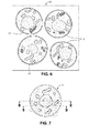
- FIG. 6 shows a set of four yeast cells, set in a solid medium and shown in cross-section
- FIG. 7 shows a top view of a yeast cell, having a transparent outer membrane so that the cell organs are visible.
- FIG. 8 shows a side-section view of the yeast cell of FIG. 7 , taken along line 8-8 of FIG. 7 .
- FIG. 9 shows a side-section view of the yeast cell of FIG. 7 , taken along line 9-9 of FIG. 7 .
- FIG. 10 shows an exemplary dual beam FIB/SEM system that could be used to implement preferred embodiments of the present invention.
- Embodiments of the present invention are directed to methods and apparatuses incorporating methods that reduce the number of data samples that must be acquired in forming an image of a volume.
- One preferred embodiment relies on the fact that typically in an imaged volume there may be specific portions, representing structures of interest, with the rest of the image data being of little or no value.
- the cells 10 are structures of interest whereas the epoxy mounting medium 12, appearing as a field of light gray in the image is not of interest.
- the shale 20 is of interest, whereas the interstitial material 22 which appears as a field of white is not of interest.
- each pixel grayscale in a first scan or a first set of scans can be compared to a threshold to make the determination, which is then applied to subsequent scans of the integrated scan.
- previously imaged surfaces may have areas that are within the same structure of interest. A biological structure, for example, may extend through many of the progressively revealed surfaces.
- a determination may be made as to the location of structures of interest in the previous surface, and this information may be used, together with the initial scan data of an integrated scan, to find these structures of interest in surface currently being imaged. Finally, within a single scan, previously scanned pixels may be correlated with prospectively scanned pixels.
- a scanning electron microscope forms an image by scanning a specimen area multiple (e. g. 20) times with an electron beam while secondary electrons are collected by a secondary electron detector to form an image of the specimen area. This is done to prevent a buildup of charge in any specimen location as the beam dwells at the location.
- For each scan there is a measurement of the responsiveness to the beam, that is, the number of secondary electrons collected, for each pixel (that is, a measurement of true pixel grayscale).
- these pixel grayscale measurements can be compared to a threshold, to determine if some are of a low enough value that they can be fairly presumed to be from a region that is not of interest. But, referring to FIG.
- each such measurement 110 (of a measured value that is exactly at a true pixel grayscale theoretical threshold), has a fairly wide error probability density function (PDF) 112, indicating that it is fairly likely that the actual pixel grayscale is considerably higher than the pixel grayscale measurement.
- PDF error probability density function
- the error PDF 112 is narrowed and the threshold 114 can be reduced, thereby eliminating more pixels from future scanning.
- the PDF is reduced in width still further, as shown in FIG. 5 , and a still tighter threshold 114 may be used without too great a chance of excluding a pixel that is actually more intense than indicated by initial scanning.
- this process is continued until either a predetermined number of scans have been performed, or the number of additional pixels excluded by the process falls below a predetermined level.
- the end of pixel elimination is not necessarily the end of scanning, however, because it may be desirable to continue to collect data to more precisely evaluate pixel grayscales in the regions of interest.
- a region having a particularly variegated scan response is scanned an additional number of times, beyond the standard number of scans in an integrated scan, so that even more precise pixel grayscales may be formed in that region.
- pixels are eliminated from future scanning only after an initial scan, of the integrated scanning process.
- closed forms are detected and included in future scanning, while pixels not inside a closed form are eliminated from future scanning.
- the FIB cuts away a partial layer of material and an SEM images the exposed surface. After the initial surface has been imaged, it can be used as a guide, giving a preliminary indication of the location of structures of interest in the immediately subsequent scan.
- Many specimens include structures of interest that are regularly shaped (for example cells, in a biological specimen) and are larger than the spacing between imaged planes. Accordingly, a pixel occurring outside of a structure of interest in a first imaged plane yields a good indication that the same will be true of a corresponding pixel in a neighboring plane. This information is merged with the information from the first scan or scans from the integrated scanning, to provide an enhanced indicator for whether or not a pixel should be included in a subsequent scan.
- FIGS. 6-9 illustrate this point, with FIG. 6 showing a set of four yeast cells set into epoxy, FIG. 7 showing a top view of the upper left one of these cells, and FIGS. 8 and 9 showing closely spaced sections of the cell of FIG. 7 , taken along planes 8-8 and 9-9 defined in FIG. 7 .
- a preferred embodiment relies on a correlation between data from a first image plane as illustrated in FIG. 8 , and a second image plane as shown in FIGS. 9 , for the cell 12. As can be seen, there is a general similarity between the two slices, due to their close proximity. This similarity can be harvested by correlating pixels from the cut of FIG. 8 , with the prospective evaluation of nearby pixels in the next frame ( FIG. 9 ).
- the first level effort is to aid in the determination of which pixels represent mere epoxy, as opposed to cell matter 12, and to avoid scanning those areas past the first scan of an integrated scan.
- this correlation factor is continued for pixels near the margins of cell 12 as these are the areas have a greater likelihood of not reflecting the region-of-interest value (true or false) of the similarly positioned pixel in the previously scanned plane.
- pixels that are within the cell boundary are given a very high correlation (0.85) for region-of-interest value in the next plane, and this value declines linearly until a distance of twenty pixels from the cell boundary is reached.
- pixel grayscales may be used to gain a faster evaluation of pixel grayscales in the next scan, for example when a cell organ 30 appears in both scans and is generally the same material.
- a scan other than a straight raster scan is made. For example, a spaced [[a ]]scan of every tenth row and column of pixels may help determine where the regions of interest are, before performing more detailed scans.
- the pixel variance in an area about the pixel of interest may be used to determine the presence of a region of interest. This is because a region of interest will tend to have more features than does a background area, such as a volume of undifferentiated epoxy.
- the following thresholding inequality is used to determine which pixels to scan: T ⁇ C R * R + C PSF * Prev Surface Factor + * ⁇ C SP ⁇ SP .
- further scanning for each pixel is stopped when the measurement error for that pixel falls below a threshold. That is, when by taking into account previous surface information, information from previous scans in an integrated scan and previously scanned pixels in the same plane, the system can be certain the pixel's value has been determined to less than a predetermined tolerance, it is not scanned again.
- C R , C PSF , C SP , C V and are set according to the type of material to be imaged and the orientation of internal features, which can be entered by a user. For example, if a material having a lot of long features running through the image planes is to be imaged, C PSF is set relatively high, and ⁇ is set relatively low.
- a user may introduce the material type and orientation of internal features (where appropriate), by a user interface, for example a drop down menu, that would list, for example tissue types, types of core samples. Another drop down menu permits selection of orientation.
- structure of interest for example, cell boundaries are detected using either early scans from an integrated scan, previous surface information and/or same scan information.
- the areas within the boundaries are scanned further, while the areas outside the boundaries are not.
- FIG. 10 shows an exemplary dual beam FIB/SEM system 1010 that could be used to implement preferred embodiments of the present invention. While reference is made to a dual beam system, aspects of the present invention are not limited to a dual beam system, but may also be implemented in other charged particle beam systems, such as single beam systems.
- One embodiment of the present invention utilizes a dual beam FIB/SEM system 1010 that uses an ion beam that is either normal or tilted by a few degrees to the plane of the sample surface and an electron beam having an axis that is also tilted, e.g., fifty-two degrees from the axis of ion beam.
- the ion beam and electron beam are capable of aligning so that the fields of view of both beams are coincident to within a few microns or less.
- the ion beam is typically used to image and machine the work piece, and the electron beam is used primarily for imaging but can also be used for some modification of the work piece.
- the electron beam will typically produce an image of a higher resolution than the ion beam image, and it will not damage the viewed surface like the ion beam.
- the image formed by the two beams can look different, and the two beams can therefore provide more information than a single beam.
- Such a dual beam system could be made from discrete components or alternatively, could be derived from a conventional device such as an AlturaTM or an ExpidaTM system available from FEI Company of Hillsboro, Oregon.
- the present invention could also be implemented using other particle beam systems, including for example, single beam systems, such as FIB or SEM only systems, or dual beam systems having two FIB columns.
- Focused ion beam system 1010 includes an evacuated envelope 1011 having an upper neck portion 1012 within which are located an ion source 1014 and a focusing column 1016 including extractor electrodes and an electrostatic optical system.
- Ion beam 1018 passes from ion source 1014 through column 1016 and between electrostatic deflection means schematically indicated at 1020 toward sample 1022 positioned on movable X-Y-Z stage 1024 within lower chamber 1026.
- An ion pump or other pumping system can be employed to evacuate neck portion 1012.
- the chamber 1026 is evacuated with turbomolecular and mechanical pumping system 1030 under the control of vacuum controller 1032.
- the vacuum system provides within chamber 1026 a vacuum of between approximately 1 x 10 -7 Torr and 5 x 10 -4 Torr. If an etch assisting, an etch retarding gas, or a deposition precursor gas is used, the chamber background pressure may rise, typically to about 1 x 10 -5 Torr.
- High voltage power supply 1034 is connected to ion source 1014 as well as to appropriate electrodes in focusing column 1016 for forming an ion beam 1018 and directing the same downwardly.
- Deflection controller and amplifier 1036 operated in accordance with a prescribed pattern provided by pattern generator 1038, is coupled to deflection plates 1020 whereby beam 1018 may be controlled to trace out a corresponding pattern on the upper surface of sample 1022.
- the deflection plates are placed before the final lens, as is well known in the art.
- the ion source 1014 typically provides a metal ion beam of gallium, although other ion sources, such as a multicusp or other plasma ion source, can be used.
- the ion source 1014 typically is capable of being focused into a sub one-tenth micron wide beam at sample 1022 for either modifying the sample 1022 by ion milling, enhanced etch, material deposition, or for the purpose of imaging the sample 1022.
- a charged particle multiplier 1040 used for detecting secondary ion or electron emission for imaging is connected to signal processor 1042, where the signal from charged particle multiplier 1040 are amplified, converted into digital signals, and subjected to signal processing. The resulting digital signal is to display an image of sample 1022 on the monitor 1044.
- An electron beam 1043 is emitted from a cathode 1052 by applying voltage between cathode 1052 and an anode 1054.
- Electron beam 1043 is focused to a fine spot by means of a condensing lens 1056 and an objective lens 1058.
- Electron beam 1043 is scanned two-dimensionally on the specimen by means of a deflection coil 1060. Operation of condensing lens 1056, objective lens 1058, and deflection coil 1060 is controlled by power supply and control unit 1045.
- Electron beam 1043 can be focused onto sample 1022, which is on movable X-Y-Z stage 1024 within lower chamber 1026.
- Scanning electron microscope 1041 produces a finely focused electron beam 1043, which is scanned across the surface of the structure, preferably in a raster pattern.
- secondary electrons and backscattered electrons are emitted.
- these electrons are detected by secondary electron detector 1040 or backscattered electron detector 1062.
- the analog signal produced either by secondary electron detector 1140 or backscattered electron detector 1062 is amplified and converted into a digital brightness value by signal processor unit 1042.
- the resulting digital signal can be displayed as an image of sample 1022 on the monitor 1044.
- a door 1070 is opened for inserting sample 1022 onto stage 1024, which may be heated or cooled, and also for servicing an internal gas supply reservoir, if one is used.
- the door is interlocked so that it cannot be opened if the system is under vacuum.
- the high voltage power supply provides an appropriate acceleration voltage to electrodes in ion beam column 1016 for energizing and focusing ion beam 1018.
- a gas delivery system 1046 extends into lower chamber 1026 for introducing and directing a gaseous vapor toward sample 1122.
- Another gas delivery system is described in U.S. Pat. No. 5,435,850 to Rasmussen for a "Gas Injection System,” also assigned to the assignee of the present invention.
- iodine can be delivered to enhance etching, or a metal organic compound can be delivered to deposit a metal.
- System controller 1019 controls the operations of the various parts of dual beam system 1010. Through system controller 1019, a user can cause ion beam 1018 or electron beam 1043 to be scanned in a desired manner through commands entered into a conventional user interface (not shown).
- System controller 1019 can also comprise computer-readable memory 1021 and may control dual beam system 1010 in accordance with data or programmed instructions stored in memory 1021.
- CAD data concerning the sample or stored in memory 1021 can be used to create a CAD polygon overlay or other positional data used to locate a feature of interest and alignment points or transfer fiducials as described above.
- a method of using a scanning microscope to rapidly form a digital image of an area comprises performing an initial set of scans to form a guide pixel set for said area, using said guide pixel set to identify regions representing structures of interest in said area, and performing additional scans of said regions representing structures of interest, to gather further data to further evaluate pixels in said regions, and not scanning elsewhere in said area.
- said scanning microscope is configured to scan an area multiple times and to combine scan results to form an integrated scan of said area, and said initial set of scans includes a first set of said multiple scans, and is used to form said guide pixel set.
- said first set of said multiple scans includes a single scan only.
- said initial set of scans includes a partial scan of said area, following a scan pattern adapted to acquire structures of interest.
- said area is a portion of a volume being scanned, by progressively removing material to reveal a new surface and each time a new surface is revealed, scanning said new surface, wherein said initial set of scans includes a scan of a previously revealed surface, within said volume.
- regions of interest are identified at least in part by evaluating pixel intensity. In some embodiments, regions of interest are identified at in part by evaluating regional pixel variance.
- a scanning microscope assembly adapted to perform a scan of an area, and as a part of performing said scan of said area, adapted to perform an initial set of scans to form a guide pixel set for said area, use said guide pixel set to identify regions representing structures of interest in said area, perform additional scans of said regions representing structures of interest, to gather further data to further evaluate pixels in said regions, and not scanning elsewhere in said area.
- said scanning microscope is configured to scan an area multiple times and to combine scan results to form an integrated scan of said area, and wherein said initial set of scans is a first set of said multiple scans, and is used to form said guide pixel set.
- said initial set of scans includes a single scan only.
- said initial set of scans is a partial scan of said area, following a scan pattern adapted to acquire structures of interest.
- said area is a portion of a volume being scanned, by progressively removing material to reveal a new surface and each time a new surface is revealed, scanning said new surface, and wherein said initial set of scans includes a scan of a previously revealed surface, within said volume.
- regions of interest are identified at least in part by evaluating pixel intensity. In some embodiments, regions of interest are identified at least in part by evaluating regional pixel variance.
- a method of forming an image of an area containing regions of interest and regions not of interest using a scanning imaging device comprises performing a brief scan, thereby collecting less accurate information than possible, but also taking less time, using data from said brief scan to determine pixels representing regions not of interest, and performing a scan at a slower rate, but not scanning pixels determined to represent regions not of interest, thereby completing said scan more quickly.
- said scanning device is a scanning electron microscope.
- said area is one area out of set of areas that are combined together to form a combined image.
- said area is one area out of a set of areas stacked perpendicularly to the plane dimensions of said set of areas, to form a volume.
- said area is one out of a set of areas that are mosaicked together.
- said quick scan is a first set of scans performed during an integrated scanning process.
- said first set of scans includes a single scan only.
- a scanning electron microscope assembly including a data entry sub-assembly, adapted to permit a user to input dimensional characteristics of structure of interest in a specimen to be scanned and wherein said dimensional characteristics affect scanning of said specimen.
- said dimensional characteristics effect an algorithm determining which parts of a scan are not regions of interest and are to be skipped.
- said data entry sub-assembly includes a drop down menu.
- a method of using a scanning microscope to rapidly form an image of a specimen comprises repeatedly scanning an area of the specimen and integrating a detector signal at each pixel from the multiple scans to produce an image of the area; characterized by performing an initial scan or set of scans of a first area composed of a first set of pixels to determine a first gray level for each of the pixels in the first set; analyzing the first gray levels of the pixels in the first set to identify first regions representing structures of interest in said area, said first regions including fewer pixels than the number of pixels in the first set; and performing additional scans of said regions to determine second gray level values of only pixels of said regions, the second gray level values being determined by integrating more scans than the number of scans used to determine the first gray levels, thereby improving the accuracy of the measured gray level value of pixels in the regions while including fewer pixels in the additional scans.
- analyzing the first gray levels of the pixels in the first set to identify first regions includes comparing the first gray level of the pixels to thresholds, the thresholds depending on the number of integrated scans used to determine the first gray levels of the pixels. In some embodiments, analyzing the first gray levels of the pixels in the first set to identify first regions includes comparing the first gray level of the pixels to thresholds, the thresholds depending on the gray level of adjacent levels.
- performing additional scans comprises analyzing the second gray levels of the pixels in the second set to identify second regions representing the structures of interest in said area, said second regions being a subset of and including fewer pixels than the first set, and further comprising performing additional scans of said regions to determine third gray level values of only pixels of said second regions, the third gray level values being determined by integrating more scans than the number of scans used to determine the second gray levels.
- the method further comprises exposing a second area by removing from the specimen a layer of material that includes the first area; and scanning a second region of the second area, the second region comprising a subset of pixels in the second area and determined by the first regions.
- the method further comprises progressively removing material to reveal a new surface and each time a new surface is revealed, scanning a limited region of each new surface, the limited region being determined by the gray level of pixels in a previous scan.
- the thresholds are determined by the gray level of neighboring pixels and the gray level of pixels at the same location in a previous layer.
- a scanning charged particle beam assembly comprises a source of charged particles; deflectors for scanning the specimen with a charged particle beam; a lens for focusing the charged particle beam onto a specimen; a detector for detecting emissions from the specimen in response to impact of the charged particles; and a computer for controlling the operation of the scanning charged particle beam assembly; characterized in that a computer readable memory store instruction to perform embodiments of the previously described method.
Landscapes
- Chemical & Material Sciences (AREA)
- Analytical Chemistry (AREA)
- Physics & Mathematics (AREA)
- Engineering & Computer Science (AREA)
- Computer Vision & Pattern Recognition (AREA)
- General Physics & Mathematics (AREA)
- Optics & Photonics (AREA)
- Multimedia (AREA)
- Signal Processing (AREA)
- Analysing Materials By The Use Of Radiation (AREA)
- Microscoopes, Condenser (AREA)
Abstract
Description
- The present invention relates to a method and an apparatus incorporating the method for adaptive scanning in a scanning microscope.
- Forming a high resolution digital image of a volume by a scanning electron microscope (SEM)/focused ion beam (FIB) dual beam device is an increasingly useful tool in the fields of biology (examination of tissue) and natural resource exploitation (examination of core samples). In this technique the FIB iteratively slices the volume to be imaged, thereby progressively exposing surfaces and the SEM makes an image of each exposed surface. This process may entail the collection of an immense amount of data, typically in the giga pixel range. This data collection can be very time-consuming, taking anywhere from 4 to 60 hours. Having to wait such a long period of time can represent a major roadblock to researchers attempting to learn more about the nature of a problem as quickly as possible. Moreover, it limits the throughput of a device.
- Embodiments of a method and apparatus are provided herein for scanning a specimen to form digital imagery, with a set of guide data initially gathered and used to eliminate from further scanning regions of the specimen that are determined to be not of interest. The elimination from scanning of the regions that are not of interest speeds up scanning, making the process more efficient.
- In a first separate aspect, the present invention may take the form of a method of using a scanning microscope to rapidly form a digital image of an area. The method includes performing an initial set of scans to form a guide pixel set for the area and using the guide pixel set to identify regions representing structures of interest in the area. Then, performing additional scans of the regions representing structures of interest, to gather further data to further evaluate pixels in the regions, and not scanning elsewhere in the area.
- In a second separate aspect, the present invention may take the form of a scanning microscope assembly, adapted to perform a scan of an area, and as a part of performing the scan of the area, adapted to perform an initial set of scans to form a guide pixel set for the area and then to use the guide pixel set to identify regions representing structures of interest in the area. Then, the microscope performs additional scans of the regions representing structures of interest, to gather further data to further evaluate pixels in the regions, and does not scan elsewhere in the area.
- In a third separate aspect, the present invention may take the form of a method of forming an image of an area containing regions of interest and regions not of interest using a scanning imaging device. The method includes performing a brief scan, thereby collecting less accurate information than possible, but also taking less time and using data from the brief scan to determine pixels representing regions not of interest. Then, performing a scan at a slower rate, but not scanning pixels determined to represent regions not of interest, thereby completing the scan more quickly.
- In a fourth separate aspect, the present invention may take the form of a scanning electron microscope assembly including a data entry sub-assembly, adapted to permit a user to input dimensional characteristics of structures of interest in a specimen to be scanned, and wherein the dimensional characteristics affect scanning of the specimen.
- The foregoing has outlined rather broadly the features and technical advantages of the present invention in order that the detailed description of the invention that follows may be better understood. Additional features and advantages of the invention will be described hereinafter. It should be appreciated by those skilled in the art that the conception and specific embodiments disclosed may be readily utilized as a basis for modifying or designing other structures for carrying out the same purposes of the present invention. It should also be realized by those skilled in the art that such equivalent constructions do not depart from the spirit and scope of the invention as set forth in the appended claims.
- For a more thorough understanding of the present invention, and advantages thereof, reference is now made to the following descriptions taken in conjunction with the accompanying drawings, in which:
-
FIG. 1 shows a micrograph of yeast cells set in epoxy; -
FIG. 2 shows a micrograph of shale interspersed with other mineral substance; -
FIG. 3 shows a probability density function of an actual pixel grayscale, given a pixel sample grayscale value, and a threshold set to yield a low probability of falsely finding a low pixel grayscale; -
FIG. 4 shows a probability density function of an actual pixel grayscale, given an averaged set of pixel sample grayscale values and a threshold set to yield a low probability of falsely finding a low pixel grayscale; -
FIG. 5 shows a probability density function of an actual pixel grayscale, given an averaged set of pixel sample grayscale values, wherein the set contains more sample values than the set ofFIG. 4 , and a threshold set to yield a low probability of falsely finding a low pixel grayscale; -
FIG. 6 shows a set of four yeast cells, set in a solid medium and shown in cross-section; and -
FIG. 7 shows a top view of a yeast cell, having a transparent outer membrane so that the cell organs are visible. -
FIG. 8 shows a side-section view of the yeast cell ofFIG. 7 , taken along line 8-8 ofFIG. 7 . -
FIG. 9 shows a side-section view of the yeast cell ofFIG. 7 , taken along line 9-9 ofFIG. 7 . -
FIG. 10 shows an exemplary dual beam FIB/SEM system that could be used to implement preferred embodiments of the present invention. - Embodiments of the present invention are directed to methods and apparatuses incorporating methods that reduce the number of data samples that must be acquired in forming an image of a volume. One preferred embodiment relies on the fact that typically in an imaged volume there may be specific portions, representing structures of interest, with the rest of the image data being of little or no value. For example, in
FIG. 1 , thecells 10 are structures of interest whereas theepoxy mounting medium 12, appearing as a field of light gray in the image is not of interest. In like manner, inFIG. 2 theshale 20 is of interest, whereas theinterstitial material 22 which appears as a field of white is not of interest. - In order to avoid scanning, to collect pixel data, in areas that are not of interest a determination must be made, by the data processor that typically forms a part of a scanning image formation device, as to what areas represent structures of interest, and what areas do not, prior to fully scanning an area. In the two examples given by
FIGS. 1 and 2 , the regions that are not of interest are lighter than the regions of interest. When this is the case, thresholding for darker gray shades and eliminating pixels that are not dark enough (high enough return level) represents one method of discriminating regions of interest from those that are not of interest. - To obtain a preliminary estimate of gray shade value, sufficient to decide whether a pixel is worth further scanning, three techniques may be used, all of which are described in greater detail in the following paragraphs. First, in a system in which a sequence of scans are added together to form an integrated scan, each pixel grayscale in a first scan or a first set of scans can be compared to a threshold to make the determination, which is then applied to subsequent scans of the integrated scan. Second, in the imaging of a volume by an FIB/SEM dual beam system, previously imaged surfaces may have areas that are within the same structure of interest. A biological structure, for example, may extend through many of the progressively revealed surfaces. Accordingly, a determination may be made as to the location of structures of interest in the previous surface, and this information may be used, together with the initial scan data of an integrated scan, to find these structures of interest in surface currently being imaged. Finally, within a single scan, previously scanned pixels may be correlated with prospectively scanned pixels.
- As noted, a scanning electron microscope forms an image by scanning a specimen area multiple (e. g. 20) times with an electron beam while secondary electrons are collected by a secondary electron detector to form an image of the specimen area. This is done to prevent a buildup of charge in any specimen location as the beam dwells at the location. For each scan, there is a measurement of the responsiveness to the beam, that is, the number of secondary electrons collected, for each pixel (that is, a measurement of true pixel grayscale). For the initial scans, these pixel grayscale measurements can be compared to a threshold, to determine if some are of a low enough value that they can be fairly presumed to be from a region that is not of interest. But, referring to
FIG. 3 , after a single scan (from a series of scans) each such measurement 110 (of a measured value that is exactly at a true pixel grayscale theoretical threshold), has a fairly wide error probability density function (PDF) 112, indicating that it is fairly likely that the actual pixel grayscale is considerably higher than the pixel grayscale measurement. This requires that aconservative threshold 114 be set to avoid falsely deciding to not scan the pixel in the future scans. Referring toFIG. 4 , by integrating the scans, for each integratedpixel measurement 110, theerror PDF 112 is narrowed and thethreshold 114 can be reduced, thereby eliminating more pixels from future scanning. After still more scanning, the PDF is reduced in width still further, as shown inFIG. 5 , and a stilltighter threshold 114 may be used without too great a chance of excluding a pixel that is actually more intense than indicated by initial scanning. - In a preferred embodiment, this process is continued until either a predetermined number of scans have been performed, or the number of additional pixels excluded by the process falls below a predetermined level. The end of pixel elimination is not necessarily the end of scanning, however, because it may be desirable to continue to collect data to more precisely evaluate pixel grayscales in the regions of interest. In one preferred embodiment, a region having a particularly variegated scan response is scanned an additional number of times, beyond the standard number of scans in an integrated scan, so that even more precise pixel grayscales may be formed in that region. In an alternative preferred embodiment pixels are eliminated from future scanning only after an initial scan, of the integrated scanning process. In an additional alternative preferred embodiment closed forms are detected and included in future scanning, while pixels not inside a closed form are eliminated from future scanning.
- In a focused ion beam (FIB)/scanning electron microscope (SEM), the FIB cuts away a partial layer of material and an SEM images the exposed surface. After the initial surface has been imaged, it can be used as a guide, giving a preliminary indication of the location of structures of interest in the immediately subsequent scan. Many specimens include structures of interest that are regularly shaped (for example cells, in a biological specimen) and are larger than the spacing between imaged planes. Accordingly, a pixel occurring outside of a structure of interest in a first imaged plane yields a good indication that the same will be true of a corresponding pixel in a neighboring plane. This information is merged with the information from the first scan or scans from the integrated scanning, to provide an enhanced indicator for whether or not a pixel should be included in a subsequent scan.
-
FIGS. 6-9 illustrate this point, withFIG. 6 showing a set of four yeast cells set into epoxy,FIG. 7 showing a top view of the upper left one of these cells, andFIGS. 8 and 9 showing closely spaced sections of the cell ofFIG. 7 , taken along planes 8-8 and 9-9 defined inFIG. 7 . A preferred embodiment relies on a correlation between data from a first image plane as illustrated inFIG. 8 , and a second image plane as shown inFIGS. 9 , for thecell 12. As can be seen, there is a general similarity between the two slices, due to their close proximity. This similarity can be harvested by correlating pixels from the cut ofFIG. 8 , with the prospective evaluation of nearby pixels in the next frame (FIG. 9 ). The first level effort is to aid in the determination of which pixels represent mere epoxy, as opposed tocell matter 12, and to avoid scanning those areas past the first scan of an integrated scan. In a preferred embodiment, this correlation factor is continued for pixels near the margins ofcell 12 as these are the areas have a greater likelihood of not reflecting the region-of-interest value (true or false) of the similarly positioned pixel in the previously scanned plane. In a preferred embodiment pixels that are within the cell boundary are given a very high correlation (0.85) for region-of-interest value in the next plane, and this value declines linearly until a distance of twenty pixels from the cell boundary is reached. In a more advanced embodiment, pixel grayscales may be used to gain a faster evaluation of pixel grayscales in the next scan, for example when acell organ 30 appears in both scans and is generally the same material. - Additionally, after the beginning of a scan, information from neighboring pixels is correlated with any pixel about-to-be scanned and can be used to increase the certainty of the thresholding to determine if the pixel should be scanned. In a preferred embodiment, to make this decision, a scan other than a straight raster scan is made. For example, a spaced [[a ]]scan of every tenth row and column of pixels may help determine where the regions of interest are, before performing more detailed scans.
- Also, the pixel variance in an area about the pixel of interest, either from an initial scan or set of scans in an integrated scan process, or from previously scanned pixels within the same scan, may be used to determine the presence of a region of interest. This is because a region of interest will tend to have more features than does a background area, such as a volume of undifferentiated epoxy.
- Putting together all of the above discussed factors, in a preferred embodiment, used in the scanning of a volume in which regions of interest have higher value pixels than regions that are not of interest and in which areas with higher pixel variance are more likely to represent regions of interest than regions with lower pixel variance, the following thresholding inequality is used to determine which pixels to scan:

- Where:
- T = Threshold
- CR = Weighting constant for same pixel in previous scans, of an integrated scan
- R= Reading of pixel beam responsiveness in previous scans
- CPSF = Weighting constant for Previous Surface Factor
- Prev Surface Factor = 1 if pixel is within a region of interest in the neighboring previously scanned surface; = 1/#ofpix, where #ofpix = number of pixels separated from a region of interest in the neighboring previously scanned plane, for #ofpix < 20; and = 0 otherwise.
- CSP = Weighting constant for each correlated same scan, same plane, already scanned pixels
- SP.Px = correlated, already scanned, same plane pixels
- CV = Weighting constant for Regional Pixel Variance
- Regional Pixel Variance = Variance of Pixels in a defined area, for example a 100x100 pixel square about the pixel of interest
- ε = error margin, set to yield a predetermined error rate for falsely categorizing a pixel as not of interest.
- Moreover, in a preferred embodiment, even for structures of interest, further scanning for each pixel is stopped when the measurement error for that pixel falls below a threshold. That is, when by taking into account previous surface information, information from previous scans in an integrated scan and previously scanned pixels in the same plane, the system can be certain the pixel's value has been determined to less than a predetermined tolerance, it is not scanned again.
- In some situations, it is not possible to use all of the information of Eq.(1). For example, if an integrated scan is not used, the first term "R" will not be available, and any determination to avoid scanning pixels must be made entirely on the basis of correlation to a previously scanned surface or to correlated pixels already scanned in the same plane. Time duration of image formation is not an issue solely in volumetric imaging but is also relevant in mosaic imaging. For example, it may be necessary to collect a gigabyte or more of pixels in the formation of a mosaic image. In this case information from a previous plane is not available, and only the integrated scan and same scan data is available for determining areas to not scan. Finally, even in the same scan, it might not be possible to sufficiently evaluate an immediately scanned pixel, in time to make a decision on whether or not to scan a pixel that is slated to be scanned next. In each of these instances a term is dropped from equation one and ε is increased, to avoid falsely deciding to not scan pixels of interest.
- In a preferred embodiment, CR, CPSF, CSP, CV and are set according to the type of material to be imaged and the orientation of internal features, which can be entered by a user. For example, if a material having a lot of long features running through the image planes is to be imaged, CPSF is set relatively high, and ε is set relatively low. A user may introduce the material type and orientation of internal features (where appropriate), by a user interface, for example a drop down menu, that would list, for example tissue types, types of core samples. Another drop down menu permits selection of orientation.
- As noted previously, in a preferred embodiment, structure of interest (for example, cell) boundaries are detected using either early scans from an integrated scan, previous surface information and/or same scan information. The areas within the boundaries are scanned further, while the areas outside the boundaries are not.
-
FIG. 10 shows an exemplary dual beam FIB/SEM system 1010 that could be used to implement preferred embodiments of the present invention. While reference is made to a dual beam system, aspects of the present invention are not limited to a dual beam system, but may also be implemented in other charged particle beam systems, such as single beam systems. One embodiment of the present invention utilizes a dual beam FIB/SEM system 1010 that uses an ion beam that is either normal or tilted by a few degrees to the plane of the sample surface and an electron beam having an axis that is also tilted, e.g., fifty-two degrees from the axis of ion beam. In some embodiments, the ion beam and electron beam are capable of aligning so that the fields of view of both beams are coincident to within a few microns or less. The ion beam is typically used to image and machine the work piece, and the electron beam is used primarily for imaging but can also be used for some modification of the work piece. The electron beam will typically produce an image of a higher resolution than the ion beam image, and it will not damage the viewed surface like the ion beam. The image formed by the two beams can look different, and the two beams can therefore provide more information than a single beam. - Such a dual beam system could be made from discrete components or alternatively, could be derived from a conventional device such as an Altura™ or an Expida™ system available from FEI Company of Hillsboro, Oregon. The present invention could also be implemented using other particle beam systems, including for example, single beam systems, such as FIB or SEM only systems, or dual beam systems having two FIB columns.
- Focused
ion beam system 1010 includes an evacuatedenvelope 1011 having anupper neck portion 1012 within which are located anion source 1014 and a focusingcolumn 1016 including extractor electrodes and an electrostatic optical system.Ion beam 1018 passes fromion source 1014 throughcolumn 1016 and between electrostatic deflection means schematically indicated at 1020 towardsample 1022 positioned on movableX-Y-Z stage 1024 withinlower chamber 1026. An ion pump or other pumping system (not shown) can be employed to evacuateneck portion 1012. Thechamber 1026 is evacuated with turbomolecular andmechanical pumping system 1030 under the control ofvacuum controller 1032. The vacuum system provides within chamber 1026 a vacuum of between approximately 1 x 10⁻⁷ Torr and 5 x 10⁻⁴ Torr. If an etch assisting, an etch retarding gas, or a deposition precursor gas is used, the chamber background pressure may rise, typically to about 1 x 10⁻⁵ Torr. - High
voltage power supply 1034 is connected toion source 1014 as well as to appropriate electrodes in focusingcolumn 1016 for forming anion beam 1018 and directing the same downwardly. Deflection controller andamplifier 1036, operated in accordance with a prescribed pattern provided bypattern generator 1038, is coupled todeflection plates 1020 wherebybeam 1018 may be controlled to trace out a corresponding pattern on the upper surface ofsample 1022. In some systems the deflection plates are placed before the final lens, as is well known in the art. - The
ion source 1014 typically provides a metal ion beam of gallium, although other ion sources, such as a multicusp or other plasma ion source, can be used. Theion source 1014 typically is capable of being focused into a sub one-tenth micron wide beam atsample 1022 for either modifying thesample 1022 by ion milling, enhanced etch, material deposition, or for the purpose of imaging thesample 1022. A chargedparticle multiplier 1040 used for detecting secondary ion or electron emission for imaging is connected to signalprocessor 1042, where the signal from chargedparticle multiplier 1040 are amplified, converted into digital signals, and subjected to signal processing. The resulting digital signal is to display an image ofsample 1022 on themonitor 1044. - A
scanning electron microscope 1041, along with power supply andcontrol unit 1045, is also provided with the FIB/SEM system 1010. Anelectron beam 1043 is emitted from acathode 1052 by applying voltage betweencathode 1052 and ananode 1054.Electron beam 1043 is focused to a fine spot by means of a condensinglens 1056 and anobjective lens 1058.Electron beam 1043 is scanned two-dimensionally on the specimen by means of adeflection coil 1060. Operation of condensinglens 1056,objective lens 1058, anddeflection coil 1060 is controlled by power supply andcontrol unit 1045. -
Electron beam 1043 can be focused ontosample 1022, which is on movableX-Y-Z stage 1024 withinlower chamber 1026.Scanning electron microscope 1041 produces a finely focusedelectron beam 1043, which is scanned across the surface of the structure, preferably in a raster pattern. When the electrons in theelectron beam 1043 strike the surface ofwork piece 1022, secondary electrons and backscattered electrons are emitted. Respectively, these electrons are detected bysecondary electron detector 1040 or backscatteredelectron detector 1062. The analog signal produced either by secondary electron detector 1140 or backscatteredelectron detector 1062 is amplified and converted into a digital brightness value bysignal processor unit 1042. The resulting digital signal can be displayed as an image ofsample 1022 on themonitor 1044. - A
door 1070 is opened for insertingsample 1022 ontostage 1024, which may be heated or cooled, and also for servicing an internal gas supply reservoir, if one is used. The door is interlocked so that it cannot be opened if the system is under vacuum. The high voltage power supply provides an appropriate acceleration voltage to electrodes inion beam column 1016 for energizing and focusingion beam 1018. - A
gas delivery system 1046 extends intolower chamber 1026 for introducing and directing a gaseous vapor toward sample 1122.U.S. Pat. No. 5,851,413 to Casella et al. for "Gas Delivery Systems for Particle Beam Processing," assigned to the assignee of the present invention, describes a suitablegas delivery system 1046. Another gas delivery system is described inU.S. Pat. No. 5,435,850 to Rasmussen for a "Gas Injection System," also assigned to the assignee of the present invention. For example, iodine can be delivered to enhance etching, or a metal organic compound can be delivered to deposit a metal. -
System controller 1019 controls the operations of the various parts ofdual beam system 1010. Throughsystem controller 1019, a user can causeion beam 1018 orelectron beam 1043 to be scanned in a desired manner through commands entered into a conventional user interface (not shown).System controller 1019 can also comprise computer-readable memory 1021 and may controldual beam system 1010 in accordance with data or programmed instructions stored inmemory 1021. CAD data concerning the sample or stored inmemory 1021 can be used to create a CAD polygon overlay or other positional data used to locate a feature of interest and alignment points or transfer fiducials as described above. - In accordance with some embodiments of the present invention, a method of using a scanning microscope to rapidly form a digital image of an area, comprises performing an initial set of scans to form a guide pixel set for said area, using said guide pixel set to identify regions representing structures of interest in said area, and performing additional scans of said regions representing structures of interest, to gather further data to further evaluate pixels in said regions, and not scanning elsewhere in said area.
- In some embodiments, said scanning microscope is configured to scan an area multiple times and to combine scan results to form an integrated scan of said area, and said initial set of scans includes a first set of said multiple scans, and is used to form said guide pixel set. In some embodiments, said first set of said multiple scans includes a single scan only.
- In some embodiments, said initial set of scans includes a partial scan of said area, following a scan pattern adapted to acquire structures of interest. In some embodiments, said area is a portion of a volume being scanned, by progressively removing material to reveal a new surface and each time a new surface is revealed, scanning said new surface, wherein said initial set of scans includes a scan of a previously revealed surface, within said volume.
- In some embodiments, regions of interest are identified at least in part by evaluating pixel intensity. In some embodiments, regions of interest are identified at in part by evaluating regional pixel variance.
- In accordance with some embodiments of the present invention, a scanning microscope assembly, adapted to perform a scan of an area, and as a part of performing said scan of said area, adapted to perform an initial set of scans to form a guide pixel set for said area, use said guide pixel set to identify regions representing structures of interest in said area, perform additional scans of said regions representing structures of interest, to gather further data to further evaluate pixels in said regions, and not scanning elsewhere in said area.
- In some embodiments, said scanning microscope is configured to scan an area multiple times and to combine scan results to form an integrated scan of said area, and wherein said initial set of scans is a first set of said multiple scans, and is used to form said guide pixel set. In some embodiments, said initial set of scans includes a single scan only. In some embodiments, said initial set of scans is a partial scan of said area, following a scan pattern adapted to acquire structures of interest.
- In some embodiments, said area is a portion of a volume being scanned, by progressively removing material to reveal a new surface and each time a new surface is revealed, scanning said new surface, and wherein said initial set of scans includes a scan of a previously revealed surface, within said volume. In some embodiments, regions of interest are identified at least in part by evaluating pixel intensity. In some embodiments, regions of interest are identified at least in part by evaluating regional pixel variance.
- In accordance to some embodiments of the present invention, a method of forming an image of an area containing regions of interest and regions not of interest using a scanning imaging device, comprises performing a brief scan, thereby collecting less accurate information than possible, but also taking less time, using data from said brief scan to determine pixels representing regions not of interest, and performing a scan at a slower rate, but not scanning pixels determined to represent regions not of interest, thereby completing said scan more quickly.
- In some embodiments, said scanning device is a scanning electron microscope. In some embodiments, said area is one area out of set of areas that are combined together to form a combined image. In some embodiments, said area is one area out of a set of areas stacked perpendicularly to the plane dimensions of said set of areas, to form a volume. In some embodiments, said area is one out of a set of areas that are mosaicked together.
- In some embodiments, said quick scan is a first set of scans performed during an integrated scanning process. In some embodiments, said first set of scans includes a single scan only.
- In accordance with some embodiments of the present invention, a scanning electron microscope assembly including a data entry sub-assembly, adapted to permit a user to input dimensional characteristics of structure of interest in a specimen to be scanned and wherein said dimensional characteristics affect scanning of said specimen.
- In some embodiments, said dimensional characteristics effect an algorithm determining which parts of a scan are not regions of interest and are to be skipped. In some embodiments, said data entry sub-assembly includes a drop down menu.
- In accordance with some embodiments of the present invention, a method of using a scanning microscope to rapidly form an image of a specimen, comprises repeatedly scanning an area of the specimen and integrating a detector signal at each pixel from the multiple scans to produce an image of the area; characterized by performing an initial scan or set of scans of a first area composed of a first set of pixels to determine a first gray level for each of the pixels in the first set; analyzing the first gray levels of the pixels in the first set to identify first regions representing structures of interest in said area, said first regions including fewer pixels than the number of pixels in the first set; and performing additional scans of said regions to determine second gray level values of only pixels of said regions, the second gray level values being determined by integrating more scans than the number of scans used to determine the first gray levels, thereby improving the accuracy of the measured gray level value of pixels in the regions while including fewer pixels in the additional scans.
- In some embodiments, analyzing the first gray levels of the pixels in the first set to identify first regions includes comparing the first gray level of the pixels to thresholds, the thresholds depending on the number of integrated scans used to determine the first gray levels of the pixels. In some embodiments, analyzing the first gray levels of the pixels in the first set to identify first regions includes comparing the first gray level of the pixels to thresholds, the thresholds depending on the gray level of adjacent levels.
- In some embodiments, performing additional scans comprises analyzing the second gray levels of the pixels in the second set to identify second regions representing the structures of interest in said area, said second regions being a subset of and including fewer pixels than the first set, and further comprising performing additional scans of said regions to determine third gray level values of only pixels of said second regions, the third gray level values being determined by integrating more scans than the number of scans used to determine the second gray levels.
- In some embodiments, the method further comprises exposing a second area by removing from the specimen a layer of material that includes the first area; and scanning a second region of the second area, the second region comprising a subset of pixels in the second area and determined by the first regions.
- In some embodiments, the method further comprises progressively removing material to reveal a new surface and each time a new surface is revealed, scanning a limited region of each new surface, the limited region being determined by the gray level of pixels in a previous scan. In some embodiments, the thresholds are determined by the gray level of neighboring pixels and the gray level of pixels at the same location in a previous layer.
- In accordance with some embodiments of the present invention, a scanning charged particle beam assembly, comprises a source of charged particles; deflectors for scanning the specimen with a charged particle beam; a lens for focusing the charged particle beam onto a specimen; a detector for detecting emissions from the specimen in response to impact of the charged particles; and a computer for controlling the operation of the scanning charged particle beam assembly; characterized in that a computer readable memory store instruction to perform embodiments of the previously described method.
- Although the present invention and its advantages have been described in detail, it should be understood that various changes, substitutions and alterations can be made herein without departing from the invention as defined by the appended claims. Moreover, the present application is not intended to be limited to the particular embodiments of the process, machine, manufacture, composition of matter, means, methods and steps described in the specification. As one of ordinary skill in the art will readily appreciate from the disclosure of the present invention, processes, machines, manufacture, compositions of matter, means, methods, or steps, presently existing or later to be developed that perform substantially the same function or achieve substantially the same result as the corresponding embodiments described herein may be utilized according to the present invention. Accordingly, the appended claims are intended to include such processes, machines, manufacture, compositions of matter, means, methods, or steps.
Claims (8)
- A method of using a scanning microscope to rapidly form an image of a specimen, comprising:repeatedly scanning an area of the specimen and integrating a detector signal at each pixel from the multiple scans to produce an image of the area;characterized by:performing an initial scan or set of scans of a first area composed of a first set of pixels to determine a first gray level value for each of the pixels in the first set;analyzing the first gray levels of the pixels in the first set to identify first regions (10, 20) representing structures of interest in said area, said first regions including fewer pixels than the number of pixels in the first set; andperforming additional scans of said regions to determine second gray level values of only pixels of said regions, the second gray level values being determined by integrating more scans than the number of scans used to determine the first gray levels, thereby improving the accuracy of the measured gray level value of pixels in the regions while including fewer pixels in the additional scans.
- The method of claim 1 in which analyzing the first gray levels of the pixels in the first set to identify first regions includes comparing the first gray level of the pixels to thresholds, the thresholds depending on the number of integrated scans used to determine the first gray levels of the pixels.
- The method of claim 1 in which analyzing the first gray levels of the pixels in the first set to identify first regions includes comparing the first gray level of the pixels to thresholds, the thresholds depending on the gray level of adjacent pixels.
- The method of any of the above claims in which performing additional scans comprises analyzing the second gray levels of the pixels in the second set to identify second regions (10, 20) representing the structures of interest in said area, said second regions being a subset of and including fewer pixels than the first set, and further comprising performing additional scans of said regions to determine third gray level values of only pixels of said second regions, the third gray level values being determined by integrating more scans than the number of scans used to determine the second gray levels.
- The method of any of the above claims further comprising:exposing a second area by removing from the specimen a layer of material that includes the first area; andscanning a second region of the second area, the second region comprising a subset of pixels in the second area and determined by the first regions.
- The method of claim 3 further comprising progressively removing material to reveal a new surface and each time a new surface is revealed, scanning a limited region of each new surface, the limited region being determined by the gray level of pixels in a previous scan.
- The method of any of claims 1, 4, or 5 in which the thresholds are determined by the gray level of neighboring pixels and the gray level of pixels at the same location in a previous layer.
- A scanning charged particle beam assembly, comprising:a source of charged particles;deflectors for scanning the specimen with a charged particle beam;a lens for focusing the charged particle beam onto the specimen;a detector for detecting emissions from the specimen in response to impact of the charged particles; anda computer for controlling the operation of the scanning charged particle beam assembly;characterized in that a computer readable memory stores instructions to perform the method of claim 1.
Applications Claiming Priority (1)
| Application Number | Priority Date | Filing Date | Title |
|---|---|---|---|
| US13/474,176 US9041793B2 (en) | 2012-05-17 | 2012-05-17 | Scanning microscope having an adaptive scan |
Publications (2)
| Publication Number | Publication Date |
|---|---|
| EP2665083A2 true EP2665083A2 (en) | 2013-11-20 |
| EP2665083A3 EP2665083A3 (en) | 2016-04-06 |
Family
ID=48366268
Family Applications (1)
| Application Number | Title | Priority Date | Filing Date |
|---|---|---|---|
| EP13167952.4A Withdrawn EP2665083A3 (en) | 2012-05-17 | 2013-05-16 | Scanning microscope having an adaptive scan |
Country Status (4)
| Country | Link |
|---|---|
| US (1) | US9041793B2 (en) |
| EP (1) | EP2665083A3 (en) |
| JP (1) | JP6479303B2 (en) |
| CN (1) | CN103424419B (en) |
Cited By (3)
| Publication number | Priority date | Publication date | Assignee | Title |
|---|---|---|---|---|
| EP2879156A1 (en) * | 2013-12-02 | 2015-06-03 | Fei Company | Charged-particle microscopy with enhanced electron detection |
| EP3598474A1 (en) * | 2018-07-19 | 2020-01-22 | FEI Company | Adaptive specimen image acquisition using an artificial neural network |
| WO2020078704A1 (en) * | 2018-10-15 | 2020-04-23 | Applied Materials, Inc. | System and method for selective sem autofocus |
Families Citing this family (10)
| Publication number | Priority date | Publication date | Assignee | Title |
|---|---|---|---|---|
| DE102007045897A1 (en) * | 2007-09-26 | 2009-04-09 | Carl Zeiss Microimaging Gmbh | Method for the microscopic three-dimensional imaging of a sample |
| WO2013177617A1 (en) * | 2012-05-29 | 2013-12-05 | Macquarie University | Two-directional scanning for luminescence microscopy |
| US9502211B1 (en) | 2015-05-03 | 2016-11-22 | Fei Company | Adaptive scanning for particle size using directed beam signal analysis |
| US10535131B2 (en) * | 2015-11-18 | 2020-01-14 | Kla-Tencor Corporation | Systems and methods for region-adaptive defect detection |
| JP6522535B2 (en) * | 2016-02-29 | 2019-05-29 | 富士フイルム株式会社 | Cell observation apparatus and method |
| EP3538941B1 (en) | 2016-11-10 | 2025-04-23 | The Trustees of Columbia University in the City of New York | Rapid high-resolution imaging methods for large samples |
| EP3697592A4 (en) * | 2017-10-16 | 2021-05-19 | Hewlett-Packard Development Company, L.P. | 3D PRINTER |
| US11164721B2 (en) * | 2019-03-28 | 2021-11-02 | Massachusetts Institute Of Technology | System and method for learning-guided electron microscopy |
| CN113804918B (en) * | 2021-08-30 | 2023-12-26 | 广州大学 | Electrochemical scanning imaging method, device and medium based on region of interest |
| CN121904055B (en) * | 2026-03-25 | 2026-07-03 | 浙江大学 | Intelligent monitoring method for region of interest based on point scanning imaging system |
Citations (2)
| Publication number | Priority date | Publication date | Assignee | Title |
|---|---|---|---|---|
| US5435850A (en) | 1993-09-17 | 1995-07-25 | Fei Company | Gas injection system |
| US5851413A (en) | 1996-06-19 | 1998-12-22 | Micrion Corporation | Gas delivery systems for particle beam processing |
Family Cites Families (33)
| Publication number | Priority date | Publication date | Assignee | Title |
|---|---|---|---|---|
| JPH0340351A (en) * | 1989-07-05 | 1991-02-21 | Nippon Steel Corp | Analyzing method and device for educed object |
| JP3037006B2 (en) * | 1992-12-25 | 2000-04-24 | 日本電子株式会社 | Automatic image adjustment method for scanning electron microscope |
| JPH1092367A (en) * | 1996-07-24 | 1998-04-10 | Jeol Ltd | Scanning electron microscope |
| EP1643311A3 (en) * | 1999-03-03 | 2008-02-20 | Matsushita Electric Industrial Co., Ltd. | Binding resin for toner, toner and electrophotographic apparatus |
| JP2001304842A (en) * | 2000-04-25 | 2001-10-31 | Hitachi Ltd | Pattern inspection method and apparatus, and substrate processing method |
| US6855929B2 (en) * | 2000-12-01 | 2005-02-15 | Ebara Corporation | Apparatus for inspection with electron beam, method for operating same, and method for manufacturing semiconductor device using former |
| EP1390814A2 (en) * | 2001-05-30 | 2004-02-25 | Nptest, Inc. | Sub-resolution alignment of images |
| JP4751017B2 (en) | 2001-08-23 | 2011-08-17 | エフ・イ−・アイ・カンパニー | A method for controlling a system and a computer readable medium comprising instructions for performing the steps of the method |
| EP1525450A2 (en) * | 2002-07-30 | 2005-04-27 | Deutsches Krebsforschungszentrum | Method and apparatus for multiple labeling detection and evaluation of a plurality of particles |
| JP4249453B2 (en) * | 2002-09-25 | 2009-04-02 | 大日本印刷株式会社 | Method for calculating feature quantity in SEM image |
| CN100458712C (en) * | 2002-11-12 | 2009-02-04 | Fei公司 | Defect characterization system and method and defect analysis system |
| US7496228B2 (en) * | 2003-06-13 | 2009-02-24 | Landwehr Val R | Method and system for detecting and classifying objects in images, such as insects and other arthropods |
| JP4587742B2 (en) * | 2004-08-23 | 2010-11-24 | 株式会社日立ハイテクノロジーズ | Charged particle beam microscopic method and charged particle beam application apparatus |
| US7348556B2 (en) | 2005-07-19 | 2008-03-25 | Fei Company | Method of measuring three-dimensional surface roughness of a structure |
| US20070031043A1 (en) * | 2005-08-02 | 2007-02-08 | Perz Cynthia B | System for and method of intelligently directed segmentation analysis for automated microscope systems |
| JP5600371B2 (en) * | 2006-02-15 | 2014-10-01 | エフ・イ−・アイ・カンパニー | Sputtering coating of protective layer for charged particle beam processing |
| JP4734148B2 (en) * | 2006-03-14 | 2011-07-27 | 株式会社日立ハイテクノロジーズ | Sample observation method, image processing apparatus, and charged particle beam apparatus |
| JP5147327B2 (en) * | 2007-07-31 | 2013-02-20 | 株式会社日立ハイテクノロジーズ | Charged particle beam irradiation equipment |
| US8064678B2 (en) * | 2007-10-22 | 2011-11-22 | Genetix Corporation | Automated detection of cell colonies and coverslip detection using hough transforms |
| JP5296413B2 (en) * | 2008-05-15 | 2013-09-25 | 株式会社日立ハイテクサイエンス | Cross-sectional image acquisition method using composite charged particle beam apparatus and composite charged particle beam apparatus |
| US20090296073A1 (en) * | 2008-05-28 | 2009-12-03 | Lam Research Corporation | Method to create three-dimensional images of semiconductor structures using a focused ion beam device and a scanning electron microscope |
| JP5066056B2 (en) * | 2008-10-31 | 2012-11-07 | 株式会社日立ハイテクノロジーズ | Sample observation method and electron microscope |
| US9123502B2 (en) * | 2009-05-20 | 2015-09-01 | Carl Zeiss Microscopy, Llc | Scan method |
| JP5668056B2 (en) * | 2009-05-20 | 2015-02-12 | カール ツァイス マイクロスコーピー エルエルシー | Scanning method |
| JP5739119B2 (en) * | 2009-09-15 | 2015-06-24 | 株式会社日立ハイテクサイエンス | Cross-section processing observation device |
| JP5292348B2 (en) * | 2010-03-26 | 2013-09-18 | 株式会社日立ハイテクノロジーズ | Compound charged particle beam system |
| US8350237B2 (en) | 2010-03-31 | 2013-01-08 | Fei Company | Automated slice milling for viewing a feature |
| JP2011233466A (en) * | 2010-04-30 | 2011-11-17 | Jeol Ltd | Resolution-evaluating method of electron microscope, program and information storage medium |
| JP5690086B2 (en) * | 2010-07-02 | 2015-03-25 | 株式会社キーエンス | Magnifying observation device |
| EP2416165A1 (en) | 2010-08-04 | 2012-02-08 | FEI Company | Method of forming a 3D reconstruction of a sample using a scanning probe microscope |
| JP5396350B2 (en) * | 2010-08-31 | 2014-01-22 | 株式会社日立ハイテクノロジーズ | Image forming apparatus and computer program |
| ES2542106T3 (en) * | 2011-04-12 | 2015-07-30 | Tripath Imaging, Inc. | Method for preparing quantitative videomicroscopy and associated system |
| EP2584362A1 (en) | 2011-10-18 | 2013-04-24 | FEI Company | Scanning method for scanning a sample with a probe |
-
2012
- 2012-05-17 US US13/474,176 patent/US9041793B2/en active Active
-
2013
- 2013-05-07 JP JP2013097243A patent/JP6479303B2/en active Active
- 2013-05-16 CN CN201310181310.3A patent/CN103424419B/en active Active
- 2013-05-16 EP EP13167952.4A patent/EP2665083A3/en not_active Withdrawn
Patent Citations (2)
| Publication number | Priority date | Publication date | Assignee | Title |
|---|---|---|---|---|
| US5435850A (en) | 1993-09-17 | 1995-07-25 | Fei Company | Gas injection system |
| US5851413A (en) | 1996-06-19 | 1998-12-22 | Micrion Corporation | Gas delivery systems for particle beam processing |
Cited By (8)
| Publication number | Priority date | Publication date | Assignee | Title |
|---|---|---|---|---|
| EP2879156A1 (en) * | 2013-12-02 | 2015-06-03 | Fei Company | Charged-particle microscopy with enhanced electron detection |
| EP2879157A1 (en) * | 2013-12-02 | 2015-06-03 | Fei Company | Charged-particle microscopy with enhanced electron detection |
| US9208993B2 (en) | 2013-12-02 | 2015-12-08 | Fei Company | Charged-particle microscopy with enhanced electron detection |
| EP3598474A1 (en) * | 2018-07-19 | 2020-01-22 | FEI Company | Adaptive specimen image acquisition using an artificial neural network |
| US10928335B2 (en) | 2018-07-19 | 2021-02-23 | Fei Company | Adaptive specimen image acquisition using an artificial neural network |
| US11982634B2 (en) | 2018-07-19 | 2024-05-14 | Fei Company | Adaptive specimen image acquisition |
| US12085523B2 (en) | 2018-07-19 | 2024-09-10 | Fei Company | Adaptive specimen image acquisition using an artificial neural network |
| WO2020078704A1 (en) * | 2018-10-15 | 2020-04-23 | Applied Materials, Inc. | System and method for selective sem autofocus |
Also Published As
| Publication number | Publication date |
|---|---|
| US20130307957A1 (en) | 2013-11-21 |
| CN103424419A (en) | 2013-12-04 |
| US9041793B2 (en) | 2015-05-26 |
| JP6479303B2 (en) | 2019-03-06 |
| EP2665083A3 (en) | 2016-04-06 |
| CN103424419B (en) | 2019-08-06 |
| JP2013243128A (en) | 2013-12-05 |
Similar Documents
| Publication | Publication Date | Title |
|---|---|---|
| JP6479303B2 (en) | Scanning microscope with adaptive scanning | |
| EP2482061B1 (en) | System and method for localization of large numbers of fluorescent markers in biological samples | |
| EP2546638B1 (en) | Clustering of multi-modal data | |
| US8759802B2 (en) | Automated slice milling for viewing a feature | |
| US9852881B2 (en) | Scanning electron microscope system, pattern measurement method using same, and scanning electron microscope | |
| US9778215B2 (en) | Automated mineral classification | |
| US9064328B2 (en) | Dual image method and system for generating a multi-dimensional image of a sample | |
| JP6739553B2 (en) | Charged particle beam device | |
| US9002097B1 (en) | Method and system for enhancing image quality | |
| US10128080B2 (en) | Three-dimensional imaging in charged-particle microscopy | |
| WO2013052283A1 (en) | Methods and apparatus for classification of defects using surface height attributes | |
| US12255043B2 (en) | Scanning electron microscope and image generation method using scanning electron microscope | |
| US20250029225A1 (en) | Spectrum Processing Device, Specimen Analyzing Device, and Spectrum Processing Method | |
| EP4123299B1 (en) | Analyzer apparatus and method of image processing | |
| EP4369376A1 (en) | Improved transmission electron microscopy |
Legal Events
| Date | Code | Title | Description |
|---|---|---|---|
| PUAI | Public reference made under article 153(3) epc to a published international application that has entered the european phase |
Free format text: ORIGINAL CODE: 0009012 |
|
| AK | Designated contracting states |
Kind code of ref document: A2 Designated state(s): AL AT BE BG CH CY CZ DE DK EE ES FI FR GB GR HR HU IE IS IT LI LT LU LV MC MK MT NL NO PL PT RO RS SE SI SK SM TR |
|
| AX | Request for extension of the european patent |
Extension state: BA ME |
|
| PUAL | Search report despatched |
Free format text: ORIGINAL CODE: 0009013 |
|
| AK | Designated contracting states |
Kind code of ref document: A3 Designated state(s): AL AT BE BG CH CY CZ DE DK EE ES FI FR GB GR HR HU IE IS IT LI LT LU LV MC MK MT NL NO PL PT RO RS SE SI SK SM TR |
|
| AX | Request for extension of the european patent |
Extension state: BA ME |
|
| RIC1 | Information provided on ipc code assigned before grant |
Ipc: H01J 37/26 20060101ALI20160301BHEP Ipc: H01J 37/28 20060101ALI20160301BHEP Ipc: H01J 37/22 20060101AFI20160301BHEP |
|
| STAA | Information on the status of an ep patent application or granted ep patent |
Free format text: STATUS: THE APPLICATION IS DEEMED TO BE WITHDRAWN |
|
| 18D | Application deemed to be withdrawn |
Effective date: 20161007 |