EP2665070B1 - Surface mount inductor - Google Patents
Surface mount inductor Download PDFInfo
- Publication number
- EP2665070B1 EP2665070B1 EP13167805.4A EP13167805A EP2665070B1 EP 2665070 B1 EP2665070 B1 EP 2665070B1 EP 13167805 A EP13167805 A EP 13167805A EP 2665070 B1 EP2665070 B1 EP 2665070B1
- Authority
- EP
- European Patent Office
- Prior art keywords
- tongues
- core
- surface mount
- mount inductor
- drum core
- Prior art date
- Legal status (The legal status is an assumption and is not a legal conclusion. Google has not performed a legal analysis and makes no representation as to the accuracy of the status listed.)
- Active
Links
Images

Classifications
-
- H—ELECTRICITY
- H01—ELECTRIC ELEMENTS
- H01F—MAGNETS; INDUCTANCES; TRANSFORMERS; SELECTION OF MATERIALS FOR THEIR MAGNETIC PROPERTIES
- H01F27/00—Details of transformers or inductances, in general
- H01F27/28—Coils; Windings; Conductive connections
- H01F27/29—Terminals; Tapping arrangements for signal inductances
- H01F27/292—Surface mounted devices
-
- H—ELECTRICITY
- H01—ELECTRIC ELEMENTS
- H01F—MAGNETS; INDUCTANCES; TRANSFORMERS; SELECTION OF MATERIALS FOR THEIR MAGNETIC PROPERTIES
- H01F17/00—Fixed inductances of the signal type
- H01F17/04—Fixed inductances of the signal type with magnetic core
- H01F17/045—Fixed inductances of the signal type with magnetic core with core of cylindric geometry and coil wound along its longitudinal axis, i.e. rod or drum core
-
- H—ELECTRICITY
- H01—ELECTRIC ELEMENTS
- H01F—MAGNETS; INDUCTANCES; TRANSFORMERS; SELECTION OF MATERIALS FOR THEIR MAGNETIC PROPERTIES
- H01F3/00—Cores, Yokes, or armatures
- H01F3/10—Composite arrangements of magnetic circuits
- H01F3/14—Constrictions; Gaps, e.g. air-gaps
Definitions
- the present invention relates to a low profile surface mount inductor including a ring core arranged on an outer periphery of a drum core, the ring core surrounding the drum core.
- An inductor including a coil wound around a drum core and including a ring core arranged on an outer periphery of the drum core is used for a choke coil of a DC/DC converter or the like.
- a low profile inductor including metal terminals directly adhered to a bottom surface of a drum core has been in use ( Japanese Patent Laid-Open Nos. 2009-176954 and 2005-340607 ).
- Japanese Patent Application JP 2003-217942 A discloses a small and rigid inductance element and a method of manufacturing the same.
- the inductance element comprises a wire, a first core where the wire is wound, a second core which surrounds the side of the first core and forms a magnetic path with the first core, and a terminal for connecting the wire and a circuit board.
- the terminal has bottom-holding parts for holding the bottoms of the first core and the second core, first connecting parts which are connected to the bottom-holding part and make connection to the circuit board, and second connecting parts which are connected to the bottom-holding parts, are disposed on the outer side of the second core, and are connected to the wire.
- an inductor formed by combining a drum core and a ring core is provided with a gap at a predetermined spacing between the drum core and the ring core to adjust electrical characteristics, such as inductance characteristics and a superimposed direct current value.
- the electrical characteristics of the inductor are changed by adjusting the spacing of the gap.
- the spacing of the gap is about 0.1 mm to 0.50 mm, and this is significantly small. Therefore, variations in the assembly cause variations in the electrical characteristics of the inductor.
- the spacing of the gap needs to be constant to reduce the variations in the electrical characteristics of the inductor.
- FIGS. 3A to 3D are schematic plan views illustrating examples of the gap between the drum core and the ring core of the inductor formed by combining the drum core and the ring core.
- FIG. 3A shows a normal gap of the inductor.
- FIG. 3B shows a case where the position of the drum core is decentered.
- FIG. 3C shows a case where the spacing of the gap is enlarged.
- FIG. 3D shows a case where spacers are inserted to the gap.
- a drum core 2 and a ring core 3 are arranged in the normal inductor so that a spacing do of a gap 6 between the drum core 2 and the ring core 3 is uniform throughout the entire circumference.
- FIG. 3C shows a case where the spacing of the gap 6 is enlarged to prevent the drum core 2 and the ring core 3 from coming into contact with each other even if there is some mislocation. If a spacing d 1 of the gap 6 is enlarged as in FIG. 3C (do ⁇ d 1 ), the initial inductance value is reduced, and the number of windings needs to be increased. This poses a problem that direct current resistance increases.
- spacers 7 can be inserted to the gap 6 as shown in FIG. 3D .
- the spacers 7 may be temporarily used in the assembly or may be incorporated into the inductor.
- the thickness of the spacers 7 needs to be reduced to 0.01 mm to 0.40 mm when the spacers 7 are used only in the assembly. There is a problem in the durability of the spacers 7, and there is a problem that the manufacturing cost increases.
- the present invention provides a surface mount inductor according to appended claim 1.
- the drum core and the ring core can be positioned without enlarging the spacing of the gap and without using the spacers.
- a surface mount inductor with stable electrical characteristics can be inexpensively provided.
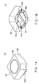
- FIGS. 1A and 1B are perspective views of the surface mount inductor of the present invention.
- FIG. 1A shows a perspective view from above.
- FIG. 1B shows a perspective view from below.
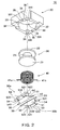
- FIG. 2 shows an exploded perspective view of the surface mount inductor shown in FIGS. 1A and 1B .
- a surface mount inductor 10 of the present invention includes: a drum core 20; a coil 40 including an insulation-coated lead wire wound around the drum core 20; a ring core 30 arranged on an outer periphery of the drum core 20 through a gap 60; and a pair of metal terminals 50a and 50b arranged on a bottom surface of the drum core 20.
- the drum core 20 includes a disc-shaped upper collar 22 and a lower collar 23 on opposite ends of a spool 21, and the coil 40 is wound around the spool 21.
- the ring core 30 has a substantially rectangular outer shape and includes, at a center, an insertion hole 31 having a diameter slightly larger than outside diameters of the collars 22 and 23 of the drum core 20.
- the ring core 30 includes: lower stage surfaces 32 and 32 formed by cutting out one of the pairs of opposing comers; and grooves 34 and 34 on the other pair of opposing corners, each of the grooves 34 including a stepped section 341 between a lower end surface 35 and the groove 34.
- upper stage surfaces 33 and 33 cut out lower than the lower stage surfaces 32 are provided, each of the upper stage surfaces 33 including a stepped section 331 between the lower end surface 35 and the upper stage surface 33.
- the ring core 30 includes a chamfered section 36 chamfered to indicate polarity of the surface mount inductor.
- the pair of metal terminals 50a and 50b are formed by punching a predetermined shape on a lead frame made of a continuous thin metal plate.
- Each of the metal terminals 50a and 50b includes: a bottom section 51 in a semicircular shape; tongues 52, 53, and 54 projecting in peripheral directions from over an arc of the bottom section 51; and connection sections 59 and 59 connected to the lead frame.
- the tongue 52 is bent upward like a crank to provide a stepped section 521.
- the tongue 53 is once bent downward like a crank to provide a mount section 533 that serves as a mount terminal.
- a tip of the tongue 53 is bent in an upper direction along a side surface of the ring core 30.
- the tongue 54 is bent upward like a crank to provide a stepped section 541.
- the metal terminals 50a and 50b are adhered and fixed to the bottom surface of the lower collar 23 so that the stepped sections 521 and 541 abut against the outer periphery of the lower collar 23 of the drum core 20.
- Terminal sections 41a and 41b of the coil 40 are tied up to the metal terminals 50a and 50b, respectively.
- the tie-up sections are immersed in a solder bath to remove the insulation coating, and the terminals sections 41a and 41b and the metal terminals 50a and 50b are separately and electrically connected.
- the ring core 30 is arranged on the outer periphery of the drum core 20, and an adhesive is injected to the gap 60 to adhere and fix the drum core 20 and the ring core 30.
- a side end surface 522 of the tongue 52 is abutting against the stepped section 341, and a side end surface 532 of the tongue 53 is abutting against the stepped section 331.
- the tongues 53 and 52 sandwich the lower end surface 35 from both sides.
- the tip of the tongue 52 is abutting against the groove 34, and the tip of the tongue 53 is abutting against the upper stage surface 33.
- the tongues 52 and 53 position the ring core 30 in a horizontal direction and position the bottom surface of the ring core 30. Positioning of the metal terminals 50a and 50b relative to the drum core 20 is relatively easy. Therefore, the structure of the surface mount inductor allows accurate positioning of the drum core and the ring core without using spacers, and the gap can be constant. As a result, a surface mount inductor with stable characteristics can be inexpensively provided.
- solder fillets formed between the sidewall and a pad on a printed circuit board can be easily observed.
- the solder fillets are formed when the surface mount inductor 10 is mounted on a printed circuit board.
- the tongues 52 abut against the drum core 20 at the stepped section 521, and the side end surfaces 522 abut against the ring core 30 in the embodiment.
- the tongues may be divided into tongues abutting against the drum core 20 and tongues abutting against the ring core 30.
- the terminal section of the coil may be tied up to the tip section of the tongue 53.
- connection sections may also be used as tongues.
Landscapes
- Engineering & Computer Science (AREA)
- Power Engineering (AREA)
- Microelectronics & Electronic Packaging (AREA)
- Coils Or Transformers For Communication (AREA)
Description
- The present invention relates to a low profile surface mount inductor including a ring core arranged on an outer periphery of a drum core, the ring core surrounding the drum core.
- An inductor including a coil wound around a drum core and including a ring core arranged on an outer periphery of the drum core is used for a choke coil of a DC/DC converter or the like. Along with the reduction in the size and thickness of electronic devices, reduction in the height of the inductor is also demanded. Recently, a low profile inductor including metal terminals directly adhered to a bottom surface of a drum core has been in use (
Japanese Patent Laid-Open Nos. 2009-176954 2005-340607 - Japanese Patent Application
JP 2003-217942 A - In general, an inductor formed by combining a drum core and a ring core is provided with a gap at a predetermined spacing between the drum core and the ring core to adjust electrical characteristics, such as inductance characteristics and a superimposed direct current value.
- The electrical characteristics of the inductor are changed by adjusting the spacing of the gap. The spacing of the gap is about 0.1 mm to 0.50 mm, and this is significantly small. Therefore, variations in the assembly cause variations in the electrical characteristics of the inductor.
- The spacing of the gap needs to be constant to reduce the variations in the electrical characteristics of the inductor.
-
FIGS. 3A to 3D are schematic plan views illustrating examples of the gap between the drum core and the ring core of the inductor formed by combining the drum core and the ring core.FIG. 3A shows a normal gap of the inductor.FIG. 3B shows a case where the position of the drum core is decentered.FIG. 3C shows a case where the spacing of the gap is enlarged.FIG. 3D shows a case where spacers are inserted to the gap. - As shown in
FIG. 3A , adrum core 2 and aring core 3 are arranged in the normal inductor so that a spacing do of agap 6 between thedrum core 2 and thering core 3 is uniform throughout the entire circumference. - Meanwhile, the
drum core 2 is decentered, and part of thedrum core 2 and thering core 3 comes into contact in the inductor shown inFIG. 3B . Although an initial inductance value is greater than that of the inductor shown inFIG. 3A , the inductance value rapidly decreases with an increase in a direct current. This reduces a maximum superimposed direct current. -
FIG. 3C shows a case where the spacing of thegap 6 is enlarged to prevent thedrum core 2 and thering core 3 from coming into contact with each other even if there is some mislocation. If a spacing d1 of thegap 6 is enlarged as inFIG. 3C (do < d1), the initial inductance value is reduced, and the number of windings needs to be increased. This poses a problem that direct current resistance increases. - Consequently,
spacers 7 can be inserted to thegap 6 as shown inFIG. 3D . Thespacers 7 may be temporarily used in the assembly or may be incorporated into the inductor. - However, the thickness of the
spacers 7 needs to be reduced to 0.01 mm to 0.40 mm when thespacers 7 are used only in the assembly. There is a problem in the durability of thespacers 7, and there is a problem that the manufacturing cost increases. - There is a problem of an increase in the material cost when the
spacers 7 are incorporated into the inductor. Metal terminals can also function as spacers. However, a magnetic flux penetrates through the metallic spacers, and an eddy current loss occurs at the metal terminals. There is a problem that the characteristics of the inductor are reduced. - To solve the problems, the present invention provides a surface mount inductor according to appended claim 1.
- According to the surface mount inductor of the present invention, the drum core and the ring core can be positioned without enlarging the spacing of the gap and without using the spacers. As a result, a surface mount inductor with stable electrical characteristics can be inexpensively provided.
-
-
FIGS. 1A and 1B are perspective views of a surface mount inductor of the present invention; -
FIG. 2 is an exploded perspective view ofFIG. 1 ; and -
FIGS. 3A to 3D are schematic plan views for describing gaps of conventional surface mount inductors. - An embodiment of a surface mount inductor of the present invention will now be described with reference to
FIGS. 1A, 1B and2 .FIGS. 1A and 1B are perspective views of the surface mount inductor of the present invention.FIG. 1A shows a perspective view from above.FIG. 1B shows a perspective view from below.FIG. 2 shows an exploded perspective view of the surface mount inductor shown inFIGS. 1A and 1B . - As shown in
FIGS. 1A, 1B , and2 , asurface mount inductor 10 of the present invention includes: adrum core 20; acoil 40 including an insulation-coated lead wire wound around thedrum core 20; aring core 30 arranged on an outer periphery of thedrum core 20 through agap 60; and a pair ofmetal terminals drum core 20. - The
drum core 20 includes a disc-shapedupper collar 22 and alower collar 23 on opposite ends of aspool 21, and thecoil 40 is wound around thespool 21. - The
ring core 30 has a substantially rectangular outer shape and includes, at a center, aninsertion hole 31 having a diameter slightly larger than outside diameters of thecollars drum core 20. On a bottom surface, thering core 30 includes: lower stage surfaces 32 and 32 formed by cutting out one of the pairs of opposing comers; andgrooves grooves 34 including a steppedsection 341 between alower end surface 35 and thegroove 34. On one of the pairs of opposing sides adjacent to the lower stage surfaces 32, upper stage surfaces 33 and 33 cut out lower than the lower stage surfaces 32 are provided, each of the upper stage surfaces 33 including a steppedsection 331 between thelower end surface 35 and theupper stage surface 33. - As a result, convex sections are formed by the stepped
sections lower end surface 35. On one corner, thering core 30 includes a chamferedsection 36 chamfered to indicate polarity of the surface mount inductor. - The pair of
metal terminals metal terminals bottom section 51 in a semicircular shape;tongues bottom section 51; andconnection sections - The
tongue 52 is bent upward like a crank to provide a steppedsection 521. Thetongue 53 is once bent downward like a crank to provide amount section 533 that serves as a mount terminal. A tip of thetongue 53 is bent in an upper direction along a side surface of thering core 30. Thetongue 54 is bent upward like a crank to provide a steppedsection 541. - In the assembly of the
surface mount inductor 10, themetal terminals lower collar 23 so that the steppedsections lower collar 23 of thedrum core 20. -
Terminal sections coil 40 are tied up to themetal terminals terminals sections metal terminals - The
ring core 30 is arranged on the outer periphery of thedrum core 20, and an adhesive is injected to thegap 60 to adhere and fix thedrum core 20 and thering core 30. - In this case, a
side end surface 522 of thetongue 52 is abutting against the steppedsection 341, and aside end surface 532 of thetongue 53 is abutting against the steppedsection 331. In this way, thetongues lower end surface 35 from both sides. The tip of thetongue 52 is abutting against thegroove 34, and the tip of thetongue 53 is abutting against theupper stage surface 33. - In the
surface mount inductor 10, thetongues ring core 30 in a horizontal direction and position the bottom surface of thering core 30. Positioning of themetal terminals drum core 20 is relatively easy. Therefore, the structure of the surface mount inductor allows accurate positioning of the drum core and the ring core without using spacers, and the gap can be constant. As a result, a surface mount inductor with stable characteristics can be inexpensively provided. - Since the tip of the
tongue 53 is bent along the sidewall of thering core 30, solder fillets formed between the sidewall and a pad on a printed circuit board can be easily observed. The solder fillets are formed when thesurface mount inductor 10 is mounted on a printed circuit board. - Although an embodiment of the present invention has been described with reference to the drawings, the present invention is not limited to this.
- For example, the
tongues 52 abut against thedrum core 20 at the steppedsection 521, and the side end surfaces 522 abut against thering core 30 in the embodiment. However, the tongues may be divided into tongues abutting against thedrum core 20 and tongues abutting against thering core 30. Furthermore, the terminal section of the coil may be tied up to the tip section of thetongue 53. - More specifically, only at least two tongues that sandwich the convex section from both sides and at least two tongues that support the drum core from below are required. The connection sections may also be used as tongues.
Claims (4)
- A surface mount inductor comprising:a drum core (20) comprising a spool (21) provided with collars (22, 23), the collars comprising an upper collar (22) and a lower collar (23) provided on opposite ends of the spool (21);a coil (40) wound around the spool (21);a pair of metal terminals (50a, 50b) adhered to a lower surface of the lower collar (23); anda ring core (30) arranged on an outer periphery of the drum core (20), whereineach of the metal terminals (50a, 50b) comprises a plurality of tongues (52, 53, 54) projecting outwardly in different peripheral directions of the lower collar (23),at least two of the plurality of tongues (52, 53, 54) respectively comprise side end surfaces (522, 532);and wherein the at least two of the plurality of tongues (52, 53, 54) abut against the lower end surface (35) of the ring core (30),the surface mount inductor characterised in that:the ring core (30) is provided with projected portions formed by stepped sections (331, 341) which form lower end surfaces (35) therebetween;at least two of the plurality of tongues (52, 53, 54) respectively further comprise stepped sections (521, 541) abutting against an outer edge of the lower collar (23) of the drum core (20); andthe at least two of the plurality of tongues (52, 53, 54) provided on the metal terminals (50a, 50b) sandwich the projected portions between the respective side end surfaces (522, 532) of the adjacent pair of tongues.
- The surface mount inductor according to claim 1, wherein
a terminal section (41a, 41b) of the coil is tied up to one of the plurality of tongues (52, 53, 54). - The surface mount inductor according to claim 2, wherein
the plurality of tongues (52, 53, 54) are arranged below an upper surface of the lower collar (23). - The surface mount inductor according to claim 3, wherein
projected portions projecting below the lower collar (23) are arranged on the plurality of tongues (52, 53, 54), and the projected portions serve as mount terminals.
Applications Claiming Priority (1)
| Application Number | Priority Date | Filing Date | Title |
|---|---|---|---|
| JP2012114195A JP2013243192A (en) | 2012-05-18 | 2012-05-18 | Surface mounting inductor |
Publications (2)
| Publication Number | Publication Date |
|---|---|
| EP2665070A1 EP2665070A1 (en) | 2013-11-20 |
| EP2665070B1 true EP2665070B1 (en) | 2016-06-22 |
Family
ID=48430533
Family Applications (1)
| Application Number | Title | Priority Date | Filing Date |
|---|---|---|---|
| EP13167805.4A Active EP2665070B1 (en) | 2012-05-18 | 2013-05-15 | Surface mount inductor |
Country Status (4)
| Country | Link |
|---|---|
| US (1) | US20130307657A1 (en) |
| EP (1) | EP2665070B1 (en) |
| JP (1) | JP2013243192A (en) |
| CN (1) | CN103426612B (en) |
Families Citing this family (8)
| Publication number | Priority date | Publication date | Assignee | Title |
|---|---|---|---|---|
| DE102014105370B4 (en) * | 2014-04-15 | 2026-08-06 | Tdk Electronics Ag | core component |
| CN104008850A (en) * | 2014-05-04 | 2014-08-27 | 太尼电电子科技(东莞)有限公司 | Square closed magnetic circuit chip inductor |
| JP6332073B2 (en) * | 2015-02-13 | 2018-05-30 | 株式会社村田製作所 | Coil parts |
| JP6577918B2 (en) * | 2016-08-02 | 2019-09-18 | 太陽誘電株式会社 | Coil parts |
| US10340074B2 (en) | 2016-12-02 | 2019-07-02 | Cyntec Co., Ltd. | Transformer |
| KR101803096B1 (en) * | 2017-10-18 | 2017-11-29 | (주)동안전자 | A shield type inductor |
| JP7390900B2 (en) * | 2020-01-16 | 2023-12-04 | Tdk株式会社 | coil device |
| CN120913991A (en) * | 2024-05-06 | 2025-11-07 | 台达电子企业管理(上海)有限公司 | Magnetic element and manufacturing method thereof |
Family Cites Families (24)
| Publication number | Priority date | Publication date | Assignee | Title |
|---|---|---|---|---|
| JPS5222523U (en) * | 1975-08-06 | 1977-02-17 | ||
| JPH09171929A (en) * | 1995-12-21 | 1997-06-30 | Matsushita Electric Ind Co Ltd | Small choke coil |
| JP3201958B2 (en) * | 1996-06-28 | 2001-08-27 | 太陽誘電株式会社 | Surface mount inductor |
| US6292083B1 (en) * | 1998-03-27 | 2001-09-18 | Taiyo Yuden Co., Ltd. | Surface-mount coil |
| JPH11283847A (en) * | 1998-03-31 | 1999-10-15 | Taiyo Yuden Co Ltd | Surface mount type coil |
| JP3655517B2 (en) * | 1999-12-09 | 2005-06-02 | 東京コイルエンジニアリング株式会社 | Pot rivet type core surface mount choke coil |
| JP3693557B2 (en) * | 2000-05-29 | 2005-09-07 | 松下電器産業株式会社 | Inductance element |
| JP3659207B2 (en) * | 2001-09-28 | 2005-06-15 | 松下電器産業株式会社 | Inductance element |
| JP4259020B2 (en) * | 2002-01-28 | 2009-04-30 | ミツミ電機株式会社 | Inductance element and manufacturing method thereof |
| JP4315425B2 (en) * | 2003-07-23 | 2009-08-19 | スミダコーポレーション株式会社 | Ultra-small surface mount coil device |
| JP4664006B2 (en) | 2004-05-28 | 2011-04-06 | スミダコーポレーション株式会社 | Inductor |
| JP4727325B2 (en) * | 2004-10-04 | 2011-07-20 | スミダコーポレーション株式会社 | Surface mount type coil |
| JP4513586B2 (en) * | 2005-01-31 | 2010-07-28 | Tdk株式会社 | Coil parts |
| JP4702601B2 (en) * | 2005-03-29 | 2011-06-15 | Tdk株式会社 | Coil parts |
| JP4676822B2 (en) * | 2005-06-21 | 2011-04-27 | スミダコーポレーション株式会社 | Coil parts |
| JP2007027461A (en) * | 2005-07-19 | 2007-02-01 | Sumida Corporation | Core and inductor with core |
| JP2007258194A (en) * | 2006-03-20 | 2007-10-04 | Sumida Corporation | Inductor |
| JP4838621B2 (en) * | 2006-04-12 | 2011-12-14 | スミダコーポレーション株式会社 | Transformer manufacturing method |
| JP5309682B2 (en) * | 2007-05-25 | 2013-10-09 | スミダコーポレーション株式会社 | Inductance element |
| CN101325122B (en) * | 2007-06-15 | 2013-06-26 | 库帕技术公司 | Miniature Shielded Magnetics |
| US8325000B2 (en) * | 2007-09-10 | 2012-12-04 | Sumida Corporation | Magnetic component |
| JP5154960B2 (en) | 2008-01-24 | 2013-02-27 | スミダコーポレーション株式会社 | Magnetic element and manufacturing method thereof |
| JP5232265B2 (en) * | 2010-05-31 | 2013-07-10 | 株式会社Maruwa | Inductor and manufacturing method thereof |
| JP3171315U (en) * | 2011-07-25 | 2011-10-27 | スミダコーポレーション株式会社 | Magnetic element |
-
2012
- 2012-05-18 JP JP2012114195A patent/JP2013243192A/en active Pending
-
2013
- 2013-05-08 US US13/889,413 patent/US20130307657A1/en not_active Abandoned
- 2013-05-15 EP EP13167805.4A patent/EP2665070B1/en active Active
- 2013-05-16 CN CN201310181480.1A patent/CN103426612B/en active Active
Also Published As
| Publication number | Publication date |
|---|---|
| US20130307657A1 (en) | 2013-11-21 |
| CN103426612B (en) | 2016-04-13 |
| CN103426612A (en) | 2013-12-04 |
| EP2665070A1 (en) | 2013-11-20 |
| JP2013243192A (en) | 2013-12-05 |
Similar Documents
| Publication | Publication Date | Title |
|---|---|---|
| EP2665070A1 (en) | Surface mount inductor | |
| US20130113591A1 (en) | Magnetic electrical device | |
| JP4781223B2 (en) | Inductance element | |
| US8203407B2 (en) | Surface mount magnetic device | |
| US9299491B2 (en) | Transformer coil | |
| CN103632819B (en) | Magnetic element | |
| KR20120014563A (en) | Surface-Mount Magnetic Components and Manufacturing Method Thereof | |
| EP2455952B1 (en) | Magnetic element | |
| WO2013148644A1 (en) | Flat coil planar transformer and methods | |
| JP2009252787A (en) | Coil component | |
| JP2018010999A (en) | Coil component | |
| JP4490698B2 (en) | Chip coil | |
| JP2020047862A (en) | Coil device and pulse transformer | |
| CN1933051B (en) | Inductor | |
| JP2003068531A (en) | Inductor and method of manufacturing inductor | |
| JP2007080922A5 (en) | ||
| CN111724979A (en) | Coil component and electronic device | |
| JP5247083B2 (en) | Magnetic element | |
| KR102558332B1 (en) | Inductor and producing method of the same | |
| JP2010153460A (en) | Coil component | |
| JP5154960B2 (en) | Magnetic element and manufacturing method thereof | |
| TWI447759B (en) | Surface mount magnetic component assembly | |
| JP5059050B2 (en) | Winding frame and winding parts | |
| JP4371958B2 (en) | Coil device | |
| JP2005285901A (en) | Electronic component and manufacturing method thereof |
Legal Events
| Date | Code | Title | Description |
|---|---|---|---|
| PUAI | Public reference made under article 153(3) epc to a published international application that has entered the european phase |
Free format text: ORIGINAL CODE: 0009012 |
|
| AK | Designated contracting states |
Kind code of ref document: A1 Designated state(s): AL AT BE BG CH CY CZ DE DK EE ES FI FR GB GR HR HU IE IS IT LI LT LU LV MC MK MT NL NO PL PT RO RS SE SI SK SM TR |
|
| AX | Request for extension of the european patent |
Extension state: BA ME |
|
| 17P | Request for examination filed |
Effective date: 20140404 |
|
| RBV | Designated contracting states (corrected) |
Designated state(s): AL AT BE BG CH CY CZ DE DK EE ES FI FR GB GR HR HU IE IS IT LI LT LU LV MC MK MT NL NO PL PT RO RS SE SI SK SM TR |
|
| 17Q | First examination report despatched |
Effective date: 20140513 |
|
| GRAP | Despatch of communication of intention to grant a patent |
Free format text: ORIGINAL CODE: EPIDOSNIGR1 |
|
| INTG | Intention to grant announced |
Effective date: 20151208 |
|
| GRAS | Grant fee paid |
Free format text: ORIGINAL CODE: EPIDOSNIGR3 |
|
| GRAA | (expected) grant |
Free format text: ORIGINAL CODE: 0009210 |
|
| AK | Designated contracting states |
Kind code of ref document: B1 Designated state(s): AL AT BE BG CH CY CZ DE DK EE ES FI FR GB GR HR HU IE IS IT LI LT LU LV MC MK MT NL NO PL PT RO RS SE SI SK SM TR |
|
| REG | Reference to a national code |
Ref country code: GB Ref legal event code: FG4D |
|
| REG | Reference to a national code |
Ref country code: CH Ref legal event code: EP |
|
| REG | Reference to a national code |
Ref country code: IE Ref legal event code: FG4D |
|
| REG | Reference to a national code |
Ref country code: AT Ref legal event code: REF Ref document number: 808089 Country of ref document: AT Kind code of ref document: T Effective date: 20160715 |
|
| REG | Reference to a national code |
Ref country code: DE Ref legal event code: R096 Ref document number: 602013008702 Country of ref document: DE |
|
| REG | Reference to a national code |
Ref country code: LT Ref legal event code: MG4D |
|
| REG | Reference to a national code |
Ref country code: NL Ref legal event code: MP Effective date: 20160622 |
|
| PG25 | Lapsed in a contracting state [announced via postgrant information from national office to epo] |
Ref country code: FI Free format text: LAPSE BECAUSE OF FAILURE TO SUBMIT A TRANSLATION OF THE DESCRIPTION OR TO PAY THE FEE WITHIN THE PRESCRIBED TIME-LIMIT Effective date: 20160622 Ref country code: LT Free format text: LAPSE BECAUSE OF FAILURE TO SUBMIT A TRANSLATION OF THE DESCRIPTION OR TO PAY THE FEE WITHIN THE PRESCRIBED TIME-LIMIT Effective date: 20160622 Ref country code: NO Free format text: LAPSE BECAUSE OF FAILURE TO SUBMIT A TRANSLATION OF THE DESCRIPTION OR TO PAY THE FEE WITHIN THE PRESCRIBED TIME-LIMIT Effective date: 20160922 |
|
| REG | Reference to a national code |
Ref country code: AT Ref legal event code: MK05 Ref document number: 808089 Country of ref document: AT Kind code of ref document: T Effective date: 20160622 |
|
| PG25 | Lapsed in a contracting state [announced via postgrant information from national office to epo] |
Ref country code: NL Free format text: LAPSE BECAUSE OF FAILURE TO SUBMIT A TRANSLATION OF THE DESCRIPTION OR TO PAY THE FEE WITHIN THE PRESCRIBED TIME-LIMIT Effective date: 20160622 Ref country code: SE Free format text: LAPSE BECAUSE OF FAILURE TO SUBMIT A TRANSLATION OF THE DESCRIPTION OR TO PAY THE FEE WITHIN THE PRESCRIBED TIME-LIMIT Effective date: 20160622 Ref country code: RS Free format text: LAPSE BECAUSE OF FAILURE TO SUBMIT A TRANSLATION OF THE DESCRIPTION OR TO PAY THE FEE WITHIN THE PRESCRIBED TIME-LIMIT Effective date: 20160622 Ref country code: GR Free format text: LAPSE BECAUSE OF FAILURE TO SUBMIT A TRANSLATION OF THE DESCRIPTION OR TO PAY THE FEE WITHIN THE PRESCRIBED TIME-LIMIT Effective date: 20160923 Ref country code: HR Free format text: LAPSE BECAUSE OF FAILURE TO SUBMIT A TRANSLATION OF THE DESCRIPTION OR TO PAY THE FEE WITHIN THE PRESCRIBED TIME-LIMIT Effective date: 20160622 Ref country code: LV Free format text: LAPSE BECAUSE OF FAILURE TO SUBMIT A TRANSLATION OF THE DESCRIPTION OR TO PAY THE FEE WITHIN THE PRESCRIBED TIME-LIMIT Effective date: 20160622 |
|
| PG25 | Lapsed in a contracting state [announced via postgrant information from national office to epo] |
Ref country code: CZ Free format text: LAPSE BECAUSE OF FAILURE TO SUBMIT A TRANSLATION OF THE DESCRIPTION OR TO PAY THE FEE WITHIN THE PRESCRIBED TIME-LIMIT Effective date: 20160622 Ref country code: SK Free format text: LAPSE BECAUSE OF FAILURE TO SUBMIT A TRANSLATION OF THE DESCRIPTION OR TO PAY THE FEE WITHIN THE PRESCRIBED TIME-LIMIT Effective date: 20160622 Ref country code: IT Free format text: LAPSE BECAUSE OF FAILURE TO SUBMIT A TRANSLATION OF THE DESCRIPTION OR TO PAY THE FEE WITHIN THE PRESCRIBED TIME-LIMIT Effective date: 20160622 Ref country code: IS Free format text: LAPSE BECAUSE OF FAILURE TO SUBMIT A TRANSLATION OF THE DESCRIPTION OR TO PAY THE FEE WITHIN THE PRESCRIBED TIME-LIMIT Effective date: 20161022 Ref country code: RO Free format text: LAPSE BECAUSE OF FAILURE TO SUBMIT A TRANSLATION OF THE DESCRIPTION OR TO PAY THE FEE WITHIN THE PRESCRIBED TIME-LIMIT Effective date: 20160622 Ref country code: EE Free format text: LAPSE BECAUSE OF FAILURE TO SUBMIT A TRANSLATION OF THE DESCRIPTION OR TO PAY THE FEE WITHIN THE PRESCRIBED TIME-LIMIT Effective date: 20160622 |
|
| PG25 | Lapsed in a contracting state [announced via postgrant information from national office to epo] |
Ref country code: AT Free format text: LAPSE BECAUSE OF FAILURE TO SUBMIT A TRANSLATION OF THE DESCRIPTION OR TO PAY THE FEE WITHIN THE PRESCRIBED TIME-LIMIT Effective date: 20160622 Ref country code: PL Free format text: LAPSE BECAUSE OF FAILURE TO SUBMIT A TRANSLATION OF THE DESCRIPTION OR TO PAY THE FEE WITHIN THE PRESCRIBED TIME-LIMIT Effective date: 20160622 Ref country code: SM Free format text: LAPSE BECAUSE OF FAILURE TO SUBMIT A TRANSLATION OF THE DESCRIPTION OR TO PAY THE FEE WITHIN THE PRESCRIBED TIME-LIMIT Effective date: 20160622 Ref country code: BE Free format text: LAPSE BECAUSE OF FAILURE TO SUBMIT A TRANSLATION OF THE DESCRIPTION OR TO PAY THE FEE WITHIN THE PRESCRIBED TIME-LIMIT Effective date: 20160622 Ref country code: ES Free format text: LAPSE BECAUSE OF FAILURE TO SUBMIT A TRANSLATION OF THE DESCRIPTION OR TO PAY THE FEE WITHIN THE PRESCRIBED TIME-LIMIT Effective date: 20160622 Ref country code: PT Free format text: LAPSE BECAUSE OF FAILURE TO SUBMIT A TRANSLATION OF THE DESCRIPTION OR TO PAY THE FEE WITHIN THE PRESCRIBED TIME-LIMIT Effective date: 20161024 |
|
| REG | Reference to a national code |
Ref country code: DE Ref legal event code: R097 Ref document number: 602013008702 Country of ref document: DE |
|
| PLBE | No opposition filed within time limit |
Free format text: ORIGINAL CODE: 0009261 |
|
| STAA | Information on the status of an ep patent application or granted ep patent |
Free format text: STATUS: NO OPPOSITION FILED WITHIN TIME LIMIT |
|
| REG | Reference to a national code |
Ref country code: FR Ref legal event code: PLFP Year of fee payment: 5 |
|
| 26N | No opposition filed |
Effective date: 20170323 |
|
| PG25 | Lapsed in a contracting state [announced via postgrant information from national office to epo] |
Ref country code: DK Free format text: LAPSE BECAUSE OF FAILURE TO SUBMIT A TRANSLATION OF THE DESCRIPTION OR TO PAY THE FEE WITHIN THE PRESCRIBED TIME-LIMIT Effective date: 20160622 |
|
| REG | Reference to a national code |
Ref country code: DE Ref legal event code: R082 Ref document number: 602013008702 Country of ref document: DE Representative=s name: DENNEMEYER & ASSOCIATES S.A., DE Ref country code: DE Ref legal event code: R081 Ref document number: 602013008702 Country of ref document: DE Owner name: MURATA MANUFACTURING CO., LTD., NAGAOKAKYO-SHI, JP Free format text: FORMER OWNER: TOKO, INC, TSURUGASHIMA-SHI, SAITAMA, KE |
|
| PG25 | Lapsed in a contracting state [announced via postgrant information from national office to epo] |
Ref country code: LU Free format text: LAPSE BECAUSE OF NON-PAYMENT OF DUE FEES Effective date: 20170531 Ref country code: SI Free format text: LAPSE BECAUSE OF FAILURE TO SUBMIT A TRANSLATION OF THE DESCRIPTION OR TO PAY THE FEE WITHIN THE PRESCRIBED TIME-LIMIT Effective date: 20160622 |
|
| REG | Reference to a national code |
Ref country code: CH Ref legal event code: PL |
|
| PG25 | Lapsed in a contracting state [announced via postgrant information from national office to epo] |
Ref country code: MC Free format text: LAPSE BECAUSE OF FAILURE TO SUBMIT A TRANSLATION OF THE DESCRIPTION OR TO PAY THE FEE WITHIN THE PRESCRIBED TIME-LIMIT Effective date: 20160622 |
|
| REG | Reference to a national code |
Ref country code: IE Ref legal event code: MM4A |
|
| REG | Reference to a national code |
Ref country code: FR Ref legal event code: TP Owner name: MURATA MANUFACTURING CO., LTD., JP Effective date: 20180124 |
|
| PG25 | Lapsed in a contracting state [announced via postgrant information from national office to epo] |
Ref country code: LI Free format text: LAPSE BECAUSE OF NON-PAYMENT OF DUE FEES Effective date: 20170531 Ref country code: CH Free format text: LAPSE BECAUSE OF NON-PAYMENT OF DUE FEES Effective date: 20170531 |
|
| REG | Reference to a national code |
Ref country code: GB Ref legal event code: 732E Free format text: REGISTERED BETWEEN 20180208 AND 20180214 |
|
| PG25 | Lapsed in a contracting state [announced via postgrant information from national office to epo] |
Ref country code: LU Free format text: LAPSE BECAUSE OF NON-PAYMENT OF DUE FEES Effective date: 20170515 |
|
| PG25 | Lapsed in a contracting state [announced via postgrant information from national office to epo] |
Ref country code: IE Free format text: LAPSE BECAUSE OF NON-PAYMENT OF DUE FEES Effective date: 20170515 |
|
| REG | Reference to a national code |
Ref country code: FR Ref legal event code: PLFP Year of fee payment: 6 |
|
| PG25 | Lapsed in a contracting state [announced via postgrant information from national office to epo] |
Ref country code: MT Free format text: LAPSE BECAUSE OF NON-PAYMENT OF DUE FEES Effective date: 20170515 |
|
| PG25 | Lapsed in a contracting state [announced via postgrant information from national office to epo] |
Ref country code: AL Free format text: LAPSE BECAUSE OF FAILURE TO SUBMIT A TRANSLATION OF THE DESCRIPTION OR TO PAY THE FEE WITHIN THE PRESCRIBED TIME-LIMIT Effective date: 20160622 |
|
| PG25 | Lapsed in a contracting state [announced via postgrant information from national office to epo] |
Ref country code: HU Free format text: LAPSE BECAUSE OF FAILURE TO SUBMIT A TRANSLATION OF THE DESCRIPTION OR TO PAY THE FEE WITHIN THE PRESCRIBED TIME-LIMIT; INVALID AB INITIO Effective date: 20130515 |
|
| PG25 | Lapsed in a contracting state [announced via postgrant information from national office to epo] |
Ref country code: BG Free format text: LAPSE BECAUSE OF FAILURE TO SUBMIT A TRANSLATION OF THE DESCRIPTION OR TO PAY THE FEE WITHIN THE PRESCRIBED TIME-LIMIT Effective date: 20160622 |
|
| PG25 | Lapsed in a contracting state [announced via postgrant information from national office to epo] |
Ref country code: CY Free format text: LAPSE BECAUSE OF NON-PAYMENT OF DUE FEES Effective date: 20160622 |
|
| PG25 | Lapsed in a contracting state [announced via postgrant information from national office to epo] |
Ref country code: MK Free format text: LAPSE BECAUSE OF FAILURE TO SUBMIT A TRANSLATION OF THE DESCRIPTION OR TO PAY THE FEE WITHIN THE PRESCRIBED TIME-LIMIT Effective date: 20160622 |
|
| PG25 | Lapsed in a contracting state [announced via postgrant information from national office to epo] |
Ref country code: TR Free format text: LAPSE BECAUSE OF FAILURE TO SUBMIT A TRANSLATION OF THE DESCRIPTION OR TO PAY THE FEE WITHIN THE PRESCRIBED TIME-LIMIT Effective date: 20160622 |
|
| REG | Reference to a national code |
Ref country code: DE Ref legal event code: R082 Ref document number: 602013008702 Country of ref document: DE Representative=s name: DENNEMEYER & ASSOCIATES RECHTSANWALTSGESELLSCH, DE |
|
| PGFP | Annual fee paid to national office [announced via postgrant information from national office to epo] |
Ref country code: GB Payment date: 20260522 Year of fee payment: 14 |
|
| PGFP | Annual fee paid to national office [announced via postgrant information from national office to epo] |
Ref country code: DE Payment date: 20260522 Year of fee payment: 14 |
|
| PGFP | Annual fee paid to national office [announced via postgrant information from national office to epo] |
Ref country code: FR Payment date: 20260526 Year of fee payment: 14 |