EP2662473A1 - Conductive member - Google Patents
Conductive member Download PDFInfo
- Publication number
- EP2662473A1 EP2662473A1 EP11854649.8A EP11854649A EP2662473A1 EP 2662473 A1 EP2662473 A1 EP 2662473A1 EP 11854649 A EP11854649 A EP 11854649A EP 2662473 A1 EP2662473 A1 EP 2662473A1
- Authority
- EP
- European Patent Office
- Prior art keywords
- conductive
- conductive member
- conductive material
- metal film
- member according
- Prior art date
- Legal status (The legal status is an assumption and is not a legal conclusion. Google has not performed a legal analysis and makes no representation as to the accuracy of the status listed.)
- Granted
Links
Images

Classifications
-
- H—ELECTRICITY
- H01—ELECTRIC ELEMENTS
- H01B—CABLES; CONDUCTORS; INSULATORS; SELECTION OF MATERIALS FOR THEIR CONDUCTIVE, INSULATING OR DIELECTRIC PROPERTIES
- H01B5/00—Non-insulated conductors or conductive bodies characterised by their form
- H01B5/02—Single bars, rods, wires, or strips
-
- C—CHEMISTRY; METALLURGY
- C23—COATING METALLIC MATERIAL; COATING MATERIAL WITH METALLIC MATERIAL; CHEMICAL SURFACE TREATMENT; DIFFUSION TREATMENT OF METALLIC MATERIAL; COATING BY VACUUM EVAPORATION, BY SPUTTERING, BY ION IMPLANTATION OR BY CHEMICAL VAPOUR DEPOSITION, IN GENERAL; INHIBITING CORROSION OF METALLIC MATERIAL OR INCRUSTATION IN GENERAL
- C23C—COATING METALLIC MATERIAL; COATING MATERIAL WITH METALLIC MATERIAL; SURFACE TREATMENT OF METALLIC MATERIAL BY DIFFUSION INTO THE SURFACE, BY CHEMICAL CONVERSION OR SUBSTITUTION; COATING BY VACUUM EVAPORATION, BY SPUTTERING, BY ION IMPLANTATION OR BY CHEMICAL VAPOUR DEPOSITION, IN GENERAL
- C23C24/00—Coating starting from inorganic powder
- C23C24/02—Coating starting from inorganic powder by application of pressure only
- C23C24/04—Impact or kinetic deposition of particles
-
- H—ELECTRICITY
- H01—ELECTRIC ELEMENTS
- H01B—CABLES; CONDUCTORS; INSULATORS; SELECTION OF MATERIALS FOR THEIR CONDUCTIVE, INSULATING OR DIELECTRIC PROPERTIES
- H01B1/00—Conductors or conductive bodies characterised by the conductive materials; Selection of materials as conductors
- H01B1/02—Conductors or conductive bodies characterised by the conductive materials; Selection of materials as conductors mainly consisting of metals or alloys
Definitions
- the present invention relates to a conductive member, which is used when an electrode, an electrical wire, and the like are electrically connected.
- a conductive member called a bus bar which is a metal disposed as a power transmission line and the like, has conventionally been used in power plants, electric systems of transportation machines such as a vehicle, home electric appliances, and the like.
- the bus bar is in an elongated flat plate shape or in a long and thin rod shape, and due to a large surface area thereof, it has high heat dissipation and superior conductivity for allowing a large current to be flowed therein.
- the thermal spraying method is a method of forming a film by spraying a thermal spraying material, which is heated to a molten or nearly-molten state, onto a substrate.
- the cold spraying method is a method of forming a film on a surface of the substrate by spraying powder of a material to be the film together with an inert gas, which is below a melting point or a softening point, from a convergent-divergent (Laval) nozzle.
- the material to be the film which is in a solid state, is collided with the substrate (see, for example, Patent Document 1).
- an influence of thermal stress is mitigated because a temperature used is low, no phase transformation occurs, and oxidization can be inhibited. Therefore, it is possible to obtain a metal film in which a decrease of electrical conductivity is restrained.
- both the substrate and the material to be the film are metal
- plastic deformation occurs between the powder and the substrate by the powder to be the film colliding with the substrate, whereby an anchor effect can be obtained.
- respective oxide films are destroyed when the powder collides with the substrate, and a metallic bond is formed between newly-formed surfaces, whereby an effect of obtaining a laminate having a high adhesive strength is also expected.
- Patent Literature 1 US Patent No. 5,302,414 Summary
- the present invention has been made in view of the above, and an object thereof is to provide a conductive member in which a plurality of conductive materials can be joined at a low cost regardless of the substrate thickness and which has a good electrical conductivity.
- a conductive member includes: a first and a second conductive materials, at least one of which contains a conductive material having electrical resistance lower than aluminum; and a metal film formed by depositing powder including a metal, which is accelerated together with a gas and sprayed, in a solid state, onto a surface of a butting part, where the first and the second conductive materials are butted against each other.
- each of the first and the second conductive materials includes a cutout portion having a cutout shape in an end on a butting side, and the metal film covers the cutout portion.
- the cutout portion has a tapered shape, which is inclined relative to each of principal surfaces of the first and the second conductive materials.
- the cutout portion has an angle of inclination from zero to 45 degrees relative to each of the principal surfaces of the first and the second conductive materials.
- the cutout portion has the angle of inclination from two to 35 degrees relative to each of the principal surfaces of the first and the second conductive materials.
- the metal included in the metal film includes at least one selected from a group consisting of copper, molybdenum, aluminum, tungsten, nickel, silver, and an alloy containing at least one of them.
- another one of the first and the second conductive materials is aluminum or an aluminum alloy.
- a conductive member according to the present invention is configured to join conductive materials by forming a film by a cold spraying method so as to cover at least a part of a contacting part of the conductive materials, which are in contact. Therefore, it has an effect that a plurality of conductive materials can be joined at a low cost regardless of a substrate thickness.
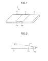
- FIG. 1 is a schematic perspective view illustrating a configuration of the conductive member according to the first embodiment.
- FIG. 2 is a schematic view illustrating a configuration of a principal part of the conductive member according to the first embodiment.
- a conductive member 1 illustrated in FIG. 1 is disposed as a power supply line and the like and includes a substantially plate-like first conductive material 11, which contains a lightweight and low-cost conductive material, a substantially plate-like second conductive material 12, which contains a conductive material having high electrical conductivity, and a metal film 13, which is formed between the first conductive material 11 and the second conductive material 12.
- the first conductive material 11 is substantially plate-like and includes a tapered portion 11a, which has a tapered shape at one of ends.
- the first conductive material 11 is formed of a lightweight and low cost material such as aluminum and an aluminum alloy.
- the second conductive material 12 is substantially plate-like and includes a tapered portion 12a, which is a cutout portion having a tapered shape at one of ends.
- the second conductive material 12 is formed of a material having the high electrical conductivity such as copper, a noble metal, a copper alloy and a noble metal alloy which have electrical resistance lower than aluminum.
- the tapered portion 11a includes an inclined plane 111, which is formed by cutting out one of faces of the first conductive material 11 and has a tapered shape, and an end face 112, which comes in contact with the second conductive material 12.
- an angle of inclination ⁇ 1 between the inclined plane 111 and a principal surface of the first conductive material 11 is in the range of zero to 45 degrees. More preferably, the angle of inclination ⁇ 1 is in the range of two to 35 degrees.
- a thickness d1 of the end face 112 be 0.1 to 0.5 times a maximum thickness of the first conductive material 11 after a tapered shape has been formed.
- the tapered portion 12a has the same angle of inclination and the same thickness as the above-described tapered portion 11a. Note that it is preferable that the angle of inclination and the thickness of the end face be the same between shapes of the tapered portion 11a and the tapered portion 12a.
- the metal film 13 is formed on a surface of the tapered portion 11a of the first conductive material 11 and a surface of the tapered portion 12a of the second conductive material 12 by the cold spraying method described below.
- a metal such as copper, molybdenum, aluminum, tungsten, nickel, silver, or the like, and an alloy containing at least one of these metals may be used.
- a metal or an alloy having density of 95% or more and thermal conductivity of 90% or more relative to a bulk material is applicable.
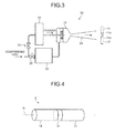
- FIG. 3 is a schematic view illustrating an outline of a cold spraying device used for forming the metal film 13.
- the forming of the metal film 13 by the cold spraying method is performed, for example, by using a cold spraying device 20 illustrated in FIG. 3 .
- the cold spraying device 20 includes a gas heater 21, which heats a compressed gas, a powder supply device 22, which houses a powdered material thermal-sprayed onto an object to be thermal-sprayed and supplies the powdered material to a spray gun 24, and a gas nozzle 23, which sprays material powder mixed with the compressed gas heated inside the spray gun 24 onto the tapered portions 11a and 12a of the first conductive member 11 and the second conductive material 12.
- Helium, nitrogen, air, or the like may be used as the compressed gas.
- the supplied compressed gas is supplied to the gas heater 21 and the powder supply device 22 through valves 25 and 26, respectively.
- the compressed gas supplied to the gas heater 21 is heated to, for example, between 50 and 700 degrees, and then it is supplied to the spray gun 24. More preferably, the compressed gas is heated so that an upper limit temperature of the powder, which is sprayed onto the tapered portions 11a and 12a, is kept to be not exceeding the melting point of the film material. By keeping the heating temperature of the powdered material to be not exceeding the melting point of the film material, it is possible to inhibit oxidization of the film material.
- the compressed gas supplied to the powder supply device 22 supplies the material powder having a particle diameter of about 10 to 100 ⁇ m, for example, inside the powder supply device 22 to the spray gun 24 in a predetermined discharge quantity.
- the heated compressed gas is made into a supersonic flow (about 340 m/s or above) by the gas nozzle 23, which has a convergent-divergent shape.
- the powdered material supplied to the spray gun 24 is accelerated by being put into this supersonic flow of the compressed gas and, while in the solid state, collides with forming faces of the tapered portions 11a and 12a at a high speed, whereby the film is formed.
- the metal film 13 as illustrated in FIG. 1 is formed.
- any device capable of forming the film by colliding the material powder in a solid state with the tapered portions 11a and 12a may be used, and it is not limited to the cold spraying device 20 illustrated in FIG. 3 .
- the conductive member according to the above-described first embodiment is configured to join two conductive materials by forming the metal film in the butting part thereof by the cold spraying method. Therefore, a plurality of conductive materials can be joined at a low cost regardless of the substrate thickness while also achieving good electrical conductivity. Furthermore, in the cold spraying method, compared to the welding, the thermal spraying method, or the like in which a high temperature is used in the processing, it is possible to form a fine metal film in which no phase transformation occurs, and oxidization is inhibited. Therefore, a metallic character of the metal film formed by the cold spraying method is better than a metallic character of the metal film formed by the thermal spraying method or the like. Accordingly, the electrical conductivity of the metal film is improved, and even more efficient electrical conductivity can be realized.
- the conductive member according to the first embodiment has no cutting process. Therefore, it is possible to manufacture the conductive member easily in a short time, improve a yield, and reduce the cost of manufacturing.
- the conductive materials are joined by forming the tapered portion having an inclined forming face in each of the conductive materials and by coating the tapered portion with the metal film, compared to a case where the conductive materials are joined only by butting without forming a tapered portion, a contact area between the conductive materials via the metal film is increased, whereby the electrical resistance can be decreased. Accordingly, the high electrical conductivity can be realized.
- the tapered portion has been described as a cutout shape having a plane, which is inclined relative to the principal surface of the conductive material; however, the forming face having the tapered shape may also be in an arc-like curved shape. Furthermore, the inclined plane of the tapered portion has been described as being formed on one of the faces of the conductive material; however, it can also be formed on both of the faces.
- FIG. 4 is a schematic perspective view illustrating a configuration of a conductive member according to the second embodiment.
- FIG. 5 is a schematic cross-sectional view illustrating a configuration of a principal part of the conductive member according to the second embodiment. Note that FIG. 5 is the cross-sectional view of a conductive member 2 illustrated in FIG. 4 , which is cut through a plane including a central axis N in a longitudinal direction.
- FIG. 6 is a schematic view illustrating a first conductive material 14. The conductive member 2 illustrated in FIG.
- first conductive material 14 which contains a lightweight and low cost conductive material
- substantially cylindrical second conductive material 15 which contains a conductive material having high electrical conductivity
- metal film 16 which is formed between the first conductive material 14 and the second conductive material 15.
- the first conductive material 14 is substantially plate-like and includes a tapered portion 14a, which has a tapered shape at one of ends.
- the first conductive material 14 is formed of a lightweight and low cost material such as aluminum and an aluminum alloy.
- the second conductive material 15 is substantially plate-like and includes a tapered portion 15a, which has a tapered shape at one of ends.
- the second conductive material 15 is formed of a material having high electrical conductivity such as copper, a noble metal, a copper alloy and a noble metal alloy.
- the metal film 16 is formed on surfaces of the tapered portion 14a of the first conductive material 14 and the tapered portion 15a of the second conductive material 15 by the cold spraying device 20 illustrated in FIG. 3 .
- the metal film 16 can be a metal such as copper, molybdenum, aluminum, tungsten, nickel, silver, or the like, and an alloy thereof.
- a metal or an alloy having density of 95% or more and thermal conductivity of 90% or more relative to a bulk material is applicable.
- the tapered portion 14a includes an inclined plane 141, which is formed by chamfering an end of the first conductive material 14 and has a tapered shape, and an end face 142, which comes in contact with the second conductive material 15.
- an angle of inclination ⁇ 2 between the inclined plane 141 of the tapered portion 14a and a principal surface of the first conductive material 14 is in the range of zero to 45 degrees as in the first embodiment. More preferably, the angle of inclination ⁇ 2 is in the range of two to 35 degrees.
- a diameter d2 of the end face 142 be 0.1 to 0.5 times the maximum diameter of the first conductive material 14 in a direction perpendicular to the central axis N after a tapered shape has been formed.
- the tapered portion 15a has the same angle of inclination and the same diameter of the end face as the above-described tapered portion 14a. Note that it is preferable that the angle of inclination and the diameter of the end face be the same between shapes of the tapered portion 14a and the tapered portion 15a.
- the conductive member according to the above-described second embodiment in the same way as the first embodiment, is configured to join two conductive materials by forming the metal film in the butting part thereof by the cold spraying method. Therefore, a plurality of conductive materials can be joined at a low cost regardless of the substrate thickness while achieving good electrical conductivity. Furthermore, in the cold spraying method, compared to the welding, the thermal spraying method, or the like in which a high temperature is used in the processing, it is possible to form a fine metal film in which no phase transformation occurs, and oxidization is inhibited. Therefore, a metallic character of the metal film formed by the cold spraying method is better than a metallic character of the metal film formed by the thermal spraying method or the like. Accordingly, the electrical conductivity of the metal film is improved, and even more efficient electrical conductivity can be realized.
- the base material is formed by forming a metal coating on the substrate by the cold spraying method and then by being cut into an intended thickness
- the conductive member according to the second embodiment has no cutting process. Therefore, it is possible to manufacture the conductive member easily in a short time, improve a yield, and reduce the cost of manufacturing.
- the conductive materials are joined by forming the tapered portion having an inclined forming face in each of the conductive materials and by coating the tapered portion with the metal film, compared to a case where the conductive materials are joined only by butting without forming a tapered portion, a contact area between the conductive materials via the metal film is increased, whereby the electrical resistance can be decreased. Accordingly, the high electrical conductivity can be realized.
- the conductive member according to the present invention is effective for manufacturing the conductive member by joining a plurality of conductive materials.
Landscapes
- Chemical & Material Sciences (AREA)
- Chemical Kinetics & Catalysis (AREA)
- Engineering & Computer Science (AREA)
- Materials Engineering (AREA)
- Mechanical Engineering (AREA)
- Metallurgy (AREA)
- Organic Chemistry (AREA)
- Other Surface Treatments For Metallic Materials (AREA)
- Coating By Spraying Or Casting (AREA)
- Non-Insulated Conductors (AREA)
Abstract
Description
- The present invention relates to a conductive member, which is used when an electrode, an electrical wire, and the like are electrically connected.
- A conductive member called a bus bar, which is a metal disposed as a power transmission line and the like, has conventionally been used in power plants, electric systems of transportation machines such as a vehicle, home electric appliances, and the like. The bus bar is in an elongated flat plate shape or in a long and thin rod shape, and due to a large surface area thereof, it has high heat dissipation and superior conductivity for allowing a large current to be flowed therein.
- In addition to the heat dissipation and the conductivity, weight saving and cost reduction are also sought after in the above-described bus bar. To meet such a demand, for example, there has been proposed a compound electrode combining aluminum, which is lightweight and low-cost, with copper, which has high electrical conductivity. Among methods for joining two metals in this compound electrode, there are welding, a thermal spraying method, and a cold spraying method. The thermal spraying method is a method of forming a film by spraying a thermal spraying material, which is heated to a molten or nearly-molten state, onto a substrate.
- The cold spraying method is a method of forming a film on a surface of the substrate by spraying powder of a material to be the film together with an inert gas, which is below a melting point or a softening point, from a convergent-divergent (Laval) nozzle. The material to be the film, which is in a solid state, is collided with the substrate (see, for example, Patent Document 1). In the cold spraying method, compared to the welding and the thermal spraying method, an influence of thermal stress is mitigated because a temperature used is low, no phase transformation occurs, and oxidization can be inhibited. Therefore, it is possible to obtain a metal film in which a decrease of electrical conductivity is restrained. In particular, in the case where both the substrate and the material to be the film are metal, plastic deformation occurs between the powder and the substrate by the powder to be the film colliding with the substrate, whereby an anchor effect can be obtained. Furthermore, in an area where the plastic deformation occurs, respective oxide films are destroyed when the powder collides with the substrate, and a metallic bond is formed between newly-formed surfaces, whereby an effect of obtaining a laminate having a high adhesive strength is also expected.
- Patent Literature 1:
US Patent No. 5,302,414 Summary - In the case of manufacturing a bus bar having a thin substrate, however, joining by the cold spraying method as disclosed in Patent Literature 1 raises a problem of an increased cost due to cutting work, because after a base material is manufactured by forming a metal film on the substrate, the base material needs to be cut into an intended substrate thickness.
- The present invention has been made in view of the above, and an object thereof is to provide a conductive member in which a plurality of conductive materials can be joined at a low cost regardless of the substrate thickness and which has a good electrical conductivity.
- To solve the problem described above and achieve the object, a conductive member according to the present invention includes: a first and a second conductive materials, at least one of which contains a conductive material having electrical resistance lower than aluminum; and a metal film formed by depositing powder including a metal, which is accelerated together with a gas and sprayed, in a solid state, onto a surface of a butting part, where the first and the second conductive materials are butted against each other.
- Moreover, in the conductive member described above, each of the first and the second conductive materials includes a cutout portion having a cutout shape in an end on a butting side, and the metal film covers the cutout portion.
- Moreover, in the conductive member described above, the cutout portion has a tapered shape, which is inclined relative to each of principal surfaces of the first and the second conductive materials.
- Moreover, in the conductive member described above, the cutout portion has an angle of inclination from zero to 45 degrees relative to each of the principal surfaces of the first and the second conductive materials.
- Moreover, in the conductive member described above, the cutout portion has the angle of inclination from two to 35 degrees relative to each of the principal surfaces of the first and the second conductive materials.
- Moreover, in the conductive member described above, the metal included in the metal film includes at least one selected from a group consisting of copper, molybdenum, aluminum, tungsten, nickel, silver, and an alloy containing at least one of them.
- Moreover, in the conductive member described above, another one of the first and the second conductive materials is aluminum or an aluminum alloy.
- A conductive member according to the present invention is configured to join conductive materials by forming a film by a cold spraying method so as to cover at least a part of a contacting part of the conductive materials, which are in contact. Therefore, it has an effect that a plurality of conductive materials can be joined at a low cost regardless of a substrate thickness. Brief Description of Drawings
-
-
FIG. 1 is a schematic perspective view illustrating a configuration of a conductive member according to a first embodiment of the present invention. -
FIG. 2 is a schematic view illustrating a configuration of a principal part of the conductive member according to the first embodiment of the present invention. -
FIG. 3 is a schematic view illustrating an outline of a cold spraying device used for manufacturing the conductive member according to the first embodiment of the present invention. -
FIG. 4 is a schematic perspective view illustrating a configuration of a conductive member according to a second embodiment of the present invention. -
FIG. 5 is a schematic cross-sectional view illustrating a configuration of a principal part of the conductive member according to the second embodiment of the present invention. -
FIG. 6 is a schematic view illustrating a configuration of a principal part of the conductive member according to the second embodiment of the present invention. Description of Embodiments - Embodiments for carrying out the present invention are described herein in detail with reference to the drawings. Note that the following embodiments are not intended to limit the present invention. Furthermore, each of the drawings referred to in the following descriptions is only a schematic illustration of a shape, a size, and a positional relationship to make a content of the present invention understandable. In other words, the present invention is not to be limited to the shape, the size, and the positional relationship exemplified in each of the drawings.
- First, a conductive member according to a first embodiment of the present invention is described herein in detail with reference to the drawings.
FIG. 1 is a schematic perspective view illustrating a configuration of the conductive member according to the first embodiment.FIG. 2 is a schematic view illustrating a configuration of a principal part of the conductive member according to the first embodiment. A conductive member 1 illustrated inFIG. 1 is disposed as a power supply line and the like and includes a substantially plate-like firstconductive material 11, which contains a lightweight and low-cost conductive material, a substantially plate-like secondconductive material 12, which contains a conductive material having high electrical conductivity, and ametal film 13, which is formed between the firstconductive material 11 and the secondconductive material 12. - The first
conductive material 11 is substantially plate-like and includes atapered portion 11a, which has a tapered shape at one of ends. The firstconductive material 11 is formed of a lightweight and low cost material such as aluminum and an aluminum alloy. - The second
conductive material 12 is substantially plate-like and includes atapered portion 12a, which is a cutout portion having a tapered shape at one of ends. The secondconductive material 12 is formed of a material having the high electrical conductivity such as copper, a noble metal, a copper alloy and a noble metal alloy which have electrical resistance lower than aluminum. - The
tapered portion 11a, as illustrated inFIG. 2 , includes aninclined plane 111, which is formed by cutting out one of faces of the firstconductive material 11 and has a tapered shape, and anend face 112, which comes in contact with the secondconductive material 12. Here, an angle of inclination θ1 between theinclined plane 111 and a principal surface of the firstconductive material 11 is in the range of zero to 45 degrees. More preferably, the angle of inclination θ1 is in the range of two to 35 degrees. Furthermore, in thetapered portion 11a, it is preferable that a thickness d1 of theend face 112 be 0.1 to 0.5 times a maximum thickness of the firstconductive material 11 after a tapered shape has been formed. - The
tapered portion 12a has the same angle of inclination and the same thickness as the above-describedtapered portion 11a. Note that it is preferable that the angle of inclination and the thickness of the end face be the same between shapes of thetapered portion 11a and thetapered portion 12a. - The
metal film 13 is formed on a surface of thetapered portion 11a of the firstconductive material 11 and a surface of thetapered portion 12a of the secondconductive material 12 by the cold spraying method described below. As the metal film 13 (film material), a metal such as copper, molybdenum, aluminum, tungsten, nickel, silver, or the like, and an alloy containing at least one of these metals may be used. Here, as themetal film 13, a metal or an alloy having density of 95% or more and thermal conductivity of 90% or more relative to a bulk material is applicable. - Note that in the first embodiment, it is preferable that a combination be used in which copper or a copper alloy is used as the first
conductive material 11, aluminum or an aluminum alloy is used as the secondconductive material 12, and copper or a copper alloy is used as themetal film 13. - Then, forming of the
metal film 13 is described with reference toFIG. 3. FIG. 3 is a schematic view illustrating an outline of a cold spraying device used for forming themetal film 13. The forming of themetal film 13 by the cold spraying method is performed, for example, by using acold spraying device 20 illustrated inFIG. 3 . - The
cold spraying device 20 includes agas heater 21, which heats a compressed gas, apowder supply device 22, which houses a powdered material thermal-sprayed onto an object to be thermal-sprayed and supplies the powdered material to aspray gun 24, and agas nozzle 23, which sprays material powder mixed with the compressed gas heated inside thespray gun 24 onto thetapered portions conductive member 11 and the secondconductive material 12. - Helium, nitrogen, air, or the like may be used as the compressed gas. The supplied compressed gas is supplied to the
gas heater 21 and thepowder supply device 22 throughvalves gas heater 21 is heated to, for example, between 50 and 700 degrees, and then it is supplied to thespray gun 24. More preferably, the compressed gas is heated so that an upper limit temperature of the powder, which is sprayed onto thetapered portions - The compressed gas supplied to the
powder supply device 22 supplies the material powder having a particle diameter of about 10 to 100 µm, for example, inside thepowder supply device 22 to thespray gun 24 in a predetermined discharge quantity. The heated compressed gas is made into a supersonic flow (about 340 m/s or above) by thegas nozzle 23, which has a convergent-divergent shape. The powdered material supplied to thespray gun 24 is accelerated by being put into this supersonic flow of the compressed gas and, while in the solid state, collides with forming faces of thetapered portions - By the above-described
cold spraying device 20, themetal film 13 as illustrated inFIG. 1 is formed. Note that any device capable of forming the film by colliding the material powder in a solid state with thetapered portions cold spraying device 20 illustrated inFIG. 3 . - In the above-described processing, it is possible to cover the surfaces of the tapered
portion 11a of the firstconductive material 11 and the taperedportion 12a of the secondconductive material 12 with themetal film 13. Note that in a case where there the surfaces of the firstconductive material 11 and the secondconductive material 12 are different from the forming face of themetal film 13 after the forming of the film, surface processing such as cutting may be applied as necessary to adjust the shape of the surface. - The conductive member according to the above-described first embodiment is configured to join two conductive materials by forming the metal film in the butting part thereof by the cold spraying method. Therefore, a plurality of conductive materials can be joined at a low cost regardless of the substrate thickness while also achieving good electrical conductivity. Furthermore, in the cold spraying method, compared to the welding, the thermal spraying method, or the like in which a high temperature is used in the processing, it is possible to form a fine metal film in which no phase transformation occurs, and oxidization is inhibited. Therefore, a metallic character of the metal film formed by the cold spraying method is better than a metallic character of the metal film formed by the thermal spraying method or the like. Accordingly, the electrical conductivity of the metal film is improved, and even more efficient electrical conductivity can be realized.
- Furthermore, compared to existing processing in which the base material is manufactured by forming a metal coating on the substrate by the cold spraying method and then by being cut into an intended thickness, the conductive member according to the first embodiment has no cutting process. Therefore, it is possible to manufacture the conductive member easily in a short time, improve a yield, and reduce the cost of manufacturing.
- Furthermore, since the conductive materials are joined by forming the tapered portion having an inclined forming face in each of the conductive materials and by coating the tapered portion with the metal film, compared to a case where the conductive materials are joined only by butting without forming a tapered portion, a contact area between the conductive materials via the metal film is increased, whereby the electrical resistance can be decreased. Accordingly, the high electrical conductivity can be realized.
- Note that the tapered portion has been described as a cutout shape having a plane, which is inclined relative to the principal surface of the conductive material; however, the forming face having the tapered shape may also be in an arc-like curved shape. Furthermore, the inclined plane of the tapered portion has been described as being formed on one of the faces of the conductive material; however, it can also be formed on both of the faces.
- Next, a conductive member according to a second embodiment of the present invention is described in detail with reference to the drawings.
FIG. 4 is a schematic perspective view illustrating a configuration of a conductive member according to the second embodiment.FIG. 5 is a schematic cross-sectional view illustrating a configuration of a principal part of the conductive member according to the second embodiment. Note thatFIG. 5 is the cross-sectional view of a conductive member 2 illustrated inFIG. 4 , which is cut through a plane including a central axis N in a longitudinal direction. Furthermore,FIG. 6 is a schematic view illustrating a firstconductive material 14. The conductive member 2 illustrated inFIG. 4 includes the substantially cylindrical firstconductive material 14, which contains a lightweight and low cost conductive material, a substantially cylindrical secondconductive material 15, which contains a conductive material having high electrical conductivity, and ametal film 16, which is formed between the firstconductive material 14 and the secondconductive material 15. - The first
conductive material 14 is substantially plate-like and includes a taperedportion 14a, which has a tapered shape at one of ends. The firstconductive material 14 is formed of a lightweight and low cost material such as aluminum and an aluminum alloy. - The second
conductive material 15 is substantially plate-like and includes a taperedportion 15a, which has a tapered shape at one of ends. The secondconductive material 15 is formed of a material having high electrical conductivity such as copper, a noble metal, a copper alloy and a noble metal alloy. - The
metal film 16 is formed on surfaces of the taperedportion 14a of the firstconductive material 14 and the taperedportion 15a of the secondconductive material 15 by thecold spraying device 20 illustrated inFIG. 3 . Themetal film 16 can be a metal such as copper, molybdenum, aluminum, tungsten, nickel, silver, or the like, and an alloy thereof. Here, as themetal film 16, a metal or an alloy having density of 95% or more and thermal conductivity of 90% or more relative to a bulk material is applicable. - The tapered
portion 14a, as illustrated inFIG. 6 , includes aninclined plane 141, which is formed by chamfering an end of the firstconductive material 14 and has a tapered shape, and anend face 142, which comes in contact with the secondconductive material 15. Here, an angle of inclination θ2 between theinclined plane 141 of the taperedportion 14a and a principal surface of the firstconductive material 14 is in the range of zero to 45 degrees as in the first embodiment. More preferably, the angle of inclination θ2 is in the range of two to 35 degrees. Furthermore, in the taperedportion 14a, it is preferable that a diameter d2 of theend face 142 be 0.1 to 0.5 times the maximum diameter of the firstconductive material 14 in a direction perpendicular to the central axis N after a tapered shape has been formed. - The tapered
portion 15a has the same angle of inclination and the same diameter of the end face as the above-describedtapered portion 14a. Note that it is preferable that the angle of inclination and the diameter of the end face be the same between shapes of the taperedportion 14a and the taperedportion 15a. - The conductive member according to the above-described second embodiment, in the same way as the first embodiment, is configured to join two conductive materials by forming the metal film in the butting part thereof by the cold spraying method. Therefore, a plurality of conductive materials can be joined at a low cost regardless of the substrate thickness while achieving good electrical conductivity. Furthermore, in the cold spraying method, compared to the welding, the thermal spraying method, or the like in which a high temperature is used in the processing, it is possible to form a fine metal film in which no phase transformation occurs, and oxidization is inhibited. Therefore, a metallic character of the metal film formed by the cold spraying method is better than a metallic character of the metal film formed by the thermal spraying method or the like. Accordingly, the electrical conductivity of the metal film is improved, and even more efficient electrical conductivity can be realized.
- Furthermore, existing processing, in which the base material is formed by forming a metal coating on the substrate by the cold spraying method and then by being cut into an intended thickness, is difficult to perform on the cylindrical conductive member according to the second embodiment because of the cutting. The conductive member according to the second embodiment, however, has no cutting process. Therefore, it is possible to manufacture the conductive member easily in a short time, improve a yield, and reduce the cost of manufacturing.
- Furthermore, since the conductive materials are joined by forming the tapered portion having an inclined forming face in each of the conductive materials and by coating the tapered portion with the metal film, compared to a case where the conductive materials are joined only by butting without forming a tapered portion, a contact area between the conductive materials via the metal film is increased, whereby the electrical resistance can be decreased. Accordingly, the high electrical conductivity can be realized.
- As above, the conductive member according to the present invention is effective for manufacturing the conductive member by joining a plurality of conductive materials.
-
- 1, 2
- Conductive member
- 11, 14
- First conductive material
- 11a, 12a, 14a, 15a
- Tapered portion
- 12, 15
- Second conductive material
- 13, 16
- Metal film
- 20
- Cold spraying device
- 21
- Gas heater
- 22
- Powder supply device
- 23
- Gas nozzle
- 24
- Spray gun
- 25, 26
- Valve
Claims (7)
- A conductive member comprising:a first and a second conductive materials, at least one of which contains a conductive material having electrical resistance lower than aluminum; anda metal film formed by depositing powder including a metal, which is accelerated together with a gas and sprayed, in a solid state, onto a surface of a butting part, where the first and the second conductive materials are butted against each other.
- The conductive member according to claim 1, wherein
each of the first and the second conductive materials includes a cutout portion having a cutout shape in an end on a butting side, and
the metal film covers the cutout portion. - The conductive member according to claim 2, wherein the cutout portion has a tapered shape, which is inclined relative to each of principal surfaces of the first and the second conductive materials.
- The conductive member according to claim 3, wherein the cutout portion has an angle of inclination from zero to 45 degrees relative to each of the principal surfaces of the first and the second conductive materials.
- The conductive member according to claim 4, wherein the cutout portion has the angle of inclination from two to 35 degrees relative to each of the principal surfaces of the first and the second conductive materials.
- The conductive member according to any one of claims 1 to 5, wherein the metal included in the metal film includes at least one selected from a group consisting of copper, molybdenum, aluminum, tungsten, nickel, silver, and an alloy containing at least one of them.
- The conductive member according to any one of claims 1 to 6, wherein another one of the first and the second conductive materials is aluminum or an aluminum alloy.
Applications Claiming Priority (2)
| Application Number | Priority Date | Filing Date | Title |
|---|---|---|---|
| JP2011002212A JP5484360B2 (en) | 2011-01-07 | 2011-01-07 | Conductive member |
| PCT/JP2011/080125 WO2012093614A1 (en) | 2011-01-07 | 2011-12-26 | Conductive member |
Publications (3)
| Publication Number | Publication Date |
|---|---|
| EP2662473A1 true EP2662473A1 (en) | 2013-11-13 |
| EP2662473A4 EP2662473A4 (en) | 2016-05-11 |
| EP2662473B1 EP2662473B1 (en) | 2019-01-23 |
Family
ID=46457473
Family Applications (1)
| Application Number | Title | Priority Date | Filing Date |
|---|---|---|---|
| EP11854649.8A Active EP2662473B1 (en) | 2011-01-07 | 2011-12-26 | Conductive member |
Country Status (6)
| Country | Link |
|---|---|
| US (1) | US9070487B2 (en) |
| EP (1) | EP2662473B1 (en) |
| JP (1) | JP5484360B2 (en) |
| KR (1) | KR101545222B1 (en) |
| CN (1) | CN103298975B (en) |
| WO (1) | WO2012093614A1 (en) |
Cited By (1)
| Publication number | Priority date | Publication date | Assignee | Title |
|---|---|---|---|---|
| EP2562883A4 (en) * | 2010-04-23 | 2015-04-15 | Nhk Spring Co Ltd | CONDUCTIVE ELEMENT AND METHOD FOR MANUFACTURING THE SAME |
Families Citing this family (13)
| Publication number | Priority date | Publication date | Assignee | Title |
|---|---|---|---|---|
| JP5712054B2 (en) * | 2011-05-31 | 2015-05-07 | 日本発條株式会社 | Heater unit with shaft and manufacturing method of heater unit with shaft |
| JP2013038183A (en) * | 2011-08-05 | 2013-02-21 | Nhk Spring Co Ltd | Cooling device and method for manufacturing the same |
| JP2013072093A (en) * | 2011-09-26 | 2013-04-22 | Toyota Motor Corp | Connection structure between different kinds of metal members |
| CN103247362B (en) * | 2013-04-17 | 2016-02-03 | 隆科电子(惠阳)有限公司 | Base metal combination electrode of a kind of electronic ceramic component and preparation method thereof |
| WO2014189735A1 (en) * | 2013-05-20 | 2014-11-27 | Apple Inc. | Solid state deposition for cosmetic enhancement of anodized friction stir processed parts |
| US9951425B2 (en) | 2013-07-25 | 2018-04-24 | Apple Inc. | Solid state deposition methods, apparatuses, and products |
| JP6437365B2 (en) * | 2015-03-30 | 2018-12-12 | タツタ電線株式会社 | Fixing method, covered conductor fixing structure |
| EP3507865B1 (en) * | 2016-09-05 | 2024-12-04 | Relibond APS | Method for providing an electrically conductive power transmission interface and interface-forming device |
| CN110328460B (en) * | 2019-08-08 | 2021-09-21 | 广东省科学院新材料研究所 | Connection method of silver stainless steel composite board and application thereof |
| GB202004947D0 (en) * | 2020-04-03 | 2020-05-20 | Rolls Royce Plc | Joining component bodies |
| DE102020206009A1 (en) | 2020-05-13 | 2021-11-18 | Fraunhofer-Gesellschaft zur Förderung der angewandten Forschung eingetragener Verein | Process for creating a material bond in composite casting |
| CN117637243A (en) * | 2022-08-09 | 2024-03-01 | 施耐德电气(中国)有限公司 | Bus bar device |
| KR102725834B1 (en) * | 2024-07-09 | 2024-11-05 | 김낙경 | Busbar for Distribution Board with Improved Structure |
Family Cites Families (11)
| Publication number | Priority date | Publication date | Assignee | Title |
|---|---|---|---|---|
| DE69016433T2 (en) | 1990-05-19 | 1995-07-20 | Papyrin Anatolij Nikiforovic | COATING METHOD AND DEVICE. |
| JPH0593254A (en) * | 1991-09-30 | 1993-04-16 | Sumitomo Metal Ind Ltd | Metal joining method |
| JPH11154435A (en) * | 1997-11-19 | 1999-06-08 | Toshiba Corp | Joining structure of dissimilar metal materials |
| DE19747383A1 (en) * | 1997-10-27 | 1999-04-29 | Linde Ag | Joining workpieces |
| US6204480B1 (en) | 2000-02-01 | 2001-03-20 | Southwall Technologies, Inc. | Vacuum deposition of bus bars onto conductive transparent films |
| JP4433650B2 (en) * | 2001-10-03 | 2010-03-17 | 日本碍子株式会社 | Lithium secondary cell and connection structure of lithium secondary cell |
| KR20080010086A (en) * | 2006-07-26 | 2008-01-30 | (주)태광테크 | Busbar manufacturing method using low temperature spray coating |
| JP2009068032A (en) * | 2007-09-11 | 2009-04-02 | Hitachi Ltd | Heat resistant member and manufacturing method thereof |
| JP2010016945A (en) * | 2008-07-02 | 2010-01-21 | Showa Denko Kk | Water-cooled busbar and manufacturing method therefor |
| JP2010142101A (en) * | 2008-12-15 | 2010-06-24 | Tousui Ltd | Bus bar |
| US20100170937A1 (en) * | 2009-01-07 | 2010-07-08 | General Electric Company | System and Method of Joining Metallic Parts Using Cold Spray Technique |
-
2011
- 2011-01-07 JP JP2011002212A patent/JP5484360B2/en active Active
- 2011-12-26 US US13/977,968 patent/US9070487B2/en active Active
- 2011-12-26 KR KR1020137016179A patent/KR101545222B1/en active Active
- 2011-12-26 WO PCT/JP2011/080125 patent/WO2012093614A1/en not_active Ceased
- 2011-12-26 CN CN201180063714.1A patent/CN103298975B/en active Active
- 2011-12-26 EP EP11854649.8A patent/EP2662473B1/en active Active
Cited By (1)
| Publication number | Priority date | Publication date | Assignee | Title |
|---|---|---|---|---|
| EP2562883A4 (en) * | 2010-04-23 | 2015-04-15 | Nhk Spring Co Ltd | CONDUCTIVE ELEMENT AND METHOD FOR MANUFACTURING THE SAME |
Also Published As
| Publication number | Publication date |
|---|---|
| KR20130087587A (en) | 2013-08-06 |
| US9070487B2 (en) | 2015-06-30 |
| EP2662473A4 (en) | 2016-05-11 |
| EP2662473B1 (en) | 2019-01-23 |
| KR101545222B1 (en) | 2015-08-18 |
| CN103298975B (en) | 2015-04-29 |
| US20130292152A1 (en) | 2013-11-07 |
| JP2012144759A (en) | 2012-08-02 |
| JP5484360B2 (en) | 2014-05-07 |
| CN103298975A (en) | 2013-09-11 |
| WO2012093614A1 (en) | 2012-07-12 |
Similar Documents
| Publication | Publication Date | Title |
|---|---|---|
| US9070487B2 (en) | Conductive member | |
| KR101502038B1 (en) | Conductive member and method of manufacturing the same | |
| US10892671B2 (en) | Electrically conductive copper components and joining processes therefor | |
| EP1916318B1 (en) | Braze pre-placement using cold spray deposition | |
| EP2759367B1 (en) | Joining method | |
| CN111869061B (en) | Method for manufacturing squirrel cage rotor | |
| CN108206100B (en) | Contact assembly for an electrical device and method of making the same | |
| EP2592730A1 (en) | Cage rotor, and cage rotor manufacturing method | |
| WO2015005131A1 (en) | Laminate and method for manufacturing laminate | |
| TWI641441B (en) | Solder connection structure and film forming method | |
| WO2015005130A1 (en) | Conductive member and method for manufacturing conductive member | |
| KR20130132325A (en) | Method for manufacturing target with flange | |
| JP6305335B2 (en) | Thermoelectric conversion material, thermoelectric conversion module using the same, and method of manufacturing thermoelectric conversion material | |
| CN110169213A (en) | The manufacturing method of ceramic circuit board | |
| US7900812B2 (en) | Secure physical connections formed by a kinetic spray process | |
| JP6006846B1 (en) | Conductive member, conductive member for gas insulated switchgear, and manufacturing method of conductive member for gas insulated switchgear | |
| JP2013072093A (en) | Connection structure between different kinds of metal members | |
| EP4261860A1 (en) | Lead terminal for electrolytic capacitors and method for producing same | |
| JP2012144758A (en) | Terminal for electrical conduction | |
| JP2015168846A (en) | LAMINATE AND METHOD FOR PRODUCING LAMINATE | |
| EP2983200B1 (en) | System and method for metal matrix mounting scheme | |
| TWI381900B (en) | Metal bonding structure and joining method thereof | |
| JP2002316293A (en) | Electrode for metal joining, method for producing the same, welding equipment provided with electrode for metal joining, and product welded thereby | |
| KR20100075244A (en) | Method for manufacturing dissimilar conductor sleeve | |
| EP3703187A1 (en) | Electric wire joining structure, electric wire joining method, and terminal |
Legal Events
| Date | Code | Title | Description |
|---|---|---|---|
| PUAI | Public reference made under article 153(3) epc to a published international application that has entered the european phase |
Free format text: ORIGINAL CODE: 0009012 |
|
| 17P | Request for examination filed |
Effective date: 20130702 |
|
| AK | Designated contracting states |
Kind code of ref document: A1 Designated state(s): AL AT BE BG CH CY CZ DE DK EE ES FI FR GB GR HR HU IE IS IT LI LT LU LV MC MK MT NL NO PL PT RO RS SE SI SK SM TR |
|
| DAX | Request for extension of the european patent (deleted) | ||
| RA4 | Supplementary search report drawn up and despatched (corrected) |
Effective date: 20160413 |
|
| RIC1 | Information provided on ipc code assigned before grant |
Ipc: C23C 24/04 20060101AFI20160407BHEP Ipc: H01B 1/02 20060101ALI20160407BHEP Ipc: H01B 5/02 20060101ALI20160407BHEP |
|
| STAA | Information on the status of an ep patent application or granted ep patent |
Free format text: STATUS: EXAMINATION IS IN PROGRESS |
|
| 17Q | First examination report despatched |
Effective date: 20161215 |
|
| GRAP | Despatch of communication of intention to grant a patent |
Free format text: ORIGINAL CODE: EPIDOSNIGR1 |
|
| STAA | Information on the status of an ep patent application or granted ep patent |
Free format text: STATUS: GRANT OF PATENT IS INTENDED |
|
| INTG | Intention to grant announced |
Effective date: 20180823 |
|
| GRAS | Grant fee paid |
Free format text: ORIGINAL CODE: EPIDOSNIGR3 |
|
| GRAA | (expected) grant |
Free format text: ORIGINAL CODE: 0009210 |
|
| STAA | Information on the status of an ep patent application or granted ep patent |
Free format text: STATUS: THE PATENT HAS BEEN GRANTED |
|
| AK | Designated contracting states |
Kind code of ref document: B1 Designated state(s): AL AT BE BG CH CY CZ DE DK EE ES FI FR GB GR HR HU IE IS IT LI LT LU LV MC MK MT NL NO PL PT RO RS SE SI SK SM TR |
|
| REG | Reference to a national code |
Ref country code: GB Ref legal event code: FG4D |
|
| REG | Reference to a national code |
Ref country code: CH Ref legal event code: EP |
|
| REG | Reference to a national code |
Ref country code: AT Ref legal event code: REF Ref document number: 1091530 Country of ref document: AT Kind code of ref document: T Effective date: 20190215 |
|
| REG | Reference to a national code |
Ref country code: IE Ref legal event code: FG4D |
|
| REG | Reference to a national code |
Ref country code: DE Ref legal event code: R096 Ref document number: 602011056013 Country of ref document: DE |
|
| REG | Reference to a national code |
Ref country code: NL Ref legal event code: MP Effective date: 20190123 |
|
| PG25 | Lapsed in a contracting state [announced via postgrant information from national office to epo] |
Ref country code: NL Free format text: LAPSE BECAUSE OF FAILURE TO SUBMIT A TRANSLATION OF THE DESCRIPTION OR TO PAY THE FEE WITHIN THE PRESCRIBED TIME-LIMIT Effective date: 20190123 |
|
| PG25 | Lapsed in a contracting state [announced via postgrant information from national office to epo] |
Ref country code: SE Free format text: LAPSE BECAUSE OF FAILURE TO SUBMIT A TRANSLATION OF THE DESCRIPTION OR TO PAY THE FEE WITHIN THE PRESCRIBED TIME-LIMIT Effective date: 20190123 Ref country code: PT Free format text: LAPSE BECAUSE OF FAILURE TO SUBMIT A TRANSLATION OF THE DESCRIPTION OR TO PAY THE FEE WITHIN THE PRESCRIBED TIME-LIMIT Effective date: 20190523 Ref country code: PL Free format text: LAPSE BECAUSE OF FAILURE TO SUBMIT A TRANSLATION OF THE DESCRIPTION OR TO PAY THE FEE WITHIN THE PRESCRIBED TIME-LIMIT Effective date: 20190123 Ref country code: LT Free format text: LAPSE BECAUSE OF FAILURE TO SUBMIT A TRANSLATION OF THE DESCRIPTION OR TO PAY THE FEE WITHIN THE PRESCRIBED TIME-LIMIT Effective date: 20190123 Ref country code: ES Free format text: LAPSE BECAUSE OF FAILURE TO SUBMIT A TRANSLATION OF THE DESCRIPTION OR TO PAY THE FEE WITHIN THE PRESCRIBED TIME-LIMIT Effective date: 20190123 Ref country code: NO Free format text: LAPSE BECAUSE OF FAILURE TO SUBMIT A TRANSLATION OF THE DESCRIPTION OR TO PAY THE FEE WITHIN THE PRESCRIBED TIME-LIMIT Effective date: 20190423 Ref country code: FI Free format text: LAPSE BECAUSE OF FAILURE TO SUBMIT A TRANSLATION OF THE DESCRIPTION OR TO PAY THE FEE WITHIN THE PRESCRIBED TIME-LIMIT Effective date: 20190123 |
|
| REG | Reference to a national code |
Ref country code: AT Ref legal event code: MK05 Ref document number: 1091530 Country of ref document: AT Kind code of ref document: T Effective date: 20190123 |
|
| PG25 | Lapsed in a contracting state [announced via postgrant information from national office to epo] |
Ref country code: IS Free format text: LAPSE BECAUSE OF FAILURE TO SUBMIT A TRANSLATION OF THE DESCRIPTION OR TO PAY THE FEE WITHIN THE PRESCRIBED TIME-LIMIT Effective date: 20190523 Ref country code: BG Free format text: LAPSE BECAUSE OF FAILURE TO SUBMIT A TRANSLATION OF THE DESCRIPTION OR TO PAY THE FEE WITHIN THE PRESCRIBED TIME-LIMIT Effective date: 20190423 Ref country code: RS Free format text: LAPSE BECAUSE OF FAILURE TO SUBMIT A TRANSLATION OF THE DESCRIPTION OR TO PAY THE FEE WITHIN THE PRESCRIBED TIME-LIMIT Effective date: 20190123 Ref country code: HR Free format text: LAPSE BECAUSE OF FAILURE TO SUBMIT A TRANSLATION OF THE DESCRIPTION OR TO PAY THE FEE WITHIN THE PRESCRIBED TIME-LIMIT Effective date: 20190123 Ref country code: LV Free format text: LAPSE BECAUSE OF FAILURE TO SUBMIT A TRANSLATION OF THE DESCRIPTION OR TO PAY THE FEE WITHIN THE PRESCRIBED TIME-LIMIT Effective date: 20190123 Ref country code: GR Free format text: LAPSE BECAUSE OF FAILURE TO SUBMIT A TRANSLATION OF THE DESCRIPTION OR TO PAY THE FEE WITHIN THE PRESCRIBED TIME-LIMIT Effective date: 20190424 |
|
| REG | Reference to a national code |
Ref country code: DE Ref legal event code: R097 Ref document number: 602011056013 Country of ref document: DE |
|
| PG25 | Lapsed in a contracting state [announced via postgrant information from national office to epo] |
Ref country code: CZ Free format text: LAPSE BECAUSE OF FAILURE TO SUBMIT A TRANSLATION OF THE DESCRIPTION OR TO PAY THE FEE WITHIN THE PRESCRIBED TIME-LIMIT Effective date: 20190123 Ref country code: SK Free format text: LAPSE BECAUSE OF FAILURE TO SUBMIT A TRANSLATION OF THE DESCRIPTION OR TO PAY THE FEE WITHIN THE PRESCRIBED TIME-LIMIT Effective date: 20190123 Ref country code: AL Free format text: LAPSE BECAUSE OF FAILURE TO SUBMIT A TRANSLATION OF THE DESCRIPTION OR TO PAY THE FEE WITHIN THE PRESCRIBED TIME-LIMIT Effective date: 20190123 Ref country code: EE Free format text: LAPSE BECAUSE OF FAILURE TO SUBMIT A TRANSLATION OF THE DESCRIPTION OR TO PAY THE FEE WITHIN THE PRESCRIBED TIME-LIMIT Effective date: 20190123 Ref country code: DK Free format text: LAPSE BECAUSE OF FAILURE TO SUBMIT A TRANSLATION OF THE DESCRIPTION OR TO PAY THE FEE WITHIN THE PRESCRIBED TIME-LIMIT Effective date: 20190123 Ref country code: RO Free format text: LAPSE BECAUSE OF FAILURE TO SUBMIT A TRANSLATION OF THE DESCRIPTION OR TO PAY THE FEE WITHIN THE PRESCRIBED TIME-LIMIT Effective date: 20190123 Ref country code: IT Free format text: LAPSE BECAUSE OF FAILURE TO SUBMIT A TRANSLATION OF THE DESCRIPTION OR TO PAY THE FEE WITHIN THE PRESCRIBED TIME-LIMIT Effective date: 20190123 |
|
| PG25 | Lapsed in a contracting state [announced via postgrant information from national office to epo] |
Ref country code: SM Free format text: LAPSE BECAUSE OF FAILURE TO SUBMIT A TRANSLATION OF THE DESCRIPTION OR TO PAY THE FEE WITHIN THE PRESCRIBED TIME-LIMIT Effective date: 20190123 |
|
| PLBE | No opposition filed within time limit |
Free format text: ORIGINAL CODE: 0009261 |
|
| STAA | Information on the status of an ep patent application or granted ep patent |
Free format text: STATUS: NO OPPOSITION FILED WITHIN TIME LIMIT |
|
| PG25 | Lapsed in a contracting state [announced via postgrant information from national office to epo] |
Ref country code: AT Free format text: LAPSE BECAUSE OF FAILURE TO SUBMIT A TRANSLATION OF THE DESCRIPTION OR TO PAY THE FEE WITHIN THE PRESCRIBED TIME-LIMIT Effective date: 20190123 |
|
| 26N | No opposition filed |
Effective date: 20191024 |
|
| PG25 | Lapsed in a contracting state [announced via postgrant information from national office to epo] |
Ref country code: SI Free format text: LAPSE BECAUSE OF FAILURE TO SUBMIT A TRANSLATION OF THE DESCRIPTION OR TO PAY THE FEE WITHIN THE PRESCRIBED TIME-LIMIT Effective date: 20190123 |
|
| PG25 | Lapsed in a contracting state [announced via postgrant information from national office to epo] |
Ref country code: TR Free format text: LAPSE BECAUSE OF FAILURE TO SUBMIT A TRANSLATION OF THE DESCRIPTION OR TO PAY THE FEE WITHIN THE PRESCRIBED TIME-LIMIT Effective date: 20190123 |
|
| REG | Reference to a national code |
Ref country code: CH Ref legal event code: PL |
|
| REG | Reference to a national code |
Ref country code: BE Ref legal event code: MM Effective date: 20191231 |
|
| PG25 | Lapsed in a contracting state [announced via postgrant information from national office to epo] |
Ref country code: MC Free format text: LAPSE BECAUSE OF FAILURE TO SUBMIT A TRANSLATION OF THE DESCRIPTION OR TO PAY THE FEE WITHIN THE PRESCRIBED TIME-LIMIT Effective date: 20190123 |
|
| GBPC | Gb: european patent ceased through non-payment of renewal fee |
Effective date: 20191226 |
|
| PG25 | Lapsed in a contracting state [announced via postgrant information from national office to epo] |
Ref country code: GB Free format text: LAPSE BECAUSE OF NON-PAYMENT OF DUE FEES Effective date: 20191226 Ref country code: LU Free format text: LAPSE BECAUSE OF NON-PAYMENT OF DUE FEES Effective date: 20191226 Ref country code: IE Free format text: LAPSE BECAUSE OF NON-PAYMENT OF DUE FEES Effective date: 20191226 Ref country code: FR Free format text: LAPSE BECAUSE OF NON-PAYMENT OF DUE FEES Effective date: 20191231 |
|
| PG25 | Lapsed in a contracting state [announced via postgrant information from national office to epo] |
Ref country code: BE Free format text: LAPSE BECAUSE OF NON-PAYMENT OF DUE FEES Effective date: 20191231 Ref country code: LI Free format text: LAPSE BECAUSE OF NON-PAYMENT OF DUE FEES Effective date: 20191231 Ref country code: CH Free format text: LAPSE BECAUSE OF NON-PAYMENT OF DUE FEES Effective date: 20191231 |
|
| PG25 | Lapsed in a contracting state [announced via postgrant information from national office to epo] |
Ref country code: CY Free format text: LAPSE BECAUSE OF FAILURE TO SUBMIT A TRANSLATION OF THE DESCRIPTION OR TO PAY THE FEE WITHIN THE PRESCRIBED TIME-LIMIT Effective date: 20190123 |
|
| PG25 | Lapsed in a contracting state [announced via postgrant information from national office to epo] |
Ref country code: HU Free format text: LAPSE BECAUSE OF FAILURE TO SUBMIT A TRANSLATION OF THE DESCRIPTION OR TO PAY THE FEE WITHIN THE PRESCRIBED TIME-LIMIT; INVALID AB INITIO Effective date: 20111226 Ref country code: MT Free format text: LAPSE BECAUSE OF FAILURE TO SUBMIT A TRANSLATION OF THE DESCRIPTION OR TO PAY THE FEE WITHIN THE PRESCRIBED TIME-LIMIT Effective date: 20190123 |
|
| PG25 | Lapsed in a contracting state [announced via postgrant information from national office to epo] |
Ref country code: MK Free format text: LAPSE BECAUSE OF FAILURE TO SUBMIT A TRANSLATION OF THE DESCRIPTION OR TO PAY THE FEE WITHIN THE PRESCRIBED TIME-LIMIT Effective date: 20190123 |
|
| PGFP | Annual fee paid to national office [announced via postgrant information from national office to epo] |
Ref country code: DE Payment date: 20251028 Year of fee payment: 15 |