EP2662430A1 - Beta type sialon, light-emitting device and application thereof - Google Patents
Beta type sialon, light-emitting device and application thereof Download PDFInfo
- Publication number
- EP2662430A1 EP2662430A1 EP11847735.5A EP11847735A EP2662430A1 EP 2662430 A1 EP2662430 A1 EP 2662430A1 EP 11847735 A EP11847735 A EP 11847735A EP 2662430 A1 EP2662430 A1 EP 2662430A1
- Authority
- EP
- European Patent Office
- Prior art keywords
- sialon
- light emitting
- spectrum
- emitting device
- light
- Prior art date
- Legal status (The legal status is an assumption and is not a legal conclusion. Google has not performed a legal analysis and makes no representation as to the accuracy of the status listed.)
- Withdrawn
Links
Images


Classifications
-
- C—CHEMISTRY; METALLURGY
- C09—DYES; PAINTS; POLISHES; NATURAL RESINS; ADHESIVES; COMPOSITIONS NOT OTHERWISE PROVIDED FOR; APPLICATIONS OF MATERIALS NOT OTHERWISE PROVIDED FOR
- C09K—MATERIALS FOR MISCELLANEOUS APPLICATIONS, NOT PROVIDED FOR ELSEWHERE
- C09K11/00—Luminescent materials, e.g. electroluminescent or chemiluminescent
- C09K11/08—Luminescent materials, e.g. electroluminescent or chemiluminescent containing inorganic luminescent materials
- C09K11/77—Luminescent materials, e.g. electroluminescent or chemiluminescent containing inorganic luminescent materials containing rare earth metals
- C09K11/7728—Luminescent materials, e.g. electroluminescent or chemiluminescent containing inorganic luminescent materials containing rare earth metals containing europium
- C09K11/7729—Chalcogenides
-
- C—CHEMISTRY; METALLURGY
- C09—DYES; PAINTS; POLISHES; NATURAL RESINS; ADHESIVES; COMPOSITIONS NOT OTHERWISE PROVIDED FOR; APPLICATIONS OF MATERIALS NOT OTHERWISE PROVIDED FOR
- C09K—MATERIALS FOR MISCELLANEOUS APPLICATIONS, NOT PROVIDED FOR ELSEWHERE
- C09K11/00—Luminescent materials, e.g. electroluminescent or chemiluminescent
- C09K11/08—Luminescent materials, e.g. electroluminescent or chemiluminescent containing inorganic luminescent materials
- C09K11/0883—Arsenides; Nitrides; Phosphides
-
- H—ELECTRICITY
- H10—SEMICONDUCTOR DEVICES; ELECTRIC SOLID-STATE DEVICES NOT OTHERWISE PROVIDED FOR
- H10H—INORGANIC LIGHT-EMITTING SEMICONDUCTOR DEVICES HAVING POTENTIAL BARRIERS
- H10H20/00—Individual inorganic light-emitting semiconductor devices having potential barriers, e.g. light-emitting diodes [LED]
- H10H20/80—Constructional details
- H10H20/85—Packages
- H10H20/851—Wavelength conversion means
-
- C—CHEMISTRY; METALLURGY
- C09—DYES; PAINTS; POLISHES; NATURAL RESINS; ADHESIVES; COMPOSITIONS NOT OTHERWISE PROVIDED FOR; APPLICATIONS OF MATERIALS NOT OTHERWISE PROVIDED FOR
- C09K—MATERIALS FOR MISCELLANEOUS APPLICATIONS, NOT PROVIDED FOR ELSEWHERE
- C09K11/00—Luminescent materials, e.g. electroluminescent or chemiluminescent
- C09K11/08—Luminescent materials, e.g. electroluminescent or chemiluminescent containing inorganic luminescent materials
- C09K11/77—Luminescent materials, e.g. electroluminescent or chemiluminescent containing inorganic luminescent materials containing rare earth metals
- C09K11/7728—Luminescent materials, e.g. electroluminescent or chemiluminescent containing inorganic luminescent materials containing rare earth metals containing europium
- C09K11/77348—Silicon Aluminium Nitrides or Silicon Aluminium Oxynitrides
-
- G—PHYSICS
- G02—OPTICS
- G02F—OPTICAL DEVICES OR ARRANGEMENTS FOR THE CONTROL OF LIGHT BY MODIFICATION OF THE OPTICAL PROPERTIES OF THE MEDIA OF THE ELEMENTS INVOLVED THEREIN; NON-LINEAR OPTICS; FREQUENCY-CHANGING OF LIGHT; OPTICAL LOGIC ELEMENTS; OPTICAL ANALOGUE/DIGITAL CONVERTERS
- G02F1/00—Devices or arrangements for the control of the intensity, colour, phase, polarisation or direction of light arriving from an independent light source, e.g. switching, gating or modulating; Non-linear optics
- G02F1/01—Devices or arrangements for the control of the intensity, colour, phase, polarisation or direction of light arriving from an independent light source, e.g. switching, gating or modulating; Non-linear optics for the control of the intensity, phase, polarisation or colour
- G02F1/13—Devices or arrangements for the control of the intensity, colour, phase, polarisation or direction of light arriving from an independent light source, e.g. switching, gating or modulating; Non-linear optics for the control of the intensity, phase, polarisation or colour based on liquid crystals, e.g. single liquid crystal display cells
- G02F1/133—Constructional arrangements; Operation of liquid crystal cells; Circuit arrangements
- G02F1/1333—Constructional arrangements; Manufacturing methods
- G02F1/1335—Structural association of cells with optical devices, e.g. polarisers or reflectors
- G02F1/1336—Illuminating devices
- G02F1/133602—Direct backlight
- G02F1/133603—Direct backlight with LEDs
-
- H—ELECTRICITY
- H05—ELECTRIC TECHNIQUES NOT OTHERWISE PROVIDED FOR
- H05B—ELECTRIC HEATING; ELECTRIC LIGHT SOURCES NOT OTHERWISE PROVIDED FOR; CIRCUIT ARRANGEMENTS FOR ELECTRIC LIGHT SOURCES, IN GENERAL
- H05B33/00—Electroluminescent light sources
- H05B33/12—Light sources with substantially two-dimensional [2D] radiating surfaces
- H05B33/14—Light sources with substantially two-dimensional [2D] radiating surfaces characterised by the chemical or physical composition or the arrangement of the electroluminescent material, or by the simultaneous addition of the electroluminescent material in or onto the light source
-
- H—ELECTRICITY
- H10—SEMICONDUCTOR DEVICES; ELECTRIC SOLID-STATE DEVICES NOT OTHERWISE PROVIDED FOR
- H10H—INORGANIC LIGHT-EMITTING SEMICONDUCTOR DEVICES HAVING POTENTIAL BARRIERS
- H10H20/00—Individual inorganic light-emitting semiconductor devices having potential barriers, e.g. light-emitting diodes [LED]
- H10H20/80—Constructional details
- H10H20/85—Packages
- H10H20/851—Wavelength conversion means
- H10H20/8511—Wavelength conversion means characterised by their material, e.g. binder
- H10H20/8512—Wavelength conversion materials
-
- Y—GENERAL TAGGING OF NEW TECHNOLOGICAL DEVELOPMENTS; GENERAL TAGGING OF CROSS-SECTIONAL TECHNOLOGIES SPANNING OVER SEVERAL SECTIONS OF THE IPC; TECHNICAL SUBJECTS COVERED BY FORMER USPC CROSS-REFERENCE ART COLLECTIONS [XRACs] AND DIGESTS
- Y02—TECHNOLOGIES OR APPLICATIONS FOR MITIGATION OR ADAPTATION AGAINST CLIMATE CHANGE
- Y02B—CLIMATE CHANGE MITIGATION TECHNOLOGIES RELATED TO BUILDINGS, e.g. HOUSING, HOUSE APPLIANCES OR RELATED END-USER APPLICATIONS
- Y02B20/00—Energy efficient lighting technologies, e.g. halogen lamps or gas discharge lamps
Definitions
- the present invention relates to a ⁇ -sialon to be used as a phosphor that can be used in a light emitting device including a blue light-emitting diode or an ultraviolet light-emitting diode, and to a light emitting device and applications thereof.
- Patent Document 1 discloses an Eu-containing ⁇ -sialon that can be used as a phosphor for a white LED and the like and as a green-yellow light emitting component in a light emitting device.
- a ⁇ -sialon is a phosphor containing Eu 2+ in its crystalline structure, and the Eu 2+ is excited by ultraviolet-blue light. This phosphor emits green-yellow light, having a peak wavelength of 520 to 560 nm.
- Patent Document 2 discloses a technique for improving the luminous efficiency of an Eu-containing ⁇ -sialon.
- the present invention is a ⁇ -sialon expressed by the general formula, Si 6-z Al z O z N 8-z :Eu (0 ⁇ z ⁇ 4.2), with P2/P1 being not lower than 0.5 and not higher than 1000 (P1 representing the height of an absorption line appearing in the region where g is 2.00 ⁇ 0.02 in a first derivative spectrum obtained by an electron spin resonance technique at 25°C, P2 representing the difference between the maximum value and the minimum value in a spectrum on the lower magnetic field side of P1).
- P2/P1 is preferably not lower than 1.9 and not higher than 1000.
- Both the maximum value and the minimum value in the spectrum on the lower magnetic field side of the ⁇ -sialon preferably appear in the region where g is not smaller than 3.5 and not greater than 6.0.
- the spin density corresponding to an absorption line appearing in the region where g is 2.00 ⁇ 0.02 in the electron spin resonance spectrum of the ⁇ -sialon at 25°C is preferably 6 ⁇ 10 16 spins/g or lower.
- the Eu content of the ⁇ -sialon is preferably not smaller than 0.1% by mass and not larger than 3% by mass.
- the "peak wavelength when blue light having a wavelength of 450 nm is emitted" in the ⁇ -sialon is preferably not shorter than 520 nm and not longer than 560 nm, and the half-value width of the fluorescence spectrum is preferably not smaller than 45 nm and not greater than 70 nm.
- Another aspect of the invention is a light emitting device that includes: a light emitting source; and a wavelength converting member mounted on the light emitting face of the light emitting source, the above described ⁇ -sialon being provided in the wavelength converting member.
- Yet another aspect of the invention is an image display apparatus that includes: a liquid crystal panel; and a backlight for the liquid crystal panel, the backlight including the above light emitting device.
- Still another aspect of the invention is a lighting apparatus that includes the above light emitting device.
- a ⁇ -sialon according to the present invention has a higher peak intensity in fluorescence measurement. Since the ⁇ -sialon has a higher peak intensity in fluorescence measurement, a light emitting device, an image display apparatus, and a lighting apparatus emit brighter light, using the ⁇ -sialon.
- the present invention is a ⁇ -sialon that is expressed by the general formula, Si 6-z Al z O z N 8-z :Eu (0 ⁇ z ⁇ 4.2), with P2/P1 being not lower than 0.5 and not higher than 1000 (P1 representing the height of an absorption line appearing in the region where g is 2.00 ⁇ 0.02 in a first derivative spectrum obtained by an electron spin resonance technique at 25°C, P2 representing the difference between the maximum value and the minimum value in a spectrum on the lower magnetic field side of P1).
- P1 in the present invention represents the height of an absorption line that appears in the region where g is 2.00 ⁇ 0.02 in a first derivative spectrum obtained by an electron spin resonance technique (hereinafter referred to as an ESR technique) at 25°C, and is specifically shown as P1 in FIG. 4 .
- P2 in the present invention represents the difference between the maximum value and the minimum value in a spectrum on the lower magnetic field side of P1, and is specifically shown as P2 in FIG. 4 .
- the ⁇ -sialon is identified by P2/P1 in the present invention, based on the following findings. If P2/P1 is too low, crystal defects existing in the ⁇ -sialon absorb visible light not causing emission of light, and the Eu 2+ amount involved in fluorescence emission tends to become smaller, resulting in a lower fluorescence emission efficiency. If P2/P1 is too high, the solid solubility of Eu 2+ into the ⁇ -sialon and the decrease of crystal defects in the ⁇ -sialon are restricted. Specifically, P2/P1 is not lower than 0.5 and not higher than 1000, or more preferably, not lower than 1.9 and not higher than 1000.
- An ESR technique is a spectrometric analysis to observe transitions that occur between levels when unpaired electrons are located in a magnetic field. Specifically, the energy level of unpaired electrons is split by a Zeeman effect in a magnetic field, and the unpaired electrons absorb the electromagnetic waves of the energy equivalent to the split width of the energy levels. Information about the number of existing unpaired electrons (the number of spins), the states of those unpaired electrons and the like is obtained from the absorption intensity of the absorption spectrum obtained by an ESR technique, and from the intensity of the magnetic field and the frequency of the electromagnetic waves at the time of absorption.
- h represents the Planck's constant (6.626 ⁇ 10 -34 J ⁇ s)
- ⁇ represents Bohr magnetons (9.274 ⁇ 10 -24 J ⁇ T -1 ).
- the g value having a relativistic correction made thereto is 2.0023. Actual unpaired electrons are subject to spin orbit interactions, and therefore, have a specific g value.
- Both the maximum value and the minimum value in a spectrum on the lower magnetic field side of the ⁇ -sialon preferably appear in the region where g is not smaller than 3.5 and not greater than 6.0, so as to obtain an excellent fluorescence emission efficiency.
- the ⁇ -sialon of the present invention is manufactured in the following manner.
- Raw materials are mixed at a high temperature to generate a ⁇ -sialon, and the ⁇ -sialon is subjected to a heat treatment process.
- the heat treatment process may be performed in a vacuum or an inert atmosphere in which the partial pressure of nitrogen is low, so that unpaired electrons that exist in the vicinity of the point where g is 2 and are measured by an ESR spectrum technique can be reduced.
- the heat treatment atmosphere may be a reducing atmosphere. Accordingly, the effect to reduce the amount of unpaired electrons in the vicinity of the point where g is 2 can be made larger, and the spectrum intensity in the vicinity of the point where g is 5 can be made higher.
- the spin density corresponding to an absorption line appearing in the region where g is 2.00 ⁇ 0.02 in the electron spin resonance spectrum of the ⁇ -sialon at 25°C is preferably 6 ⁇ 10 16 spins/g or lower.
- the spin density is the value per unit mass obtained by dividing the number of spins measured by an ESR technique by the sample mass used in the measurement, and the number of spins in the vicinity of the point where g is 2 is closely related to crystal defects. This is because, when the spin density becomes higher, the amount of exiting unpaired electrons that cause a decrease in luminous efficiency tends to becomes larger, and therefore, the ⁇ -sialon host crystals tend to absorb light that does not cause light emission.
- the Eu content of the ⁇ -sialon is preferably not smaller than 0.1% by mass and not larger than 3% by mass, so that P2/P1 of the ESR spectrum easily falls within the range mentioned above.
- the ⁇ -sialon of the present invention is used in a light emitting device that includes a light emitting source and a phosphor.
- the ⁇ -sialon of the present invention has light emission characteristics such that absorption lines appear in the wavelength region of 520 to 560 nm particularly when ultraviolet light or visible light having a wavelength of 350 to 500 nm is used as the excitation source for irradiation. Accordingly, where a ultraviolet LED or a blue LED is appropriately combined with a phosphor that emits orange-red light and/or a phosphor that emits blue light as needed, white light is generated.
- the "peak wavelength where blue light with a wavelength of 450 nm is emitted" in the ⁇ -sialon is preferably not shorter than 520 nm and not longer than 560 nm, and the half-value width of the fluorescence spectrum is preferably not smaller than 45 nm and not greater than 70 nm.
- the ⁇ -sialon may be a mixture containing a certain amount of noncrystalline phase or some other crystalline phase as long as the characteristics are not degraded.
- the ⁇ -sialon preferably contains the largest possible amount of ⁇ -sialon crystalline phase with a high purity, and is preferably formed with a single phase.
- the mean particle size of the ⁇ -sialon is preferably not smaller than 1 ⁇ m and not larger than 30 ⁇ m.
- Another aspect of the invention is a light emitting device that includes a light emitting source and a wavelength converting member mounted on the light emitting face of the light emitting source, with the above described ⁇ -sialon being provided in the wavelength converting member.
- the light emitting device of the present invention includes at least one light emitting source and a phosphor including the ⁇ -sialon of the present invention.
- the light emitting source is preferably an LED or a fluorescent lamp.
- This light emitting device has light emission characteristics such that absorption lines appear in the wavelength region of 520 to 560 nm when ultraviolet light or visible light is used as the excitation source, for example. Accordingly, this light emitting device can generate white light by appropriately combining a ultraviolet LED or a blue LED with a phosphor that emits orange-red light and/or a phosphor that emits blue light, as needed.
- the emission wavelength of ultraviolet light is normally 350 to 500 nm
- the emission wavelength of blue light is normally 440 to 480 nm.
- the above described ⁇ -sialon may be used independently as a phosphor, or may be used together with a phosphor that has different light emission characteristics.
- the ⁇ -sialon of the present invention may also be combined with a nitride or oxynitride phosphor having a small decrease in luminance at high temperatures, such as an Eu-containing ⁇ -sialon orange phosphor or a CaAlSiN 3 :Eu red phosphor. In this manner, color rendering properties and color reproducibility are improved.
- Yet another aspect of the invention is an image display apparatus that includes a liquid crystal panel and a backlight for the liquid crystal panel, with the backlight including the above described light emitting device.
- this image display apparatus serves as a liquid crystal display apparatus with preferred color reproducibility.
- Still another aspect of the invention is a lighting apparatus that includes the above described light emitting device. Using the above described light emitting device, this lighting apparatus serves as any kind of indoor lighting with preferred color rendering properties.
- FIG. 4 shows ESR spectrum of the ⁇ -sialon of Example 1.
- P2/P1 in the expression, P1 represents the height of an absorption line appearing in the region where g is 2.00 ⁇ 0.02 in a first derivative spectrum obtained by an electron spin resonance technique at 25°C, and P2 represents the difference between the maximum value and the minimum value in a spectrum on the lower magnetic field side of P1 was 3.4.
- the g values (g max and g min ) at which the maximum value and the minimum value of the spectrum on the lower magnetic field side appeared were 4.7 and 4.2, respectively.
- the spin density that corresponded to the absorption in the region where g was 2.00 ⁇ 0.02 and was quantitated with the use of a standard sample was 9.1 ⁇ 10 15 spins/g.
- a method of manufacturing the ⁇ -sialon includes a calcination process for calcining mixed starting materials, a heat treatment process to be performed after the calcined materials are turned into powder, and an acid treatment process for removing impurities from the heat-treated powder.
- a cylindrical container made of boron nitride with a lid (manufactured by Denki Kagaku Kogyo Kabushiki Kaisha, Grade N-1) was filled with the raw material powder, and a 10-hour calcination was performed at 2000°C in a 0.8 MPa pressurized nitrogen atmosphere in an electric furnace having a carbon heater, to obtain a product material of the ⁇ -sialon. After lightly cracked, the product material was put through a sieve with a sieve aperture of 45 ⁇ m, to obtain a product powder of the ⁇ -sialon.
- a cylindrical container made of boron nitride was filled with the product powder, and a 6-hour heat treatment was performed at 1500°C in a hydrogen-flow atmosphere at atmospheric pressure in an electric furnace having a tungsten heater in which the furnace is entirely made of metals. As a result, a heat-treated powder of the ⁇ -sialon was obtained.
- the metals in the furnace in this example are tungsten and molybdenum forming furnace components.
- the heat-treated powder of the ⁇ -sialon was then immersed in a mixed acid of hydrofluoric acid and nitric acid. After that, decantation to remove the supernatant and fine powder was repeated until the liquid solution became neutral. The resultant precipitate was filtered and dried, and was further put through a sieve with a sieve aperture of 45 ⁇ m, to obtain the ⁇ -sialon of Example 1.
- the measurement conditions for determining the spin density were as follows:
- Radiated electromagnetic waves 10 mW, 9.2 GHz (subjected to fine adjustment in each measuring operation, so as to achieve a resonant frequency)
- the g value of an absorption line was determined from the frequency of the radiated electromagnetic waves and the magnetic field intensity, according to a resonance condition equation.
- the g value of the absorption line was determined based on the peak position of the above described Mn 2+ standard sample.
- FIG. 4 shows the ESR spectrum of the ⁇ -sialon of Example 1.
- P1 represented the height of an absorption line appearing in the region where g was 2.00 ⁇ 0.02
- P2 represented the difference between the maximum value and the minimum value in a spectrum on the lower magnetic field side of P1
- P2/P1 was 3.4.
- the g values (g max and g min ) of the maximum value and the minimum value of the spectrum on the lower magnetic field side were 4.7 and 4.2, respectively.
- the spin density that corresponded to the absorption in the region where g was 2.00 ⁇ 0.02 and was quantitated with the use of the standard sample was 9.1 ⁇ 10 15 spins/g.
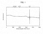
- FIG. 1 shows the ESR spectrum of a ⁇ -sialon not containing Eu.
- There is a close relationship between the absorption line intensity and the visible light absorption by the material. As the absorption lines in the vicinity of g 2 become smaller, the visible light absorption by the material also becomes smaller, and the material becomes more transparent.
- Eu ions exist in the divalent state and the trivalent state.
- uniform and broad light emission is achieved by virtue of transitions between the 4f orbit and the 5d orbit, and the outermost 5d electrons are greatly affected by adjacent anions. Therefore, fluorescence emission wavelengths vary with host crystals.
- Light emission from Eu 3+ is caused by transitions within the 4f-4f orbits. Therefore, the light emission involves intense emission lines. Also, since the transitions are within the 4f-4f orbits shielded by the outermost electrons, the light emission is not easily affected by adjacent anions.
- FIG. 3 shows the ESR spectrum of Eu 2 O 3 containing only Eu 3+ , and no absorption lines were observed.
- the fluorescence spectrum was measured by using a spectrophotofluorometer (F7000, manufactured by Hitachi High-Technologies Corporation).
- the excitation wavelength was 455 nm, which was of blue light, and the peak intensity and peak wavelength of the fluorescence spectrum were determined. Since the peak intensity varies with measurement devices and conditions, comparisons between examples and comparative examples were made based on the values relative to the peak intensity of YAG:Ce (P46-Y3, manufactured by Mitsubishi Chemical Corporation) measured under the same conditions.
- the peak intensity of the ⁇ -sialon of Example 1 was 230%, and the peak wavelength was 540 nm.
- Example 2 a ⁇ -sialon was manufactured in the same manner as in Example 1, except that the atmosphere in the heat treatment process was a gas containing 95% of argon and 5% of hydrogen.
- Comparative Example 1 a ⁇ -sialon was manufactured in the same manner as in Example 1, except that the atmosphere in the heat treatment process was an argon gas.
- Example 3 ⁇ -sialons were manufactured in the same manner as in Example 1, except that the z value of the ⁇ -sialon of Example 3 was 0.10, the z value of the ⁇ -sialon of Example 4 was 0.40, and the z value of the ⁇ -sialon of Example 5 was 1.0.
- the evaluation results are shown in Table 2.
- Example 2 a ⁇ -sialon was manufactured in the same manner as in Example 1, except that the holding temperature in the ⁇ -sialon calcination process was 1800°C, and the holding time was four hours.
- the evaluation results are shown in Table 3.
- Example 1 2000°C ⁇ 10h 0.48 3.4 4.7 4.2 9.1 ⁇ 10 15 230 540
- Comparative Example 2 1800°C ⁇ 4h 0.46 0.2 4.7 4.3 1.3 ⁇ 10 16 56 535
- Comparative Example 2 is the same as Example 1 in the total Eu content. In Comparative Example 2, however, since the amount of Eu 2+ solid-solved in the ⁇ -sialon crystals was very small, P2 was very low, and the fluorescence intensity was remarkably low.
- Example 6 An example of a light emitting device as another aspect of the invention is now described as Example 6.
- the light emitting device of Example 6 is a white LED that was manufactured in the following manner.
- the silicone resin was potted in a surface-mount package to which a blue LED element having a peak wavelength of 450 nm was bonded. Thermal curing was further performed, to form the white LED.
- a white LED was manufactured using the phosphor of Comparative Example 1.
- Example 6 and Comparative Example 3 were made to emit light under the same energization conditions, and the center illuminances and chromaticities (CIE1931) under the same conditions were measured with a luminance meter.
- the center illuminance in Example 6 was 8% higher than the center illuminance in Comparative Example 3.
- Example 6 As another example, an image display apparatus using the light emitting device of Example 6 as the backlight for a liquid crystal panel is now described. Since this image display apparatus had a liquid crystal panel using a brighter backlight, images were more brightly displayed.
- Example 6 As yet another example, a lighting apparatus using the light emitting device of Example 6 is now described. This lighting apparatus exhibited a higher illuminance.
Landscapes
- Chemical & Material Sciences (AREA)
- Inorganic Chemistry (AREA)
- Engineering & Computer Science (AREA)
- Materials Engineering (AREA)
- Organic Chemistry (AREA)
- Physics & Mathematics (AREA)
- Nonlinear Science (AREA)
- Mathematical Physics (AREA)
- Crystallography & Structural Chemistry (AREA)
- General Physics & Mathematics (AREA)
- Optics & Photonics (AREA)
- Luminescent Compositions (AREA)
- Led Device Packages (AREA)
Abstract
Description
- The present invention relates to a β-sialon to be used as a phosphor that can be used in a light emitting device including a blue light-emitting diode or an ultraviolet light-emitting diode, and to a light emitting device and applications thereof.
- Patent Document 1 discloses an Eu-containing β-sialon that can be used as a phosphor for a white LED and the like and as a green-yellow light emitting component in a light emitting device. A β-sialon is a phosphor containing Eu2+ in its crystalline structure, and the Eu2+ is excited by ultraviolet-blue light. This phosphor emits green-yellow light, having a peak wavelength of 520 to 560 nm.
Patent Document 2 discloses a technique for improving the luminous efficiency of an Eu-containing β-sialon. - Patent Document 1: Japanese Patent Publication No.
3,921,545 - Patent Document 2: International Publication No.
WO2008/062781 - An object of the present invention is to provide a β-sialon having a higher peak intensity in fluorescence measurement. Another object of the present invention is to provide a light emitting device, an image display apparatus, and an illuminating apparatus that use a β-sialon having a higher peak intensity in fluorescence measurement so as to emit brighter light.
- The present invention is a β-sialon expressed by the general formula, Si6-zAlzOzN8-z:Eu (0 < z < 4.2), with P2/P1 being not lower than 0.5 and not higher than 1000 (P1 representing the height of an absorption line appearing in the region where g is 2.00 ± 0.02 in a first derivative spectrum obtained by an electron spin resonance technique at 25°C, P2 representing the difference between the maximum value and the minimum value in a spectrum on the lower magnetic field side of P1).
- P2/P1 is preferably not lower than 1.9 and not higher than 1000.
- Both the maximum value and the minimum value in the spectrum on the lower magnetic field side of the β-sialon preferably appear in the region where g is not smaller than 3.5 and not greater than 6.0.
- The spin density corresponding to an absorption line appearing in the region where g is 2.00 ± 0.02 in the electron spin resonance spectrum of the β-sialon at 25°C is preferably 6 × 10¹⁶ spins/g or lower.
- The Eu content of the β-sialon is preferably not smaller than 0.1% by mass and not larger than 3% by mass.
- The "peak wavelength when blue light having a wavelength of 450 nm is emitted" in the β-sialon is preferably not shorter than 520 nm and not longer than 560 nm, and the half-value width of the fluorescence spectrum is preferably not smaller than 45 nm and not greater than 70 nm.
- Another aspect of the invention is a light emitting device that includes: a light emitting source; and a wavelength converting member mounted on the light emitting face of the light emitting source, the above described β-sialon being provided in the wavelength converting member.
- Yet another aspect of the invention is an image display apparatus that includes: a liquid crystal panel; and a backlight for the liquid crystal panel, the backlight including the above light emitting device.
- Still another aspect of the invention is a lighting apparatus that includes the above light emitting device.
- A β-sialon according to the present invention has a higher peak intensity in fluorescence measurement. Since the β-sialon has a higher peak intensity in fluorescence measurement, a light emitting device, an image display apparatus, and a lighting apparatus emit brighter light, using the β-sialon.
-
-
FIG. 1 shows the ESR spectrum of a β-sialon not containing Eu. -
FIG. 2 shows the ESR spectrum of a β-sialon containing Eu. -
FIG. 3 shows the ESR spectrum of an europium oxide powder. -
FIG. 4 shows the ESR spectrum of a β-sialon of Example 1. -
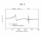
FIG. 5 shows the ESR spectra of β-sialons of Example 2 and Comparative Example 1. - The present invention is a β-sialon that is expressed by the general formula, Si6-zAlzOzN8-z:Eu (0 < z < 4.2), with P2/P1 being not lower than 0.5 and not higher than 1000 (P1 representing the height of an absorption line appearing in the region where g is 2.00 ± 0.02 in a first derivative spectrum obtained by an electron spin resonance technique at 25°C, P2 representing the difference between the maximum value and the minimum value in a spectrum on the lower magnetic field side of P1).
- P1 in the present invention represents the height of an absorption line that appears in the region where g is 2.00 ± 0.02 in a first derivative spectrum obtained by an electron spin resonance technique (hereinafter referred to as an ESR technique) at 25°C, and is specifically shown as P1 in
FIG. 4 . P2 in the present invention represents the difference between the maximum value and the minimum value in a spectrum on the lower magnetic field side of P1, and is specifically shown as P2 inFIG. 4 . - The β-sialon is identified by P2/P1 in the present invention, based on the following findings. If P2/P1 is too low, crystal defects existing in the β-sialon absorb visible light not causing emission of light, and the Eu2+ amount involved in fluorescence emission tends to become smaller, resulting in a lower fluorescence emission efficiency. If P2/P1 is too high, the solid solubility of Eu2+ into the β-sialon and the decrease of crystal defects in the β-sialon are restricted. Specifically, P2/P1 is not lower than 0.5 and not higher than 1000, or more preferably, not lower than 1.9 and not higher than 1000.
- An ESR technique is a spectrometric analysis to observe transitions that occur between levels when unpaired electrons are located in a magnetic field. Specifically, the energy level of unpaired electrons is split by a Zeeman effect in a magnetic field, and the unpaired electrons absorb the electromagnetic waves of the energy equivalent to the split width of the energy levels. Information about the number of existing unpaired electrons (the number of spins), the states of those unpaired electrons and the like is obtained from the absorption intensity of the absorption spectrum obtained by an ESR technique, and from the intensity of the magnetic field and the frequency of the electromagnetic waves at the time of absorption.
- The g value used in the ESR technique is one of the parameters according to ESR techniques, and is obtained by assigning the frequency (v) of the electromagnetic waves and the resonant magnetic field (H) to a resonance condition equation (hv = gβH). Here, h represents the Planck's constant (6.626 × 10⁻³⁴ J·s), and β represents Bohr magnetons (9.274 × 10⁻²⁴ J·T-1). In the case of free electrons, the g value having a relativistic correction made thereto is 2.0023. Actual unpaired electrons are subject to spin orbit interactions, and therefore, have a specific g value.
- Both the maximum value and the minimum value in a spectrum on the lower magnetic field side of the β-sialon preferably appear in the region where g is not smaller than 3.5 and not greater than 6.0, so as to obtain an excellent fluorescence emission efficiency. This range is preferred, because the fluorescence emission efficiency is dramatically improved by achieving a proper ratio between the absorption line intensity in the vicinity of the point of g = 2 based on the crystal defects in the β-sialon in the ESR spectrum of the Eu-containing β-sialon, and the absorption line intensity in the vicinity of the point of g = 5 based on Eu2+, which is solid-solved in the β-sialon and contributes to fluorescence emission.
- The β-sialon of the present invention is manufactured in the following manner. Raw materials are mixed at a high temperature to generate a β-sialon, and the β-sialon is subjected to a heat treatment process. The heat treatment process may be performed in a vacuum or an inert atmosphere in which the partial pressure of nitrogen is low, so that unpaired electrons that exist in the vicinity of the point where g is 2 and are measured by an ESR spectrum technique can be reduced. Further, the heat treatment atmosphere may be a reducing atmosphere. Accordingly, the effect to reduce the amount of unpaired electrons in the vicinity of the point where g is 2 can be made larger, and the spectrum intensity in the vicinity of the point where g is 5 can be made higher.
- The spin density corresponding to an absorption line appearing in the region where g is 2.00 ± 0.02 in the electron spin resonance spectrum of the β-sialon at 25°C is preferably 6 × 10¹⁶ spins/g or lower. The spin density is the value per unit mass obtained by dividing the number of spins measured by an ESR technique by the sample mass used in the measurement, and the number of spins in the vicinity of the point where g is 2 is closely related to crystal defects. This is because, when the spin density becomes higher, the amount of exiting unpaired electrons that cause a decrease in luminous efficiency tends to becomes larger, and therefore, the β-sialon host crystals tend to absorb light that does not cause light emission.
- The Eu content of the β-sialon is preferably not smaller than 0.1% by mass and not larger than 3% by mass, so that P2/P1 of the ESR spectrum easily falls within the range mentioned above.
- The β-sialon of the present invention is used in a light emitting device that includes a light emitting source and a phosphor. The β-sialon of the present invention has light emission characteristics such that absorption lines appear in the wavelength region of 520 to 560 nm particularly when ultraviolet light or visible light having a wavelength of 350 to 500 nm is used as the excitation source for irradiation. Accordingly, where a ultraviolet LED or a blue LED is appropriately combined with a phosphor that emits orange-red light and/or a phosphor that emits blue light as needed, white light is generated.
- The "peak wavelength where blue light with a wavelength of 450 nm is emitted" in the β-sialon is preferably not shorter than 520 nm and not longer than 560 nm, and the half-value width of the fluorescence spectrum is preferably not smaller than 45 nm and not greater than 70 nm.
- From the viewpoint of fluorescence emission, the β-sialon may be a mixture containing a certain amount of noncrystalline phase or some other crystalline phase as long as the characteristics are not degraded. However, the β-sialon preferably contains the largest possible amount of β-sialon crystalline phase with a high purity, and is preferably formed with a single phase.
- If the mean particle size of the β-sialon is too small, the light absorptance tends to become lower due to particle dispersion, and uniform dispersion in the resin sealing the LED tends to become difficult. If the mean particle size is too large, the intensity of emission and the color tone tend to vary. Therefore, the mean particle size is preferably not smaller than 1 µm and not larger than 30 µm.
- Another aspect of the invention is a light emitting device that includes a light emitting source and a wavelength converting member mounted on the light emitting face of the light emitting source, with the above described β-sialon being provided in the wavelength converting member.
- The light emitting device of the present invention includes at least one light emitting source and a phosphor including the β-sialon of the present invention. The light emitting source is preferably an LED or a fluorescent lamp. This light emitting device has light emission characteristics such that absorption lines appear in the wavelength region of 520 to 560 nm when ultraviolet light or visible light is used as the excitation source, for example. Accordingly, this light emitting device can generate white light by appropriately combining a ultraviolet LED or a blue LED with a phosphor that emits orange-red light and/or a phosphor that emits blue light, as needed. The emission wavelength of ultraviolet light is normally 350 to 500 nm, and the emission wavelength of blue light is normally 440 to 480 nm.
- In the light emitting device, the above described β-sialon may be used independently as a phosphor, or may be used together with a phosphor that has different light emission characteristics. The β-sialon of the present invention may also be combined with a nitride or oxynitride phosphor having a small decrease in luminance at high temperatures, such as an Eu-containing α-sialon orange phosphor or a CaAlSiN3:Eu red phosphor. In this manner, color rendering properties and color reproducibility are improved.
- Yet another aspect of the invention is an image display apparatus that includes a liquid crystal panel and a backlight for the liquid crystal panel, with the backlight including the above described light emitting device. Using the above described light emitting device, this image display apparatus serves as a liquid crystal display apparatus with preferred color reproducibility.
- Still another aspect of the invention is a lighting apparatus that includes the above described light emitting device. Using the above described light emitting device, this lighting apparatus serves as any kind of indoor lighting with preferred color rendering properties.
- Referring now to the drawings and tables, examples of β-sialons according to the present invention are described in detail in conjunction with comparative examples.
- A β-sialon according to Example 1 is expressed by the general formula, Si6-zAlzOzN8-z (z = 0.2), and contains Eu as the light emission center, with P2/P1 being 3.4, P1 representing the height of an absorption line appearing in the region where g is 2.00 ± 0.02 in a first derivative spectrum obtained by an electron spin resonance technique at 25°C, P2 representing the difference between the maximum value and the minimum value in a spectrum on the lower magnetic field side of P1.
-
FIG. 4 shows ESR spectrum of the β-sialon of Example 1. P2/P1 (in the expression, P1 represents the height of an absorption line appearing in the region where g is 2.00 ± 0.02 in a first derivative spectrum obtained by an electron spin resonance technique at 25°C, and P2 represents the difference between the maximum value and the minimum value in a spectrum on the lower magnetic field side of P1) was 3.4. The g values (gmax and gmin) at which the maximum value and the minimum value of the spectrum on the lower magnetic field side appeared were 4.7 and 4.2, respectively. The spin density that corresponded to the absorption in the region where g was 2.00 ± 0.02 and was quantitated with the use of a standard sample was 9.1 × 10¹⁵ spins/g. - When powder X-ray diffraction measurement (XRD) using a Kα-line of Cu was carried out on the β-sialon of Example 1, the only existing crystalline phase was the β-sialon. The Eu content determined by an ICP emission spectrometric analysis was 0.48% by mass.
- A method of manufacturing the β-sialon includes a calcination process for calcining mixed starting materials, a heat treatment process to be performed after the calcined materials are turned into powder, and an acid treatment process for removing impurities from the heat-treated powder.
- An α-silicon nitride powder (manufactured by Ube Industries, Ltd., Grade SN-E10), a nitride aluminum powder (manufactured by Tokuyama Corporation, Grade E), and an aluminum oxide powder (manufactured by Taimei Chemicals Co., Ltd., Grade TM-DAR) were combined, so that the z value of the Eu-containing β-sialon (Si6-zAlzOzN8-z:Eu) after the synthesis became 0.2. Further, 0.8% in outer percentage by mass of an europium oxide powder (manufactured by Shin-Etsu Chemicals Co, Ltd., Grade Ru) was combined with those powders, to obtain a raw material mixture.
- Using a nylon pot and silicon nitride balls, dry ball mill mixing was performed on the raw material mixture. After that, the mixture was put through a sieve with a sieve aperture of 150 µm, to remove aggregation substance and obtain a raw material powder.
- A cylindrical container made of boron nitride with a lid (manufactured by Denki Kagaku Kogyo Kabushiki Kaisha, Grade N-1) was filled with the raw material powder, and a 10-hour calcination was performed at 2000°C in a 0.8 MPa pressurized nitrogen atmosphere in an electric furnace having a carbon heater, to obtain a product material of the β-sialon. After lightly cracked, the product material was put through a sieve with a sieve aperture of 45 µm, to obtain a product powder of the β-sialon.
- A cylindrical container made of boron nitride was filled with the product powder, and a 6-hour heat treatment was performed at 1500°C in a hydrogen-flow atmosphere at atmospheric pressure in an electric furnace having a tungsten heater in which the furnace is entirely made of metals. As a result, a heat-treated powder of the β-sialon was obtained. The metals in the furnace in this example are tungsten and molybdenum forming furnace components.
- The heat-treated powder of the β-sialon was then immersed in a mixed acid of hydrofluoric acid and nitric acid. After that, decantation to remove the supernatant and fine powder was repeated until the liquid solution became neutral. The resultant precipitate was filtered and dried, and was further put through a sieve with a sieve aperture of 45 µm, to obtain the β-sialon of Example 1.
- Next, 50 mg of the obtained β-sialon was put into an ESR sample tube, and ESR measurement was carried out at room temperature. In the measurement, a "JES-FE2XG ESR measurement apparatus", manufactured by JEOL Ltd., was used.
- The measurement conditions for determining P2/P1 were as follows:
- Magnetic field sweep range: 0 to 5000 gausses (0 to 500 mT)
- Magnetic field modulation: 100 kHz, 5 gausses
- Radiated electromagnetic waves: 10 mW, 9.2 GHz (subjected to fine adjustment in each measuring operation, so as to achieve a resonant frequency)
- The measurement conditions for determining the spin density were as follows:
- Magnetic field sweep range: 3050 to 3550 gausses (305 to 355 mT)
- Radiated electromagnetic waves: 10 mW, 9.2 GHz (subjected to fine adjustment in each measuring operation, so as to achieve a resonant frequency)
- The g value of an absorption line was determined from the frequency of the radiated electromagnetic waves and the magnetic field intensity, according to a resonance condition equation. The g value of the absorption line was determined based on the peak position of the above described Mn2+ standard sample.
-
FIG. 4 shows the ESR spectrum of the β-sialon of Example 1. Where P1 represented the height of an absorption line appearing in the region where g was 2.00 ± 0.02 while P2 represented the difference between the maximum value and the minimum value in a spectrum on the lower magnetic field side of P1, P2/P1 was 3.4. The g values (gmax and gmin) of the maximum value and the minimum value of the spectrum on the lower magnetic field side were 4.7 and 4.2, respectively. The spin density that corresponded to the absorption in the region where g was 2.00 ± 0.02 and was quantitated with the use of the standard sample was 9.1 × 10¹⁵ spins/g. - For a comparison purpose,
FIG. 1 shows the ESR spectrum of a β-sialon not containing Eu. The six small absorption lines in the vicinity of g = 2 in the graph were due to the Mn2+ contained in the standard sample for quantitating a g value and a spin density. The β-sialon has a large number of crystal defects having unpaired electrons almost in a free electron state, and, as shown inFIG. 1 , distinct absorption lines are observed in the vicinity of g = 2. There is a close relationship between the absorption line intensity and the visible light absorption by the material. As the absorption lines in the vicinity of g = 2 become smaller, the visible light absorption by the material also becomes smaller, and the material becomes more transparent. - To develop the function of a phosphor, the Eu2+ contained in the β-sialon crystals has unpaired electrons in the 4f orbit, and accordingly, can be quatitated by an ESR technique. The electronic state of Eu2+ is affected by its coordination environment, and therefore, the positions of the absorption lines in an ESR spectrum vary with host crystals.
FIG. 2 shows the ESR spectrum of a β-sialon containing Eu. Not only the absorption lines in the vicinity of g = 2 caused by the crystal defects in the β-sialon shown inFIG. 1 , but also absorption lines caused by the unpaired electrons of Eu2+ are observed in the vicinity of g = 5 with lower magnetic field. - Eu ions exist in the divalent state and the trivalent state. In the case of Eu2+, uniform and broad light emission is achieved by virtue of transitions between the 4f orbit and the 5d orbit, and the outermost 5d electrons are greatly affected by adjacent anions. Therefore, fluorescence emission wavelengths vary with host crystals. Light emission from Eu3+ is caused by transitions within the 4f-4f orbits. Therefore, the light emission involves intense emission lines. Also, since the transitions are within the 4f-4f orbits shielded by the outermost electrons, the light emission is not easily affected by adjacent anions.
- Unlike Eu2+, Eu3+ cannot have absorption lines detected by an ESR technique at room temperature.
FIG. 3 shows the ESR spectrum of Eu2O3 containing only Eu3+, and no absorption lines were observed. - The fluorescence spectrum of an Eu-containing β-sialon is uniform and broad, and no intense emission lines are observed. Therefore, only Eu2+ is involved in light emission. Accordingly, a spectrum in the vicinity of g = 5 as measured by an ESR technique indicates information about Eu2+ contributing to fluorescence emission.
- When powder X-ray diffraction measurement (XRD) using a Kα-line of Cu was carried out on the β-sialon of Example 1, the only existing crystalline phase was the β-sialon. The Eu content determined by an ICP emission spectrometric analysis was 0.48% by mass.
- The fluorescence spectrum was measured by using a spectrophotofluorometer (F7000, manufactured by Hitachi High-Technologies Corporation). The excitation wavelength was 455 nm, which was of blue light, and the peak intensity and peak wavelength of the fluorescence spectrum were determined. Since the peak intensity varies with measurement devices and conditions, comparisons between examples and comparative examples were made based on the values relative to the peak intensity of YAG:Ce (P46-Y3, manufactured by Mitsubishi Chemical Corporation) measured under the same conditions. The peak intensity of the β-sialon of Example 1 was 230%, and the peak wavelength was 540 nm.
- The evaluation results are shown in Table 1.
[Table 1] Heat treatment atmosphere Eu content (% by mass) ESR measurement Fluorescence measurement P2/P1 gmax gmin g=2 spin density (spins/g) Peak intensity (%) Peak wave length (nm) Example 1 H2 0.48 3.4 4.7 4.2 9.1×10¹⁵ 230 540 Example 2 Ar+5%H2 0.51 0.91 4.7 4.2 3.2×10¹⁶ 225 540 Comparative Example 1 Ar 0.50 0.42 4.7 4.2 7.4×10¹⁶ 200 542 - In Example 2, a β-sialon was manufactured in the same manner as in Example 1, except that the atmosphere in the heat treatment process was a gas containing 95% of argon and 5% of hydrogen.
- In Comparative Example 1, a β-sialon was manufactured in the same manner as in Example 1, except that the atmosphere in the heat treatment process was an argon gas.
- As shown in Table 1, the fluorescence peak intensity was higher where P2/P1 was higher.
- In Examples 3 through 5, β-sialons were manufactured in the same manner as in Example 1, except that the z value of the β-sialon of Example 3 was 0.10, the z value of the β-sialon of Example 4 was 0.40, and the z value of the β-sialon of Example 5 was 1.0. The evaluation results are shown in Table 2.
[Table 2] z value of raw material Eu content (% by mass) ESR measurement Fluorescence measurement P2/P1 gmax gmin g=2 spin density (sp i ns/g) Peak intensity (%) Peak wavelength (nm) Example 1 0.20 0.48 3.4 4.7 4.2 9.1×10¹⁵ 230 540 Example 3 0.10 0.32 9.8 4.7 4.3 3.1×10¹⁵ 245 535 Example 4 0.40 0.52 35.5 4.7 4.2 1.5×10¹⁵ 238 544 Example 5 1.0 0.34 11.3 4.6 4.2 5.2×10¹⁵ 215 550 - Improving the fluorescence characteristics by making P2/P1 higher was effective in the range of the z values of the β-sialons of Examples 1 and 3 through 5.
- In Comparative Example 2, a β-sialon was manufactured in the same manner as in Example 1, except that the holding temperature in the β-sialon calcination process was 1800°C, and the holding time was four hours. The evaluation results are shown in Table 3.
[Table 3] Calcination temperature x time Eu content (% by mass) ESR measurement Fluorescence measurement P2/P1 gmax gmin g=2 spin density (spins/g) Peak intensity (%) Peak wavelength (nm) Example 1 2000°C × 10h 0.48 3.4 4.7 4.2 9.1×10¹⁵ 230 540 Comparative Example 2 1800°C×4h 0.46 0.2 4.7 4.3 1.3×10¹⁶ 56 535 - Comparative Example 2 is the same as Example 1 in the total Eu content. In Comparative Example 2, however, since the amount of Eu2+ solid-solved in the β-sialon crystals was very small, P2 was very low, and the fluorescence intensity was remarkably low.
- An example of a light emitting device as another aspect of the invention is now described as Example 6.
- The light emitting device of Example 6 is a white LED that was manufactured in the following manner. The phosphor of Example 1 and a red phosphor (the emission peak wavelength: 650 nm) having the composition, Ca0.992Eu0-08AlSiN3, were added to silicone resin. After subjected to defoaming and kneading, the silicone resin was potted in a surface-mount package to which a blue LED element having a peak wavelength of 450 nm was bonded. Thermal curing was further performed, to form the white LED. In a comparative example (Comparative Example 3), a white LED was manufactured using the phosphor of Comparative Example 1.
- The light emitting devices of Example 6 and Comparative Example 3 were made to emit light under the same energization conditions, and the center illuminances and chromaticities (CIE1931) under the same conditions were measured with a luminance meter. As a result of a comparison between the center illuminances in white light emitting devices having the chromaticity coordinates (x, y) at (0.31, 0.32), the center illuminance in Example 6 was 8% higher than the center illuminance in Comparative Example 3.
- As another example, an image display apparatus using the light emitting device of Example 6 as the backlight for a liquid crystal panel is now described. Since this image display apparatus had a liquid crystal panel using a brighter backlight, images were more brightly displayed.
- As yet another example, a lighting apparatus using the light emitting device of Example 6 is now described. This lighting apparatus exhibited a higher illuminance.
Claims (9)
- A β-sialon expressed by the general formula, Si6-zAlzOzN8z:Eu (0 < z < 4.2), with P2/P1 being not lower than 0.5 and not higher than 1000 (P1 representing a height of an absorption line appearing in a region where g is 2.00 ± 0.02 in a first derivative spectrum obtained by an electron spin resonance technique at 25°C, P2 representing a difference between a maximum value and a minimum value in a spectrum on a lower magnetic field side of P1).
- The β-sialon according to claim 1, wherein P2/P1 is not lower than 1.9 and not higher than 1000.
- The β-sialon according to clam 1, wherein both the maximum value and the minimum value in the spectrum on the lower magnetic field side of the β-sialon appear in a region where g is not smaller than 3.5 and not greater than 6.0.
- The β-sialon according to any one of claims 1 to 3, wherein a spin density corresponding to the absorption line appearing in the region where g is 2.00 ± 0.02 in an electron spin resonance spectrum of the β-sialon at 25°C is 6 × 10¹⁶ spins/g or lower.
- The β-sialon according to any one of claims 1 to 4, wherein the Eu content of the β-sialon is not smaller than 0.1% by mass and not larger than 3% by mass.
- The β-sialon according to any of claims 1 to 5, wherein, when blue light having a wavelength of 450 nm is emitted, a peak wavelength of the β-sialon is not shorter than 520 nm and not longer than 560 nm, and a half-value width of a fluorescence spectrum thereof is not smaller than 45 nm and not greater than 70 nm.
- A light emitting device comprising:a light emitting source; anda wavelength converting member mounted on a light emitting face of the light emitting source, whereinthe β-sialon according to any one of claims 1 to 6 is provided in the wavelength converting member.
- An image display apparatus comprising:a liquid crystal panel; anda backlight for the liquid crystal panel, whereinthe backlight includes the light emitting device according to claim 7.
- A lighting apparatus comprising the light emitting device according to claim 7.
Applications Claiming Priority (2)
| Application Number | Priority Date | Filing Date | Title |
|---|---|---|---|
| JP2010275625 | 2010-12-10 | ||
| PCT/JP2011/059781 WO2012077368A1 (en) | 2010-12-10 | 2011-04-21 | β TYPE SIALON, LIGHT-EMITTING DEVICE AND APPLICATION THEREOF |
Publications (2)
| Publication Number | Publication Date |
|---|---|
| EP2662430A1 true EP2662430A1 (en) | 2013-11-13 |
| EP2662430A4 EP2662430A4 (en) | 2014-10-22 |
Family
ID=46206876
Family Applications (1)
| Application Number | Title | Priority Date | Filing Date |
|---|---|---|---|
| EP11847735.5A Withdrawn EP2662430A4 (en) | 2010-12-10 | 2011-04-21 | BETA TYPE SIALON, LIGHT EMITTING DEVICE AND ITS APPLICATION |
Country Status (7)
| Country | Link |
|---|---|
| US (1) | US9028719B2 (en) |
| EP (1) | EP2662430A4 (en) |
| JP (1) | JP5443597B2 (en) |
| KR (1) | KR101334560B1 (en) |
| CN (1) | CN102656249B (en) |
| TW (1) | TWI518168B (en) |
| WO (1) | WO2012077368A1 (en) |
Cited By (1)
| Publication number | Priority date | Publication date | Assignee | Title |
|---|---|---|---|---|
| JP2014122304A (en) * | 2012-12-21 | 2014-07-03 | Toshiba Corp | Yellow phosphor and method for manufacturing the same |
Families Citing this family (5)
| Publication number | Priority date | Publication date | Assignee | Title |
|---|---|---|---|---|
| EP2664660A4 (en) * | 2010-09-16 | 2014-03-05 | Denki Kagaku Kogyo Kk | BETA-TYPE SIALON, METHOD FOR PRODUCING THE SAME, AND LIGHT-EMITTING DEVICE |
| CN105331361B (en) * | 2015-12-03 | 2017-09-19 | 河北利福光电技术有限公司 | A kind of β SiAlON: Eu2+Green emitting phosphor and its synthetic method |
| JP7507018B2 (en) * | 2020-07-03 | 2024-06-27 | デンカ株式会社 | Method for manufacturing β-type sialon phosphor, method for manufacturing wavelength conversion member, and method for manufacturing light emitting device |
| JP7676175B2 (en) * | 2021-03-24 | 2025-05-14 | デンカ株式会社 | β-type sialon phosphor powder and light-emitting device |
| JP2022148407A (en) * | 2021-03-24 | 2022-10-06 | デンカ株式会社 | METHOD FOR PRODUCING β-TYPE SIALON PHOSPHOR POWDER |
Family Cites Families (9)
| Publication number | Priority date | Publication date | Assignee | Title |
|---|---|---|---|---|
| JP4043981B2 (en) * | 2003-03-25 | 2008-02-06 | シャープ株式会社 | mobile phone |
| JP3921545B2 (en) * | 2004-03-12 | 2007-05-30 | 独立行政法人物質・材料研究機構 | Phosphor and production method thereof |
| JP2006344409A (en) * | 2005-06-07 | 2006-12-21 | Seiko Instruments Inc | Illumination device and display device including the same |
| TWI357927B (en) * | 2006-11-20 | 2012-02-11 | Denki Kagaku Kogyo Kk | Fluorescent substance and manufacturing method the |
| JP4974703B2 (en) | 2007-02-21 | 2012-07-11 | 富士フイルム株式会社 | Surface lighting device |
| JP5380052B2 (en) | 2008-11-25 | 2014-01-08 | パナソニック株式会社 | LED lighting device |
| JP5330889B2 (en) * | 2009-04-14 | 2013-10-30 | 電気化学工業株式会社 | LED module for lighting |
| EP2365047B1 (en) * | 2009-06-09 | 2014-02-26 | Denki Kagaku Kogyo Kabushiki Kaisha | ß-SIALON PHOSPHOR, USE THEREOF AND METHOD FOR PRODUCING SAME |
| EP2664660A4 (en) * | 2010-09-16 | 2014-03-05 | Denki Kagaku Kogyo Kk | BETA-TYPE SIALON, METHOD FOR PRODUCING THE SAME, AND LIGHT-EMITTING DEVICE |
-
2011
- 2011-04-21 WO PCT/JP2011/059781 patent/WO2012077368A1/en not_active Ceased
- 2011-04-21 CN CN201180004529.5A patent/CN102656249B/en active Active
- 2011-04-21 EP EP11847735.5A patent/EP2662430A4/en not_active Withdrawn
- 2011-04-21 KR KR1020127011491A patent/KR101334560B1/en active Active
- 2011-04-21 US US13/811,900 patent/US9028719B2/en active Active
- 2011-04-21 JP JP2012512105A patent/JP5443597B2/en active Active
- 2011-07-29 TW TW100126900A patent/TWI518168B/en active
Cited By (1)
| Publication number | Priority date | Publication date | Assignee | Title |
|---|---|---|---|---|
| JP2014122304A (en) * | 2012-12-21 | 2014-07-03 | Toshiba Corp | Yellow phosphor and method for manufacturing the same |
Also Published As
| Publication number | Publication date |
|---|---|
| CN102656249B (en) | 2014-07-16 |
| KR20120093920A (en) | 2012-08-23 |
| KR101334560B1 (en) | 2013-11-28 |
| CN102656249A (en) | 2012-09-05 |
| JP5443597B2 (en) | 2014-03-19 |
| TWI518168B (en) | 2016-01-21 |
| US9028719B2 (en) | 2015-05-12 |
| EP2662430A4 (en) | 2014-10-22 |
| TW201224117A (en) | 2012-06-16 |
| WO2012077368A1 (en) | 2012-06-14 |
| JPWO2012077368A1 (en) | 2014-05-19 |
| US20130120691A1 (en) | 2013-05-16 |
Similar Documents
| Publication | Publication Date | Title |
|---|---|---|
| JP4891336B2 (en) | Phosphor, method for manufacturing the same, and light emitting device | |
| EP3133135B1 (en) | Semiconductor light-emitting device | |
| CN1977030B (en) | Phosphors and Luminaires | |
| KR101168177B1 (en) | Phospher, process for producing the same and luminescence apparatus | |
| US9279079B2 (en) | Method of manufacturing phosphor, light-emitting device, and image display apparatus | |
| JP5110518B2 (en) | Phosphor, method of manufacturing the same, and lighting fixture | |
| KR101688337B1 (en) | Fluorophore, method for producing same, light-emitting device using fluorophore, image display device, pigment, and ultraviolet absorbent | |
| EP3992264B1 (en) | Fluorescent body, method for manufacturing same, and light-emitting device using same | |
| KR20080081058A (en) | Yellow light emitting phosphor and white light emitting device using the same | |
| KR20130106394A (en) | Blue-light-emitting phosphor and light-emitting device equipped with the blue-light-emitting phosphor | |
| JP2018002870A (en) | β TYPE SIALON PHOSPHOR AND METHOD FOR PRODUCING THE SAME AND LIGHT EMITTING DEVICE USING THE SAME | |
| US9028719B2 (en) | β- sialon, and light emitting device and applications thereof | |
| KR101417566B1 (en) | β-TYPE SIALON AND PRODUCTION METHOD THEREFOR AND LIGHT-EMITTING DEVICE | |
| KR101476561B1 (en) | Phosphor and light-emitting device | |
| EP3006539A1 (en) | Oxynitride phosphor powder | |
| JP7672735B2 (en) | Phosphor, its manufacturing method, light-emitting element, and light-emitting device | |
| JP2016088970A (en) | Phosphor, light emitting device, illumination device and image display device | |
| CN102933683B (en) | Method for producing B type sialon | |
| TWI443868B (en) | Method for producing β-type lanthanum aluminum oxynitride | |
| JP2012062394A (en) | Method of manufacturing beta type sialon |
Legal Events
| Date | Code | Title | Description |
|---|---|---|---|
| PUAI | Public reference made under article 153(3) epc to a published international application that has entered the european phase |
Free format text: ORIGINAL CODE: 0009012 |
|
| 17P | Request for examination filed |
Effective date: 20130522 |
|
| AK | Designated contracting states |
Kind code of ref document: A1 Designated state(s): AL AT BE BG CH CY CZ DE DK EE ES FI FR GB GR HR HU IE IS IT LI LT LU LV MC MK MT NL NO PL PT RO RS SE SI SK SM TR |
|
| DAX | Request for extension of the european patent (deleted) | ||
| A4 | Supplementary search report drawn up and despatched |
Effective date: 20140922 |
|
| RIC1 | Information provided on ipc code assigned before grant |
Ipc: G02F 1/1335 20060101ALI20140916BHEP Ipc: C09K 11/77 20060101ALI20140916BHEP Ipc: H01L 33/50 20100101ALI20140916BHEP Ipc: C09K 11/64 20060101AFI20140916BHEP Ipc: H05B 33/14 20060101ALI20140916BHEP Ipc: C09K 11/08 20060101ALI20140916BHEP |
|
| RAP1 | Party data changed (applicant data changed or rights of an application transferred) |
Owner name: DENKA COMPANY LIMITED |
|
| 17Q | First examination report despatched |
Effective date: 20160927 |
|
| STAA | Information on the status of an ep patent application or granted ep patent |
Free format text: STATUS: EXAMINATION IS IN PROGRESS |
|
| STAA | Information on the status of an ep patent application or granted ep patent |
Free format text: STATUS: THE APPLICATION IS DEEMED TO BE WITHDRAWN |
|
| 18D | Application deemed to be withdrawn |
Effective date: 20170627 |