EP2661096A1 - Method for monitoring an optical gate and associated equipment - Google Patents
Method for monitoring an optical gate and associated equipment Download PDFInfo
- Publication number
- EP2661096A1 EP2661096A1 EP12290153.1A EP12290153A EP2661096A1 EP 2661096 A1 EP2661096 A1 EP 2661096A1 EP 12290153 A EP12290153 A EP 12290153A EP 2661096 A1 EP2661096 A1 EP 2661096A1
- Authority
- EP
- European Patent Office
- Prior art keywords
- optical
- input
- output
- linked
- packet
- Prior art date
- Legal status (The legal status is an assumption and is not a legal conclusion. Google has not performed a legal analysis and makes no representation as to the accuracy of the status listed.)
- Granted
Links
- 230000003287 optical effect Effects 0.000 title claims abstract description 310
- 238000012544 monitoring process Methods 0.000 title claims abstract description 73
- 238000000034 method Methods 0.000 title claims abstract description 13
- 230000000903 blocking effect Effects 0.000 claims abstract description 32
- 230000001427 coherent effect Effects 0.000 claims description 12
- 238000010586 diagram Methods 0.000 description 16
- 238000005259 measurement Methods 0.000 description 11
- XUIMIQQOPSSXEZ-UHFFFAOYSA-N Silicon Chemical compound [Si] XUIMIQQOPSSXEZ-UHFFFAOYSA-N 0.000 description 6
- 229910052710 silicon Inorganic materials 0.000 description 5
- 239000010703 silicon Substances 0.000 description 5
- 238000005516 engineering process Methods 0.000 description 4
- 230000010287 polarization Effects 0.000 description 4
- 239000004065 semiconductor Substances 0.000 description 4
- 238000001514 detection method Methods 0.000 description 3
- 230000007423 decrease Effects 0.000 description 2
- 238000001914 filtration Methods 0.000 description 2
- 239000004973 liquid crystal related substance Substances 0.000 description 2
- 238000012806 monitoring device Methods 0.000 description 2
- 229910052691 Erbium Inorganic materials 0.000 description 1
- UYAHIZSMUZPPFV-UHFFFAOYSA-N erbium Chemical compound [Er] UYAHIZSMUZPPFV-UHFFFAOYSA-N 0.000 description 1
- 239000000835 fiber Substances 0.000 description 1
- HFGPZNIAWCZYJU-UHFFFAOYSA-N lead zirconate titanate Chemical compound [O-2].[O-2].[O-2].[O-2].[O-2].[Ti+4].[Zr+4].[Pb+2] HFGPZNIAWCZYJU-UHFFFAOYSA-N 0.000 description 1
- 230000001360 synchronised effect Effects 0.000 description 1
Images


Classifications
-
- H—ELECTRICITY
- H04—ELECTRIC COMMUNICATION TECHNIQUE
- H04Q—SELECTING
- H04Q11/00—Selecting arrangements for multiplex systems
- H04Q11/0001—Selecting arrangements for multiplex systems using optical switching
- H04Q11/0005—Switch and router aspects
-
- H—ELECTRICITY
- H04—ELECTRIC COMMUNICATION TECHNIQUE
- H04J—MULTIPLEX COMMUNICATION
- H04J14/00—Optical multiplex systems
- H04J14/02—Wavelength-division multiplex systems
- H04J14/0201—Add-and-drop multiplexing
- H04J14/0202—Arrangements therefor
- H04J14/0204—Broadcast and select arrangements, e.g. with an optical splitter at the input before adding or dropping
-
- H—ELECTRICITY
- H04—ELECTRIC COMMUNICATION TECHNIQUE
- H04J—MULTIPLEX COMMUNICATION
- H04J14/00—Optical multiplex systems
- H04J14/02—Wavelength-division multiplex systems
- H04J14/0201—Add-and-drop multiplexing
- H04J14/0202—Arrangements therefor
- H04J14/0205—Select and combine arrangements, e.g. with an optical combiner at the output after adding or dropping
-
- H—ELECTRICITY
- H04—ELECTRIC COMMUNICATION TECHNIQUE
- H04J—MULTIPLEX COMMUNICATION
- H04J14/00—Optical multiplex systems
- H04J14/02—Wavelength-division multiplex systems
- H04J14/0287—Protection in WDM systems
- H04J14/0293—Optical channel protection
- H04J14/0295—Shared protection at the optical channel (1:1, n:m)
-
- H—ELECTRICITY
- H04—ELECTRIC COMMUNICATION TECHNIQUE
- H04Q—SELECTING
- H04Q11/00—Selecting arrangements for multiplex systems
- H04Q11/0001—Selecting arrangements for multiplex systems using optical switching
- H04Q11/0062—Network aspects
- H04Q11/0066—Provisions for optical burst or packet networks
-
- H—ELECTRICITY
- H04—ELECTRIC COMMUNICATION TECHNIQUE
- H04Q—SELECTING
- H04Q11/00—Selecting arrangements for multiplex systems
- H04Q11/0001—Selecting arrangements for multiplex systems using optical switching
- H04Q11/0005—Switch and router aspects
- H04Q2011/0007—Construction
- H04Q2011/0009—Construction using wavelength filters
-
- H—ELECTRICITY
- H04—ELECTRIC COMMUNICATION TECHNIQUE
- H04Q—SELECTING
- H04Q11/00—Selecting arrangements for multiplex systems
- H04Q11/0001—Selecting arrangements for multiplex systems using optical switching
- H04Q11/0005—Switch and router aspects
- H04Q2011/0007—Construction
- H04Q2011/0013—Construction using gating amplifiers
-
- H—ELECTRICITY
- H04—ELECTRIC COMMUNICATION TECHNIQUE
- H04Q—SELECTING
- H04Q11/00—Selecting arrangements for multiplex systems
- H04Q11/0001—Selecting arrangements for multiplex systems using optical switching
- H04Q11/0005—Switch and router aspects
- H04Q2011/0007—Construction
- H04Q2011/0016—Construction using wavelength multiplexing or demultiplexing
-
- H—ELECTRICITY
- H04—ELECTRIC COMMUNICATION TECHNIQUE
- H04Q—SELECTING
- H04Q11/00—Selecting arrangements for multiplex systems
- H04Q11/0001—Selecting arrangements for multiplex systems using optical switching
- H04Q11/0005—Switch and router aspects
- H04Q2011/0037—Operation
- H04Q2011/0043—Fault tolerance
Definitions
- the present invention relates to the field of wavelength division multiplexing (WDM) optical network with packet granularity capability and more particularly to the optical gates used in the optical packet switching node in order to delete the data corresponding to the dropped packets.
- WDM wavelength division multiplexing
- optical packets are transmitted within time slots and, in each node called optical packet switching nodes, optical packets may be dropped and added.
- this time slot has to.be freed (the optical signal corresponding to the dropped optical packet has to be deleted) in order to prevent the superimposition of several signals within one time slot of one channel which would result in a signal impossible to decode.
- optical gates capable of blocking and filtering out the light transmitted in a time slot of a channel are implemented in the node.
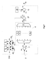
- Fig.1 represents a diagram of a packet add/drop structure 1 of an optical packet switching node 100 of the state of the art. It comprises a dropping optical coupler 3 comprising an input 301 linked to the input 2 of the packet add/drop structure 1, a first output 302 linked to a fast tunable receiver 5 which is configured for detecting the dropped packets and a second output 303 linked to the input 601 of a switching structure 6, the dropping optical coupler 3 being configured for transmitting a wavelength division multiplexed (WDM) signal received on its input 301 to both its first 302 and its second 303 outputs.
- WDM wavelength division multiplexed
- the switching structure 6 comprises a demultiplexer 7 configured for demultiplexing the multiplexed channels of the WDM signal into a plurality of channels which are transmitted respectively to a plurality of optical gates 9 configured for blocking or letting pass the packets of the time slots of each channel.
- the different channels are re-multiplexed by a multiplexer 11.
- the packet add/drop structure 1 also comprises a fast tunable transmitter 15 which is configured to emit signals corresponding to the added packets aimed at being inserted in the time slots freed or emptied by the optical gates 9.
- An adding optical coupler 13 comprising a first input 131 linked to the output 602 of the switching structure 6, a second input 132 linked to the fast tunable transmitter 15 and an output 133 linked to the output 18 of the packet add/drop structure 1, the said adding optical coupler 13 being configured to mix the signals received from its first 131 and its second 132 inputs and for transmitting the mixed signal to its output 133.
- optical gates 9 is crucial in such packet add/drop structures 1 so that their correct functioning needs to be monitored regularly to detect as soon as possible a failure occurring on an optical gate 9.
- a solution to this problem is to add a photodetector, such as a photodiode, at the output of each optical gate 9 in order to measure the optical power level at the output of each gate and report the value of this power level to a control board in real-time.
- a photodetector such as a photodiode
- the optical gates may be integrated in a chip
- either the photodetectors are also integrated on-chip which would means that a failure occurring on the chip would likely lead to a failure of both the optical gates and the monitoring components, i.e. the photodetectors.
- a solution is to implement the photodetectors off-chip but this solution would require a plurality of additional optical wires between the chip and the photodetectors which is difficult to implement and leads to additional costs.
- the present invention refers to a method for monitoring an optical gate of a packet add/drop structure of an optical packet switching node of a wavelength division multiplexing optical network, the packet add/drop structure comprising:
- the embodiments of the present invention also refer to a packet add/drop structure of an optical packet switching node of a wavelength division multiplexing optical network, the packet add/drop structure comprising:
- inventions of the present invention of the present invention also refer to an optical packet switching node comprising at least one packet add/drop structure.
- the elements having the same reference correspond to elements having a similar function.
- the reference number designates the class of element having a common function and the index defines a particular elements of the class.
- WSS Wavelength Selective Switch
- SOA Semiconductor Optical Amplifier
- time slot in a packet stream transmitted in a channel refers to a time interval wherein a packet is inserted.
- the time slot duration corresponds to the duration of a packet and an inter-packet gap duration;
- the term "dropped packet” refers to a packet for which the current node is the egress node so that the said packet is detected by a receiver and the data of the packet are decoded by the receiver. Inversely, the non-dropped packets are transmitted transparently toward another node.
- the embodiments of the present invention refer to the monitoring of optical gates of a packet add/drop structure of an optical packet switching node using a fast tunable receiver of the node.
- An optical gate being configured to let a received signal pass when being in a passing state and for filtering a received signal out when being in a blocking state.
- the embodiments of the present invention can be divided into two modes.
- a first mode optical gates are monitored during a dedicated time slot called control time slot while in a second mode, the monitoring is achieved while the monitored optical gates work normally.
- a time slot is reserved for the monitoring of the optical gates whenever a monitoring of the optical gates is needed.
- This time slot is called control time slot and refers to a time wherein an optical signal without data is sent on the channel associated with an optical gate that needs to be monitored and wherein a predetermined switching scheme is applied to the monitored optical gates and the power level measured in each position of the monitored optical gate is compared with predetermined thresholds.
- a control time slot may be scheduled at predetermined time intervals according to a required failure detection time and/or a maximum proportion of control time slot with respect to the data time slot so that the throughput reduction is less than a predetermined value.
- three different nodes are used for the monitoring of the optical gates of one of these optical nodes.
- Fig.2 represents an example of a network portion comprising three optical packet switching nodes 100 noted N1, N2 and N3. Intermediate nodes may be located between N1 and N2 or between N2 and N3 and these three nodes may be part of an optical ring. Furthermore, it is assumed that node N1 comprises transmitters for sending optical signals simultaneously on the plurality of wavelength channels associated with the plurality of optical gates that need to be monitored. For example, in the case of a ring network, one node is usually dedicated to the emission of signals on all the channels and the other nodes have fast tunable transmitters 15 to add new packets in the freed time slots of the dropped packets. However, the time slots of the different channels may also be filled with light by several nodes.
- the structure of the packet add/drop structures 1 of the packet switching nodes Ni remains as described in fig.1 and the monitored optical gates are the optical gates of the packet add/drop structure of node N2.
- the transmitters of node N1 are configured to apply a control time slot.
- the application of this control time slot corresponds to the sending of dummy packets (optical signal without data) on each wavelength associated with an optical gate that needs to be monitored. If all the optical gates of node N2 are monitored during a control time, all the channels are fed with light in node N1 during a control time slot.
- a predetermined sequential switching scheme is applied to the optical gates of node N2. In this sequential switching scheme, the monitored optical gates are set, one after the other, successively in a blocking and in a passing state during predetermined amounts of time.
- the optical gates when they are not monitored during the control time slot, they are set in a passing state (or passing mode) in order to reduce the amount of time when no light is transmitted.
- some optical components such as Erbium Doped Fiber Amplifiers (EDFAs) require a steady optical power level to function properly so that time intervals without light need to be avoided.
- EDFAs Erbium Doped Fiber Amplifiers
- the first optical gate 9 1 starts to be monitored in a passing state during a time interval ⁇ t 2 corresponding to the time required for a fast tunable receiver to do the measurement of the optical power level, herein called measurement time interval.
- sequential switching scheme it is meant that the monitored optical gates are monitored one after the other (there is no need for a predetermined order in the sequence, for example the optical 9 2 may be monitored before the optical gate 9 1 )
- the optical gate 9 1 is set in a blocking state during another measurement time interval ⁇ t 2 to do the monitoring of the blocking state.
- the optical gate 9 1 has been monitored on each state and is set to a passing state.
- the time to transmit the signal from the optical gate 9 1 to the fast tunable receiver has to be considered as this travelling time is not negligible, especially if the optical gate and the fast tunable receiver are located in different nodes.
- the monitoring in a passing state of the optical gate 9 1 will be performed at time t 1 + ⁇ t t by the fast tunable receiver.
- the travelling time necessary for the light to go from the optical gate to the fast tunable receiver is therefore taken into account to achieve a monitoring at the right time, that is to say when the optical gate is in the state that needs to be monitored.
- the fast tunable receiver is then tuned at the wavelength corresponding to the channel associated with the optical gate 9 2 which requires a time interval ⁇ t 1 .
- the optical gate 9 2 is then monitored in the passing state during a time interval ⁇ t 2 and in a blocking state during a time interval ⁇ t 2 .
- the time intervals ⁇ t 1 and ⁇ t 2 may be adjusted so that the end of the monitoring matches with the end of the time slot.
- the durations required to switch the optical gates from one state to the other have also to be considered and taken into account to determine the measurement time intervals, for example if this switching time of an optical gate is ⁇ t s , the monitoring of the optical gate 9 1 in a passing state will start at time t 1 + ⁇ t t + ⁇ t s .
- the optical power level is measured during the measurement time interval ⁇ t 2 shifted of the travelling time ⁇ t t necessary for the signal to go from node N2 to node N3 and possibly of a switching time ⁇ t s .
- the measured optical power level is then compared to a first predetermined threshold when the measurement corresponds to the monitoring of an optical gate in a passing state and to a second predetermined threshold when the measurement corresponds to the monitoring of an optical gate in a blocking state.
- Fig.4 shows a diagram with two threshold Th1 and Th2 used for the monitoring of the optical gate 9 1 .
- the optical gate 9 1 is supposed to be in a passing state.
- the monitored optical gate 9 1 is supposed to be in a blocking state.
- the measured optical power level is therefore compared with the second threshold Th2 and if the measured power level is higher than the second threshold Th2, the monitored optical gate is considered to have a failure on the blocking state.
- the blocking state may be monitored before the passing state.
- the passing state of all the optical gates is monitored during a first time interval and the blocking state of all the optical gates is monitored during a second time interval, however, such scheme is longer as the fast tunable receiver has to be tuned a larger number of time.
- the optical gates can be set in a blocking state when they are not monitored during a measurement time interval, for example before time t 1 and after time t 3 in the case of the optical gate 9 1 .
- this first embodiment enables the monitoring of the optical gates without adding additional hardware components with respect to a packet add/drop structure of a packet switching node of the state of the art.
- the fast tunable receiver used for the monitoring is located in the same node as the optical gates to be monitored. Indeed, having the receiver in a different node may lead to issues such as synchronization issues or adding more complexity to control the monitoring of the optical gates.
- Fig.5 represents a diagram of a packet add-drop structure 101 according to the second embodiment of the present invention.
- This packet add/drop structure 101 differs from the packet/add drop structure 1 of the state of the art described in Fig.1 in that it comprises an additional optical coupler, herein called monitoring optical coupler 17 comprising an input 171 linked to the output 602 of the switching structure 6, a first output 173 linked to a first input 192 of a two-to-one switch, herein called dropping two-to-one switch 19 and a second output 172 linked to the input 131 of the adding optical coupler 13.
- This monitoring optical coupler 17 is configured for transmitting the signal received on its input 171 toward both its a first 172 and second 173 outputs.
- the dropping two-to-one switch 19 comprises an output 191 linked to the fast tunable receiver 5 and a second input 193 linked to the first output 302 of the dropping optical coupler 3.
- This dropping two-to-one switch 19 is configured for transmitting the signal coming from the monitoring optical coupler 17 and blocking the signal coming from the dropping optical coupler 3 when optical gates 9 of the switching structure 6 are monitored, i.e. during a control time slot, and for transmitting the signal coming from the dropping optical coupler 3 and blocking the signal coming from the monitoring optical coupler 17 otherwise.
- the sequential switching scheme is the same as for the first embodiment and the only additional step concerns the switching of the dropping two-to-one switch 19 at time to of the start of the control time slot and at the time t e of the end of the control time slot.
- the only additional hardware components with respect to a packet add/drop structure of the state of the art is the dropping two-to-one switch 19, the monitoring optical coupler 17 which are cheap components so that the cost of the implementation of the monitoring according to this second embodiment remains low.
- the transmitter used for emitting optical signal during the control time slot is located in the same node as the optical gates to be monitored so that all the equipments necessary for the monitoring are gathered in a single node.
- Fig.6 represents a diagram of a packet add-drop structure 201 according to the third embodiment of the present invention.
- This packet add/drop structure 201 differs from the packet/add drop structure 101 of the second embodiment described in Fig.4 in that it comprises an additional two-to-one switch, herein called adding two-to-one switch 21 and an additional one-to-two switch, herein called adding one-to-two switch 23.
- the adding two-to-one switch 21 comprises a first input 212 linked to the input 2 of the packet add-drop structure 201, a second input 213 linked to a first output 232 of an adding one-to-two switch 23 and an output 211 linked to the input 301 of the dropping optical coupler 3,
- the adding one-to-two switch 23 comprises an input 231 linked to the fast tunable transmitter 15 and a second output 233 linked to the second input 132 of the adding optical coupler 13.
- the adding two-to-one switch 21 is configured for transmitting the signal coming from the adding one-to-two switch 23 and blocking the signal coming from the input 2 when optical gates of the switching structure 6 are monitored, i.e. during a control time slot, and for transmitting the signal coming from the input 2 and blocking the signal coming from the adding one-to-two switch 23 otherwise.
- the adding one-to-two switch 23 is configured for transmitting the signal coming from the fast tunable transmitter 15 toward the adding two-to-one switch 21 when optical gates of the switching structure 6 are monitored, i.e. during a control time slot, and toward the adding optical coupler 13 otherwise.
- the sequential switching scheme is the same as for the second embodiment and the only additional steps concern the switching of the adding two-to-one switch 21 and the adding one-to-two switch 23 at time to of the start of the control time slot and at the time t e of the end of the control time slot.
- the fast tunable transmitter 15 comprises a plurality of transmitters tuned to the plurality of wavelengths corresponding to the channels associated with the monitored optical gates or the fast tunable transmitter is tuned sequentially to each wavelength corresponding to each channel associated with a monitored optical gate.
- this last option may be applied only if there is no component of the network that are affected by variations in the optical power level. Indeed, for each channel, only a fraction time ⁇ t 2 of the time slot will be fed with light.
- the only additional hardware components with respect to a packet switching node of the state of the art are the dropping two-to-one switch 19, the monitoring optical coupler 17, the adding two-to-one switch 21 and the adding one-to-two switch 23 which are cheap components so that the cost of the implementation of the monitoring according to this third embodiment remains low.
- the embodiments of the first mode enable therefore monitoring a high number of optical gates of a switching structure 6 within a single time slot so that such monitoring enables a fast failure detection with a limited impact on the network performance.
- This second mode relies on the fact that in a packet switching node, there exists most of the time an idle fast tunable receiver, either because the idle fast tunable receiver is reserved for protection in case of failure on a working receiver or because an optical packet switching node usually comprises a plurality of packet add/drop structures comprising each a fast tunable receiver but when the traffic decreases, a packet add/drop structure may remain in an idle state.
- a packet add/drop structure may comprise several fast tunable receivers and one may be in an idle state when the traffic decreases.
- the idea is to use a fast tunable receiver in an idle state to achieve the monitoring of the optical gates.
- an additional fast tunable receiver may be dedicated to the monitoring.
- the fast tunable receiver used for the monitoring is linked to the output of the switching structure comprising the optical gates that need to be monitored.
- the fast tunable receiver used for the monitoring is then tuned sequentially to the wavelengths corresponding to the channels associated with the monitored optical gates and the optical power level is measured for each wavelength.
- the optical power level measured by the fast tunable receiver used for the monitoring is then compared to predetermined thresholds according to the state of the monitored optical gate at the time of measurement.
- predetermined thresholds according to the state of the monitored optical gate at the time of measurement.
- an optical gate is in a passing state when the idle fast tunable receiver is tuned to the wavelength corresponding to the channel associated with this optical gate, the monitoring will be achieved on the passing state only.
- a state of an optical gate may not be monitored during a relatively large amount of time if the optical gate is always in the other state during monitoring.
- the idle fast tunable receiver used for the monitoring may be located in a subsequent node.
- all the optical gates may be monitored within a single time slot (if the number of optical gates to monitor is not too large with respect to the fast tunable receiver switching and measuring capacities) but only one state is monitored for each optical gate.
- Fig.7 represents a diagram of a packet add-drop structure 310 according to a fourth embodiment of the present invention wherein a fast tunable receiver 5 b is reserved for protection.
- This packet add/drop structure 310 differs from the packet/add drop structure 1 described in Fig. 1 in that it comprises a first and a second fast tunable receivers 5 a and 5 b , a first and a second additional one-to-two switch 25 a and 25 b and an additional optical coupler, herein called monitoring optical coupler 27.
- the second fast tunable receiver 5 b is used for protection in case of failure of the first fast tunable receiver 5 a .
- the second fast tunable receiver 5 b is therefore idle when the first fast tunable receiver 5 a works correctly.
- the first one-to-two switch 25 a comprises an input 253 linked to the first output 302 of the dropping optical coupler 3, a first output 251 linked to the first tunable receiver 5 a and a second output 252 linked to the second fast tunable receiver 5 b .
- the first one-to-two switch 25 a is configured to route or to transmit a signal received from the dropping optical coupler 3 toward one of the fast tunable receiver 5 a or 5 b .
- the monitoring optical coupler 27 comprises an input 271 linked to the output 602 of the switching structure 6, a first output 272 linked to the first input 131 of the adding optical coupler 13 and a second output 273 linked to the input 256 of the second one-to-two switch 25 b .
- the monitoring optical coupler 27 is configured to transmit a signal received from the switching structure 6 toward both the optical coupler 13 and the second one-to-two switch 25 b .
- the second one-to-two switch 25 b comprises a first 254 and a second 255 outputs linked respectively to the first 5 a and the second 5 b fast tunable receivers.
- the second one-to-two switch 25 b is configured to transmit a signal received from the monitoring optical coupler 27 toward one of the fast tunable receivers 5 a or 5 b .
- the first and second one-to-two switches 25 a and 25 b are synchronized so that when the first one-to-two switch 25 a transmits a signal toward the first fast tunable receiver 5 a , the second one-to-two switch 25 b transmits a signal toward the second fast tunable receiver 5 b and conversely.
- the first and second one-to-two switches 25 a and 25 b may be replaced by a two-to-two switch which would be configured accordingly.
- the first tunable receiver 5 a receives the signal coming from the dropping optical coupler 3 and detect the optical packets that need to be dropped while the second fast tunable receiver 5 b receives the signal coming from the optical coupler 27 and is tuned sequentially to the wavelength corresponding to the channels associated with optical gates 9 of the switching structure 6 and for each wavelength, the second fast tunable receiver 5 b measures the optical power level and compare this level with predetermined thresholds according to the state of the monitored optical gate 9.
- an optical gate 9 is in a blocking state and the measured optical power level is above a first predetermined threshold, the blocking state of the monitored optical gate 9 is considered as faulty whereas if an optical gate 9 is in a passing state and the measured optical power level is below a second predetermined threshold, the passing state of the monitored optical gate 9 is considered as faulty.
- the signal received from the dropping optical coupler 3 is transmitted to the second fast tunable receiver 5 b by the first one-to-two switch 25 a and the second fast tunable receiver 5 b is then configured for detecting the dropped optical packets. No monitoring is possible anymore until the failure of the first fast tunable receiver 5 a is fixed. When the failure is fixed, the first tunable receiver 5 a can be used for the monitoring.
- a higher number of fast tunable receivers can be used with one of the fast tunable reserved for protection.
- the said idle fast tunable receiver can be used for the monitoring of the optical gates.
- Fig.8 represents a diagram of an optical packet switching node 100 comprising a plurality of packet add/drop structure 401 according to a fifth embodiment of the present invention. For sake of clarity, only two packet add/drop structure 401a and 401b are represented.
- packet add/drop structures 401 differ from the packet/add drop structure 1 of the state of the art described in Fig.1 in that it comprises an additional optical coupler herein called monitoring optical coupler 29, a N-to-one switch 31 and a one-to-L switch 33.
- the monitoring optical coupler 29 comprises an input 291 linked to the output 602 of the switching structure 6, a first output 292 linked to the first input 131 of the adding optical coupler 13 and a second output 293 linked to the input 331 of the one-to-L switch 33.
- the N-to-one switch 31 comprises an output 311 linked to the fast tunable receiver 5 and a plurality of inputs.
- One input is linked the first output 302 of the dropping optical coupler 3, another input is linked to an output of the one-to-L switch 33, the other inputs being linked to an output of a one-to-L switch 33 of another packet add/drop structures 401, for example the packet add/drop structure 401b in the present case.
- the one-to-L switch 33 comprises a plurality of outputs linked respectively to an input of a N-to-one switch 31 of a packet add/drop structures 401.
- the monitoring optical coupler 29 is configured to transmit the signal received from the switching structure 6 to both the adding optical coupler 13 and the one-to-L switch 33.
- the one-to-L switch 33 is configured for transmitting the signal received from the monitoring optical coupler 29 to an idle fast tunable receiver 5 of one of the plurality of packet add/drop structures 401.
- the monitoring of the optical gates 9 is then achieved by the idle fast tunable receiver 5 in the same way as the fast tunable receiver 5 reserved for the protection in the fourth embodiment. If no fast tunable receiver 5 is idle, for example when the packet switching node is used at its full capacity, no monitoring is achieved.
- the N-to-one switch 31 is configured for transmitting the signal received from the dropping optical coupler 3 when a signal to be processed is received at the input 2 of the packet add/drop structure 401 a and for monitoring the optical gates 9 of the switching structure 6 of one of the plurality of packet add/drop structures, for example the packet add/drop structure 401 b when no signal to be processed is received at the input 2 of the packet add/drop structure 401 a (a receiver of an idle packet add/drop structure may monitor the optical gates its own packet add/drop structure if an optical signal is transmitted through the idle switching structure). The monitoring may be performed so that during one time slot, an idle fast tunable receiver 5 monitors the optical gates of one working packet add/drop structure 401.
- an optical packet switching node comprises six packet add/drop structures 401 and if a fast tunable receiver 5 remains idle during five time slots, the idle fast tunable receiver 5 may monitor the optical gates 9 of the five other packet add/drop structures 401, the N-to-one switch 31 enabling to switch from one packet add/drop structure 401 to another between two time slots.
- other monitoring scheme may be applied depending on the number of optical gates per packet add/drop structure and the time required for the idle fast tunable receiver 5 to monitor each optical gate.
- the embodiments of the second mode enable therefore to monitor optical gates of a switching structure 6 whenever a fast tunable receiver 5 of an optical packet switching node 100 remains idle which is particularly often in case of bursty traffic or in case of additional fast tunable receivers 5 used for protection. Furthermore, the cost of the required additional equipments remains limited and the performance of the network is not impacted.
- the multiplexers and demultiplexers may be implemented as array waveguide gratings (AWG) based either on a semi-conductor 3-5 technology, a planar silicium technology or silicon photonics technology.
- ASG array waveguide gratings
- WSS wavelength Selective Switches
- MEMS micro-mechanical systems
- LcoS liquid crystals on silicon
- the optical gates are implemented preferably as semiconductor optical amplifier (SOA) gates.
- SOA semiconductor optical amplifier
- MZM Mach-Zehnder modulators
- ring resonators acousto-optic switches
- LCDoS liquid crystal on silicon
- MEMS micro-electromechanical systems
- the switching structure 6 comprising the demultiplexer 7, the optical gates 9 and the multiplexer 11 may be integrated according to different options:
- the x-to-x switches may be implemented as directional optical coupler with index change capability of the optical guide to create or not a matching with the incoming optical signal such as a Polarized Lead Zirconium Titanate (PLZT) directional coupler or as an active coupler comprising a passive optical coupler combined with optical gates at each output of the passive optical coupler or as a waveguides network with an active guide to select the output port for the received signal.
- PZT Polarized Lead Zirconium Titanate
- the fast tunable transmitters may be implemented as a fast tunable continuous wave (CW) laser or as an array of lasers emitting at wavelengths corresponding to the different channels coupled to a fast selector or a filter that selects at least one of the wavelength to be transmitted.
- CW continuous wave
- the fast tunable receivers may be implemented either as a coherent receiver (36) or as an array of receivers combined with a demultiplexer, each receiver being tuned to one of the wavelengths corresponding to one of the received channels and the demultiplexer being configured to distribute the different received channels respectively toward the receivers of the array.
- Fig.10 represents the functional elements of an embodiment of a coherent receiver 36.
- the coherent receiver 36 comprises an input 38 that receives a signal comprising a plurality of multiplexed channels.
- the input 38 is linked to a first input of a coherent mixer 40.
- the second input of the coherent mixer 40 is linked to a local oscillator 41 implemented as a fast tunable laser which is tuned, for each time slot, to the wavelength corresponding to the channel that comprises a packet that needs to be dropped or a signal that needs to be measured.
- the local oscillator 41 may be implemented by an array of lasers emitting a set of wavelengths corresponding to the channels of the band and coupled to a fast selector (the number of lasers in the array being equal to the number of channels that can be processed).
- the coherent mixer 40 comprises for instance a polarization beam splitter (PBS), a 50/50 optical splitter, and two 90° optical hybrids.
- the polarization beam splitter is configured for splitting the signal received at the input 38 into two signals having orthogonal polarizations.
- the 50/50 optical splitter is configured to split the signal received from the local oscillator 41 in two signals having half power each.
- One output of the PBS and one output of the 50/50 splitter are sent to a 90° hybrid coupler.
- the other PBS output and the other output of the 50/50 splitter are sent to the second 90° optical hybrid. Therefore, the inphase and quadrature components of both polarizations are retrieved at the outputs of the coherent mixer 40.
- photo-detectors 43 are then detected by four photo-detectors 43, generally implemented as balanced photodiodes, which are linked respectively to four analogical to digital (A/D) converters 45.
- A/D analogical to digital
- the obtained four digital signals are then used to feed digital signal processing means 47 that are configured for retrieving the encoded data.
- the establishment of a control time slot and the use of a fast tunable receiver as measurement device for the optical power level of the signal outputted by the optical gates during the control time slot as well as the use of an idle fast tunable receiver as measuring device for the optical power level of the signal outputted by the optical gates enable to monitor the optical gates of the packet add/drop structures of the optical packet switching nodes without requiring expensive additional equipments.
- a failure can be detected in a short amount of time and the network performance are either barely or not impacted by the monitoring.
- the monitoring device is not integrated on a common chip as the equipments to be monitored and a plurality of additional wires to connect the monitoring device with the control board are not required.
Landscapes
- Engineering & Computer Science (AREA)
- Computer Networks & Wireless Communication (AREA)
- Signal Processing (AREA)
- Optical Communication System (AREA)
Abstract
- a switching structure (6) comprising a demultiplexer (7) linked to an input (601) of the switching structure (6), a multiplexer (11) linked to an output (602) of the switching structure (6) and a plurality of optical gates (9) set in parallel between the demultiplexer (7) and the multiplexer (11), an optical gate (9) being configured to filter out, in a blocking state, or to let pass, in a passing state, a packet received by the optical gate (9), wherein the output of the switching structure (6) is also transmitted to a fast tunable receiver (5) which is configured for:
- being tuned to a wavelength corresponding to a channel for which an associated optical gate (9) is monitored,
- measuring the optical power level of that said wavelength at the output (602) of the switching structure (6),
- comparing the measured optical power level with at least one predetermined threshold according to the state of the monitored optical gate (9).
Description
- The present invention relates to the field of wavelength division multiplexing (WDM) optical network with packet granularity capability and more particularly to the optical gates used in the optical packet switching node in order to delete the data corresponding to the dropped packets.
- Indeed, in network with packet granularity capability, optical packets are transmitted within time slots and, in each node called optical packet switching nodes, optical packets may be dropped and added. Thus, in order to add a new packet in a time slot to replace a dropped packet, this time slot has to.be freed (the optical signal corresponding to the dropped optical packet has to be deleted) in order to prevent the superimposition of several signals within one time slot of one channel which would result in a signal impossible to decode. To overcome this issue, optical gates capable of blocking and filtering out the light transmitted in a time slot of a channel are implemented in the node.
-
Fig.1 represents a diagram of a packet add/drop structure 1 of an opticalpacket switching node 100 of the state of the art. It comprises a droppingoptical coupler 3 comprising aninput 301 linked to theinput 2 of the packet add/drop structure 1, afirst output 302 linked to a fasttunable receiver 5 which is configured for detecting the dropped packets and asecond output 303 linked to theinput 601 of aswitching structure 6, the droppingoptical coupler 3 being configured for transmitting a wavelength division multiplexed (WDM) signal received on itsinput 301 to both its first 302 and its second 303 outputs. Theswitching structure 6 comprises ademultiplexer 7 configured for demultiplexing the multiplexed channels of the WDM signal into a plurality of channels which are transmitted respectively to a plurality ofoptical gates 9 configured for blocking or letting pass the packets of the time slots of each channel. At the output of theoptical gates 9, the different channels are re-multiplexed by amultiplexer 11. The packet add/drop structure 1 also comprises a fasttunable transmitter 15 which is configured to emit signals corresponding to the added packets aimed at being inserted in the time slots freed or emptied by theoptical gates 9. An addingoptical coupler 13 comprising afirst input 131 linked to theoutput 602 of theswitching structure 6, asecond input 132 linked to the fasttunable transmitter 15 and anoutput 133 linked to theoutput 18 of the packet add/drop structure 1, the said addingoptical coupler 13 being configured to mix the signals received from its first 131 and its second 132 inputs and for transmitting the mixed signal to itsoutput 133. - As a consequence, the role of the
optical gates 9 is crucial in such packet add/drop structures 1 so that their correct functioning needs to be monitored regularly to detect as soon as possible a failure occurring on anoptical gate 9. - In the state of the art, a solution to this problem is to add a photodetector, such as a photodiode, at the output of each
optical gate 9 in order to measure the optical power level at the output of each gate and report the value of this power level to a control board in real-time. - However, two problems arise with such solution.
- First, such solution requires the use of additional hardware components (i.e. photodiodes).
- Second, as the optical gates may be integrated in a chip, either the photodetectors are also integrated on-chip which would means that a failure occurring on the chip would likely lead to a failure of both the optical gates and the monitoring components, i.e. the photodetectors. In order to prevent this issue, a solution is to implement the photodetectors off-chip but this solution would require a plurality of additional optical wires between the chip and the photodetectors which is difficult to implement and leads to additional costs.
- It is therefore an object of the present invention to overcome the above mentioned drawbacks of the state of the art and to provide a solution for monitoring the optical gates of a packet add/drop structure with components that work independently of the optical gates and without requiring expensive additional hardware components.
- Thus, the present invention refers to a method for monitoring an optical gate of a packet add/drop structure of an optical packet switching node of a wavelength division multiplexing optical network, the packet add/drop structure comprising:
- a switching structure comprising a demultiplexer linked to an input of the switching structure, a multiplexer linked to an output of the switching structure and a plurality of optical gates set in parallel between the demultiplexer and the multiplexer, an optical gate being configured to filter out, in a blocking state, or to let pass, in a passing state, a packet received by the optical gate,
wherein the output of the switching structure is also transmitted to a fast tunable receiver which is configured for: - being tuned to a wavelength corresponding to a channel for which an associated optical gate is monitored,
- measuring the optical power level of that said wavelength at the output of the switching structure,
- comparing the measured optical power level with at least one predetermined threshold according to the state of the monitored optical gate.
- The embodiments of the present invention also refer to a packet add/drop structure of an optical packet switching node of a wavelength division multiplexing optical network, the packet add/drop structure comprising:
- at least one fast tunable receiver,
- a switching structure comprising a demultiplexer linked to an input of the switching structure, a multiplexer linked to an output of the switching structure and a plurality of optical gates set in parallel between the demultiplexer and the multiplexer, an optical gate being configured to filter out, in a blocking state, or to let pass, in a passing state, a packet received by the optical gate,
wherein the output of the switching structure is connected to one of the at least one fast tunable receiver, the said fast tunable receiver being configured for: - receiving a signal outputted by the switching structure when an optical gate of the switching structure is monitored,
- being tuned to a wavelength corresponding to the channel for which an optical gate is monitored,
- measuring the optical power level of that said wavelength at the output of the switching structure,
- comparing the measured optical power level with at least one predetermined threshold according to the state of the monitored optical gate.
- The embodiments of the present invention of the present invention also refer to an optical packet switching node comprising at least one packet add/drop structure.
-
-
FIG.1 is a diagram of a packet add-drop structure of the state of the art; -
FIG.2 is a diagram of a network portion comprising three nodes; -
FIG.3 is a diagram of the states of the optical gates of a packet add/drop structure during a predetermined sequential switching scheme according to some embodiments of the present invention; -
FIG.4 is a diagram of the thresholds used to determined the correct functioning of an optical gate; -
FIG.5 is a diagram of a packet add/drop structure according to a first embodiment of the present invention; -
FIG.6 is a diagram of a packet add/drop structure according to a second embodiment of the present invention; -
FIG.7 is a diagram of a packet add/drop structure according to a third embodiment of the present invention; -
FIG.8 is a diagram of an optical switching node comprising packet add/drop structures according to a fourth embodiment of the present invention; -
FIG.9 is a diagram of the functional elements of a coherent receiver; - In these drawings, the elements having the same reference correspond to elements having a similar function. Furthermore, with elements composed of a reference number and an index, the reference number designates the class of element having a common function and the index defines a particular elements of the class.
- As used herein, the term "WSS" refers to the acronym Wavelength Selective Switch;
- As used herein, the term "SOA" refers to the acronym Semiconductor Optical Amplifier;
- As used herein, the term "time slot" in a packet stream transmitted in a channel refers to a time interval wherein a packet is inserted. The time slot duration corresponds to the duration of a packet and an inter-packet gap duration;
- As used herein, the term "dropped packet" refers to a packet for which the current node is the egress node so that the said packet is detected by a receiver and the data of the packet are decoded by the receiver. Inversely, the non-dropped packets are transmitted transparently toward another node.
- The embodiments of the present invention refer to the monitoring of optical gates of a packet add/drop structure of an optical packet switching node using a fast tunable receiver of the node. An optical gate being configured to let a received signal pass when being in a passing state and for filtering a received signal out when being in a blocking state.
- Furthermore, the embodiments of the present invention can be divided into two modes. In a first mode, optical gates are monitored during a dedicated time slot called control time slot while in a second mode, the monitoring is achieved while the monitored optical gates work normally. These two modes will now be described in detail.
- In this first mode, a time slot is reserved for the monitoring of the optical gates whenever a monitoring of the optical gates is needed. This time slot is called control time slot and refers to a time wherein an optical signal without data is sent on the channel associated with an optical gate that needs to be monitored and wherein a predetermined switching scheme is applied to the monitored optical gates and the power level measured in each position of the monitored optical gate is compared with predetermined thresholds. A control time slot may be scheduled at predetermined time intervals according to a required failure detection time and/or a maximum proportion of control time slot with respect to the data time slot so that the throughput reduction is less than a predetermined value.
- The number of optical gates that can be monitored within one time slot depends on the time necessary for the fast tunable receiver to be tuned to the wavelength of the channel associated with the monitored optical gate and the time required to achieve a power level measurement. For example, if we assume that it takes 50ns to a fast tunable receiver to switch from one wavelength to another and that it takes 10ns to the fast tunable receiver to measure the power level, then with a time slot of 10µs, the number of optical gates that can be monitored by one fast tunable receiver during one time slot is approximately hundred and forty (10µs/((50ns+10ns+10ns))=142.8 (two times 10ns for the two states of an optical gate).
- Thus, if it is assumed that all the optical gates can be monitored in one time slot (which means that the number of channels is smaller or equal than 142) and if the monitoring time has to be less than 1% of the overall operational time then 1 time slot every 100 time slots will be a control packet reserved for monitoring. With a packet duration of 10µs, the failure detection time is 1ms.
- According to a first embodiment, three different nodes are used for the monitoring of the optical gates of one of these optical nodes.
-
Fig.2 represents an example of a network portion comprising three opticalpacket switching nodes 100 noted N1, N2 and N3. Intermediate nodes may be located between N1 and N2 or between N2 and N3 and these three nodes may be part of an optical ring. Furthermore, it is assumed that node N1 comprises transmitters for sending optical signals simultaneously on the plurality of wavelength channels associated with the plurality of optical gates that need to be monitored. For example, in the case of a ring network, one node is usually dedicated to the emission of signals on all the channels and the other nodes have fasttunable transmitters 15 to add new packets in the freed time slots of the dropped packets. However, the time slots of the different channels may also be filled with light by several nodes. - In this embodiment, the structure of the packet add/
drop structures 1 of the packet switching nodes Ni (i=1..3) remains as described infig.1 and the monitored optical gates are the optical gates of the packet add/drop structure of node N2. - When a monitoring of the optical gates of node N2 is required, for example every 1ms or every 100 time slots, the transmitters of node N1 are configured to apply a control time slot. The application of this control time slot corresponds to the sending of dummy packets (optical signal without data) on each wavelength associated with an optical gate that needs to be monitored. If all the optical gates of node N2 are monitored during a control time, all the channels are fed with light in node N1 during a control time slot. When the signal corresponding to this control time slot is received at node N2, a predetermined sequential switching scheme is applied to the optical gates of node N2. In this sequential switching scheme, the monitored optical gates are set, one after the other, successively in a blocking and in a passing state during predetermined amounts of time.
- Furthermore, in the presented embodiment, when the optical gates are not monitored during the control time slot, they are set in a passing state (or passing mode) in order to reduce the amount of time when no light is transmitted. Indeed, some optical components such as Erbium Doped Fiber Amplifiers (EDFAs) require a steady optical power level to function properly so that time intervals without light need to be avoided.
-
Fig.3 represents an example of sequential switching scheme during a control time slot of a duration ΔT in the case of M optical gates noted 9i (i=1...M) associated with M channels. The state of an optical gate during the control time slot is represented by the level of the horizontal lines Li (i=1...M), when the level is high, corresponding to the mark p (p=passing), an optical gate is in a passing state and when the level is low, corresponding to the mark b (b=blocking), the optical gate is in a blocking state. For sake of clarity, only the states of four optical gates have been represented. The sequential switching scheme starts at time to with a time interval Δt1 which corresponds to the time required by a fast tunable receiver, located in node N3, to be tuned to the wavelength of the channel associated with theoptical gate 91 so that no monitoring is achieved during this time interval and all the optical gates 9x (x=1...M) are in a passing state. At time t1 (where t1=t0+Δt1), the firstoptical gate 91 starts to be monitored in a passing state during a time interval Δt2 corresponding to the time required for a fast tunable receiver to do the measurement of the optical power level, herein called measurement time interval. Furthermore, it has to be noted that by sequential switching scheme, it is meant that the monitored optical gates are monitored one after the other (there is no need for a predetermined order in the sequence, for example the optical 92 may be monitored before the optical gate 91) - At time t2 (where t2=t1+Δt2), the
optical gate 91 is set in a blocking state during another measurement time interval Δt2 to do the monitoring of the blocking state. - Thus, at time t3, the
optical gate 91 has been monitored on each state and is set to a passing state. In practise, the time to transmit the signal from theoptical gate 91 to the fast tunable receiver has to be considered as this travelling time is not negligible, especially if the optical gate and the fast tunable receiver are located in different nodes. Thus, if the travelling time is Att, the monitoring in a passing state of theoptical gate 91 will be performed at time t1+Δtt by the fast tunable receiver. the travelling time necessary for the light to go from the optical gate to the fast tunable receiver is therefore taken into account to achieve a monitoring at the right time, that is to say when the optical gate is in the state that needs to be monitored. The fast tunable receiver is then tuned at the wavelength corresponding to the channel associated with theoptical gate 92 which requires a time interval Δt1. Theoptical gate 92 is then monitored in the passing state during a time interval Δt2 and in a blocking state during a time interval Δt2. This switching scheme is then applied sequentially on each optical gate 9x (x=1...M) until time te which corresponds either to the time when all the optical gates 9x (x=1...M) have been monitored or the end of the control time slot. In practise, the time intervals Δt1 and Δt2 may be adjusted so that the end of the monitoring matches with the end of the time slot. Furthermore, in practice, the durations required to switch the optical gates from one state to the other have also to be considered and taken into account to determine the measurement time intervals, for example if this switching time of an optical gate is Δts, the monitoring of theoptical gate 91 in a passing state will start at time t1+Δtt+ Δts. - At the fast tunable receiver, the optical power level is measured during the measurement time interval Δt2 shifted of the travelling time Δtt necessary for the signal to go from node N2 to node N3 and possibly of a switching time Δts. The measured optical power level is then compared to a first predetermined threshold when the measurement corresponds to the monitoring of an optical gate in a passing state and to a second predetermined threshold when the measurement corresponds to the monitoring of an optical gate in a blocking state.
Fig.4 shows a diagram with two threshold Th1 and Th2 used for the monitoring of theoptical gate 91. The power level is measured by the fast tunable receiver between time t1' and t2', with t1'=t1+Δtt+ Δts and t2'=t2+Δtt+ Δts. During this time interval, theoptical gate 91 is supposed to be in a passing state. Thus, if the measured optical power level is lower than the first predetermined threshold Th1 during this time interval (tl'-t2'), the monitoredoptical gate 91 is considered to have a failure on the passing state. Then, the power level is measured by the fast tunable receiver between time t2' and t3' with t3'=t3+Δtt+ Δts . During this time interval, the monitoredoptical gate 91 is supposed to be in a blocking state. The measured optical power level is therefore compared with the second threshold Th2 and if the measured power level is higher than the second threshold Th2, the monitored optical gate is considered to have a failure on the blocking state. - Besides, it has to be noted that the blocking state may be monitored before the passing state.
- Furthermore, according to another switching scheme, the passing state of all the optical gates is monitored during a first time interval and the blocking state of all the optical gates is monitored during a second time interval, however, such scheme is longer as the fast tunable receiver has to be tuned a larger number of time.
- It has also to be noted that if the components used in the network are not affected by variations of the optical power level, the optical gates can be set in a blocking state when they are not monitored during a measurement time interval, for example before time t1 and after time t3 in the case of the
optical gate 91. Thus, this first embodiment enables the monitoring of the optical gates without adding additional hardware components with respect to a packet add/drop structure of a packet switching node of the state of the art. - According to a second embodiment, the fast tunable receiver used for the monitoring is located in the same node as the optical gates to be monitored. Indeed, having the receiver in a different node may lead to issues such as synchronization issues or adding more complexity to control the monitoring of the optical gates.
-
Fig.5 represents a diagram of a packet add-drop structure 101 according to the second embodiment of the present invention. This packet add/drop structure 101 differs from the packet/adddrop structure 1 of the state of the art described inFig.1 in that it comprises an additional optical coupler, herein called monitoringoptical coupler 17 comprising aninput 171 linked to theoutput 602 of the switchingstructure 6, afirst output 173 linked to afirst input 192 of a two-to-one switch, herein called dropping two-to-oneswitch 19 and asecond output 172 linked to theinput 131 of the addingoptical coupler 13. This monitoringoptical coupler 17 is configured for transmitting the signal received on itsinput 171 toward both its a first 172 and second 173 outputs. - The dropping two-to-one
switch 19 comprises anoutput 191 linked to thefast tunable receiver 5 and asecond input 193 linked to thefirst output 302 of the droppingoptical coupler 3. This dropping two-to-oneswitch 19 is configured for transmitting the signal coming from the monitoringoptical coupler 17 and blocking the signal coming from the droppingoptical coupler 3 whenoptical gates 9 of the switchingstructure 6 are monitored, i.e. during a control time slot, and for transmitting the signal coming from the droppingoptical coupler 3 and blocking the signal coming from the monitoringoptical coupler 17 otherwise. - Besides, it has to be noted that the different additional optical fibres used to link the different components and represented by the lines in the different diagram will not be detailed.
- In this embodiment, the sequential switching scheme is the same as for the first embodiment and the only additional step concerns the switching of the dropping two-to-one
switch 19 at time to of the start of the control time slot and at the time te of the end of the control time slot. - Thus, with this second embodiment the only additional hardware components with respect to a packet add/drop structure of the state of the art is the dropping two-to-one
switch 19, the monitoringoptical coupler 17 which are cheap components so that the cost of the implementation of the monitoring according to this second embodiment remains low. - According to a third embodiment, the transmitter used for emitting optical signal during the control time slot is located in the same node as the optical gates to be monitored so that all the equipments necessary for the monitoring are gathered in a single node.
-
Fig.6 represents a diagram of a packet add-drop structure 201 according to the third embodiment of the present invention. This packet add/drop structure 201 differs from the packet/adddrop structure 101 of the second embodiment described inFig.4 in that it comprises an additional two-to-one switch, herein called adding two-to-oneswitch 21 and an additional one-to-two switch, herein called adding one-to-twoswitch 23. - The adding two-to-one
switch 21 comprises afirst input 212 linked to theinput 2 of the packet add-drop structure 201, asecond input 213 linked to afirst output 232 of an adding one-to-twoswitch 23 and anoutput 211 linked to theinput 301 of the droppingoptical coupler 3, - The adding one-to-two
switch 23 comprises aninput 231 linked to the fasttunable transmitter 15 and asecond output 233 linked to thesecond input 132 of the addingoptical coupler 13. - The adding two-to-one
switch 21 is configured for transmitting the signal coming from the adding one-to-twoswitch 23 and blocking the signal coming from theinput 2 when optical gates of the switchingstructure 6 are monitored, i.e. during a control time slot, and for transmitting the signal coming from theinput 2 and blocking the signal coming from the adding one-to-twoswitch 23 otherwise. - The adding one-to-two
switch 23 is configured for transmitting the signal coming from the fasttunable transmitter 15 toward the adding two-to-oneswitch 21 when optical gates of the switchingstructure 6 are monitored, i.e. during a control time slot, and toward the addingoptical coupler 13 otherwise. - In this embodiment, the sequential switching scheme is the same as for the second embodiment and the only additional steps concern the switching of the adding two-to-one
switch 21 and the adding one-to-twoswitch 23 at time to of the start of the control time slot and at the time te of the end of the control time slot. - Concerning the fast
tunable transmitter 15, either the fasttunable transmitter 15 comprises a plurality of transmitters tuned to the plurality of wavelengths corresponding to the channels associated with the monitored optical gates or the fast tunable transmitter is tuned sequentially to each wavelength corresponding to each channel associated with a monitored optical gate. However, this last option may be applied only if there is no component of the network that are affected by variations in the optical power level. Indeed, for each channel, only a fraction time Δt2 of the time slot will be fed with light. - Thus, with this third embodiment the only additional hardware components with respect to a packet switching node of the state of the art are the dropping two-to-one
switch 19, the monitoringoptical coupler 17, the adding two-to-oneswitch 21 and the adding one-to-twoswitch 23 which are cheap components so that the cost of the implementation of the monitoring according to this third embodiment remains low. - The embodiments of the first mode enable therefore monitoring a high number of optical gates of a switching
structure 6 within a single time slot so that such monitoring enables a fast failure detection with a limited impact on the network performance. - This second mode relies on the fact that in a packet switching node, there exists most of the time an idle fast tunable receiver, either because the idle fast tunable receiver is reserved for protection in case of failure on a working receiver or because an optical packet switching node usually comprises a plurality of packet add/drop structures comprising each a fast tunable receiver but when the traffic decreases, a packet add/drop structure may remain in an idle state. In the same way, a packet add/drop structure may comprise several fast tunable receivers and one may be in an idle state when the traffic decreases. Thus, the idea is to use a fast tunable receiver in an idle state to achieve the monitoring of the optical gates. Alternatively, an additional fast tunable receiver may be dedicated to the monitoring.
- In this second mode, no control time slot is needed and the fast tunable receiver used for the monitoring is linked to the output of the switching structure comprising the optical gates that need to be monitored. The fast tunable receiver used for the monitoring is then tuned sequentially to the wavelengths corresponding to the channels associated with the monitored optical gates and the optical power level is measured for each wavelength. The optical power level measured by the fast tunable receiver used for the monitoring is then compared to predetermined thresholds according to the state of the monitored optical gate at the time of measurement. However, it has to be noted that in this mode only one state of an optical gate may be monitored within one time slot and this state cannot be chosen as it is imposed by the traffic. For example if an optical gate is in a passing state when the idle fast tunable receiver is tuned to the wavelength corresponding to the channel associated with this optical gate, the monitoring will be achieved on the passing state only. As a consequence, a state of an optical gate may not be monitored during a relatively large amount of time if the optical gate is always in the other state during monitoring. Furthermore, as for the previous mode, the idle fast tunable receiver used for the monitoring may be located in a subsequent node. Furthermore, in this embodiment, all the optical gates may be monitored within a single time slot (if the number of optical gates to monitor is not too large with respect to the fast tunable receiver switching and measuring capacities) but only one state is monitored for each optical gate.
-
Fig.7 represents a diagram of a packet add-drop structure 310 according to a fourth embodiment of the present invention wherein afast tunable receiver 5b is reserved for protection. - This packet add/
drop structure 310 differs from the packet/adddrop structure 1 described inFig. 1 in that it comprises a first and a second fasttunable receivers switch optical coupler 27. - The second
fast tunable receiver 5b is used for protection in case of failure of the firstfast tunable receiver 5a. The secondfast tunable receiver 5b is therefore idle when the firstfast tunable receiver 5a works correctly. - The first one-to-two
switch 25a comprises aninput 253 linked to thefirst output 302 of the droppingoptical coupler 3, afirst output 251 linked to the firsttunable receiver 5a and asecond output 252 linked to the secondfast tunable receiver 5b. The first one-to-twoswitch 25a is configured to route or to transmit a signal received from the droppingoptical coupler 3 toward one of thefast tunable receiver - The monitoring
optical coupler 27 comprises aninput 271 linked to theoutput 602 of the switchingstructure 6, afirst output 272 linked to thefirst input 131 of the addingoptical coupler 13 and asecond output 273 linked to theinput 256 of the second one-to-twoswitch 25b. The monitoringoptical coupler 27 is configured to transmit a signal received from the switchingstructure 6 toward both theoptical coupler 13 and the second one-to-twoswitch 25b. - The second one-to-two
switch 25b comprises a first 254 and a second 255 outputs linked respectively to the first 5a and the second 5b fast tunable receivers. The second one-to-twoswitch 25b is configured to transmit a signal received from the monitoringoptical coupler 27 toward one of the fasttunable receivers - The first and second one-to-two
switches switch 25a transmits a signal toward the firstfast tunable receiver 5a, the second one-to-twoswitch 25b transmits a signal toward the secondfast tunable receiver 5b and conversely. Besides the first and second one-to-twoswitches - Thus, in normal conditions, the first
tunable receiver 5a receives the signal coming from the droppingoptical coupler 3 and detect the optical packets that need to be dropped while the secondfast tunable receiver 5b receives the signal coming from theoptical coupler 27 and is tuned sequentially to the wavelength corresponding to the channels associated withoptical gates 9 of the switchingstructure 6 and for each wavelength, the secondfast tunable receiver 5b measures the optical power level and compare this level with predetermined thresholds according to the state of the monitoredoptical gate 9. For example, if anoptical gate 9 is in a blocking state and the measured optical power level is above a first predetermined threshold, the blocking state of the monitoredoptical gate 9 is considered as faulty whereas if anoptical gate 9 is in a passing state and the measured optical power level is below a second predetermined threshold, the passing state of the monitoredoptical gate 9 is considered as faulty. - When a failure occurs on the first
fast tunable receiver 5a, the signal received from the droppingoptical coupler 3 is transmitted to the secondfast tunable receiver 5b by the first one-to-twoswitch 25a and the secondfast tunable receiver 5b is then configured for detecting the dropped optical packets. No monitoring is possible anymore until the failure of the firstfast tunable receiver 5a is fixed. When the failure is fixed, the firsttunable receiver 5a can be used for the monitoring. - Alternatively, a higher number of fast tunable receivers can be used with one of the fast tunable reserved for protection. However, if no fast tunable receiver is reserved for protection, when one of the fast tunable receivers is idle, the said idle fast tunable receiver can be used for the monitoring of the optical gates.
-
Fig.8 represents a diagram of an opticalpacket switching node 100 comprising a plurality of packet add/drop structure 401 according to a fifth embodiment of the present invention. For sake of clarity, only two packet add/drop structure 401a and 401b are represented. - These packet add/
drop structures 401 differ from the packet/adddrop structure 1 of the state of the art described inFig.1 in that it comprises an additional optical coupler herein called monitoringoptical coupler 29, a N-to-oneswitch 31 and a one-to-L switch 33. - The monitoring
optical coupler 29 comprises aninput 291 linked to theoutput 602 of the switchingstructure 6, a first output 292 linked to thefirst input 131 of the addingoptical coupler 13 and asecond output 293 linked to theinput 331 of the one-to-L switch 33. - The N-to-one
switch 31 comprises anoutput 311 linked to thefast tunable receiver 5 and a plurality of inputs. One input is linked thefirst output 302 of the droppingoptical coupler 3, another input is linked to an output of the one-to-L switch 33, the other inputs being linked to an output of a one-to-L switch 33 of another packet add/drop structures 401, for example the packet add/drop structure 401b in the present case. - The one-to-
L switch 33 comprises a plurality of outputs linked respectively to an input of a N-to-oneswitch 31 of a packet add/drop structures 401. - The monitoring
optical coupler 29 is configured to transmit the signal received from the switchingstructure 6 to both the addingoptical coupler 13 and the one-to-L switch 33. The one-to-L switch 33 is configured for transmitting the signal received from the monitoringoptical coupler 29 to an idle fasttunable receiver 5 of one of the plurality of packet add/drop structures 401. The monitoring of theoptical gates 9 is then achieved by the idle fasttunable receiver 5 in the same way as thefast tunable receiver 5 reserved for the protection in the fourth embodiment. If no fasttunable receiver 5 is idle, for example when the packet switching node is used at its full capacity, no monitoring is achieved. - The N-to-one
switch 31 is configured for transmitting the signal received from the droppingoptical coupler 3 when a signal to be processed is received at theinput 2 of the packet add/drop structure 401a and for monitoring theoptical gates 9 of the switchingstructure 6 of one of the plurality of packet add/drop structures, for example the packet add/drop structure 401b when no signal to be processed is received at theinput 2 of the packet add/drop structure 401a (a receiver of an idle packet add/drop structure may monitor the optical gates its own packet add/drop structure if an optical signal is transmitted through the idle switching structure). The monitoring may be performed so that during one time slot, an idle fasttunable receiver 5 monitors the optical gates of one working packet add/drop structure 401. Thus, if an optical packet switching node comprises six packet add/drop structures 401 and if afast tunable receiver 5 remains idle during five time slots, the idle fasttunable receiver 5 may monitor theoptical gates 9 of the five other packet add/drop structures 401, the N-to-oneswitch 31 enabling to switch from one packet add/drop structure 401 to another between two time slots. However, depending on the number of optical gates per packet add/drop structure and the time required for the idle fasttunable receiver 5 to monitor each optical gate, other monitoring scheme may be applied. - The embodiments of the second mode enable therefore to monitor optical gates of a switching
structure 6 whenever afast tunable receiver 5 of an opticalpacket switching node 100 remains idle which is particularly often in case of bursty traffic or in case of additional fasttunable receivers 5 used for protection. Furthermore, the cost of the required additional equipments remains limited and the performance of the network is not impacted. - The possible implementations of the equipments described in the previous embodiments will now be described.
- The multiplexers and demultiplexers may be implemented as array waveguide gratings (AWG) based either on a semi-conductor 3-5 technology, a planar silicium technology or silicon photonics technology. Alternatively, wavelength Selective Switches (WSS) based on micro-mechanical systems (MEMS) or liquid crystals on silicon (LcoS) may also be used.
- The optical gates are implemented preferably as semiconductor optical amplifier (SOA) gates. Indeed, other technologies such as Mach-Zehnder modulators (MZM), ring resonators, acousto-optic switches, liquid crystal on silicon (LCoS) or micro-electromechanical systems (MEMS) could also be used but in the state of the art, these components may have drawbacks for the present application such as a slow functioning with respect to a packet duration or a low blocking efficiency.
- Furthermore, the switching
structure 6 comprising thedemultiplexer 7, theoptical gates 9 and themultiplexer 11 may be integrated according to different options: - the optical gates are implemented as SOA and the demultiplexer and the multiplexer are also integrated as semi-conductors on the same chip,
- the optical gates are implemented as SOA and the demultiplexer and the multiplexer are integrated as Silicon Photonics (SiP)
- the optical gates, the demultiplexer and the multiplexer are implemented as Silicon Photonics, the optical gates are then photonic switches (Mach-Zehnder or ring resonator type). The optical gates may also be implemented as a high-speed variable optical attenuator.
- The x-to-x switches may be implemented as directional optical coupler with index change capability of the optical guide to create or not a matching with the incoming optical signal such as a Polarized Lead Zirconium Titanate (PLZT) directional coupler or as an active coupler comprising a passive optical coupler combined with optical gates at each output of the passive optical coupler or as a waveguides network with an active guide to select the output port for the received signal.
- The fast tunable transmitters may be implemented as a fast tunable continuous wave (CW) laser or as an array of lasers emitting at wavelengths corresponding to the different channels coupled to a fast selector or a filter that selects at least one of the wavelength to be transmitted.
- The fast tunable receivers may be implemented either as a coherent receiver (36) or as an array of receivers combined with a demultiplexer, each receiver being tuned to one of the wavelengths corresponding to one of the received channels and the demultiplexer being configured to distribute the different received channels respectively toward the receivers of the array.
- Fig.10 represents the functional elements of an embodiment of a
coherent receiver 36. Thecoherent receiver 36 comprises aninput 38 that receives a signal comprising a plurality of multiplexed channels. However, it has to be noted that the number of channels that acoherent receiver 36 can process without introducing too much loss is limited, generally to ten channels with the coherent receivers of the state of the art. Theinput 38 is linked to a first input of acoherent mixer 40. The second input of thecoherent mixer 40 is linked to alocal oscillator 41 implemented as a fast tunable laser which is tuned, for each time slot, to the wavelength corresponding to the channel that comprises a packet that needs to be dropped or a signal that needs to be measured. Similarly to the fasttunable transmitters 15, thelocal oscillator 41 may be implemented by an array of lasers emitting a set of wavelengths corresponding to the channels of the band and coupled to a fast selector (the number of lasers in the array being equal to the number of channels that can be processed). - The
coherent mixer 40 comprises for instance a polarization beam splitter (PBS), a 50/50 optical splitter, and two 90° optical hybrids. The polarization beam splitter is configured for splitting the signal received at theinput 38 into two signals having orthogonal polarizations. The 50/50 optical splitter is configured to split the signal received from thelocal oscillator 41 in two signals having half power each. One output of the PBS and one output of the 50/50 splitter are sent to a 90° hybrid coupler. The other PBS output and the other output of the 50/50 splitter are sent to the second 90° optical hybrid. Therefore, the inphase and quadrature components of both polarizations are retrieved at the outputs of thecoherent mixer 40. These four components are then detected by four photo-detectors 43, generally implemented as balanced photodiodes, which are linked respectively to four analogical to digital (A/D)converters 45. The obtained four digital signals are then used to feed digital signal processing means 47 that are configured for retrieving the encoded data. - Thus, the establishment of a control time slot and the use of a fast tunable receiver as measurement device for the optical power level of the signal outputted by the optical gates during the control time slot as well as the use of an idle fast tunable receiver as measuring device for the optical power level of the signal outputted by the optical gates enable to monitor the optical gates of the packet add/drop structures of the optical packet switching nodes without requiring expensive additional equipments. With these embodiments, a failure can be detected in a short amount of time and the network performance are either barely or not impacted by the monitoring. Furthermore, with these embodiments, the monitoring device is not integrated on a common chip as the equipments to be monitored and a plurality of additional wires to connect the monitoring device with the control board are not required.
Claims (16)
- Method for monitoring an optical gate (9) of a packet add/drop structure (1, 101, 201, 310, 401) of an optical packet switching node (100) of a wavelength division multiplexing optical network, the packet add/drop structure (1, 101, 201, 310, 401) comprising:- a switching structure (6) comprising a demultiplexer (7) linked to an input (601) of the switching structure (6), a multiplexer (11) linked to an output (602) of the switching structure (6) and a plurality of optical gates (9) set in parallel between the demultiplexer (7) and the multiplexer (11), an optical gate (9) being configured to filter out, in a blocking state, or to let pass, in a passing state, a packet received by the optical gate (9),
wherein the output of the switching structure (6) is also transmitted to a fast tunable receiver (5) which is configured for:- being tuned to a wavelength corresponding to a channel for which an associated optical gate (9) is monitored,- measuring the optical power level of that said wavelength at the output (602) of the switching structure (6),- comparing the measured optical power level with at least one predetermined threshold according to the state of the monitored optical gate (9). - Method in accordance with claim 1 wherein the fast tunable receiver (5) is located in a subsequent optical packet switching node (100) of the wavelength division multiplexing optical network.
- Method in accordance with claim 1 wherein the fast tunable receiver (5) is located in another packet add/drop structure (401) of the optical packet switching node (100).
- Method in accordance with claim 1 wherein the packet add/drop structure (1, 101, 201, 310, 401, 501) comprises at least one fast tunable receiver and the fast tunable receiver (5) is one of the at least one fast tunable receiver.
- Method in accordance with one of the previous claims wherein the fast tunable receiver (5) used for the monitoring is in an idle state.
- Method in accordance with one of the previous claims wherein the fast tunable receiver (5) is a coherent receiver (36) and the step of being tuned to a wavelength corresponding to a channel for which an associated optical gate (9) is monitored corresponds to the tuning of a local oscillator (41) of the coherent receiver (36) to the said wavelength corresponding to the channel for which an associated optical gate (9) is monitored.
- Method in accordance with one of the previous claims wherein a plurality of optical gates of the switching structure (6) is monitored, a time slot is reserved for the monitoring of the plurality of optical gates (9) and a predetermined sequential switching scheme is applied to the monitored optical gates (9).
- Method in accordance with claim 7 wherein the predetermined sequential switching scheme comprises the step of setting the monitored optical gates (9), one after the other, successively in a passing and in a blocking state during predetermined amounts of time.
- Method in accordance with claim 8 wherein the predetermined amounts of time are determined according to the time required for the fast tunable receiver (5) used for the monitoring to be tuned to the wavelength corresponding to the channel associated with the monitored optical gate (9) and the time required for the fast tunable receiver (5) to measure an optical power level of a received signal.
- Packet add/drop structure (1, 101, 201, 310, 401) of an optical packet switching node (100) of a wavelength division multiplexing optical network, the packet add/drop structure (1, 101, 201, 310, 401) comprising:- at least one fast tunable receiver (5),- a switching structure (6) comprising a demultiplexer (7) linked to an input (601) of the switching structure (6), a multiplexer (11) linked to an output (602) of the switching structure (6) and a plurality of optical gates (9) set in parallel between the demultiplexer (7) and the multiplexer (11), an optical gate (9) being configured to filter out, in a blocking state, or to let pass, in a passing state, a packet received by the optical gate (9),
wherein the output of the switching structure (6) is connected to one of the at least one fast tunable receiver (5), the said fast tunable receiver (5) being configured for:- receiving a signal outputted by the switching structure (6) when an optical gate (9) of the switching structure (6) is monitored,- being tuned to a wavelength corresponding to the channel for which an optical gate (9) is monitored,- measuring the optical power level of that said wavelength at the output of the switching structure (6),- comparing the measured optical power level with at least one predetermined threshold according to the state of the monitored optical gate (9). - Packet add/drop structure (1, 101, 201) in accordance with claim 10 comprising a transmitter (15) configured for reserving a time slot when optical gates (9) of the switching structure (6) are monitored and wherein the switching structure (6) is configured for applying a predetermined sequential switching scheme to the monitored optical gates (9) during the reserved time slot.
- Packet add/drop structure (101, 201) in accordance with claim 10 or 11 wherein it also comprises:- a dropping optical coupler (3) comprising an input (301) linked to an input (2) of the packet add/drop structure (101, 201) and configured for transmitting a received signal toward both a first output (302) and a second output (303) linked to the input (601) of the switching structure (6),- a monitoring optical coupler (17) comprising an input (171) linked to the output (602) of the switching structure (6) and configured for transmitting the signal received from the switching structure (6) toward both a first output (172) linked to an output (18) of the packet add/drop structure (101, 201) and to a second output (173),- a dropping two-to-one switch (19) comprising an output (191) linked to the at least one fast tunable receiver (5), a first input (192) linked to the monitoring optical coupler (17) and a second input (193) linked to the first output (302) of the dropping optical coupler (3), the said dropping two-to-one switch (19) being configured for letting the signal received on its first input (192) through and blocking the signal received on its second input (193) when an optical gate (9) of the switching structure (6) is monitored and for letting the signal received on its second input (193) through and blocking the signal received on its first input (192) otherwise.
- Packet add/drop structure (201) in accordance with one of the claims from 10 to 12 wherein it also comprises:- a fast tunable transmitter (15),- an adding two-to-one switch (21) comprising an output (211) linked to the input (301) of the dropping optical coupler (3), a first input (212) linked to an input (2) of the packet add/drop structure (201) and a second input (213), the adding two-to-one switch (21) being configured for letting the signal received on its second input (213) through and blocking the signal received on its first input (212) when an optical gate (9) of the switching structure (6) is monitored and for letting the signal received on its first input (212) through and blocking the signal received on its second input (213) otherwise;- an adding optical coupler (13) comprising a first input (131) linked to the output (172) of the monitoring optical coupler (17) and a second input (132) and configured for mixing the signals received on its first and its second input and for transmitting the mixed signal to its output (133) which is linked to output (18) of the packet add/drop structure (201),- an adding one-to-two switch (23) comprising an input (231) linked to the fast tunable transmitter (15), a first output (232) linked to the second input (213) of the adding two-to-one switch (21) and a second output (233) linked to the second input (132) of the adding optical coupler (13) and configured for transmitting the signal received on its input (231) toward its first output (232) when an optical gate (9) of the switching structure (6) is monitored and toward its second output (233) otherwise.
- Packet add/drop structure (310) in accordance with claim 10 wherein it also comprises:- a first (5a) and a second (5b) fast tunable receivers,- a first one-to-two switch (25a) comprising a first (251) and a second (252) outputs linked respectively to the first and the second fast tunable receivers (5a, 5b) and an input (253), the said first one-to-two switch (25a) being configured for transmitting a signal received on its input (253) toward its first (251) or its second (252) output,- a dropping optical coupler (3) comprising an input (301) linked to an input (2) of the packet add/drop structure (310), a first output (302) linked to the input (253) of the first one-to-two switch (25a) and a second output (303) linked to the input (601) of the switching structure (6), the said dropping optical coupler (3) being configured for transmitting a signal received on its input (301) toward both its first (302) and its second (303) outputs,- a fast tunable transmitter (15),- an adding optical coupler (13) comprising a first input (131), a second input (132) linked to the fast tunable transmitter (15) and an output linked to an output (18) of the packet add/drop structure (310), the said adding optical coupler (13) being configured for mixing the signals received on its first and second inputs and for transmitting the mixed signal to its output,- a second one-to-two switch (25b) comprising a first (254) and a second (255) outputs linked respectively to the first (5a) and the second (5b) fast tunable receivers, and an input (256), the said second one-to-two switch (25b) being configured for transmitting a signal received on its input toward its first or its second output,- a monitoring optical coupler (27) comprising an input (271) linked to the output (602) of the switching structure (6), a first output (272) linked to the input (131) of the adding optical coupler (13) and a second output (273) linked to the input (256) of the the second one-to-two switch (25b), the said monitoring optical coupler (27) being configured for transmitting the signal received on its input (271) toward both its first (272) and its second (273) outputs.
- Optical packet switching node (100) comprising at least one packet add/drop structure (1, 101, 201, 310) in accordance with one of the claims from 10 to 14.
- Optical packet switching node (100) in accordance with claim 15 combined with claim 10 wherein it comprises a plurality of packet add/drop structure (401), the said packet add/drop structures (401) also comprising:- an N-to-one switch (31) comprising an output (311) linked to the fast tunable receiver (5) and a plurality of inputs, the said N-to-one switch (31) being configured for transmitting a signal received on one of its inputs to its output (311),- a dropping optical coupler (3) comprising an input (301) linked to an input (2) of the packet add/drop structure (401), a first output (302) linked to an input of the N-to-one switch (31) and a second output (303) linked to the input (601) of the switching structure (6) , the said dropping optical coupler (3) being configured for transmitting a signal received on its input (301) toward both its first (302) and its second (303) outputs,- a fast tunable transmitter (15),- an adding optical coupler (13) comprising an output (133) linked to an output (18) of the packet add/drop structure (401), a first input (131) and a second input (132) linked to the fast tunable transmitter (15), the said adding optical coupler (13) being configured for mixing the signals received from its first (131) and second (132) inputs and for transmitting the mixed signal to its output (133),- a monitoring optical coupler (29) comprising an input (291) linked to the output (602) of the switching structure (6), a first output (292) linked to the second input (131) of the adding optical coupler (13) and a second output (293), the said monitoring optical coupler (29) being configured for transmitting the signal received from its input (291) toward both its first (292) and its second (293) outputs,- a one-to-L switch (33) comprising an input (331) linked to the second output (293) of the monitoring optical coupler (29) and a plurality of outputs, one of the outputs being linked to an input of the N-to-one switch (31) and the other outputs being linked respectively to an input of an N-to-one switch (31) of other packet add/drop structures (401), the said one-to-L switch (33) being configured for transmitting a signal received on its input (331) toward one of its outputs,
the other inputs of the N-to-one switch (31) being linked to an output of a one-to-L switch (33) of another packet add/drop structure (401).
Priority Applications (1)
| Application Number | Priority Date | Filing Date | Title |
|---|---|---|---|
| EP12290153.1A EP2661096B1 (en) | 2012-05-04 | 2012-05-04 | Method for monitoring an optical gate and associated equipment |
Applications Claiming Priority (1)
| Application Number | Priority Date | Filing Date | Title |
|---|---|---|---|
| EP12290153.1A EP2661096B1 (en) | 2012-05-04 | 2012-05-04 | Method for monitoring an optical gate and associated equipment |
Publications (2)
| Publication Number | Publication Date |
|---|---|
| EP2661096A1 true EP2661096A1 (en) | 2013-11-06 |
| EP2661096B1 EP2661096B1 (en) | 2014-12-10 |
Family
ID=46197202
Family Applications (1)
| Application Number | Title | Priority Date | Filing Date |
|---|---|---|---|
| EP12290153.1A Not-in-force EP2661096B1 (en) | 2012-05-04 | 2012-05-04 | Method for monitoring an optical gate and associated equipment |
Country Status (1)
| Country | Link |
|---|---|
| EP (1) | EP2661096B1 (en) |
Citations (2)
| Publication number | Priority date | Publication date | Assignee | Title |
|---|---|---|---|---|
| EP1659724A2 (en) * | 2004-11-22 | 2006-05-24 | Fujitsu Limited | Optical ring network for extended broadcasting |
| FR2950765A1 (en) * | 2009-09-29 | 2011-04-01 | Alcatel Lucent | DEVICE FOR SWITCHING OPTICAL PACKETS |
-
2012
- 2012-05-04 EP EP12290153.1A patent/EP2661096B1/en not_active Not-in-force
Patent Citations (2)
| Publication number | Priority date | Publication date | Assignee | Title |
|---|---|---|---|---|
| EP1659724A2 (en) * | 2004-11-22 | 2006-05-24 | Fujitsu Limited | Optical ring network for extended broadcasting |
| FR2950765A1 (en) * | 2009-09-29 | 2011-04-01 | Alcatel Lucent | DEVICE FOR SWITCHING OPTICAL PACKETS |
Also Published As
| Publication number | Publication date |
|---|---|
| EP2661096B1 (en) | 2014-12-10 |
Similar Documents
| Publication | Publication Date | Title |
|---|---|---|
| US6771905B1 (en) | Optical transmission systems including optical switching devices, control apparatuses, and methods | |
| US6404525B1 (en) | Optical add-drop multiplexer | |
| US8818191B2 (en) | Wavelength reallocation method and node device | |
| US7106969B1 (en) | Optical network terminator | |
| JP6115364B2 (en) | Optical transmission apparatus, optical transmission system, and optical transmission method | |
| JP2013541301A (en) | Band aggregator and band deaggregator for wavelength selective switch, and system and method using the same | |
| JP2002209236A (en) | Optical node device and system provided with the device | |
| US20130294770A1 (en) | Monitoring system, monitoring method and monitoring program | |
| EP4106234B1 (en) | Optical switch and optical performance test method based on optical switch | |
| US20150086192A1 (en) | Determining method, determining optical module, and optical communication apparatus | |
| JP3233204B2 (en) | Wavelength ADM device | |
| EP3384614B1 (en) | Fast probing of signal quality in a wdm network | |
| Rhee et al. | A broadcast-and-select OADM optical network with dedicated optical-channel protection | |
| JP6497439B2 (en) | COMMUNICATION DEVICE, COMMUNICATION METHOD, AND COMMUNICATION SYSTEM | |
| US9124382B2 (en) | Transmission device, transmission system, and method for adjusting passband | |
| Mendinueta et al. | Experimental demonstration of a 53 Tb/s coherent SDM-TDM add/drop/through optical network with time-division spatial super-channels and high-speed joint switching system | |
| US8849113B2 (en) | Wavelength selective switch and optical transmission apparatus | |
| EP2661096B1 (en) | Method for monitoring an optical gate and associated equipment | |
| Sakurai et al. | LCOS-based 4× 4 wavelength cross-connect switch for flexible channel management in ROADMs | |
| US10326529B2 (en) | Photonic integrated tunable multi-wavelength transmitter circuit | |
| US20260046053A1 (en) | Communication system, first optical communication apparatus and transmission line characteristic identification method | |
| Lee et al. | Field trial of GMPLS-controlled all-optical networking assisted with optical performance monitors | |
| EP3073755B1 (en) | Optical packet drop structure and associated node | |
| Merli et al. | The" Prometeo" test bed: a unidirectional WDM transparent self healing ring in a field environment | |
| Munoz et al. | Optical transport network of the ADRENALINE testbed: GMPLS metropolitan all-optical tuneable AWG-based R-OADM ring |
Legal Events
| Date | Code | Title | Description |
|---|---|---|---|
| PUAI | Public reference made under article 153(3) epc to a published international application that has entered the european phase |
Free format text: ORIGINAL CODE: 0009012 |
|
| AK | Designated contracting states |
Kind code of ref document: A1 Designated state(s): AL AT BE BG CH CY CZ DE DK EE ES FI FR GB GR HR HU IE IS IT LI LT LU LV MC MK MT NL NO PL PT RO RS SE SI SK SM TR |
|
| AX | Request for extension of the european patent |
Extension state: BA ME |
|
| 111Z | Information provided on other rights and legal means of execution |
Free format text: AL AT BE BG CH CY CZ DE DK EE ES FI FR GB GR HR HU IE IS IT LI LT LU LV MC MK MT NL NO PL PT RO RS SE SI SK SM TR Effective date: 20140303 |
|
| 17P | Request for examination filed |
Effective date: 20140506 |
|
| RBV | Designated contracting states (corrected) |
Designated state(s): AL AT BE BG CH CY CZ DE DK EE ES FI FR GB GR HR HU IE IS IT LI LT LU LV MC MK MT NL NO PL PT RO RS SE SI SK SM TR |
|
| GRAP | Despatch of communication of intention to grant a patent |
Free format text: ORIGINAL CODE: EPIDOSNIGR1 |
|
| RIC1 | Information provided on ipc code assigned before grant |
Ipc: H04Q 11/00 20060101AFI20140618BHEP |
|
| INTG | Intention to grant announced |
Effective date: 20140703 |
|
| RAP1 | Party data changed (applicant data changed or rights of an application transferred) |
Owner name: ALCATEL LUCENT |
|
| GRAS | Grant fee paid |
Free format text: ORIGINAL CODE: EPIDOSNIGR3 |
|
| GRAA | (expected) grant |
Free format text: ORIGINAL CODE: 0009210 |
|
| D11X | Information provided on other rights and legal means of execution (deleted) | ||
| AK | Designated contracting states |
Kind code of ref document: B1 Designated state(s): AL AT BE BG CH CY CZ DE DK EE ES FI FR GB GR HR HU IE IS IT LI LT LU LV MC MK MT NL NO PL PT RO RS SE SI SK SM TR |
|
| REG | Reference to a national code |
Ref country code: GB Ref legal event code: FG4D |
|
| REG | Reference to a national code |
Ref country code: CH Ref legal event code: EP |
|
| REG | Reference to a national code |
Ref country code: IE Ref legal event code: FG4D |
|
| REG | Reference to a national code |
Ref country code: AT Ref legal event code: REF Ref document number: 701161 Country of ref document: AT Kind code of ref document: T Effective date: 20150115 |
|
| REG | Reference to a national code |
Ref country code: DE Ref legal event code: R096 Ref document number: 602012004228 Country of ref document: DE Effective date: 20150122 |
|
| REG | Reference to a national code |
Ref country code: AT Ref legal event code: MK05 Ref document number: 701161 Country of ref document: AT Kind code of ref document: T Effective date: 20141210 Ref country code: NL Ref legal event code: VDEP Effective date: 20141210 |
|
| REG | Reference to a national code |
Ref country code: NL Ref legal event code: VDEP Effective date: 20141210 |
|
| PG25 | Lapsed in a contracting state [announced via postgrant information from national office to epo] |
Ref country code: LT Free format text: LAPSE BECAUSE OF FAILURE TO SUBMIT A TRANSLATION OF THE DESCRIPTION OR TO PAY THE FEE WITHIN THE PRESCRIBED TIME-LIMIT Effective date: 20141210 Ref country code: NO Free format text: LAPSE BECAUSE OF FAILURE TO SUBMIT A TRANSLATION OF THE DESCRIPTION OR TO PAY THE FEE WITHIN THE PRESCRIBED TIME-LIMIT Effective date: 20150310 Ref country code: ES Free format text: LAPSE BECAUSE OF FAILURE TO SUBMIT A TRANSLATION OF THE DESCRIPTION OR TO PAY THE FEE WITHIN THE PRESCRIBED TIME-LIMIT Effective date: 20141210 Ref country code: FI Free format text: LAPSE BECAUSE OF FAILURE TO SUBMIT A TRANSLATION OF THE DESCRIPTION OR TO PAY THE FEE WITHIN THE PRESCRIBED TIME-LIMIT Effective date: 20141210 |
|
| REG | Reference to a national code |
Ref country code: FR Ref legal event code: PLFP Year of fee payment: 4 |
|
| REG | Reference to a national code |
Ref country code: LT Ref legal event code: MG4D |
|
| PG25 | Lapsed in a contracting state [announced via postgrant information from national office to epo] |
Ref country code: GR Free format text: LAPSE BECAUSE OF FAILURE TO SUBMIT A TRANSLATION OF THE DESCRIPTION OR TO PAY THE FEE WITHIN THE PRESCRIBED TIME-LIMIT Effective date: 20150311 Ref country code: AT Free format text: LAPSE BECAUSE OF FAILURE TO SUBMIT A TRANSLATION OF THE DESCRIPTION OR TO PAY THE FEE WITHIN THE PRESCRIBED TIME-LIMIT Effective date: 20141210 Ref country code: LV Free format text: LAPSE BECAUSE OF FAILURE TO SUBMIT A TRANSLATION OF THE DESCRIPTION OR TO PAY THE FEE WITHIN THE PRESCRIBED TIME-LIMIT Effective date: 20141210 Ref country code: RS Free format text: LAPSE BECAUSE OF FAILURE TO SUBMIT A TRANSLATION OF THE DESCRIPTION OR TO PAY THE FEE WITHIN THE PRESCRIBED TIME-LIMIT Effective date: 20141210 Ref country code: HR Free format text: LAPSE BECAUSE OF FAILURE TO SUBMIT A TRANSLATION OF THE DESCRIPTION OR TO PAY THE FEE WITHIN THE PRESCRIBED TIME-LIMIT Effective date: 20141210 Ref country code: SE Free format text: LAPSE BECAUSE OF FAILURE TO SUBMIT A TRANSLATION OF THE DESCRIPTION OR TO PAY THE FEE WITHIN THE PRESCRIBED TIME-LIMIT Effective date: 20141210 |
|
| PG25 | Lapsed in a contracting state [announced via postgrant information from national office to epo] |
Ref country code: NL Free format text: LAPSE BECAUSE OF FAILURE TO SUBMIT A TRANSLATION OF THE DESCRIPTION OR TO PAY THE FEE WITHIN THE PRESCRIBED TIME-LIMIT Effective date: 20141210 |
|
| PG25 | Lapsed in a contracting state [announced via postgrant information from national office to epo] |
Ref country code: RO Free format text: LAPSE BECAUSE OF FAILURE TO SUBMIT A TRANSLATION OF THE DESCRIPTION OR TO PAY THE FEE WITHIN THE PRESCRIBED TIME-LIMIT Effective date: 20141210 Ref country code: SK Free format text: LAPSE BECAUSE OF FAILURE TO SUBMIT A TRANSLATION OF THE DESCRIPTION OR TO PAY THE FEE WITHIN THE PRESCRIBED TIME-LIMIT Effective date: 20141210 Ref country code: CZ Free format text: LAPSE BECAUSE OF FAILURE TO SUBMIT A TRANSLATION OF THE DESCRIPTION OR TO PAY THE FEE WITHIN THE PRESCRIBED TIME-LIMIT Effective date: 20141210 Ref country code: EE Free format text: LAPSE BECAUSE OF FAILURE TO SUBMIT A TRANSLATION OF THE DESCRIPTION OR TO PAY THE FEE WITHIN THE PRESCRIBED TIME-LIMIT Effective date: 20141210 Ref country code: PT Free format text: LAPSE BECAUSE OF FAILURE TO SUBMIT A TRANSLATION OF THE DESCRIPTION OR TO PAY THE FEE WITHIN THE PRESCRIBED TIME-LIMIT Effective date: 20150410 |
|
| PG25 | Lapsed in a contracting state [announced via postgrant information from national office to epo] |
Ref country code: IS Free format text: LAPSE BECAUSE OF FAILURE TO SUBMIT A TRANSLATION OF THE DESCRIPTION OR TO PAY THE FEE WITHIN THE PRESCRIBED TIME-LIMIT Effective date: 20150410 Ref country code: PL Free format text: LAPSE BECAUSE OF FAILURE TO SUBMIT A TRANSLATION OF THE DESCRIPTION OR TO PAY THE FEE WITHIN THE PRESCRIBED TIME-LIMIT Effective date: 20141210 |
|
| REG | Reference to a national code |
Ref country code: DE Ref legal event code: R097 Ref document number: 602012004228 Country of ref document: DE |
|
| PLBE | No opposition filed within time limit |
Free format text: ORIGINAL CODE: 0009261 |
|
| STAA | Information on the status of an ep patent application or granted ep patent |
Free format text: STATUS: NO OPPOSITION FILED WITHIN TIME LIMIT |
|
| PG25 | Lapsed in a contracting state [announced via postgrant information from national office to epo] |
Ref country code: DK Free format text: LAPSE BECAUSE OF FAILURE TO SUBMIT A TRANSLATION OF THE DESCRIPTION OR TO PAY THE FEE WITHIN THE PRESCRIBED TIME-LIMIT Effective date: 20141210 |
|
| 26N | No opposition filed |
Effective date: 20150911 |
|
| PG25 | Lapsed in a contracting state [announced via postgrant information from national office to epo] |
Ref country code: IT Free format text: LAPSE BECAUSE OF FAILURE TO SUBMIT A TRANSLATION OF THE DESCRIPTION OR TO PAY THE FEE WITHIN THE PRESCRIBED TIME-LIMIT Effective date: 20141210 |
|
| REG | Reference to a national code |
Ref country code: CH Ref legal event code: PL |
|
| PG25 | Lapsed in a contracting state [announced via postgrant information from national office to epo] |
Ref country code: LU Free format text: LAPSE BECAUSE OF FAILURE TO SUBMIT A TRANSLATION OF THE DESCRIPTION OR TO PAY THE FEE WITHIN THE PRESCRIBED TIME-LIMIT Effective date: 20150504 Ref country code: MC Free format text: LAPSE BECAUSE OF FAILURE TO SUBMIT A TRANSLATION OF THE DESCRIPTION OR TO PAY THE FEE WITHIN THE PRESCRIBED TIME-LIMIT Effective date: 20141210 Ref country code: CH Free format text: LAPSE BECAUSE OF NON-PAYMENT OF DUE FEES Effective date: 20150531 Ref country code: LI Free format text: LAPSE BECAUSE OF NON-PAYMENT OF DUE FEES Effective date: 20150531 |
|
| REG | Reference to a national code |
Ref country code: IE Ref legal event code: MM4A |
|
| PG25 | Lapsed in a contracting state [announced via postgrant information from national office to epo] |
Ref country code: SI Free format text: LAPSE BECAUSE OF FAILURE TO SUBMIT A TRANSLATION OF THE DESCRIPTION OR TO PAY THE FEE WITHIN THE PRESCRIBED TIME-LIMIT Effective date: 20141210 |
|
| PG25 | Lapsed in a contracting state [announced via postgrant information from national office to epo] |
Ref country code: IE Free format text: LAPSE BECAUSE OF NON-PAYMENT OF DUE FEES Effective date: 20150504 |
|
| REG | Reference to a national code |
Ref country code: FR Ref legal event code: PLFP Year of fee payment: 5 |
|
| PG25 | Lapsed in a contracting state [announced via postgrant information from national office to epo] |
Ref country code: BE Free format text: LAPSE BECAUSE OF FAILURE TO SUBMIT A TRANSLATION OF THE DESCRIPTION OR TO PAY THE FEE WITHIN THE PRESCRIBED TIME-LIMIT Effective date: 20141210 |
|
| PG25 | Lapsed in a contracting state [announced via postgrant information from national office to epo] |
Ref country code: MT Free format text: LAPSE BECAUSE OF FAILURE TO SUBMIT A TRANSLATION OF THE DESCRIPTION OR TO PAY THE FEE WITHIN THE PRESCRIBED TIME-LIMIT Effective date: 20141210 |
|
| REG | Reference to a national code |
Ref country code: FR Ref legal event code: PLFP Year of fee payment: 6 |
|
| PG25 | Lapsed in a contracting state [announced via postgrant information from national office to epo] |
Ref country code: SM Free format text: LAPSE BECAUSE OF FAILURE TO SUBMIT A TRANSLATION OF THE DESCRIPTION OR TO PAY THE FEE WITHIN THE PRESCRIBED TIME-LIMIT Effective date: 20141210 Ref country code: BG Free format text: LAPSE BECAUSE OF FAILURE TO SUBMIT A TRANSLATION OF THE DESCRIPTION OR TO PAY THE FEE WITHIN THE PRESCRIBED TIME-LIMIT Effective date: 20141210 Ref country code: HU Free format text: LAPSE BECAUSE OF FAILURE TO SUBMIT A TRANSLATION OF THE DESCRIPTION OR TO PAY THE FEE WITHIN THE PRESCRIBED TIME-LIMIT; INVALID AB INITIO Effective date: 20120504 |
|
| PG25 | Lapsed in a contracting state [announced via postgrant information from national office to epo] |
Ref country code: CY Free format text: LAPSE BECAUSE OF FAILURE TO SUBMIT A TRANSLATION OF THE DESCRIPTION OR TO PAY THE FEE WITHIN THE PRESCRIBED TIME-LIMIT Effective date: 20141210 |
|
| PGFP | Annual fee paid to national office [announced via postgrant information from national office to epo] |
Ref country code: FR Payment date: 20170523 Year of fee payment: 6 Ref country code: DE Payment date: 20170523 Year of fee payment: 6 Ref country code: GB Payment date: 20170519 Year of fee payment: 6 |
|
| PG25 | Lapsed in a contracting state [announced via postgrant information from national office to epo] |
Ref country code: TR Free format text: LAPSE BECAUSE OF FAILURE TO SUBMIT A TRANSLATION OF THE DESCRIPTION OR TO PAY THE FEE WITHIN THE PRESCRIBED TIME-LIMIT Effective date: 20141210 |
|
| PG25 | Lapsed in a contracting state [announced via postgrant information from national office to epo] |
Ref country code: MK Free format text: LAPSE BECAUSE OF FAILURE TO SUBMIT A TRANSLATION OF THE DESCRIPTION OR TO PAY THE FEE WITHIN THE PRESCRIBED TIME-LIMIT Effective date: 20141210 |
|
| PG25 | Lapsed in a contracting state [announced via postgrant information from national office to epo] |
Ref country code: AL Free format text: LAPSE BECAUSE OF FAILURE TO SUBMIT A TRANSLATION OF THE DESCRIPTION OR TO PAY THE FEE WITHIN THE PRESCRIBED TIME-LIMIT Effective date: 20141210 |
|
| REG | Reference to a national code |
Ref country code: DE Ref legal event code: R119 Ref document number: 602012004228 Country of ref document: DE |
|
| GBPC | Gb: european patent ceased through non-payment of renewal fee |
Effective date: 20180504 |
|
| PG25 | Lapsed in a contracting state [announced via postgrant information from national office to epo] |
Ref country code: FR Free format text: LAPSE BECAUSE OF NON-PAYMENT OF DUE FEES Effective date: 20180531 Ref country code: GB Free format text: LAPSE BECAUSE OF NON-PAYMENT OF DUE FEES Effective date: 20180504 Ref country code: DE Free format text: LAPSE BECAUSE OF NON-PAYMENT OF DUE FEES Effective date: 20181201 |