EP2658108A2 - Power supply circuit - Google Patents
Power supply circuit Download PDFInfo
- Publication number
- EP2658108A2 EP2658108A2 EP13163847.0A EP13163847A EP2658108A2 EP 2658108 A2 EP2658108 A2 EP 2658108A2 EP 13163847 A EP13163847 A EP 13163847A EP 2658108 A2 EP2658108 A2 EP 2658108A2
- Authority
- EP
- European Patent Office
- Prior art keywords
- voltage
- circuit
- power supply
- capacitor
- output
- Prior art date
- Legal status (The legal status is an assumption and is not a legal conclusion. Google has not performed a legal analysis and makes no representation as to the accuracy of the status listed.)
- Granted
Links
Images


Classifications
-
- H—ELECTRICITY
- H02—GENERATION; CONVERSION OR DISTRIBUTION OF ELECTRIC POWER
- H02M—APPARATUS FOR CONVERSION BETWEEN AC AND AC, BETWEEN AC AND DC, OR BETWEEN DC AND DC, AND FOR USE WITH MAINS OR SIMILAR POWER SUPPLY SYSTEMS; CONVERSION OF DC OR AC INPUT POWER INTO SURGE OUTPUT POWER; CONTROL OR REGULATION THEREOF
- H02M3/00—Conversion of DC power input into DC power output
- H02M3/02—Conversion of DC power input into DC power output without intermediate conversion into AC
- H02M3/04—Conversion of DC power input into DC power output without intermediate conversion into AC by static converters
- H02M3/10—Conversion of DC power input into DC power output without intermediate conversion into AC by static converters using discharge tubes with control electrode or semiconductor devices with control electrode
- H02M3/145—Conversion of DC power input into DC power output without intermediate conversion into AC by static converters using discharge tubes with control electrode or semiconductor devices with control electrode using devices of a triode or transistor type requiring continuous application of a control signal
- H02M3/155—Conversion of DC power input into DC power output without intermediate conversion into AC by static converters using discharge tubes with control electrode or semiconductor devices with control electrode using devices of a triode or transistor type requiring continuous application of a control signal using semiconductor devices only
- H02M3/156—Conversion of DC power input into DC power output without intermediate conversion into AC by static converters using discharge tubes with control electrode or semiconductor devices with control electrode using devices of a triode or transistor type requiring continuous application of a control signal using semiconductor devices only with automatic control of output voltage or current, e.g. switching regulators
Definitions
- the present invention relates to a power supply circuit for dropping a voltage.
- a vehicle has various electronic devices (for example, an electronic control unit (ECU)) to which a battery supplies electric power. Also, the vehicle has a power supply circuit which drops an input voltage from the battery and output the dropped voltage to the electronic devices.
- FIG. 1 is a schematic view illustrating the circuit configuration of a power supply circuit 1a according to the related art.
- the power supply circuit 1a mainly includes a switching regulator 10 and a circuit 2a including a series regulator 20a and a control circuit 30a.
- the power supply circuit 1a uses the switching regulator 10 to drop a voltage BATT (ideal value thereof is 14V) input from a battery 3 and outputs a predetermined voltage VIN (ideal value thereof is 6V). Then, the power supply circuit 1a uses the series regulator 20a of the circuit 2a to drop the voltage VIN, and outputs a predetermined voltage VCC (ideal value thereof is 1.2V) to a load 4 (for example, a micro computer of an ECU).
- a load 4 for example, a micro computer of an ECU.
- each of the switching regulator 10 and the series regulator 20a regulates the voltage input thereto within a range having the input voltage as an upper limit, and outputs the regulated voltage. Therefore, if the input voltage becomes lower than a target output voltage, the output voltage also becomes lower than the target output voltage.
- the voltage BATT of the battery becomes lower than the target output voltage of each regulator, according to the drop of the voltage BATT, the voltage VIN obtained by voltage dropping of the switching regulator 10 and the voltage VCC (the voltage of the load 4) obtained by voltage dropping of the series regulator 20a also become lower than the target voltages.
- All of voltages to be described in this specification are DC voltages.
- the switching regulator 10 drops the voltage BATT input from the battery 3 to the voltage VIN, and outputs the voltage VIN.
- the voltage VIN output from the switching regulator 10 is input to the circuit 2a through a terminal Ta.
- the control circuit 30a of the circuit 2a divides the input voltage VIN with resistors.
- a comparator 303 compares this divided voltage (hereinafter, referred to as a 'first voltage') with a reference voltage (hereinafter, referred to as a 'first reference voltage'). Subsequently, according to the result of the comparison, the control circuit 30a turns on or off a switch 305 for switching the operation state of an amplifier circuit 206 of the series regulator 20a.
- the first reference voltage of the comparator 303 has a plurality of threshold values due to hysteresis, but may have one threshold value.
- the operation of the power supply circuit 1a differs depending on whether the voltage VIN has a voltage value equal to or greater than a predetermined voltage (for example, 6V or greater) or the voltage VIN has a voltage value less than the predetermined voltage (for example, less than 6V).
- the output of the comparator 303 changes depending on whether the first voltage has a voltage value equal to or greater than the first reference voltage or the first voltage is less than the first reference voltage.
- the switch 305 is turned on or off, resulting in the difference in the operation of the power supply circuit 1a. For this reason, the two cases will be separately described below.
- the switch 305 becomes an ON state.
- the amplifier circuit 206 of the series regulator 20a becomes an operable state.
- the output voltage of the series regulator 20a is divided with resistors, and this divided voltage (hereinafter, referred to as a 'second voltage') is input to a non-inverting input terminal of an error amplifier 204.
- the error amplifier 204 compares the second voltage with a reference voltage (hereinafter, referred to as a 'second reference voltage').
- a reference voltage hereinafter, referred to as a 'second reference voltage'.
- the error amplifier 204 drives a PNP transistor 201 to raise the second voltage.
- the PNP transistor 201 becomes an ON state, a current flows between the emitter and the collector of the PNP transistor, and the potential of the voltage VCC increases.
- the power supply circuit 1a can output an optimal voltage for the operation of the load 4.
- the error amplifier 204 operates to stop the PNP transistor 201 to drop the second voltage in the case where the second voltage has a voltage value equal to or greater than the second reference voltage.
- the PNP transistor 201 becomes an OFF state, any current does not flow between the emitter and the collector of the PNP transistor 201, and the potential of the voltage VCC drops.
- the power supply circuit 1a can output an optimal voltage for the operation of the load 4.
- the voltage value of the voltage VCC to be output to the load 4 oscillates to be unstable.
- the oscillation means that the voltage value oscillates at a constant frequency while being equal to or greater than a constant value.
- the oscillation means that the voltage value of the voltage VIN changes due to a drop of the voltage BATT and the voltage value of the voltage VCC changes according to the change of the voltage value of the voltage VIN.
- FIG. 2 is charts illustrating changes with time in the voltage BATT, the voltage VIN, and the voltage VCC. Hereinafter, the detailed description will be provided with reference to FIG. 2 .
- the upper chart of FIG. 2 is a chart illustrating the change with time in the voltage value of the voltage BATT of the battery 3 with a graph line VB. Further, the lower chart of FIG. 2 is a chart illustrating the changes with time in the voltage values of the voltage VIN and the voltage VCC with a graph line VIa and a graph line VCa, respectively.
- the vertical axes represent voltage (V)
- the horizontal axes represent time ( ⁇ sec).
- a higher threshold value of a plurality of threshold values corresponding to the first reference voltage of the comparator 303 is referred to as a first threshold value th
- a lower threshold value of the plurality of threshold values corresponding to the first reference voltage of the comparator 303 is referred to as a second threshold value tw.
- the switch 305 becomes the ON state
- the switch 305 becomes the OFF state.
- the first threshold value th is 3.2V
- the second threshold value tw is 3V.
- the voltage value of the voltage BATT of the battery 3 decreases at a predetermined slope.
- the graph line VB is 3V, and this represents that the voltage BATT is 3V.
- the value of the graph line VIa of the voltage VIN also becomes 3V. In other words, the voltage value of the voltage VIN becomes equal to or less than the second threshold value tw.
- the switch 305 becomes the OFF state
- the amplifier circuit 206 stops
- the PNP transistor 201 becomes the OFF state
- any current does not flow between the emitter and the collector of the PNP transistor 201.
- the series regulator 20a stops operation thereof.
- the voltage value of the voltage VIN becomes equal to or less than 3V, as shown by the graph line VCa, the voltage value of the voltage VCC also decreases. As a result, the voltage VCC becomes a voltage value less than a voltage of 1.2V with which the load 4 is operable.
- the series regulator 20a stops outputting, any current does not flow from the terminal Ta to a terminal Tb. Then, due to self-induced electromotive force generated in a coil 102 of the switching regulator 10 shown in FIG. 1 , the voltage temporarily rises so that a current continuously flows in the same direction. As a result, despite the decrease of the voltage value of the battery 3, the value of the voltage VIN increases. Then, when the value of the voltage VIN becomes equal to or greater than the first threshold value th at a time t2a, the amplifier circuit 206 becomes operable, and the PNP transistor 201 becomes the ON state. As a result, a relatively large amount of electric charge flows between the emitter and collector of the PNP transistor 201, and the value of the output voltage VCC of the power supply circuit 1a increases at a predetermined or greater slope.
- the voltage value of the voltage VIN decreases at a predetermined or greater slope.
- the value of the voltage VCC becomes 3V or less at a time t3a within a relatively short time (for example, at a frequency of 20 ⁇ sec).
- the amplifier circuit 206 stops operation thereof, and the PNP transistor 201 becomes the OFF state and thus any current does not flow between the emitter and the collector of the PNP transistor 201.
- the value of the voltage VCC becomes less than the voltage (1.2 V) for operating the load 4.
- the series regulator 20a stops outputting, the value of the voltage VIN which is input from the switching regulator 10 to the circuit 2a increases due to the characteristics of the coil 102 of the switching regulator 10 or the like, as described above.
- the amplifier circuit 206 becomes operable, and the PNP transistor 201 becomes the ON state.
- a power supply circuit comprising: a switching regulator configured to drop a battery voltage to a first specific voltage; a series regulator including a switching element and a capacitor connected at an output stage of the switching element, the series regulator configured to drop the first specific voltage to a second specific voltage, and output the second specific voltage; and a control circuit configured to adjust an amount of electric charge to be accumulated in the capacitor according to a voltage value of the first specific voltage.
- the control circuit may be configured to perform control for increasing the electric charge of the capacitor in a case where the first specific voltage is lower than a predetermined voltage, and perform control for decreasing the electric charge of the capacitor in a case where the first specific voltage is higher than a predetermined voltage.
- the series regulator may further include an arithmetic circuit configured to output a signal for controlling an operation state of the switching element according to a voltage value of the second specific voltage, and the control by the control circuit for increasing the electric charge may be control for accumulating electric charge from a constant current source in the capacitor, and the control by the control circuit for decreasing the electric charge may be control for causing the electric charge accumulated in the capacitor to flow into the arithmetic circuit.
- an amount of electric charge to be accumulated in the capacitor is regulated according to the voltage value of the first specific voltage. Therefore, it is possible to prevent oscillation of the main voltage of the power supply circuit, thereby ensuring the stability of the voltage value. Also, according to the present invention, it is possible to adjust the change state of the output voltage according to a change in the capacitance of the capacitor, and it is possible to prevent oscillation of the output voltage of the power supply circuit, thereby ensuring the stability of the voltage value.
- the present invention it is possible to adjust the change state of the output voltage according to a change in the amount of electric charge flowing into the constant current source, and it is possible to prevent oscillation of the output voltage of the power supply circuit, thereby ensuring the stability of the voltage value.
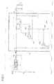
- FIG. 3 is a schematic view illustrating the circuit configuration of a power supply circuit 1.
- the power supply circuit 1 mainly includes a circuit 2 and a switching regulator 10.
- the power supply circuit 1 uses the switching regulator 10 to drop a voltage BATT (ideal value thereof is 14 V) input from a battery 3 and outputs a predetermined voltage VIN (a first specific voltage) (ideal value thereof is 6 V).
- the power supply circuit 1a uses a series regulator 20 of the circuit 2 to drop the voltage VIN, and outputs a predetermined voltage VCC (a second specific voltage) (ideal value thereof is 1.2 V) to a load 4 (for example, a micro computer of an electronic control unit (ECU)).
- ECU electronice control unit
- the voltage VIN is an input voltage which is input from the circuit 2 through a terminal Ta
- the voltage VCC is an output voltage which is output from the circuit 2 through a terminal Tb.
- the ECU may be an engine control ECU for controlling driving of an engine
- the power supply circuit 1 may be used for supplying constant electric power to a micro computer of the ECU.
- each of the switching regulator 10 and the series regulator 20 regulates the voltage input thereto within a range having the input voltage as an upper limit, and outputs the regulated voltage. Therefore, if the input voltage becomes lower than a target output voltage, the output voltage also becomes lower than the target output voltage. In other words, if the voltage BATT of the battery becomes lower than the target output voltage of each regulator, according to the drop of the voltage BATT, the voltage VIN obtained by voltage dropping of the switching regulator 10 and the voltage VCC (the voltage of the load 4) obtained by voltage dropping of the series regulator 20 also become lower than the target voltages.
- the power supply circuit 1 mainly includes the circuit 2 and the switching regulator 10.
- the switching regulator 10 mainly includes a switching circuit unit 101, a coil 102, and a capacitor 103.
- the one end of the switching circuit unit 101 is connected to the battery 3, and the other end thereof is connected to one end of the coil 102 which will be described below. Also, the switching circuit unit 101 is connected to a ground.
- the switching circuit unit 101 converts the voltage BATT into a voltage according to switching control of a switching element (for example, an N-channel metal oxide semiconductor field effect transistor (MOSFET)) provided in the switching circuit unit 101, and outputs the converted voltage.
- a switching element for example, an N-channel metal oxide semiconductor field effect transistor (MOSFET)
- One end of the coil 102 is connected to the other end of the switching circuit unit 101.
- the other end of the coil 102 is connected to one end of the capacitor 103 and the terminal Ta of the circuit 2. Also, the other end of the coil 102 is provided with a feedback loop to output a voltage to the switching circuit unit 101.
- the one end of the capacitor 103 is connected to the other end of the coil 102 and the terminal Ta of the circuit 2.
- the other end of the capacitor 103 is connected to the ground.
- the coil 102 and the capacitor 103 smooth a voltage output from the switching circuit unit 101 and output the voltage VIN to the circuit 2.
- the circuit 2 mainly includes the series regulator 20 and a control circuit 30.
- the series regulator 20 mainly includes a PNP transistor 201, a resistor 202, a resistor 203, an error amplifier 204, a reference power supply 205, an amplifier circuit 206, a buffer 207, a capacitor 208, a constant current source 209, a switch 210, and a resistor 211.
- the emitter of the PNP transistor 201 is connected to the terminal Ta through a signal line L1, and the collector thereof is connected to the terminal Tb through a signal line L2.
- the base thereof is connected to the output terminal of the buffer 207 for transmitting a signal which is output from the output terminal of the error amplifier 204.
- the resistor 202 and the resistor 203 are connected in series between the signal line L2 and the ground.
- the connection point of the resistor 202 and the resistor 203 is connected to the non-inverting input terminal of the error amplifier 204.
- the error amplifier 204 has the non-inverting input terminal, an inverting input terminal, and the output terminal.
- the non-inverting input terminal is connected to the connection point of the resistor 202 and the resistor 203, and a voltage which is obtained by dividing the voltage VCC with the resistor 202 and the resistor 203 is input to the non-inverting input terminal.
- the inverting input terminal is connected to the reference power supply 205.
- the output terminal is connected to the input terminal of the amplifier circuit 206, the other end of the capacitor 208, and one end of the switch 210.
- the voltage value of the reference power supply 205 is 1.0V, for example.
- the error amplifier 204 is an arithmetic circuit. In the series regulator 20, the error amplifier 204 may be substituted by an arithmetic circuit other than the error amplifier 204 as long as the arithmetic circuit has the same function as that of the error amplifier 204.
- One end of the reference power supply 205 is connected to the inverting input terminal of the error amplifier 204 and the other end of the reference power supply 205 is connected to the ground.
- the input terminal of the amplifier circuit 206 is connected to the output terminal of the error amplifier 204 and the output terminal of the amplifier circuit 206 is connected to the input terminal of the buffer 207.
- the amplifier circuit 206 amplifies the signal level of a signal output from the output terminal of the error amplifier 204. For example, the amplifier circuit 206 amplifies the signal level by a factor of 8.
- the input terminal of the buffer 207 is connected to the output terminal of the amplifier circuit 206 and the output terminal of the buffer 207 is connected to the base of the PNP transistor 201.
- the buffer 207 outputs the signal output from the output terminal of the amplifier circuit 206 to the base of the PNP transistor 201 without attenuating the signal level of the signal.
- the one end of the capacitor 208 is connected to the signal line L2 and the other end of the capacitor 208 is connected to the one end of the switch 210 and the output terminal of the error amplifier 204.
- the capacitor 208 has a function of phase compensation for stabilizing the phase of the signal output from the output terminal of the error amplifier 204, and accumulates electric charge of a current flowing from the constant current source 209 which will be described below.
- the capacitor 208 is provided inside the circuit 2, whereby it is possible to reduce the board area of the circuit.
- the constant current source 209 is connected to the other end of the switch 210.
- the voltage of the constant current source 209 is, for example, 6V, and makes a predetermined current flow continuously.
- the one end of the switch 210 is connected to the output terminal of the error amplifier 204 and the one end of the capacitor 208 and the other end of the switch 210 is connected to the constant current source 209.
- the switch 210 is switched to any one of an ON state and an OFF state on the basis of a signal from the output terminal of a comparator 303 of the control circuit 30.
- the resistor 211 is a resistor (a leak cut resistor) for making the potentials of the base and the emitter of the PNP transistor 201 equal to each other when no signal from the output terminal of the buffer 207 is input to the base of the PNP transistor 201, that is, when the signal from the output terminal of the error amplifier 204 is not input to the base of the PNP transistor 201.
- the control circuit 30 mainly includes a resistor 301, a resistor 302, the comparator 303, and a reference power supply 304.
- the resistor 301 and the resistor 302 are connected in series between the signal line L1 and the ground.
- the connection point of the resistor 301 and the resistor 302 is connected to the inverting input terminal of the comparator 303.
- the control circuit 30 has a function of controlling the ON or OFF state of the switch 210 according to the voltage value of the voltage VIN, thereby adjusting an amount of electric charge to be accumulated in the capacitor 208.
- the inverting input terminal of the comparator 303 is connected to the connection point of the resistor 301 and the resistor 302.
- the non-inverting input terminal of the comparator 303 is connected to the reference power supply 304.
- the output terminal of the comparator 303 outputs a high-level signal or a low-level signal to the switch 210 and the switch 210 is configured to be switched to any one of the ON state and the OFF state according to the high-level signal or low-level signal input thereto.
- One end of the reference power supply 304 is connected to the non-inverting input terminal of the comparator 303 and the other end of the reference power supply 304 is connected to the ground.
- the voltage value of the reference power supply 304 is 1.25V, for example.
- the switch 210 is switched to the ON state or the OFF state according to the high-level signal or the low-level signal from the output terminal of the comparator 303.
- the switch 210 in a case where the high-level signal is output from the output terminal of the comparator 303, the switch 210 is switched to the ON state such that the current of the constant current source 209 flows into the capacitor 208. As a result, the electric charge of the capacitor 208 increases.
- the switch 210 is switched to the OFF state such that the electric charge accumulated in the capacitor 208 flows into the error amplifier 204. As a result, the electric charge of the capacitor 208 decreases.
- the terminal Tb of the circuit 2 of the power supply circuit 1 is connected to one end of a capacitor 41 and one end of the load 4.
- the capacitor 41 and the load 4 are provided outside the power supply circuit 1.
- the other end of the capacitor 41 and the other end of the load 4 are connected to the ground.
- the capacitor 41 removes the high frequency components of a voltage which is output from the terminal Tb of the circuit 2, and accumulates the electric charge of a current flowing from the circuit 2 through the terminal Tb.
- the capacitor 208 and the capacitor 41 may be ceramic capacitors, electrolytic capacitors, or the like.
- the switching regulator 10 drops the voltage BATT input from the battery 3, and outputs the voltage VIN.
- the voltage VIN output from the switching regulator 10 is input to the circuit 2 through the terminal Ta.
- the voltage VIN input to the circuit 2 is divided with the resistor 301 and the resistor 302.
- the comparator 303 compares a first voltage which is the divided voltage with a first reference voltage which is the voltage value of the reference power supply 304. Since the operation of the series regulator 20 differs depends on the result of the comparison, when the ideal value of the voltage VIN is set to 6V, a case where the voltage VIN is less than 6V and a case where the voltage VIN is 6V or greater will be separately described.
- the comparator 303 outputs the high-level signal from the output terminal thereof. Then, according to the high-level signal output from the output terminal, the switch 210 becomes the ON state and the electric charge of the current flowing from the constant current source 209 is accumulated in the capacitor 208 through the switch 210.
- a signal for turning off the PNP transistor 201 is input from the output terminal of the error amplifier 204 to the input terminal of the amplifier circuit 206. Then, the signal for turning off the PNP transistor is output from the output terminal of the amplifier circuit 206 to the base of the PNP transistor 201 through the buffer 207, whereby the PNP transistor 201 becomes the OFF state.
- the decreasing rate of the voltage of the capacitor 41 becomes relatively small. In other words, the decreasing rate of the voltage VCC of the power supply circuit 1 becomes smaller than the decreasing rate of the voltage VCC of the power supply circuit 1a according to the related art.
- the comparator 303 outputs the low-level signal from the output terminal thereof. Then, according to the low-level signal output from the output terminal, the switch 210 becomes the OFF state, and a current corresponding to the electric charge accumulated in the capacitor 208 flows into the output terminal of the error amplifier 204. Since the switch 210 is in the OFF state, the electric charge of the constant current source 209 does not flow into the capacitor 208.
- the increasing rate of the voltage of the capacitor 41 becomes relatively small.
- the increasing rate of the voltage VCC of the power supply circuit 1 becomes smaller than the increasing rate of the voltage VCC of the power supply circuit 1a according to the related art.
- the changing rate of the voltage VCC of the power supply circuit 1 becomes smaller than the changing rate of the voltage VCC of the power supply circuit 1a according to the related art. Therefore, it is possible to prevent oscillation of the output voltage VCC of the power supply circuit 1, thereby ensuring the stability of the voltage value.
- the upper chart of FIG. 4 is a chart illustrating a change with time in the voltage value of the voltage BATT of the battery 3 with a graph line VB.
- the lower chart of FIG. 4 is a chart illustrating changes with time in the voltage VIN and the voltage VCC with a graph line VI and a graph line VC.
- the vertical axes represent voltage (V)
- the horizontal axes represent time ( ⁇ sec).
- a higher threshold value of a plurality of threshold values corresponding to the first reference voltage of the comparator 303 is referred to as a first threshold value th
- a lower threshold value of the plurality of threshold values corresponding to the first reference voltage of the comparator 303 is referred to as a second threshold value tw.
- the switch 210 when the value of the graph line VI is equal to or greater than the first threshold value th, the switch 210 becomes the ON state, and when the value of the graph line VI is lower than the second threshold value tw, the switch becomes the OFF state.
- the first threshold value th is 3.2V
- the second threshold value tw is 3V.
- the voltage value of the voltage BATT of the battery 3 decreases at a predetermined slope.
- the graph line VB represents 3V, and this represents that the voltage BATT is 3V.
- the value of the graph line VI of the voltage VIN also becomes 3V. In other words, the voltage value of the voltage VIN becomes equal to or less than the second threshold value tw.
- the switch 210 becomes the OFF state
- the amplifier circuit 206 stops operation thereof
- the PNP transistor 201 becomes the OFF state
- any current does not flow between the emitter and the collector of the PNP transistor 201.
- the series regulator 20 stops outputting.
- the voltage VCC becomes a voltage value less than a voltage of 1.2V with which the load 4 is operable. If the series regulator 20 stops outputting, any current does not flow from the terminal Ta to the terminal Tb. Then, due to self-induced electromotive force generated in the coil 102 of the switching regulator 10 shown in FIG. 3 , the voltage temporarily rises so that the current continuously flows in the same direction. As a result, despite the decrease of the voltage value of the battery 3, the value of the voltage VIN increases.
- the PNP transistor 201 becomes the ON state.
- electric charge flows between the emitter and collector of the PNP transistor 201, and the value of the output voltage VCC of the power supply circuit 1 increases.
- the graph line VI of FIG. 4 representing the voltage VIN is compared to the graph line VIa of FIG. 2 representing the voltage VIN, it can be recognized that the changing rate of the graph line VI of FIG. 4 is smaller than the changing rate of the graph line Via of FIG. 2 .
- the timing when the value of the voltage VIN becomes equal to or greater than the first threshold value th is the time t2 later than the time t2a.
- the voltage value of the voltage VCC changes according to increase or decrease in the electric charge of the capacitor 208.
- a difference in potential between the emitter and the collector of the PNP transistor 201 is set to be relatively small by accumulating electric charge in the capacitor 208 while the PNP transistor 201 is in the OFF state, it is possible to reduce the changing rate of the voltage VCC of the power supply circuit 1 shown in FIG. 3 , as compared to the changing rate of the voltage VCC of the power supply circuit 1a according to the related art shown in FIG. 1 . Therefore, the time intervals of switching of the PNP transistor 201 between the ON state and the OFF state in the power supply circuit 1 according to this embodiment are longer than those of the power supply circuit 1a according to the related art.
- the amplitude of the voltage VIN of the power supply circuit 1 becomes smaller and the period of the voltage VIN becomes longer, as compared with the graph line VIa in FIG. 2 .
- a change per unit time in the voltage value of the voltage VIN becomes smaller as compared to the related art.
- the amplitude of the voltage VCC of the power supply circuit 1 becomes smaller and the period of the voltage VCC becomes longer, as compared to the graph line VCa in FIG. 2 .
- a period from the time t1 to a time t3 which is one period of the graph line VI and the graph line VC corresponding to the voltage VIN and the voltage VCC of the power supply circuit 1 is longer than a period from the time t1a to the time t3a regarding the power supply circuit 1a.
- the amplitudes of the graph line VI and the graph line VC are also smaller as compared with the graph line VIa and the graph line VCa. As such, from the time t1, the values of the graph line VI and the graph line VC change according to changes of the voltage VIN and the voltage VCC.
- the power supply circuit 1 can output the output voltage corresponding to the target voltage to the load 4, and in a case of the transition from the IG-ON state to the IG-OFF state, that is, in a case where the input voltage decreases with time, it is possible to prevent oscillation of the output voltage.
- the capacitor 208 shown in FIG. 3 is provided inside the circuit 2 of the power supply circuit 1.
- the capacitor 208 may be provided outside the circuit 2.
- the capacitance of the capacitor due to the relation with the other internal elements of the circuit 2.
- the capacitance in the case of providing the capacitor 208 inside the circuit 2 is 10 pF
- the capacitance in the case of providing the capacitor 208 outside the circuit 2 it is possible to set the capacitance to 0.1 ⁇ F which is 10 4 times of 10 pF.
- the capacitor 208 is provided outside the circuit 2, it is possible to reduce the number of internal components of the circuit 2.
- the power supply circuit 1 shown in FIG. 3 includes the switching regulator 10 having the coil 102 at the input stage of the circuit 2.
- a series regulator may be provided at the input stage of the circuit 2 to drop the voltage of the battery 3 to the target voltage (the voltage VIN).
- the target voltage for example, 1.2V
- the PNP transistor 201 is employed as a switching element.
- another switching element for example, an NPN transistor.
- the voltage values of the voltages are mere an example. As long as the characteristics of the input and output voltages of each regulator are kept, other voltage values may be used.
- the constant current source 209 is provided inside the series regulator 20. However, it may be provided outside the series regulator 20.
Landscapes
- Engineering & Computer Science (AREA)
- Power Engineering (AREA)
- Continuous-Control Power Sources That Use Transistors (AREA)
- Dc-Dc Converters (AREA)
Abstract
Description
- The disclosure of Japanese Patent Application No.
2012-102789 filed on April 27, 2012 - The present invention relates to a power supply circuit for dropping a voltage.
- A vehicle has various electronic devices (for example, an electronic control unit (ECU)) to which a battery supplies electric power. Also, the vehicle has a power supply circuit which drops an input voltage from the battery and output the dropped voltage to the electronic devices.
FIG. 1 is a schematic view illustrating the circuit configuration of a power supply circuit 1a according to the related art. - The power supply circuit 1a mainly includes a
switching regulator 10 and a circuit 2a including aseries regulator 20a and acontrol circuit 30a. The power supply circuit 1a uses theswitching regulator 10 to drop a voltage BATT (ideal value thereof is 14V) input from abattery 3 and outputs a predetermined voltage VIN (ideal value thereof is 6V). Then, the power supply circuit 1a uses theseries regulator 20a of the circuit 2a to drop the voltage VIN, and outputs a predetermined voltage VCC (ideal value thereof is 1.2V) to a load 4 (for example, a micro computer of an ECU). - Also, each of the
switching regulator 10 and theseries regulator 20a regulates the voltage input thereto within a range having the input voltage as an upper limit, and outputs the regulated voltage. Therefore, if the input voltage becomes lower than a target output voltage, the output voltage also becomes lower than the target output voltage. - In other words, if the voltage BATT of the battery becomes lower than the target output voltage of each regulator, according to the drop of the voltage BATT, the voltage VIN obtained by voltage dropping of the
switching regulator 10 and the voltage VCC (the voltage of the load 4) obtained by voltage dropping of theseries regulator 20a also become lower than the target voltages. All of voltages to be described in this specification are DC voltages. - Next, the circuit operation of the power supply circuit 1a will be described in detail. The
switching regulator 10 drops the voltage BATT input from thebattery 3 to the voltage VIN, and outputs the voltage VIN. The voltage VIN output from theswitching regulator 10 is input to the circuit 2a through a terminal Ta. Then, thecontrol circuit 30a of the circuit 2a divides the input voltage VIN with resistors. Acomparator 303 compares this divided voltage (hereinafter, referred to as a 'first voltage') with a reference voltage (hereinafter, referred to as a 'first reference voltage'). Subsequently, according to the result of the comparison, thecontrol circuit 30a turns on or off aswitch 305 for switching the operation state of anamplifier circuit 206 of theseries regulator 20a. - The first reference voltage of the
comparator 303 has a plurality of threshold values due to hysteresis, but may have one threshold value. Here, the operation of the power supply circuit 1a differs depending on whether the voltage VIN has a voltage value equal to or greater than a predetermined voltage (for example, 6V or greater) or the voltage VIN has a voltage value less than the predetermined voltage (for example, less than 6V). In other words, the output of thecomparator 303 changes depending on whether the first voltage has a voltage value equal to or greater than the first reference voltage or the first voltage is less than the first reference voltage. According to the change in the output of thecomparator 303, theswitch 305 is turned on or off, resulting in the difference in the operation of the power supply circuit 1a. For this reason, the two cases will be separately described below. - In the case where the voltage VIN is 6V or greater, that is, in a case where the first voltage is equal to or greater than the first reference voltage, according to the output of the
comparator 303, theswitch 305 becomes an ON state. As a result, theamplifier circuit 206 of theseries regulator 20a becomes an operable state. - Further, the output voltage of the
series regulator 20a is divided with resistors, and this divided voltage (hereinafter, referred to as a 'second voltage') is input to a non-inverting input terminal of anerror amplifier 204. Then, theerror amplifier 204 compares the second voltage with a reference voltage (hereinafter, referred to as a 'second reference voltage'). In a case where the second voltage has a voltage value less than the second reference voltage, theerror amplifier 204 drives aPNP transistor 201 to raise the second voltage. In other words, thePNP transistor 201 becomes an ON state, a current flows between the emitter and the collector of the PNP transistor, and the potential of the voltage VCC increases. As a result, for example, even when the voltage value of the voltage BATT of thebattery 3 decreases temporarily and thus the output voltage of theseries regulator 20a drops, the power supply circuit 1a can output an optimal voltage for the operation of the load 4. - The
error amplifier 204 operates to stop thePNP transistor 201 to drop the second voltage in the case where the second voltage has a voltage value equal to or greater than the second reference voltage. In other words, thePNP transistor 201 becomes an OFF state, any current does not flow between the emitter and the collector of thePNP transistor 201, and the potential of the voltage VCC drops. As a result, for example, even when the voltage value of the voltage BATT of thebattery 3 increases temporarily and the output of theseries regulator 20a rises, the power supply circuit 1a can output an optimal voltage for the operation of the load 4. - In the case where the voltage VIN is less than 6V, that is, in a case where the first voltage is less than the first reference voltage, according to the output of the
comparator 303, theswitch 305 becomes an OFF state. As a result, theamplifier circuit 206 of the series regulator stops. Therefore, a signal output from an output terminal of theerror amplifier 204 is not input to the base of thePNP transistor 201, thePNP transistor 201 becomes the OFF state, and any current does not flow between the emitter and the collector of thePNP transistor 201. Like this, in the case where the voltage VIN is less than 6V, thepower supply circuit 1 operates to stop the operation of the load 4. Therefore, the voltage value of the output voltage VCC of the power supply circuit 1a drops to be lower than a voltage value for making the operation of the load 4 possible. Japanese Patent Application Publication No.2010-224825A - In the above-mentioned power supply circuit 1a, however, in a case where a vehicle transitions from an IG-ON state to an IG-OFF state, that is, in a case where the voltage value of the voltage BATT of the
battery 3 drops at a predetermined rate every unit time, the voltage value of the voltage VCC to be output to the load 4 oscillates to be unstable. Here, the oscillation means that the voltage value oscillates at a constant frequency while being equal to or greater than a constant value. - Specifically, the oscillation means that the voltage value of the voltage VIN changes due to a drop of the voltage BATT and the voltage value of the voltage VCC changes according to the change of the voltage value of the voltage VIN.
FIG. 2 is charts illustrating changes with time in the voltage BATT, the voltage VIN, and the voltage VCC. Hereinafter, the detailed description will be provided with reference toFIG. 2 . - The upper chart of
FIG. 2 is a chart illustrating the change with time in the voltage value of the voltage BATT of thebattery 3 with a graph line VB. Further, the lower chart ofFIG. 2 is a chart illustrating the changes with time in the voltage values of the voltage VIN and the voltage VCC with a graph line VIa and a graph line VCa, respectively. In the upper and lower charts ofFIG. 2 , the vertical axes represent voltage (V), and the horizontal axes represent time (µsec). - Also, in the lower chart of
FIG. 2 , a higher threshold value of a plurality of threshold values corresponding to the first reference voltage of thecomparator 303 is referred to as a first threshold value th, and a lower threshold value of the plurality of threshold values corresponding to the first reference voltage of thecomparator 303 is referred to as a second threshold value tw. In other words, when the value of the graph line VIa is equal to or greater than the first threshold value th, theswitch 305 becomes the ON state, and when the value of the graph line VIa is lower than the second threshold value tw, theswitch 305 becomes the OFF state. In the lower chart ofFIG. 2 , the first threshold value th is 3.2V, and the second threshold value tw is 3V. - First, in a case where a vehicle transitions from an IG-ON state to an IG-OFF state, as shown by the graph line VB in the upper chart of
FIG. 2 , the voltage value of the voltage BATT of thebattery 3 decreases at a predetermined slope. At a time t1a, the graph line VB is 3V, and this represents that the voltage BATT is 3V. In this case, since the voltage BATT is less than the target output voltage value of theswitching regulator 10, the value of the graph line VIa of the voltage VIN also becomes 3V. In other words, the voltage value of the voltage VIN becomes equal to or less than the second threshold value tw. As a result, theswitch 305 becomes the OFF state, theamplifier circuit 206 stops, thePNP transistor 201 becomes the OFF state, and any current does not flow between the emitter and the collector of thePNP transistor 201. In other words, theseries regulator 20a stops operation thereof. - Further, if the voltage value of the voltage VIN becomes equal to or less than 3V, as shown by the graph line VCa, the voltage value of the voltage VCC also decreases. As a result, the voltage VCC becomes a voltage value less than a voltage of 1.2V with which the load 4 is operable.
- Here, if the
series regulator 20a stops outputting, any current does not flow from the terminal Ta to a terminal Tb. Then, due to self-induced electromotive force generated in acoil 102 of theswitching regulator 10 shown inFIG. 1 , the voltage temporarily rises so that a current continuously flows in the same direction. As a result, despite the decrease of the voltage value of thebattery 3, the value of the voltage VIN increases. Then, when the value of the voltage VIN becomes equal to or greater than the first threshold value th at a time t2a, theamplifier circuit 206 becomes operable, and thePNP transistor 201 becomes the ON state. As a result, a relatively large amount of electric charge flows between the emitter and collector of thePNP transistor 201, and the value of the output voltage VCC of the power supply circuit 1a increases at a predetermined or greater slope. - Subsequently, according to a large amount of current output from the power supply circuit 1a, the voltage value of the voltage VIN decreases at a predetermined or greater slope. Then, the value of the voltage VCC becomes 3V or less at a time t3a within a relatively short time (for example, at a frequency of 20 µsec). As a result, the
amplifier circuit 206 stops operation thereof, and thePNP transistor 201 becomes the OFF state and thus any current does not flow between the emitter and the collector of thePNP transistor 201. - When the voltage value of the voltage VIN becomes 3V or less, the value of the voltage VCC also decreases. As a result, the voltage VCC becomes less than the voltage (1.2 V) for operating the load 4. In this case, since the
series regulator 20a stops outputting, the value of the voltage VIN which is input from the switchingregulator 10 to the circuit 2a increases due to the characteristics of thecoil 102 of the switchingregulator 10 or the like, as described above. Then, when the value of the voltage VIN becomes the first threshold value th or greater at a time t4a, theamplifier circuit 206 becomes operable, and thePNP transistor 201 becomes the ON state. As a result, a relatively large amount of current flows between the emitter and collector of thePNP transistor 201, and thus the voltage value of the output voltage VCC of the power supply circuit 1a increases at a predetermined or greater slope. When the vehicle transitions to the IG-OFF state, these relatively sudden increases and decreases in voltage value are repeated, whereby the voltage VIN oscillates and the voltage VCC also oscillates. As a result, the voltage for operating the load 4 may become an unstable state. - It is therefore an object of the present invention to ensure the stability of the voltage value of an output voltage.
- In order to achieve the above object, according to an aspect of the embodiments of the present invention, there is provided a power supply circuit comprising: a switching regulator configured to drop a battery voltage to a first specific voltage; a series regulator including a switching element and a capacitor connected at an output stage of the switching element, the series regulator configured to drop the first specific voltage to a second specific voltage, and output the second specific voltage; and a control circuit configured to adjust an amount of electric charge to be accumulated in the capacitor according to a voltage value of the first specific voltage.
- The control circuit may be configured to perform control for increasing the electric charge of the capacitor in a case where the first specific voltage is lower than a predetermined voltage, and perform control for decreasing the electric charge of the capacitor in a case where the first specific voltage is higher than a predetermined voltage.
- The series regulator may further include an arithmetic circuit configured to output a signal for controlling an operation state of the switching element according to a voltage value of the second specific voltage, and the control by the control circuit for increasing the electric charge may be control for accumulating electric charge from a constant current source in the capacitor, and the control by the control circuit for decreasing the electric charge may be control for causing the electric charge accumulated in the capacitor to flow into the arithmetic circuit.
- According to the present invention, an amount of electric charge to be accumulated in the capacitor is regulated according to the voltage value of the first specific voltage. Therefore, it is possible to prevent oscillation of the main voltage of the power supply circuit, thereby ensuring the stability of the voltage value. Also, according to the present invention, it is possible to adjust the change state of the output voltage according to a change in the capacitance of the capacitor, and it is possible to prevent oscillation of the output voltage of the power supply circuit, thereby ensuring the stability of the voltage value.
- Further, according to the present invention, it is possible to adjust the change state of the output voltage according to a change in the amount of electric charge flowing into the constant current source, and it is possible to prevent oscillation of the output voltage of the power supply circuit, thereby ensuring the stability of the voltage value.
- In the accompanying drawings:
-
FIG. 1 is a schematic view illustrating the circuit configuration of a power supply circuit according to the related art; -
FIG. 2 is charts illustrating changes with time in a voltage BATT, a voltage VIN, and a voltage VCC according to the related art; -
FIG. 3 is a schematic view illustrating the circuit configuration of a power supply circuit according to an embodiment of the present invention; and -
FIG. 4 is charts illustrating changes with time in a voltage BATT, a voltage VIN, and a voltage VCC according to the embodiment of the present invention. - Hereinafter, an embodiment of the present invention will be described with reference to the accompanying drawings. The following embodiment is merely exemplary and is not intended to limit the technical scope of the present invention of this application.
-
FIG. 3 is a schematic view illustrating the circuit configuration of apower supply circuit 1. Thepower supply circuit 1 mainly includes a circuit 2 and aswitching regulator 10. Thepower supply circuit 1 uses theswitching regulator 10 to drop a voltage BATT (ideal value thereof is 14 V) input from abattery 3 and outputs a predetermined voltage VIN (a first specific voltage) (ideal value thereof is 6 V). Then, the power supply circuit 1a uses aseries regulator 20 of the circuit 2 to drop the voltage VIN, and outputs a predetermined voltage VCC (a second specific voltage) (ideal value thereof is 1.2 V) to a load 4 (for example, a micro computer of an electronic control unit (ECU)). The voltage VIN is an input voltage which is input from the circuit 2 through a terminal Ta, and the voltage VCC is an output voltage which is output from the circuit 2 through a terminal Tb. Further, the ECU may be an engine control ECU for controlling driving of an engine, and thepower supply circuit 1 may be used for supplying constant electric power to a micro computer of the ECU. - Also, each of the switching
regulator 10 and theseries regulator 20 regulates the voltage input thereto within a range having the input voltage as an upper limit, and outputs the regulated voltage. Therefore, if the input voltage becomes lower than a target output voltage, the output voltage also becomes lower than the target output voltage. In other words, if the voltage BATT of the battery becomes lower than the target output voltage of each regulator, according to the drop of the voltage BATT, the voltage VIN obtained by voltage dropping of the switchingregulator 10 and the voltage VCC (the voltage of the load 4) obtained by voltage dropping of theseries regulator 20 also become lower than the target voltages. - Next, the configuration of the
power supply circuit 1 will be described in detail. Thepower supply circuit 1 mainly includes the circuit 2 and the switchingregulator 10. The switchingregulator 10 mainly includes aswitching circuit unit 101, acoil 102, and acapacitor 103. - The one end of the
switching circuit unit 101 is connected to thebattery 3, and the other end thereof is connected to one end of thecoil 102 which will be described below. Also, the switchingcircuit unit 101 is connected to a ground. The switchingcircuit unit 101 converts the voltage BATT into a voltage according to switching control of a switching element (for example, an N-channel metal oxide semiconductor field effect transistor (MOSFET)) provided in theswitching circuit unit 101, and outputs the converted voltage. - One end of the
coil 102 is connected to the other end of theswitching circuit unit 101. The other end of thecoil 102 is connected to one end of thecapacitor 103 and the terminal Ta of the circuit 2. Also, the other end of thecoil 102 is provided with a feedback loop to output a voltage to theswitching circuit unit 101. - The one end of the
capacitor 103 is connected to the other end of thecoil 102 and the terminal Ta of the circuit 2. The other end of thecapacitor 103 is connected to the ground. - The
coil 102 and thecapacitor 103 smooth a voltage output from the switchingcircuit unit 101 and output the voltage VIN to the circuit 2. - The circuit 2 mainly includes the
series regulator 20 and acontrol circuit 30. Theseries regulator 20 mainly includes aPNP transistor 201, aresistor 202, aresistor 203, anerror amplifier 204, areference power supply 205, anamplifier circuit 206, abuffer 207, acapacitor 208, a constantcurrent source 209, aswitch 210, and aresistor 211. - The emitter of the
PNP transistor 201 is connected to the terminal Ta through a signal line L1, and the collector thereof is connected to the terminal Tb through a signal line L2. The base thereof is connected to the output terminal of thebuffer 207 for transmitting a signal which is output from the output terminal of theerror amplifier 204. - The
resistor 202 and theresistor 203 are connected in series between the signal line L2 and the ground. The connection point of theresistor 202 and theresistor 203 is connected to the non-inverting input terminal of theerror amplifier 204. - The
error amplifier 204 has the non-inverting input terminal, an inverting input terminal, and the output terminal. The non-inverting input terminal is connected to the connection point of theresistor 202 and theresistor 203, and a voltage which is obtained by dividing the voltage VCC with theresistor 202 and theresistor 203 is input to the non-inverting input terminal. The inverting input terminal is connected to thereference power supply 205. The output terminal is connected to the input terminal of theamplifier circuit 206, the other end of thecapacitor 208, and one end of theswitch 210. The voltage value of thereference power supply 205 is 1.0V, for example. Theerror amplifier 204 is an arithmetic circuit. In theseries regulator 20, theerror amplifier 204 may be substituted by an arithmetic circuit other than theerror amplifier 204 as long as the arithmetic circuit has the same function as that of theerror amplifier 204. - One end of the
reference power supply 205 is connected to the inverting input terminal of theerror amplifier 204 and the other end of thereference power supply 205 is connected to the ground. - The input terminal of the
amplifier circuit 206 is connected to the output terminal of theerror amplifier 204 and the output terminal of theamplifier circuit 206 is connected to the input terminal of thebuffer 207. Theamplifier circuit 206 amplifies the signal level of a signal output from the output terminal of theerror amplifier 204. For example, theamplifier circuit 206 amplifies the signal level by a factor of 8. - The input terminal of the
buffer 207 is connected to the output terminal of theamplifier circuit 206 and the output terminal of thebuffer 207 is connected to the base of thePNP transistor 201. Thebuffer 207 outputs the signal output from the output terminal of theamplifier circuit 206 to the base of thePNP transistor 201 without attenuating the signal level of the signal. - The one end of the
capacitor 208 is connected to the signal line L2 and the other end of thecapacitor 208 is connected to the one end of theswitch 210 and the output terminal of theerror amplifier 204. Thecapacitor 208 has a function of phase compensation for stabilizing the phase of the signal output from the output terminal of theerror amplifier 204, and accumulates electric charge of a current flowing from the constantcurrent source 209 which will be described below. As shown inFIG. 3 , thecapacitor 208 is provided inside the circuit 2, whereby it is possible to reduce the board area of the circuit. - The constant
current source 209 is connected to the other end of theswitch 210. The voltage of the constantcurrent source 209 is, for example, 6V, and makes a predetermined current flow continuously. - The one end of the
switch 210 is connected to the output terminal of theerror amplifier 204 and the one end of thecapacitor 208 and the other end of theswitch 210 is connected to the constantcurrent source 209. Theswitch 210 is switched to any one of an ON state and an OFF state on the basis of a signal from the output terminal of acomparator 303 of thecontrol circuit 30. - The
resistor 211 is a resistor (a leak cut resistor) for making the potentials of the base and the emitter of thePNP transistor 201 equal to each other when no signal from the output terminal of thebuffer 207 is input to the base of thePNP transistor 201, that is, when the signal from the output terminal of theerror amplifier 204 is not input to the base of thePNP transistor 201. - The
control circuit 30 mainly includes a resistor 301, aresistor 302, thecomparator 303, and areference power supply 304. The resistor 301 and theresistor 302 are connected in series between the signal line L1 and the ground. The connection point of the resistor 301 and theresistor 302 is connected to the inverting input terminal of thecomparator 303. Thecontrol circuit 30 has a function of controlling the ON or OFF state of theswitch 210 according to the voltage value of the voltage VIN, thereby adjusting an amount of electric charge to be accumulated in thecapacitor 208. - The inverting input terminal of the
comparator 303 is connected to the connection point of the resistor 301 and theresistor 302. The non-inverting input terminal of thecomparator 303 is connected to thereference power supply 304. The output terminal of thecomparator 303 outputs a high-level signal or a low-level signal to theswitch 210 and theswitch 210 is configured to be switched to any one of the ON state and the OFF state according to the high-level signal or low-level signal input thereto. - One end of the
reference power supply 304 is connected to the non-inverting input terminal of thecomparator 303 and the other end of thereference power supply 304 is connected to the ground. The voltage value of thereference power supply 304 is 1.25V, for example. - The
switch 210 is switched to the ON state or the OFF state according to the high-level signal or the low-level signal from the output terminal of thecomparator 303. In other words, in a case where the high-level signal is output from the output terminal of thecomparator 303, theswitch 210 is switched to the ON state such that the current of the constantcurrent source 209 flows into thecapacitor 208. As a result, the electric charge of thecapacitor 208 increases. In a case where the low-level signal is output from the output terminal of thecomparator 303, theswitch 210 is switched to the OFF state such that the electric charge accumulated in thecapacitor 208 flows into theerror amplifier 204. As a result, the electric charge of thecapacitor 208 decreases. - The terminal Tb of the circuit 2 of the
power supply circuit 1 is connected to one end of acapacitor 41 and one end of the load 4. Thecapacitor 41 and the load 4 are provided outside thepower supply circuit 1. The other end of thecapacitor 41 and the other end of the load 4 are connected to the ground. Thecapacitor 41 removes the high frequency components of a voltage which is output from the terminal Tb of the circuit 2, and accumulates the electric charge of a current flowing from the circuit 2 through the terminal Tb. Thecapacitor 208 and thecapacitor 41 may be ceramic capacitors, electrolytic capacitors, or the like. - Next, the operation of the
power supply circuit 1 will be described. The switchingregulator 10 drops the voltage BATT input from thebattery 3, and outputs the voltage VIN. The voltage VIN output from the switchingregulator 10 is input to the circuit 2 through the terminal Ta. Then, the voltage VIN input to the circuit 2 is divided with the resistor 301 and theresistor 302. Thecomparator 303 compares a first voltage which is the divided voltage with a first reference voltage which is the voltage value of thereference power supply 304. Since the operation of theseries regulator 20 differs depends on the result of the comparison, when the ideal value of the voltage VIN is set to 6V, a case where the voltage VIN is less than 6V and a case where the voltage VIN is 6V or greater will be separately described. - In the case where the voltage VIN is less than 6V, the first voltage obtained by divising the voltage with the resistor 301 and the
resistor 302 has a voltage value less than the first reference voltage. Therefore, thecomparator 303 outputs the high-level signal from the output terminal thereof. Then, according to the high-level signal output from the output terminal, theswitch 210 becomes the ON state and the electric charge of the current flowing from the constantcurrent source 209 is accumulated in thecapacitor 208 through theswitch 210. In this case, since the voltage of the output terminal of theerror amplifier 204 rises, a signal for turning off thePNP transistor 201 is input from the output terminal of theerror amplifier 204 to the input terminal of theamplifier circuit 206. Then, the signal for turning off the PNP transistor is output from the output terminal of theamplifier circuit 206 to the base of thePNP transistor 201 through thebuffer 207, whereby thePNP transistor 201 becomes the OFF state. - As a result, any current does not flow between the emitter and the collector of the
PNP transistor 201, and the electric charge from the constantcurrent source 209 is accumulated in thecapacitor 208. Therefore, the decreasing rate of the voltage of thecapacitor 41 becomes relatively small. In other words, the decreasing rate of the voltage VCC of thepower supply circuit 1 becomes smaller than the decreasing rate of the voltage VCC of the power supply circuit 1a according to the related art. - In the case where the voltage VIN is 6V or greater, the first voltage obtained by dividing the voltage with the resistor 301 and the
resistor 302 is equal to or greater than the first reference voltage. Therefore, thecomparator 303 outputs the low-level signal from the output terminal thereof. Then, according to the low-level signal output from the output terminal, theswitch 210 becomes the OFF state, and a current corresponding to the electric charge accumulated in thecapacitor 208 flows into the output terminal of theerror amplifier 204. Since theswitch 210 is in the OFF state, the electric charge of the constantcurrent source 209 does not flow into thecapacitor 208. In this case, since the voltage of the output terminal of theerror amplifier 204 decreases, a signal input from the output terminal of theerror amplifier 204 to the input terminal of theamplifier circuit 206 becomes a signal for driving thePNP transistor 201. Then, the signal for driving thePNP transistor 201 is output from the output terminal of theamplifier circuit 206 to the base of thePNP transistor 201 through thebuffer 207, whereby thePNP transistor 201 becomes the ON state. Therefore, a current flows between the emitter and the collector of thePNP transistor 201, whereby the voltage value of the voltage VCC to be output from the terminal Tb of the circuit 2 rises. - As a result, the increasing rate of the voltage of the
capacitor 41 becomes relatively small. In other words, the increasing rate of the voltage VCC of thepower supply circuit 1 becomes smaller than the increasing rate of the voltage VCC of the power supply circuit 1a according to the related art. As such, the changing rate of the voltage VCC of thepower supply circuit 1 becomes smaller than the changing rate of the voltage VCC of the power supply circuit 1a according to the related art. Therefore, it is possible to prevent oscillation of the output voltage VCC of thepower supply circuit 1, thereby ensuring the stability of the voltage value. Further, by changing any one factor of the capacitance of thecapacitor 208, the amount of current of the constantcurrent source 209, and the amount of current to flow into theerror amplifier 204 to arbitrary value in advance, it is possible to adjust an amount of change per unit time in the voltage value of the voltage VCC. As a result, it is possible to prevent oscillation of the voltage VCC, thereby ensure the stability of the voltage value. - Change with time in the voltage VIN and the voltage VCC will be described be described with reference to
FIG. 4 . The upper chart ofFIG. 4 is a chart illustrating a change with time in the voltage value of the voltage BATT of thebattery 3 with a graph line VB. Also, the lower chart ofFIG. 4 is a chart illustrating changes with time in the voltage VIN and the voltage VCC with a graph line VI and a graph line VC. In the upper and lower charts ofFIG. 4 , the vertical axes represent voltage (V), and the horizontal axes represent time (µsec). - In the lower chart of
FIG. 4 , a higher threshold value of a plurality of threshold values corresponding to the first reference voltage of thecomparator 303 is referred to as a first threshold value th, and a lower threshold value of the plurality of threshold values corresponding to the first reference voltage of thecomparator 303 is referred to as a second threshold value tw. In other words, when the value of the graph line VI is equal to or greater than the first threshold value th, theswitch 210 becomes the ON state, and when the value of the graph line VI is lower than the second threshold value tw, the switch becomes the OFF state. In the lower chart ofFIG. 4 , the first threshold value th is 3.2V, and the second threshold value tw is 3V. - First, in a case where a vehicle transitions from an IG-ON state to an IG-OFF state, as shown by the graph line VB in the upper chart of
FIG. 4 , the voltage value of the voltage BATT of thebattery 3 decreases at a predetermined slope. At a time t1, the graph line VB represents 3V, and this represents that the voltage BATT is 3V. In this case, since the voltage BATT is less than the target voltage value of the switchingregulator 10, the value of the graph line VI of the voltage VIN also becomes 3V. In other words, the voltage value of the voltage VIN becomes equal to or less than the second threshold value tw. As a result, theswitch 210 becomes the OFF state, theamplifier circuit 206 stops operation thereof, thePNP transistor 201 becomes the OFF state, and any current does not flow between the emitter and the collector of thePNP transistor 201. In other words, theseries regulator 20 stops outputting. - Further, if the voltage value of the voltage VIN becomes equal to or less than 3V, as shown by the graph line VC, the voltage VCC also decreases. As a result, the voltage VCC becomes a voltage value less than a voltage of 1.2V with which the load 4 is operable. If the
series regulator 20 stops outputting, any current does not flow from the terminal Ta to the terminal Tb. Then, due to self-induced electromotive force generated in thecoil 102 of the switchingregulator 10 shown inFIG. 3 , the voltage temporarily rises so that the current continuously flows in the same direction. As a result, despite the decrease of the voltage value of thebattery 3, the value of the voltage VIN increases. - Then, when the value of the voltage VIN becomes equal to or greater than the first threshold value th at a time t2, the
PNP transistor 201 becomes the ON state. As a result, electric charge flows between the emitter and collector of thePNP transistor 201, and the value of the output voltage VCC of thepower supply circuit 1 increases. As the graph line VI ofFIG. 4 representing the voltage VIN is compared to the graph line VIa ofFIG. 2 representing the voltage VIN, it can be recognized that the changing rate of the graph line VI ofFIG. 4 is smaller than the changing rate of the graph line Via ofFIG. 2 . In other words, the timing when the value of the voltage VIN becomes equal to or greater than the first threshold value th is the time t2 later than the time t2a. - The voltage value of the voltage VCC changes according to increase or decrease in the electric charge of the
capacitor 208. In this embodiment, since a difference in potential between the emitter and the collector of thePNP transistor 201 is set to be relatively small by accumulating electric charge in thecapacitor 208 while thePNP transistor 201 is in the OFF state, it is possible to reduce the changing rate of the voltage VCC of thepower supply circuit 1 shown inFIG. 3 , as compared to the changing rate of the voltage VCC of the power supply circuit 1a according to the related art shown inFIG. 1 . Therefore, the time intervals of switching of thePNP transistor 201 between the ON state and the OFF state in thepower supply circuit 1 according to this embodiment are longer than those of the power supply circuit 1a according to the related art. - As a result, as shown by the graph line VI in
FIG. 4 , the amplitude of the voltage VIN of thepower supply circuit 1 becomes smaller and the period of the voltage VIN becomes longer, as compared with the graph line VIa inFIG. 2 . In other words, a change per unit time in the voltage value of the voltage VIN becomes smaller as compared to the related art. Further, as shown by the graph line VC inFIG. 4 , the amplitude of the voltage VCC of thepower supply circuit 1 becomes smaller and the period of the voltage VCC becomes longer, as compared to the graph line VCa inFIG. 2 . - In other words, a period from the time t1 to a time t3 which is one period of the graph line VI and the graph line VC corresponding to the voltage VIN and the voltage VCC of the
power supply circuit 1 is longer than a period from the time t1a to the time t3a regarding the power supply circuit 1a. The amplitudes of the graph line VI and the graph line VC are also smaller as compared with the graph line VIa and the graph line VCa. As such, from the time t1, the values of the graph line VI and the graph line VC change according to changes of the voltage VIN and the voltage VCC. - Thereafter, as a state where the voltage value of the voltage VCC corresponding to the graph line VC is smaller than a voltage value with which the load 4 is operable continues, the operation of the load 4 completely stops. Therefore, it is possible to prevent oscillation of the output voltage VCC of the
power supply circuit 1, thereby ensuring the stability of the voltage value. Like this, according to the configuration of this embodiment, in a case of the IG-ON state, thepower supply circuit 1 can output the output voltage corresponding to the target voltage to the load 4, and in a case of the transition from the IG-ON state to the IG-OFF state, that is, in a case where the input voltage decreases with time, it is possible to prevent oscillation of the output voltage. - Although the embodiment of the present invention has been described above, the present invention is not limited to the above-mentioned embodiment but can be variously modified. Hereinafter, these modifications will be described. The above-mentioned embodiment and the following modifications can be appropriately combined.
- In the above-mentioned embodiment, the
capacitor 208 shown inFIG. 3 is provided inside the circuit 2 of thepower supply circuit 1. However, thecapacitor 208 may be provided outside the circuit 2. In the case where the capacitor is provided inside the circuit 2, there are limits on the capacitance of the capacitor due to the relation with the other internal elements of the circuit 2. However, in the case of providing the capacitor outside the circuit 2, since there is no influence of the other internal elements of the circuit 2, it is possible to set the capacitance to be larger than that in the case of providing the capacitor inside the circuit 2. Specifically, for example, assuming that the capacitance in the case of providing thecapacitor 208 inside the circuit 2 is 10 pF, in the case of providing thecapacitor 208 outside the circuit 2, it is possible to set the capacitance to 0.1 µF which is 104 times of 10 pF. Also, if thecapacitor 208 is provided outside the circuit 2, it is possible to reduce the number of internal components of the circuit 2. - In the above-mentioned embodiment, the
power supply circuit 1 shown inFIG. 3 includes the switchingregulator 10 having thecoil 102 at the input stage of the circuit 2. However, it is not necessarily needed to provide theswitching regulator 10 having thecoil 102. For example, a series regulator may be provided at the input stage of the circuit 2 to drop the voltage of thebattery 3 to the target voltage (the voltage VIN). In this case, it is possible to prevent the rising voltage value of the voltage VCC per unit time from becoming a relatively large voltage value to exceed the target voltage (for example, 1.2V) (to overshoot), and to make a change per unit time in the voltage when the voltage VCC rises a relatively small value. - Also, in the above-mentioned embodiment, the
PNP transistor 201 is employed as a switching element. However, it is possible to change the circuit configuration and substitute thePNP transistor 201 by another switching element (for example, an NPN transistor). - Also, in the above-mentioned embodiment, the voltage values of the voltages (the input voltage and the output voltage) corresponding to the driving of each regulator described with reference to
FIG. 3 are mere an example. As long as the characteristics of the input and output voltages of each regulator are kept, other voltage values may be used. - Also, in the above-mentioned embodiment, the constant
current source 209 is provided inside theseries regulator 20. However, it may be provided outside theseries regulator 20.
Claims (3)
- A power supply circuit comprising:a switching regulator configured to drop a battery voltage to a first specific voltage;a series regulator including a switching element and a capacitor connected at an output stage of the switching element, the series regulator configured to drop the first specific voltage to a second specific voltage, and output the second specific voltage; anda control circuit configured to adjust an amount of electric charge to be accumulated in the capacitor according to a voltage value of the first specific voltage.
- The power supply circuit according to claim 1, wherein the control circuit is configured to perform control for increasing the electric charge of the capacitor in a case where the first specific voltage is lower than a predetermined voltage, and perform control for decreasing the electric charge of the capacitor in a case where the first specific voltage is higher than a predetermined voltage.
- The power supply circuit according to claim 2,
wherein the series regulator further includes an arithmetic circuit configured to output a signal for controlling an operation state of the switching element according to a voltage value of the second specific voltage, and
wherein the control by the control circuit for increasing the electric charge is control for accumulating electric charge from a constant current source in the capacitor, and the control by the control circuit for decreasing the electric charge is control for causing the electric charge accumulated in the capacitor to flow into the arithmetic circuit.
Applications Claiming Priority (1)
| Application Number | Priority Date | Filing Date | Title |
|---|---|---|---|
| JP2012102789A JP6038481B2 (en) | 2012-04-27 | 2012-04-27 | Power circuit |
Publications (3)
| Publication Number | Publication Date |
|---|---|
| EP2658108A2 true EP2658108A2 (en) | 2013-10-30 |
| EP2658108A3 EP2658108A3 (en) | 2017-06-28 |
| EP2658108B1 EP2658108B1 (en) | 2020-12-02 |
Family
ID=48087466
Family Applications (1)
| Application Number | Title | Priority Date | Filing Date |
|---|---|---|---|
| EP13163847.0A Active EP2658108B1 (en) | 2012-04-27 | 2013-04-16 | Power supply circuit |
Country Status (3)
| Country | Link |
|---|---|
| US (1) | US9054579B2 (en) |
| EP (1) | EP2658108B1 (en) |
| JP (1) | JP6038481B2 (en) |
Families Citing this family (3)
| Publication number | Priority date | Publication date | Assignee | Title |
|---|---|---|---|---|
| US9178506B2 (en) | 2012-09-20 | 2015-11-03 | Crydom, Inc. | High speed charge control for power switching devices |
| US10001794B2 (en) * | 2014-09-30 | 2018-06-19 | Analog Devices, Inc. | Soft start circuit and method for DC-DC voltage regulator |
| CN111064176B (en) * | 2019-11-28 | 2021-02-02 | 中国地质大学(武汉) | Digital control turn-off and self-starting low-power consumption voltage monitoring circuit |
Citations (1)
| Publication number | Priority date | Publication date | Assignee | Title |
|---|---|---|---|---|
| JP2010224825A (en) | 2009-03-23 | 2010-10-07 | Toshiba Corp | Semiconductor integrated circuit |
Family Cites Families (4)
| Publication number | Priority date | Publication date | Assignee | Title |
|---|---|---|---|---|
| JPH07325633A (en) * | 1994-06-01 | 1995-12-12 | Matsushita Electric Ind Co Ltd | Power supply system switching circuit for battery-powered equipment |
| JP2000242345A (en) * | 1999-02-17 | 2000-09-08 | Texas Instr Inc <Ti> | Voltage drop limiting device and operating method |
| JP4479797B2 (en) * | 2008-01-23 | 2010-06-09 | 株式会社デンソー | Electronic control unit |
| TWM406872U (en) * | 2011-02-24 | 2011-07-01 | Richtek Technology Corp | Power management circuit |
-
2012
- 2012-04-27 JP JP2012102789A patent/JP6038481B2/en active Active
-
2013
- 2013-04-11 US US13/860,829 patent/US9054579B2/en active Active
- 2013-04-16 EP EP13163847.0A patent/EP2658108B1/en active Active
Patent Citations (1)
| Publication number | Priority date | Publication date | Assignee | Title |
|---|---|---|---|---|
| JP2010224825A (en) | 2009-03-23 | 2010-10-07 | Toshiba Corp | Semiconductor integrated circuit |
Also Published As
| Publication number | Publication date |
|---|---|
| EP2658108B1 (en) | 2020-12-02 |
| EP2658108A3 (en) | 2017-06-28 |
| US9054579B2 (en) | 2015-06-09 |
| JP6038481B2 (en) | 2016-12-07 |
| JP2013232055A (en) | 2013-11-14 |
| US20130285635A1 (en) | 2013-10-31 |
Similar Documents
| Publication | Publication Date | Title |
|---|---|---|
| US9785165B2 (en) | Voltage regulator with improved line regulation transient response | |
| US7049879B2 (en) | Power supply circuit with control of rise characteristics of output voltage | |
| JP5577829B2 (en) | Power supply device, control circuit, and control method for power supply device | |
| US8525580B2 (en) | Semiconductor circuit and constant voltage regulator employing same | |
| EP2973971B1 (en) | Systems and methods for 100 percent duty cycle in switching regulators | |
| US10193449B2 (en) | Buck voltage converter | |
| JP4666345B2 (en) | Charge pump circuit | |
| JP2007049845A (en) | Switching regulator | |
| CN1879285B (en) | DC/DC Converter | |
| KR20150075034A (en) | Switching regulator and electronic apparatus | |
| JP2017107551A (en) | Power regulator | |
| JP2020156215A (en) | Switching power supply | |
| US9054579B2 (en) | Power supply circuit | |
| US10830798B2 (en) | Voltage variation detection circuit, semiconductor integrated circuit, and vehicle | |
| US7453251B1 (en) | Voltage tracking reference for a power regulator | |
| US20140241017A1 (en) | Input circuit and power supply circuit | |
| KR101774601B1 (en) | Switching regulator control circuit and switching regulator | |
| JP2010015471A (en) | Regulator apparatus, and electronic apparatus provided with the same | |
| EP2713492B1 (en) | Power Conversion Arrangement and Method for Power Conversion | |
| US20240356435A1 (en) | Voltage boost circuit and sensor device | |
| CN202978705U (en) | DC/DC output circuit | |
| JP7504050B2 (en) | Shunt Regulator | |
| JP2004318339A (en) | Dropper type regulator and power supply device using the same | |
| JP2009118692A (en) | DC-DC converter | |
| KR102065576B1 (en) | Switching dc-dc converter, circuit and method to convert voltage thereof |
Legal Events
| Date | Code | Title | Description |
|---|---|---|---|
| PUAI | Public reference made under article 153(3) epc to a published international application that has entered the european phase |
Free format text: ORIGINAL CODE: 0009012 |
|
| AK | Designated contracting states |
Kind code of ref document: A2 Designated state(s): AL AT BE BG CH CY CZ DE DK EE ES FI FR GB GR HR HU IE IS IT LI LT LU LV MC MK MT NL NO PL PT RO RS SE SI SK SM TR |
|
| AX | Request for extension of the european patent |
Extension state: BA ME |
|
| PUAL | Search report despatched |
Free format text: ORIGINAL CODE: 0009013 |
|
| AK | Designated contracting states |
Kind code of ref document: A3 Designated state(s): AL AT BE BG CH CY CZ DE DK EE ES FI FR GB GR HR HU IE IS IT LI LT LU LV MC MK MT NL NO PL PT RO RS SE SI SK SM TR |
|
| AX | Request for extension of the european patent |
Extension state: BA ME |
|
| RIC1 | Information provided on ipc code assigned before grant |
Ipc: H02M 3/156 20060101AFI20170522BHEP |
|
| STAA | Information on the status of an ep patent application or granted ep patent |
Free format text: STATUS: REQUEST FOR EXAMINATION WAS MADE |
|
| 17P | Request for examination filed |
Effective date: 20171220 |
|
| RBV | Designated contracting states (corrected) |
Designated state(s): AL AT BE BG CH CY CZ DE DK EE ES FI FR GB GR HR HU IE IS IT LI LT LU LV MC MK MT NL NO PL PT RO RS SE SI SK SM TR |
|
| STAA | Information on the status of an ep patent application or granted ep patent |
Free format text: STATUS: EXAMINATION IS IN PROGRESS |
|
| 17Q | First examination report despatched |
Effective date: 20191209 |
|
| GRAP | Despatch of communication of intention to grant a patent |
Free format text: ORIGINAL CODE: EPIDOSNIGR1 |
|
| STAA | Information on the status of an ep patent application or granted ep patent |
Free format text: STATUS: GRANT OF PATENT IS INTENDED |
|
| INTG | Intention to grant announced |
Effective date: 20200728 |
|
| RIN1 | Information on inventor provided before grant (corrected) |
Inventor name: SHIMIZU, YUICHIRO |
|
| GRAS | Grant fee paid |
Free format text: ORIGINAL CODE: EPIDOSNIGR3 |
|
| GRAA | (expected) grant |
Free format text: ORIGINAL CODE: 0009210 |
|
| STAA | Information on the status of an ep patent application or granted ep patent |
Free format text: STATUS: THE PATENT HAS BEEN GRANTED |
|
| AK | Designated contracting states |
Kind code of ref document: B1 Designated state(s): AL AT BE BG CH CY CZ DE DK EE ES FI FR GB GR HR HU IE IS IT LI LT LU LV MC MK MT NL NO PL PT RO RS SE SI SK SM TR |
|
| REG | Reference to a national code |
Ref country code: GB Ref legal event code: FG4D |
|
| REG | Reference to a national code |
Ref country code: AT Ref legal event code: REF Ref document number: 1342006 Country of ref document: AT Kind code of ref document: T Effective date: 20201215 Ref country code: CH Ref legal event code: EP |
|
| REG | Reference to a national code |
Ref country code: DE Ref legal event code: R096 Ref document number: 602013074402 Country of ref document: DE |
|
| REG | Reference to a national code |
Ref country code: IE Ref legal event code: FG4D |
|
| REG | Reference to a national code |
Ref country code: DE Ref legal event code: R082 Ref document number: 602013074402 Country of ref document: DE Representative=s name: HL KEMPNER PATENTANWAELTE, SOLICITORS (ENGLAND, DE Ref country code: DE Ref legal event code: R082 Ref document number: 602013074402 Country of ref document: DE Representative=s name: HL KEMPNER PATENTANWALT, RECHTSANWALT, SOLICIT, DE Ref country code: DE Ref legal event code: R082 Ref document number: 602013074402 Country of ref document: DE Representative=s name: HL KEMPNER PARTG MBB, DE |
|
| PG25 | Lapsed in a contracting state [announced via postgrant information from national office to epo] |
Ref country code: GR Free format text: LAPSE BECAUSE OF FAILURE TO SUBMIT A TRANSLATION OF THE DESCRIPTION OR TO PAY THE FEE WITHIN THE PRESCRIBED TIME-LIMIT Effective date: 20210303 Ref country code: FI Free format text: LAPSE BECAUSE OF FAILURE TO SUBMIT A TRANSLATION OF THE DESCRIPTION OR TO PAY THE FEE WITHIN THE PRESCRIBED TIME-LIMIT Effective date: 20201202 Ref country code: RS Free format text: LAPSE BECAUSE OF FAILURE TO SUBMIT A TRANSLATION OF THE DESCRIPTION OR TO PAY THE FEE WITHIN THE PRESCRIBED TIME-LIMIT Effective date: 20201202 Ref country code: NO Free format text: LAPSE BECAUSE OF FAILURE TO SUBMIT A TRANSLATION OF THE DESCRIPTION OR TO PAY THE FEE WITHIN THE PRESCRIBED TIME-LIMIT Effective date: 20210302 |
|
| REG | Reference to a national code |
Ref country code: NL Ref legal event code: MP Effective date: 20201202 |
|
| REG | Reference to a national code |
Ref country code: AT Ref legal event code: MK05 Ref document number: 1342006 Country of ref document: AT Kind code of ref document: T Effective date: 20201202 |
|
| PG25 | Lapsed in a contracting state [announced via postgrant information from national office to epo] |
Ref country code: SE Free format text: LAPSE BECAUSE OF FAILURE TO SUBMIT A TRANSLATION OF THE DESCRIPTION OR TO PAY THE FEE WITHIN THE PRESCRIBED TIME-LIMIT Effective date: 20201202 Ref country code: LV Free format text: LAPSE BECAUSE OF FAILURE TO SUBMIT A TRANSLATION OF THE DESCRIPTION OR TO PAY THE FEE WITHIN THE PRESCRIBED TIME-LIMIT Effective date: 20201202 Ref country code: PL Free format text: LAPSE BECAUSE OF FAILURE TO SUBMIT A TRANSLATION OF THE DESCRIPTION OR TO PAY THE FEE WITHIN THE PRESCRIBED TIME-LIMIT Effective date: 20201202 Ref country code: BG Free format text: LAPSE BECAUSE OF FAILURE TO SUBMIT A TRANSLATION OF THE DESCRIPTION OR TO PAY THE FEE WITHIN THE PRESCRIBED TIME-LIMIT Effective date: 20210302 |
|
| PG25 | Lapsed in a contracting state [announced via postgrant information from national office to epo] |
Ref country code: NL Free format text: LAPSE BECAUSE OF FAILURE TO SUBMIT A TRANSLATION OF THE DESCRIPTION OR TO PAY THE FEE WITHIN THE PRESCRIBED TIME-LIMIT Effective date: 20201202 Ref country code: HR Free format text: LAPSE BECAUSE OF FAILURE TO SUBMIT A TRANSLATION OF THE DESCRIPTION OR TO PAY THE FEE WITHIN THE PRESCRIBED TIME-LIMIT Effective date: 20201202 |
|
| REG | Reference to a national code |
Ref country code: LT Ref legal event code: MG9D |
|
| PG25 | Lapsed in a contracting state [announced via postgrant information from national office to epo] |
Ref country code: PT Free format text: LAPSE BECAUSE OF FAILURE TO SUBMIT A TRANSLATION OF THE DESCRIPTION OR TO PAY THE FEE WITHIN THE PRESCRIBED TIME-LIMIT Effective date: 20210405 Ref country code: RO Free format text: LAPSE BECAUSE OF FAILURE TO SUBMIT A TRANSLATION OF THE DESCRIPTION OR TO PAY THE FEE WITHIN THE PRESCRIBED TIME-LIMIT Effective date: 20201202 Ref country code: SK Free format text: LAPSE BECAUSE OF FAILURE TO SUBMIT A TRANSLATION OF THE DESCRIPTION OR TO PAY THE FEE WITHIN THE PRESCRIBED TIME-LIMIT Effective date: 20201202 Ref country code: LT Free format text: LAPSE BECAUSE OF FAILURE TO SUBMIT A TRANSLATION OF THE DESCRIPTION OR TO PAY THE FEE WITHIN THE PRESCRIBED TIME-LIMIT Effective date: 20201202 Ref country code: CZ Free format text: LAPSE BECAUSE OF FAILURE TO SUBMIT A TRANSLATION OF THE DESCRIPTION OR TO PAY THE FEE WITHIN THE PRESCRIBED TIME-LIMIT Effective date: 20201202 Ref country code: EE Free format text: LAPSE BECAUSE OF FAILURE TO SUBMIT A TRANSLATION OF THE DESCRIPTION OR TO PAY THE FEE WITHIN THE PRESCRIBED TIME-LIMIT Effective date: 20201202 Ref country code: SM Free format text: LAPSE BECAUSE OF FAILURE TO SUBMIT A TRANSLATION OF THE DESCRIPTION OR TO PAY THE FEE WITHIN THE PRESCRIBED TIME-LIMIT Effective date: 20201202 |
|
| PG25 | Lapsed in a contracting state [announced via postgrant information from national office to epo] |
Ref country code: AT Free format text: LAPSE BECAUSE OF FAILURE TO SUBMIT A TRANSLATION OF THE DESCRIPTION OR TO PAY THE FEE WITHIN THE PRESCRIBED TIME-LIMIT Effective date: 20201202 |
|
| REG | Reference to a national code |
Ref country code: DE Ref legal event code: R097 Ref document number: 602013074402 Country of ref document: DE |
|
| PG25 | Lapsed in a contracting state [announced via postgrant information from national office to epo] |
Ref country code: IS Free format text: LAPSE BECAUSE OF FAILURE TO SUBMIT A TRANSLATION OF THE DESCRIPTION OR TO PAY THE FEE WITHIN THE PRESCRIBED TIME-LIMIT Effective date: 20210402 |
|
| PLBE | No opposition filed within time limit |
Free format text: ORIGINAL CODE: 0009261 |
|
| STAA | Information on the status of an ep patent application or granted ep patent |
Free format text: STATUS: NO OPPOSITION FILED WITHIN TIME LIMIT |
|
| PG25 | Lapsed in a contracting state [announced via postgrant information from national office to epo] |
Ref country code: IT Free format text: LAPSE BECAUSE OF FAILURE TO SUBMIT A TRANSLATION OF THE DESCRIPTION OR TO PAY THE FEE WITHIN THE PRESCRIBED TIME-LIMIT Effective date: 20201202 Ref country code: AL Free format text: LAPSE BECAUSE OF FAILURE TO SUBMIT A TRANSLATION OF THE DESCRIPTION OR TO PAY THE FEE WITHIN THE PRESCRIBED TIME-LIMIT Effective date: 20201202 |
|
| 26N | No opposition filed |
Effective date: 20210903 |
|
| PG25 | Lapsed in a contracting state [announced via postgrant information from national office to epo] |
Ref country code: SI Free format text: LAPSE BECAUSE OF FAILURE TO SUBMIT A TRANSLATION OF THE DESCRIPTION OR TO PAY THE FEE WITHIN THE PRESCRIBED TIME-LIMIT Effective date: 20201202 Ref country code: MC Free format text: LAPSE BECAUSE OF FAILURE TO SUBMIT A TRANSLATION OF THE DESCRIPTION OR TO PAY THE FEE WITHIN THE PRESCRIBED TIME-LIMIT Effective date: 20201202 Ref country code: ES Free format text: LAPSE BECAUSE OF FAILURE TO SUBMIT A TRANSLATION OF THE DESCRIPTION OR TO PAY THE FEE WITHIN THE PRESCRIBED TIME-LIMIT Effective date: 20201202 Ref country code: DK Free format text: LAPSE BECAUSE OF FAILURE TO SUBMIT A TRANSLATION OF THE DESCRIPTION OR TO PAY THE FEE WITHIN THE PRESCRIBED TIME-LIMIT Effective date: 20201202 |
|
| GBPC | Gb: european patent ceased through non-payment of renewal fee |
Effective date: 20210416 |
|
| PG25 | Lapsed in a contracting state [announced via postgrant information from national office to epo] |
Ref country code: LU Free format text: LAPSE BECAUSE OF NON-PAYMENT OF DUE FEES Effective date: 20210416 |
|
| REG | Reference to a national code |
Ref country code: BE Ref legal event code: MM Effective date: 20210430 |
|
| PG25 | Lapsed in a contracting state [announced via postgrant information from national office to epo] |
Ref country code: LI Free format text: LAPSE BECAUSE OF NON-PAYMENT OF DUE FEES Effective date: 20210430 Ref country code: CH Free format text: LAPSE BECAUSE OF NON-PAYMENT OF DUE FEES Effective date: 20210430 Ref country code: FR Free format text: LAPSE BECAUSE OF NON-PAYMENT OF DUE FEES Effective date: 20210430 Ref country code: GB Free format text: LAPSE BECAUSE OF NON-PAYMENT OF DUE FEES Effective date: 20210416 |
|
| PG25 | Lapsed in a contracting state [announced via postgrant information from national office to epo] |
Ref country code: IE Free format text: LAPSE BECAUSE OF NON-PAYMENT OF DUE FEES Effective date: 20210416 |
|
| PG25 | Lapsed in a contracting state [announced via postgrant information from national office to epo] |
Ref country code: IS Free format text: LAPSE BECAUSE OF FAILURE TO SUBMIT A TRANSLATION OF THE DESCRIPTION OR TO PAY THE FEE WITHIN THE PRESCRIBED TIME-LIMIT Effective date: 20210402 |
|
| PG25 | Lapsed in a contracting state [announced via postgrant information from national office to epo] |
Ref country code: BE Free format text: LAPSE BECAUSE OF NON-PAYMENT OF DUE FEES Effective date: 20210430 |
|
| PG25 | Lapsed in a contracting state [announced via postgrant information from national office to epo] |
Ref country code: HU Free format text: LAPSE BECAUSE OF FAILURE TO SUBMIT A TRANSLATION OF THE DESCRIPTION OR TO PAY THE FEE WITHIN THE PRESCRIBED TIME-LIMIT; INVALID AB INITIO Effective date: 20130416 |
|
| PG25 | Lapsed in a contracting state [announced via postgrant information from national office to epo] |
Ref country code: CY Free format text: LAPSE BECAUSE OF FAILURE TO SUBMIT A TRANSLATION OF THE DESCRIPTION OR TO PAY THE FEE WITHIN THE PRESCRIBED TIME-LIMIT Effective date: 20201202 |
|
| PG25 | Lapsed in a contracting state [announced via postgrant information from national office to epo] |
Ref country code: MK Free format text: LAPSE BECAUSE OF FAILURE TO SUBMIT A TRANSLATION OF THE DESCRIPTION OR TO PAY THE FEE WITHIN THE PRESCRIBED TIME-LIMIT Effective date: 20201202 |
|
| PG25 | Lapsed in a contracting state [announced via postgrant information from national office to epo] |
Ref country code: MT Free format text: LAPSE BECAUSE OF FAILURE TO SUBMIT A TRANSLATION OF THE DESCRIPTION OR TO PAY THE FEE WITHIN THE PRESCRIBED TIME-LIMIT Effective date: 20201202 |
|
| PGFP | Annual fee paid to national office [announced via postgrant information from national office to epo] |
Ref country code: DE Payment date: 20250422 Year of fee payment: 13 |
|
| PG25 | Lapsed in a contracting state [announced via postgrant information from national office to epo] |
Ref country code: TR Free format text: LAPSE BECAUSE OF FAILURE TO SUBMIT A TRANSLATION OF THE DESCRIPTION OR TO PAY THE FEE WITHIN THE PRESCRIBED TIME-LIMIT Effective date: 20201202 |