EP2657814A2 - Touch screen driver - Google Patents
Touch screen driver Download PDFInfo
- Publication number
- EP2657814A2 EP2657814A2 EP13001980.5A EP13001980A EP2657814A2 EP 2657814 A2 EP2657814 A2 EP 2657814A2 EP 13001980 A EP13001980 A EP 13001980A EP 2657814 A2 EP2657814 A2 EP 2657814A2
- Authority
- EP
- European Patent Office
- Prior art keywords
- touch
- lines
- integrated circuit
- touch screen
- raw data
- Prior art date
- Legal status (The legal status is an assumption and is not a legal conclusion. Google has not performed a legal analysis and makes no representation as to the accuracy of the status listed.)
- Granted
Links
Images






Classifications
-
- G—PHYSICS
- G06—COMPUTING OR CALCULATING; COUNTING
- G06F—ELECTRIC DIGITAL DATA PROCESSING
- G06F3/00—Input arrangements for transferring data to be processed into a form capable of being handled by the computer; Output arrangements for transferring data from processing unit to output unit, e.g. interface arrangements
- G06F3/01—Input arrangements or combined input and output arrangements for interaction between user and computer
- G06F3/03—Arrangements for converting the position or the displacement of a member into a coded form
- G06F3/041—Digitisers, e.g. for touch screens or touch pads, characterised by the transducing means
- G06F3/0416—Control or interface arrangements specially adapted for digitisers
- G06F3/04166—Details of scanning methods, e.g. sampling time, grouping of sub areas or time sharing with display driving
-
- G—PHYSICS
- G06—COMPUTING OR CALCULATING; COUNTING
- G06F—ELECTRIC DIGITAL DATA PROCESSING
- G06F3/00—Input arrangements for transferring data to be processed into a form capable of being handled by the computer; Output arrangements for transferring data from processing unit to output unit, e.g. interface arrangements
- G06F3/01—Input arrangements or combined input and output arrangements for interaction between user and computer
- G06F3/03—Arrangements for converting the position or the displacement of a member into a coded form
- G06F3/041—Digitisers, e.g. for touch screens or touch pads, characterised by the transducing means
-
- G—PHYSICS
- G06—COMPUTING OR CALCULATING; COUNTING
- G06F—ELECTRIC DIGITAL DATA PROCESSING
- G06F3/00—Input arrangements for transferring data to be processed into a form capable of being handled by the computer; Output arrangements for transferring data from processing unit to output unit, e.g. interface arrangements
- G06F3/01—Input arrangements or combined input and output arrangements for interaction between user and computer
- G06F3/03—Arrangements for converting the position or the displacement of a member into a coded form
- G06F3/041—Digitisers, e.g. for touch screens or touch pads, characterised by the transducing means
- G06F3/0416—Control or interface arrangements specially adapted for digitisers
-
- G—PHYSICS
- G06—COMPUTING OR CALCULATING; COUNTING
- G06F—ELECTRIC DIGITAL DATA PROCESSING
- G06F3/00—Input arrangements for transferring data to be processed into a form capable of being handled by the computer; Output arrangements for transferring data from processing unit to output unit, e.g. interface arrangements
- G06F3/01—Input arrangements or combined input and output arrangements for interaction between user and computer
- G06F3/03—Arrangements for converting the position or the displacement of a member into a coded form
- G06F3/041—Digitisers, e.g. for touch screens or touch pads, characterised by the transducing means
- G06F3/0412—Digitisers structurally integrated in a display
-
- G—PHYSICS
- G06—COMPUTING OR CALCULATING; COUNTING
- G06F—ELECTRIC DIGITAL DATA PROCESSING
- G06F3/00—Input arrangements for transferring data to be processed into a form capable of being handled by the computer; Output arrangements for transferring data from processing unit to output unit, e.g. interface arrangements
- G06F3/01—Input arrangements or combined input and output arrangements for interaction between user and computer
- G06F3/03—Arrangements for converting the position or the displacement of a member into a coded form
- G06F3/041—Digitisers, e.g. for touch screens or touch pads, characterised by the transducing means
- G06F3/044—Digitisers, e.g. for touch screens or touch pads, characterised by the transducing means by capacitive means
-
- G—PHYSICS
- G06—COMPUTING OR CALCULATING; COUNTING
- G06F—ELECTRIC DIGITAL DATA PROCESSING
- G06F3/00—Input arrangements for transferring data to be processed into a form capable of being handled by the computer; Output arrangements for transferring data from processing unit to output unit, e.g. interface arrangements
- G06F3/01—Input arrangements or combined input and output arrangements for interaction between user and computer
- G06F3/03—Arrangements for converting the position or the displacement of a member into a coded form
- G06F3/041—Digitisers, e.g. for touch screens or touch pads, characterised by the transducing means
- G06F3/044—Digitisers, e.g. for touch screens or touch pads, characterised by the transducing means by capacitive means
- G06F3/0446—Digitisers, e.g. for touch screens or touch pads, characterised by the transducing means by capacitive means using a grid-like structure of electrodes in at least two directions, e.g. using row and column electrodes
-
- B—PERFORMING OPERATIONS; TRANSPORTING
- B32—LAYERED PRODUCTS
- B32B—LAYERED PRODUCTS, i.e. PRODUCTS BUILT-UP OF STRATA OF FLAT OR NON-FLAT, e.g. CELLULAR OR HONEYCOMB, FORM
- B32B2457/00—Electrical equipment
- B32B2457/20—Displays, e.g. liquid crystal displays, plasma displays
- B32B2457/208—Touch screens
-
- G—PHYSICS
- G06—COMPUTING OR CALCULATING; COUNTING
- G06F—ELECTRIC DIGITAL DATA PROCESSING
- G06F2203/00—Indexing scheme relating to G06F3/00 - G06F3/048
- G06F2203/041—Indexing scheme relating to G06F3/041 - G06F3/045
- G06F2203/04111—Cross over in capacitive digitiser, i.e. details of structures for connecting electrodes of the sensing pattern where the connections cross each other, e.g. bridge structures comprising an insulating layer, or vias through substrate
Definitions
- Embodiments of the invention relate to a touch screen, and more particularly, to a touch screen driver for dividedly driving a touch screen.
- User interface is configured so that people (users) can easily control various electronic devices as they desire.
- Examples of the user interface include a keypad, a keyboard, a mouse, an on-screen display (OSD), and a remote controller having an infrared communication function or a radio frequency (RF) communication function.
- RF radio frequency
- the touch UI has been necessarily used in portable information appliances.
- the touch UI has been implemented by a method for forming a touch screen on the screen of a display device.
- a mutual capacitance touch screen includes Tx lines, Rx lines crossing the Tx lines, and touch sensors formed at crossings of the Tx lines and the Rx lines.
- Each of the touch sensors has a mutual capacitance.
- a touch screen driver for driving the mutual capacitance touch screen supplies a driving signal to the Tx lines, and receives charges of the touch sensors through the Rx lines.
- the touch screen driver senses changes in voltages charged to the touch sensors before and after a touch operation to decide whether or not a conductive material touches the touch screen and to decide a touch position when the conductive material touches the touch screen.
- the touch screen driver is integrated into an integrated circuit called a readout integrated circuit (ROIC) and is connected to the touch screen.
- ROIC readout integrated circuit
- one integrated circuit is connected to one touch screen.
- the integrated circuit includes a Tx channel module, which is connected to the Tx lines and supplies the driving signal to the Tx lines, and an Rx channel module, which is connected to the Rx lines and receives charges of the touch sensors through the Rx lines.
- the integrated circuit has to include Tx channels equal to or greater than the number of Tx lines in the touch screen and Rx channels equal to or greater than the number of Rx lines in the touch screen, so as to sense all of the touch sensors of the touch screen.
- Embodiments of the invention provide a touch screen driver capable of driving a touch screen having a plurality of channels using an integrated circuit having a relatively small number of channels.
- a touch screen driver including a plurality of integrated circuits configured to dividedly drive a touch screen, wherein one of the plurality of integrated circuits, which generates a driving signal to be supplied to Tx lines of the touch screen, transmits a synchronization signal synchronized with the driving signal to other integrated circuit, wherein the other integrated circuit receiving the synchronization signal receives charges of the touch sensors through Rx lines of the touch screen in response to the synchronization signal.
- FIG. 1 is a block diagram of a display device according to an example embodiment of the invention.
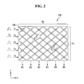
- FIG. 2 is a plane view enlarging a portion of a touch screen shown in FIG. 1 ;
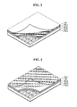
- FIGs. 3 to 5 illustrate various combinations of a touch screen and a display panel according to an example embodiment of the invention
- FIG. 6 illustrates an example of a driving signal supplied to Tx lines
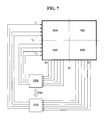
- FIG. 7 illustrates configuration of a touch screen driver according to an example embodiment of the invention
- FIG. 8 is a waveform diagram showing a driving signal and a sync signal generated by a touch screen driver shown in FIG. 7 ;
- FIGs. 9 to 11 illustrate various embodiments of a touch recognition module
- FIG. 12 illustrates another configuration of a touch screen driver according to an example embodiment of the invention.
- FIG. 13 is a waveform diagram showing a driving signal and a sync signal generated by a touch screen driver shown in FIG. 12 .
- a display device includes a display panel DIS, a display driver, a touch screen TSP, a touch screen driver 30, and the like.
- the display device may be implemented based on a flat panel display, such as a liquid crystal display (LCD), a field emission display (FED), a plasma display panel (PDP), an organic light emitting display, and an electrophoresis display (EPD).
- a flat panel display such as a liquid crystal display (LCD), a field emission display (FED), a plasma display panel (PDP), an organic light emitting display, and an electrophoresis display (EPD).
- LCD liquid crystal display
- FED field emission display
- PDP plasma display panel
- EPD electrophoresis display
- the display panel DIS includes a lower substrate GLS2, an upper substrate GLS1, and a liquid crystal layer formed between the lower substrate GLS2 and the upper substrate GLS1.
- the lower substrate GLS2 of the display panel DIS includes a plurality of data lines D1 to Dm, where m is a natural number, a plurality of gate lines (or scan lines) G1 to Gn crossing the data lines D1 to Dm, where n is a natural number, a plurality of thin film transistors (TFTs) formed at crossings of the data lines D1 to Dm and the gate lines G1 to Gn, a plurality of pixel electrodes for charging liquid crystal cells to a data voltage, a plurality of storage capacitors, each of which is connected to the pixel electrode and holds a voltage of the liquid crystal cell, etc.
- the TFTs are turned on in response to a gate pulse (or a scan pulse) from the gate lines G1 to Gn, thereby supplying the voltage from the data lines D1 to Dm to the pixel
- the upper substrate GLS1 of the display panel DIS may include black matrixes, color filters, etc.
- Polarizing plates POL1 and POL2 are respectively attached to the upper and lower substrates GLS1 and GLS2 of the display panel DIS.
- Alignment layers for setting a pre-tilt angle of liquid crystals are respectively formed on the inner surfaces contacting the liquid crystals in the upper and lower substrates GLS1 and GLS2 of the display panel DIS.
- a column spacer is formed between the upper and lower substrates GLS1 and GLS2 of the display panel DIS to keep cell gaps of the liquid crystal cells constant.
- a backlight unit (not shown) may be disposed in the rear of the display panel DIS.
- the backlight unit may be configured as one of an edge type backlight unit and a direct type backlight unit to provide light to the display panel DIS.
- the display panel DIS may be implemented in any known mode including a twisted nematic (TN) mode, a vertical alignment (VA) mode, an in-plane switching (IPS) mode, and a fringe field switching (FFS) mode.
- TN twisted nematic
- VA vertical alignment
- IPS in-plane switching
- FFS fringe field switching
- the display driver includes a data driving circuit 12, a scan driving circuit 14, and a display timing controller 20.
- the display driver writes a video data voltage of an input image to pixels of the display panel DIS.
- the data driving circuit 12 converts digital video data RGB received from the display timing controller 20 into positive and negative analog gamma compensation voltages and outputs the data voltages.
- the data driving circuit 12 supplies the data voltages to the data lines D1 to Dm.
- the scan driving circuit 14 sequentially supplies the gate pulse synchronized with the data voltage to the gate lines G1 to Gn and selects lines of the display panel DIS to which the data voltages are written.
- the display timing controller 20 receives timing signals, such as a vertical sync signal Vsync, a horizontal sync signal Hsync, a data enable signal DE, and a main clock MCLK, from an external host system.
- the display timing controller 20 generates a data timing control signal and a scan timing control signal for respectively controlling operation timing of the data driving circuit 12 and operation timing of the scan driving circuit 14 using the timing signals.
- the data timing control signal includes a source sampling clock SSC, a source output enable signal SOE, a polarity control signal POL, etc.
- the scan timing control signal includes a gate start pulse GSP, a gate shift clock GSC, a gate output enable signal GOE, etc.
- the touch screen TSP may be attached to the upper polarizing plate POL1 of the display panel DIS.
- the touch screen TSP may be formed between the upper polarizing plate POL1 and the upper substrate GLS1.
- touch sensors TSN of the touch screen TSP may be formed on the substrate of the display panel DIS along with a pixel array of the display panel DIS.
- 'PIX' denotes the pixel electrode of the liquid crystal cell.
- the touch screen TSP includes Tx lines T1 to Tj, where 'j' is a positive integer less than n, Rx lines R1 to Ri crossing the Tx lines T1 to Tj, where 'i' is a positive integer less than m, and ixj touch sensors TSN formed at crossings of the Tx lines T1 to Tj and the Rx lines R1 to Ri.
- the touch screen driver 30 supplies a driving signal shown in FIG. 6 to the Tx lines T1 to Tj and receives charges of the touch sensors TSN through the Rx lines R1 to Ri in synchronization with the driving signal to sample voltages of the touch sensors TSN.
- the touch screen driver 30 then converts the sampled voltages of the touch sensors TSN into digital data and generates touch raw data.
- the driving signal supplied to the Tx lines T1 to Tj may be generated as a plurality of driving signal rows.
- the touch screen driver 30 executes a previously determined touch recognition algorithm and analyzes the touch raw data using the touch recognition algorithm.
- the touch screen driver 30 decides touch raw data, which is equal to or greater than a predetermined threshold value, as data of touch (or proximity) input positions and estimates coordinates of the touch (or proximity) input position data.
- the touch recognition algorithm may use any well-known algorithm. Touch coordinate data Txy output from the touch screen driver 30 is transmitted to the host system.
- the host system may be implemented as one of a navigation system, a set-top box, a DVD player, a Blue-ray player, a personal computer (PC), a home theater system, a broadcasting receiver, and a phone system.
- the host system converts data of the input image into a data format suitable to display on the display panel DIS using a scaler embedded therein. Further, the host system runs an application associated with coordinate values of the touch coordinate data Txy received from the touch screen driver 30.
- the touch screen driver 30 includes at least two integrated circuits.
- the integrated circuits are synchronized with each other and dividedly drive the touch screen TSP using a method shown in FIG. 7 or 12 .
- the integrated circuits may dividedly drive the Tx lines T1 to Tj of the touch screen TSP or may dividedly drive the Rx lines R1 to Ri of the touch screen TSP. Alternatively, the integrated circuits may dividedly drive both the Tx lines T1 to Tj and the Rx lines R1 to Ri of the touch screen TSP.
- FIG. 7 illustrates configuration of the touch screen driver 30 according to the embodiment of the invention.
- FIG. 8 is a waveform diagram showing a driving signal and a sync signal generated by the touch screen driver 30 shown in FIG. 7 .
- the touch screen driver 30 includes first and second integrated circuits 200A and 200B for dividedly driving the touch screen TSP which is virtually divided into four parts.
- the touch screen TSP is not physically divided and is divided into first to fourth areas 100A to 100D depending on a connection relationship between the first and second integrated circuits 200A and 200B and the touch screen TSP.
- the first and second areas 100A and 100B are areas belonging to an upper half part of the touch screen TSP.
- the first and second areas 100A and 100B share the Tx lines T1 to Tj/2 formed in the upper half part of the touch screen TSP.
- the first area 100A includes the Rx lines R1 to Ri/2 formed in a left half part of the touch screen TSP, and the second area 100B includes the Rx lines R(i/2+1) to Ri formed in a right half part of the touch screen TSP.
- the third and fourth areas 100C and 100D are areas belonging to a lower half part of the touch screen TSP.
- the third and fourth areas 100C and 100D share the Tx lines T(j/2+1) to Tj formed in the lower half part of the touch screen TSP.
- the third area 100C includes the Rx lines R1 to Ri/2 formed in the left half part of the touch screen TSP and shares the Rx lines R1 to Ri/2 with the first area 100A.
- the fourth area 100D includes the Rx lines R(i/2+1) to Ri formed in the right half part of the touch screen TSP and shares the Rx lines R(i/2+1) to Ri with the second area 100B.
- the first integrated circuit 200A is connected to the Tx lines of a first group and the Rx lines of the first group and senses the touch sensors formed in the first and third areas 100A and 100C of the touch screen TSP.
- the second integrated circuit 200B is connected to the Tx lines of a second group and the Rx lines of the second group and senses the touch sensors formed in the second and fourth areas 100B and 100D of the touch screen TSP.
- Each of the first and second integrated circuits 200A and 200B includes a Tx channel module, an Rx channel module, and a synchronization signal module.
- the Tx channel module supplies a driving signal to the Tx lines. As shown in FIG. 6 , the driving signal may be sequentially supplied to the Tx lines, but is not limited thereto.
- the Rx channel module receives charges of the touch sensors through the Rx lines, samples voltages of the touch sensors, converts the sampled voltages of the touch sensors into digital data, and generates touch raw data.
- the synchronization signal module transmits a synchronization signal SYNC (refer to FIG. 8 ) generated by the first or second integrated circuit generating the driving signal to the second or first integrated circuit and synchronizes sensing operations of the first and second integrated circuits 200A and 200B, thereby preventing a sensing error.
- SYNC synchronization signal
- Tx channels of the first integrated circuit 200A are connected to the Tx lines T(j/2+1) to Tj formed in the lower half part of the touch screen TSP.
- Rx channels of the first integrated circuit 200A are connected to the Rx lines R1 to Ri/2 formed in the left half part of the touch screen TSP.
- the first integrated circuit 200A supplies the driving signal to the Tx lines T(j/2+1) to Tj of the third and fourth areas 100C and 100D and receives the charges of the touch sensors through the Rx lines R1 to Ri/2 of the first and third areas 100A and 100C.
- Tx channels of the second integrated circuit 200B are connected to the Tx lines T1 to Tj/2 formed in the upper half part of the touch screen TSP.
- Rx channels of the second integrated circuit 200B are connected to the Rx lines R(i/2+1) to Ri formed in the right half part of the touch screen TSP.
- the second integrated circuit 200B supplies the driving signal to the Tx lines T1 to Tj/2 of the first and second areas 100A and 100B and receives the charges of the touch sensors through the Rx lines R(i/2+1) to Ri of the second and fourth areas 100B and 100D.
- the first and second integrated circuits 200A and 200B receive charges of the touch sensors through the Rx lines R1 to Ri in synchronization with the driving signal. For this, the first and second integrated circuits 200A and 200B perform bidirectional communication through the synchronization signal SYNC shown in FIG. 8 . Hence, the first and second integrated circuits 200A and 200B are synchronized and driven.
- the synchronization signal SYNC is generated by the integrated circuit supplying the driving signal to the Tx lines and is transmitted to another integrated circuit.
- the second integrated circuit 200B supplies the driving signal to the Tx lines T1 to Tj/2 crossing the first and second areas 100A and 100B of the touch screen TSP.
- the synchronization signal module of the second integrated circuit 200B supplies the synchronization signal SYNC synchronized with the driving signal supplied to the Tx lines T1 to Tj/2 to the first integrated circuit 200A.
- the synchronization signal SYNC may be synchronized with one of a rising edge and a falling edge of the driving signal supplied to the Tx lines T1 to Tj/2 or may be synchronized with both the rising edge and the falling edge of the driving signal supplied to the Tx lines T1 to Tj/2.
- the first integrated circuit 200A receives charges of the touch sensors formed in the first area 100A through the Rx lines R1 to Ri/2, samples voltages of the touch sensors, converts the sampled voltages of the touch sensors into digital data, and generates touch raw data.
- the second integrated circuit 200B receives charges of the touch sensors formed in the second area 100B through the Rx lines R(i/2+1) to Ri, samples voltages of the touch sensors, converts the sampled voltages of the touch sensors into digital data, and generates touch raw data.
- the first integrated circuit 200A supplies the driving signal to the Tx lines T(j/2+1) to Tj crossing the third and fourth areas 100C and 100D of the touch screen TSP.
- the synchronization signal module of the first integrated circuit 200A supplies the synchronization signal SYNC synchronized with a rising edge of the driving signal supplied to the Tx lines T(j/2+1) to Tj to the second integrated circuit 200B.
- the second integrated circuit 200B receives charges of the touch sensors formed in the fourth area 100D through the Rx lines R(i/2+1) to Ri, samples voltages of the touch sensors, converts the sampled voltages of the touch sensors into digital data, and generates touch raw data.
- the first integrated circuit 200A receives charges of the touch sensors formed in the third area 100C through the Rx lines R1 to Ri/2, samples voltages of the touch sensors, converts the sampled voltages of the touch sensors into digital data, and generates touch raw data.
- the touch screen driver 30 further includes a touch recognition module shown in FIGs. 9 to 11 .
- the touch recognition module executes the touch recognition algorithm and analyzes the touch raw data received from each of the first and second integrated circuits 200A and 200B using the touch recognition algorithm to estimate touch (or proximity) input positions. Further, the touch recognition module decides touch raw data, which is equal to or greater than a predetermined threshold value, as data of the touch (or proximity) input positions and estimates coordinates of the touch (or proximity) input position data. Further, the touch recognition module assigns an identification code to each of the touch (or proximity) input positions and recognizes a multi-touch.
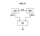
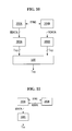
- FIGs. 9 to 11 illustrate various embodiments of the touch recognition module.
- a touch recognition module 300 analyzes touch raw data RDATA received from each of the first and second integrated circuits 200A and 200B and estimates coordinates of touch (or proximity) input positions to output touch coordinate data Txy including coordinate information.
- the touch recognition module 300 may include an offset correction algorithm for correcting a deviation between output offsets of the integrated circuits 200A and 200B.
- the touch recognition module 300 may be embedded in one of the integrated circuits 200A and 200B.
- the touch recognition module includes first and second touch recognition modules 300A and 300B.
- the first touch recognition module 300A analyzes touch raw data RDATA received from the first integrated circuit 200A and estimates coordinates of touch (or proximity) input positions to output touch coordinate data Txy including coordinate information.
- the second touch recognition module 300B analyzes touch raw data RDATA received from the second integrated circuit 200B and estimates coordinates of touch (or proximity) input positions to output touch coordinate data Txy including coordinate information.
- the first touch recognition module 300A may be embedded in the first integrated circuit 200A, and the second touch recognition module 300B may be embedded in the second integrated circuit 200B.
- the touch screen driver 30 further includes a data synchronization module 500 connected to the first and second touch recognition modules 300A and 300B.
- the data synchronization module 500 synchronizes the touch coordinate data Txy output from the first and second touch recognition modules 300A and 300B and transmits the synchronized touch coordinate data Txy to the host system.
- the data synchronization module 500 may include an offset correction algorithm for correcting a deviation between output offsets of the integrated circuits 200A and 200B.
- one of the first and second integrated circuits 200A and 200B may transmit the touch raw data to the other integrated circuit.
- the other integrated circuit receiving the touch raw data from the one integrated circuit synchronizes the touch raw data and transmits the synchronized touch raw data to a touch recognition module 300C.
- the first integrated circuit 200A receives touch raw data RDATA output from the second integrated circuit 200B and synchronizes the received touch raw data RDATA with touch raw data RDATA generated by the first integrated circuit 200A.
- the first integrated circuit 200A may transmit the synchronized touch raw data RDATA to the touch recognition module 300C.
- the touch recognition module 300C analyzes the touch raw data RDATA received from the first integrated circuit 200A and estimates coordinates of touch (or proximity) input positions to output touch coordinate data Txy including coordinate information.
- the touch recognition module 300C may be embedded in the first integrated circuit 200A.
- FIG. 12 illustrates another configuration of the touch screen driver 30 according to the embodiment of the invention.
- FIG. 13 is a waveform diagram showing a driving signal and a sync signal generated by the touch screen driver 30 shown in FIG. 12 .
- the touch screen driver 30 includes first and second integrated circuits 400A and 400B for dividedly driving the touch screen TSP which is virtually divided into two parts.
- the touch screen TSP is not physically divided and is divided into first and second areas 100L and 100R depending on a connection relationship between the first and second integrated circuits 400A and 400B and the touch screen TSP.
- the first area 100L corresponds to a left half part of the touch screen TSP
- the second area 100R corresponds to a right half part of the touch screen TSP.
- the first and second areas 100L and 100R share the Tx lines T1 to Tj with each other.
- the first area 100L includes the Rx lines R1 to Ri/2 formed in the left half part of the touch screen TSP.
- the second area 100R includes the Rx lines R(i/2+1) to Ri formed in the right half part of the touch screen TSP.
- the first integrated circuit 400A includes a Tx channel module, an Rx channel module, and a synchronization signal module.
- the Tx channel module of the first integrated circuit 400A supplies a driving signal shown in FIG. 6 to the Tx lines T1 to Tj.
- the Rx channel module of the first integrated circuit 400A receives charges of the touch sensors through the Rx lines R1 to Ri/2, samples voltages of the touch sensors, converts the sampled voltages of the touch sensors into digital data, and generates touch raw data RDATA.
- the synchronization signal module of the first integrated circuit 400A transmits a synchronization signal SYNC (refer to FIG. 8 ) synchronized with the driving signal supplied to the Tx lines T1 to Tj to the second integrated circuit 400B and synchronizes sensing operations of the first and second integrated circuits 400A and 400B.
- Tx channels of the first integrated circuit 400A are connected to the Tx lines T1 to Tj of the touch screen TSP.
- Rx channels of the first integrated circuit 400A are connected to the Rx lines R1 to Ri/2 formed in the left half part of the touch screen TSP.
- the first integrated circuit 400A supplies the driving signal to the Tx lines T1 to Tj and receives the charges of the touch sensors through the Rx lines R1 to Ri/2.
- the first integrated circuit 400A generates a driving signal of the synchronization signal SYNC synchronized with each of the driving signals supplied to the Tx lines T1 to Tj and transmits the driving signal of the synchronization signal SYNC to the second integrated circuit 400B.
- the second integrated circuit 400B includes an Rx channel module and a synchronization signal module.
- the second integrated circuit 400B does not require a Tx channel module.
- the Rx channel module of the second integrated circuit 400B receives charges of the touch sensors through the Rx lines R(i/2+1) to Ri, samples voltages of the touch sensors, converts the sampled voltages of the touch sensors into digital data, and generates touch raw data RDATA.
- the synchronization signal module of the second integrated circuit 400B receives the synchronization signal SYNC from the first integrated circuit 400A and synchronizes the driving signal of each Tx channel output from the first integrated circuit 400A with the Rx channel module of the second integrated circuit 400B in response to the synchronization signal SYNC.
- the first integrated circuit 400A supplies the driving signal to the Tx lines T1 to Tj crossing the first and second areas 100L and 100R of the touch screen TSP.
- the synchronization signal module of the first integrated circuit 400A supplies the synchronization signal SYNC synchronized with the driving signal supplied to the Tx lines T1 to Tj to the second integrated circuit 400B.
- the driving signal of the synchronization signal SYNC may be synchronized with a rising edge of the driving signal supplied to the Tx lines T1 to Tj or may be synchronized with both the rising edge and a falling edge of the driving signal supplied to the Tx lines T1 to Tj.
- the first integrated circuit 400A receives charges of the touch sensors formed in the first area 100L through the Rx lines R1 to Ri/2, samples voltages of the touch sensors, converts the sampled voltages of the touch sensors into digital data, and generates touch raw data.
- the second integrated circuit 400B receives charges of the touch sensors formed in the second area 100R through the Rx lines R(i/2+1) to Ri, samples voltages of the touch sensors, converts the sampled voltages of the touch sensors into digital data, and generates touch raw data.
- the first and second integrated circuits 400A and 400B are connected to touch recognition modules 300 and 300A to 300C shown in FIGs. 9 to 11 . Since the touch recognition modules 300 and 300A to 300C are substantially the same as those described above, a further description may be briefly made or may be entirely omitted.
- integrated circuits may dividedly drive the Tx lines, and one of the integrated circuits may be connected to all of the Rx lines and may receive charges of the touch sensors through the Rx lines. In this instance, one of the integrated circuits may not require an Rx channel module.
- the embodiment of the invention described the two integrated circuits for dividedly driving the touch screen TSP, but is not limited thereto. Two or more integrated circuits may be used for the embodiment of the invention.
- the embodiment of the invention dividedly drives the touch screen using the integrated circuits each having a relatively small number of channels and synchronizes the operations of the integrated circuits with each other, thereby preventing the sensing error when the touch screen is dividedly driven.
- the embodiment of the invention may normally drive the touch screen having the relatively large number of channels using the integrated circuits having the relatively small number of channels.
Landscapes
- Engineering & Computer Science (AREA)
- General Engineering & Computer Science (AREA)
- Theoretical Computer Science (AREA)
- Human Computer Interaction (AREA)
- Physics & Mathematics (AREA)
- General Physics & Mathematics (AREA)
- Position Input By Displaying (AREA)
Abstract
Description
- This application claims the benefit of Korean Patent Application No.
10-2012-0042655 filed on April 24, 2012 - Embodiments of the invention relate to a touch screen, and more particularly, to a touch screen driver for dividedly driving a touch screen.
- User interface (UI) is configured so that people (users) can easily control various electronic devices as they desire. Examples of the user interface include a keypad, a keyboard, a mouse, an on-screen display (OSD), and a remote controller having an infrared communication function or a radio frequency (RF) communication function. User interface technologies have continuously expanded to increase user's sensibility and handling convenience. The user interface has been recently developed to include touch UI, voice recognition UI, 3D UI, etc.
- The touch UI has been necessarily used in portable information appliances. The touch UI has been implemented by a method for forming a touch screen on the screen of a display device.
- A mutual capacitance touch screen includes Tx lines, Rx lines crossing the Tx lines, and touch sensors formed at crossings of the Tx lines and the Rx lines. Each of the touch sensors has a mutual capacitance.
- A touch screen driver for driving the mutual capacitance touch screen supplies a driving signal to the Tx lines, and receives charges of the touch sensors through the Rx lines. The touch screen driver senses changes in voltages charged to the touch sensors before and after a touch operation to decide whether or not a conductive material touches the touch screen and to decide a touch position when the conductive material touches the touch screen. The touch screen driver is integrated into an integrated circuit called a readout integrated circuit (ROIC) and is connected to the touch screen.
- In general, one integrated circuit is connected to one touch screen. The integrated circuit includes a Tx channel module, which is connected to the Tx lines and supplies the driving signal to the Tx lines, and an Rx channel module, which is connected to the Rx lines and receives charges of the touch sensors through the Rx lines. The integrated circuit has to include Tx channels equal to or greater than the number of Tx lines in the touch screen and Rx channels equal to or greater than the number of Rx lines in the touch screen, so as to sense all of the touch sensors of the touch screen.
- When a resolution and the size of the touch screen increase, the number of Tx channels and the number of Rx channels of the touch screen increase. Thus, a new integrated circuit capable of accepting an increase in the resolution and the size of the touch screen increase has to be developed.
- Embodiments of the invention provide a touch screen driver capable of driving a touch screen having a plurality of channels using an integrated circuit having a relatively small number of channels.
- In one aspect, there is a touch screen driver including a plurality of integrated circuits configured to dividedly drive a touch screen, wherein one of the plurality of integrated circuits, which generates a driving signal to be supplied to Tx lines of the touch screen, transmits a synchronization signal synchronized with the driving signal to other integrated circuit, wherein the other integrated circuit receiving the synchronization signal receives charges of the touch sensors through Rx lines of the touch screen in response to the synchronization signal.
- The accompanying drawings, which are included to provide a further understanding of the invention and are incorporated in and constitute a part of this specification, illustrate embodiments of the invention and together with the description serve to explain the principles of the invention. In the drawings:
-
FIG. 1 is a block diagram of a display device according to an example embodiment of the invention; -
FIG. 2 is a plane view enlarging a portion of a touch screen shown inFIG. 1 ; -
FIGs. 3 to 5 illustrate various combinations of a touch screen and a display panel according to an example embodiment of the invention; -
FIG. 6 illustrates an example of a driving signal supplied to Tx lines; -
FIG. 7 illustrates configuration of a touch screen driver according to an example embodiment of the invention; -
FIG. 8 is a waveform diagram showing a driving signal and a sync signal generated by a touch screen driver shown inFIG. 7 ; -
FIGs. 9 to 11 illustrate various embodiments of a touch recognition module; -
FIG. 12 illustrates another configuration of a touch screen driver according to an example embodiment of the invention; and -
FIG. 13 is a waveform diagram showing a driving signal and a sync signal generated by a touch screen driver shown inFIG. 12 . - Reference will now be made in detail to embodiments of the invention, examples of which are illustrated in the accompanying drawings. Wherever possible, the same reference numbers will be used throughout the drawings to refer to the same or like parts. It will be paid attention that detailed description of known arts will be omitted if it is determined that the arts can mislead the embodiments of the invention.
- As shown in
FIGs. 1 to 5 , a display device according to an example embodiment of the invention includes a display panel DIS, a display driver, a touch screen TSP, atouch screen driver 30, and the like. - The display device according to the embodiment of the invention may be implemented based on a flat panel display, such as a liquid crystal display (LCD), a field emission display (FED), a plasma display panel (PDP), an organic light emitting display, and an electrophoresis display (EPD). In the following description, the embodiment of the invention will be described using the liquid crystal display as an example of the flat panel display. Other flat panel displays may be used.
- The display panel DIS includes a lower substrate GLS2, an upper substrate GLS1, and a liquid crystal layer formed between the lower substrate GLS2 and the upper substrate GLS1. The lower substrate GLS2 of the display panel DIS includes a plurality of data lines D1 to Dm, where m is a natural number, a plurality of gate lines (or scan lines) G1 to Gn crossing the data lines D1 to Dm, where n is a natural number, a plurality of thin film transistors (TFTs) formed at crossings of the data lines D1 to Dm and the gate lines G1 to Gn, a plurality of pixel electrodes for charging liquid crystal cells to a data voltage, a plurality of storage capacitors, each of which is connected to the pixel electrode and holds a voltage of the liquid crystal cell, etc. The TFTs are turned on in response to a gate pulse (or a scan pulse) from the gate lines G1 to Gn, thereby supplying the voltage from the data lines D1 to Dm to the pixel electrodes of the liquid crystal cells.
- The upper substrate GLS1 of the display panel DIS may include black matrixes, color filters, etc. Polarizing plates POL1 and POL2 are respectively attached to the upper and lower substrates GLS1 and GLS2 of the display panel DIS. Alignment layers for setting a pre-tilt angle of liquid crystals are respectively formed on the inner surfaces contacting the liquid crystals in the upper and lower substrates GLS1 and GLS2 of the display panel DIS. A column spacer is formed between the upper and lower substrates GLS1 and GLS2 of the display panel DIS to keep cell gaps of the liquid crystal cells constant.
- A backlight unit (not shown) may be disposed in the rear of the display panel DIS. The backlight unit may be configured as one of an edge type backlight unit and a direct type backlight unit to provide light to the display panel DIS. The display panel DIS may be implemented in any known mode including a twisted nematic (TN) mode, a vertical alignment (VA) mode, an in-plane switching (IPS) mode, and a fringe field switching (FFS) mode.
- The display driver includes a
data driving circuit 12, ascan driving circuit 14, and adisplay timing controller 20. The display driver writes a video data voltage of an input image to pixels of the display panel DIS. Thedata driving circuit 12 converts digital video data RGB received from thedisplay timing controller 20 into positive and negative analog gamma compensation voltages and outputs the data voltages. Thedata driving circuit 12 supplies the data voltages to the data lines D1 to Dm. Thescan driving circuit 14 sequentially supplies the gate pulse synchronized with the data voltage to the gate lines G1 to Gn and selects lines of the display panel DIS to which the data voltages are written. - The
display timing controller 20 receives timing signals, such as a vertical sync signal Vsync, a horizontal sync signal Hsync, a data enable signal DE, and a main clock MCLK, from an external host system. Thedisplay timing controller 20 generates a data timing control signal and a scan timing control signal for respectively controlling operation timing of thedata driving circuit 12 and operation timing of thescan driving circuit 14 using the timing signals. The data timing control signal includes a source sampling clock SSC, a source output enable signal SOE, a polarity control signal POL, etc. The scan timing control signal includes a gate start pulse GSP, a gate shift clock GSC, a gate output enable signal GOE, etc. - As shown in
FIG. 3 , the touch screen TSP may be attached to the upper polarizing plate POL1 of the display panel DIS. Alternatively, as shown inFIG. 4 , the touch screen TSP may be formed between the upper polarizing plate POL1 and the upper substrate GLS1. Alternatively, as shown inFIG. 5 , touch sensors TSN of the touch screen TSP may be formed on the substrate of the display panel DIS along with a pixel array of the display panel DIS. InFIG. 5 , 'PIX' denotes the pixel electrode of the liquid crystal cell. - The touch screen TSP includes Tx lines T1 to Tj, where 'j' is a positive integer less than n, Rx lines R1 to Ri crossing the Tx lines T1 to Tj, where 'i' is a positive integer less than m, and ixj touch sensors TSN formed at crossings of the Tx lines T1 to Tj and the Rx lines R1 to Ri.
- The
touch screen driver 30 supplies a driving signal shown inFIG. 6 to the Tx lines T1 to Tj and receives charges of the touch sensors TSN through the Rx lines R1 to Ri in synchronization with the driving signal to sample voltages of the touch sensors TSN. Thetouch screen driver 30 then converts the sampled voltages of the touch sensors TSN into digital data and generates touch raw data. The driving signal supplied to the Tx lines T1 to Tj may be generated as a plurality of driving signal rows. Thetouch screen driver 30 executes a previously determined touch recognition algorithm and analyzes the touch raw data using the touch recognition algorithm. Hence, thetouch screen driver 30 decides touch raw data, which is equal to or greater than a predetermined threshold value, as data of touch (or proximity) input positions and estimates coordinates of the touch (or proximity) input position data. The touch recognition algorithm may use any well-known algorithm. Touch coordinate data Txy output from thetouch screen driver 30 is transmitted to the host system. - The host system may be implemented as one of a navigation system, a set-top box, a DVD player, a Blue-ray player, a personal computer (PC), a home theater system, a broadcasting receiver, and a phone system. The host system converts data of the input image into a data format suitable to display on the display panel DIS using a scaler embedded therein. Further, the host system runs an application associated with coordinate values of the touch coordinate data Txy received from the
touch screen driver 30. - The
touch screen driver 30 includes at least two integrated circuits. The integrated circuits are synchronized with each other and dividedly drive the touch screen TSP using a method shown inFIG. 7 or12 . The integrated circuits may dividedly drive the Tx lines T1 to Tj of the touch screen TSP or may dividedly drive the Rx lines R1 to Ri of the touch screen TSP. Alternatively, the integrated circuits may dividedly drive both the Tx lines T1 to Tj and the Rx lines R1 to Ri of the touch screen TSP. -
FIG. 7 illustrates configuration of thetouch screen driver 30 according to the embodiment of the invention.FIG. 8 is a waveform diagram showing a driving signal and a sync signal generated by thetouch screen driver 30 shown inFIG. 7 . - As shown in
FIGs. 7 and8 , thetouch screen driver 30 includes first and secondintegrated circuits fourth areas 100A to 100D depending on a connection relationship between the first and secondintegrated circuits - The first and
second areas second areas first area 100A includes the Rx lines R1 to Ri/2 formed in a left half part of the touch screen TSP, and thesecond area 100B includes the Rx lines R(i/2+1) to Ri formed in a right half part of the touch screen TSP. - The third and
fourth areas 100C and 100D are areas belonging to a lower half part of the touch screen TSP. The third andfourth areas 100C and 100D share the Tx lines T(j/2+1) to Tj formed in the lower half part of the touch screen TSP. The third area 100C includes the Rx lines R1 to Ri/2 formed in the left half part of the touch screen TSP and shares the Rx lines R1 to Ri/2 with thefirst area 100A. Thefourth area 100D includes the Rx lines R(i/2+1) to Ri formed in the right half part of the touch screen TSP and shares the Rx lines R(i/2+1) to Ri with thesecond area 100B. - The first
integrated circuit 200A is connected to the Tx lines of a first group and the Rx lines of the first group and senses the touch sensors formed in the first andthird areas 100A and 100C of the touch screen TSP. The secondintegrated circuit 200B is connected to the Tx lines of a second group and the Rx lines of the second group and senses the touch sensors formed in the second andfourth areas - Each of the first and second
integrated circuits FIG. 6 , the driving signal may be sequentially supplied to the Tx lines, but is not limited thereto. The Rx channel module receives charges of the touch sensors through the Rx lines, samples voltages of the touch sensors, converts the sampled voltages of the touch sensors into digital data, and generates touch raw data. The synchronization signal module transmits a synchronization signal SYNC (refer toFIG. 8 ) generated by the first or second integrated circuit generating the driving signal to the second or first integrated circuit and synchronizes sensing operations of the first and secondintegrated circuits - Tx channels of the first
integrated circuit 200A are connected to the Tx lines T(j/2+1) to Tj formed in the lower half part of the touch screen TSP. Rx channels of the firstintegrated circuit 200A are connected to the Rx lines R1 to Ri/2 formed in the left half part of the touch screen TSP. Thus, the firstintegrated circuit 200A supplies the driving signal to the Tx lines T(j/2+1) to Tj of the third andfourth areas 100C and 100D and receives the charges of the touch sensors through the Rx lines R1 to Ri/2 of the first andthird areas 100A and 100C. - Tx channels of the second
integrated circuit 200B are connected to the Tx lines T1 to Tj/2 formed in the upper half part of the touch screen TSP. Rx channels of the secondintegrated circuit 200B are connected to the Rx lines R(i/2+1) to Ri formed in the right half part of the touch screen TSP. Thus, the secondintegrated circuit 200B supplies the driving signal to the Tx lines T1 to Tj/2 of the first andsecond areas fourth areas - Each time the driving signal is supplied to the Tx lines, the first and second
integrated circuits integrated circuits FIG. 8 . Hence, the first and secondintegrated circuits - The second
integrated circuit 200B supplies the driving signal to the Tx lines T1 to Tj/2 crossing the first andsecond areas integrated circuit 200B supplies the synchronization signal SYNC synchronized with the driving signal supplied to the Tx lines T1 to Tj/2 to the firstintegrated circuit 200A. The synchronization signal SYNC may be synchronized with one of a rising edge and a falling edge of the driving signal supplied to the Tx lines T1 to Tj/2 or may be synchronized with both the rising edge and the falling edge of the driving signal supplied to the Tx lines T1 to Tj/2. - Each time the driving signal is supplied to the Tx lines T1 to Tj/2 in response to the synchronization signal SYNC, the first
integrated circuit 200A receives charges of the touch sensors formed in thefirst area 100A through the Rx lines R1 to Ri/2, samples voltages of the touch sensors, converts the sampled voltages of the touch sensors into digital data, and generates touch raw data. At the same time as the firstintegrated circuit 200A, each time the driving signal is supplied to the Tx lines T1 to Tj/2, the secondintegrated circuit 200B receives charges of the touch sensors formed in thesecond area 100B through the Rx lines R(i/2+1) to Ri, samples voltages of the touch sensors, converts the sampled voltages of the touch sensors into digital data, and generates touch raw data. - The first
integrated circuit 200A supplies the driving signal to the Tx lines T(j/2+1) to Tj crossing the third andfourth areas 100C and 100D of the touch screen TSP. The synchronization signal module of the firstintegrated circuit 200A supplies the synchronization signal SYNC synchronized with a rising edge of the driving signal supplied to the Tx lines T(j/2+1) to Tj to the secondintegrated circuit 200B. - Each time the driving signal is supplied to the Tx lines T(j/2+1) to Tj in response to the synchronization signal SYNC, the second
integrated circuit 200B receives charges of the touch sensors formed in thefourth area 100D through the Rx lines R(i/2+1) to Ri, samples voltages of the touch sensors, converts the sampled voltages of the touch sensors into digital data, and generates touch raw data. At the same time as the secondintegrated circuit 200B, each time the driving signal is supplied to the Tx lines T(j/2+1) to Tj, the firstintegrated circuit 200A receives charges of the touch sensors formed in the third area 100C through the Rx lines R1 to Ri/2, samples voltages of the touch sensors, converts the sampled voltages of the touch sensors into digital data, and generates touch raw data. - The
touch screen driver 30 further includes a touch recognition module shown inFIGs. 9 to 11 . The touch recognition module executes the touch recognition algorithm and analyzes the touch raw data received from each of the first and secondintegrated circuits -
FIGs. 9 to 11 illustrate various embodiments of the touch recognition module. - As shown in
FIG. 9 , atouch recognition module 300 analyzes touch raw data RDATA received from each of the first and secondintegrated circuits touch recognition module 300 may include an offset correction algorithm for correcting a deviation between output offsets of theintegrated circuits touch recognition module 300 may be embedded in one of theintegrated circuits - As shown in
FIG. 10 , the touch recognition module includes first and secondtouch recognition modules touch recognition module 300A analyzes touch raw data RDATA received from the firstintegrated circuit 200A and estimates coordinates of touch (or proximity) input positions to output touch coordinate data Txy including coordinate information. The secondtouch recognition module 300B analyzes touch raw data RDATA received from the secondintegrated circuit 200B and estimates coordinates of touch (or proximity) input positions to output touch coordinate data Txy including coordinate information. The firsttouch recognition module 300A may be embedded in the firstintegrated circuit 200A, and the secondtouch recognition module 300B may be embedded in the secondintegrated circuit 200B. - The
touch screen driver 30 further includes adata synchronization module 500 connected to the first and secondtouch recognition modules data synchronization module 500 synchronizes the touch coordinate data Txy output from the first and secondtouch recognition modules data synchronization module 500 may include an offset correction algorithm for correcting a deviation between output offsets of theintegrated circuits - As shown in
FIG. 11 , one of the first and secondintegrated circuits touch recognition module 300C. For example, the firstintegrated circuit 200A receives touch raw data RDATA output from the secondintegrated circuit 200B and synchronizes the received touch raw data RDATA with touch raw data RDATA generated by the firstintegrated circuit 200A. The firstintegrated circuit 200A may transmit the synchronized touch raw data RDATA to thetouch recognition module 300C. - The
touch recognition module 300C analyzes the touch raw data RDATA received from the firstintegrated circuit 200A and estimates coordinates of touch (or proximity) input positions to output touch coordinate data Txy including coordinate information. Thetouch recognition module 300C may be embedded in the firstintegrated circuit 200A. -
FIG. 12 illustrates another configuration of thetouch screen driver 30 according to the embodiment of the invention.FIG. 13 is a waveform diagram showing a driving signal and a sync signal generated by thetouch screen driver 30 shown inFIG. 12 . - As shown in
FIGs. 12 and13 , thetouch screen driver 30 includes first and secondintegrated circuits second areas integrated circuits - The
first area 100L corresponds to a left half part of the touch screen TSP, and thesecond area 100R corresponds to a right half part of the touch screen TSP. The first andsecond areas first area 100L includes the Rx lines R1 to Ri/2 formed in the left half part of the touch screen TSP. Thesecond area 100R includes the Rx lines R(i/2+1) to Ri formed in the right half part of the touch screen TSP. - The first
integrated circuit 400A includes a Tx channel module, an Rx channel module, and a synchronization signal module. The Tx channel module of the firstintegrated circuit 400A supplies a driving signal shown inFIG. 6 to the Tx lines T1 to Tj. The Rx channel module of the firstintegrated circuit 400A receives charges of the touch sensors through the Rx lines R1 to Ri/2, samples voltages of the touch sensors, converts the sampled voltages of the touch sensors into digital data, and generates touch raw data RDATA. The synchronization signal module of the firstintegrated circuit 400A transmits a synchronization signal SYNC (refer toFIG. 8 ) synchronized with the driving signal supplied to the Tx lines T1 to Tj to the secondintegrated circuit 400B and synchronizes sensing operations of the first and secondintegrated circuits - Tx channels of the first
integrated circuit 400A are connected to the Tx lines T1 to Tj of the touch screen TSP. Rx channels of the firstintegrated circuit 400A are connected to the Rx lines R1 to Ri/2 formed in the left half part of the touch screen TSP. Thus, the firstintegrated circuit 400A supplies the driving signal to the Tx lines T1 to Tj and receives the charges of the touch sensors through the Rx lines R1 to Ri/2. The firstintegrated circuit 400A generates a driving signal of the synchronization signal SYNC synchronized with each of the driving signals supplied to the Tx lines T1 to Tj and transmits the driving signal of the synchronization signal SYNC to the secondintegrated circuit 400B. - The second
integrated circuit 400B includes an Rx channel module and a synchronization signal module. The secondintegrated circuit 400B does not require a Tx channel module. The Rx channel module of the secondintegrated circuit 400B receives charges of the touch sensors through the Rx lines R(i/2+1) to Ri, samples voltages of the touch sensors, converts the sampled voltages of the touch sensors into digital data, and generates touch raw data RDATA. The synchronization signal module of the secondintegrated circuit 400B receives the synchronization signal SYNC from the firstintegrated circuit 400A and synchronizes the driving signal of each Tx channel output from the firstintegrated circuit 400A with the Rx channel module of the secondintegrated circuit 400B in response to the synchronization signal SYNC. - The first
integrated circuit 400A supplies the driving signal to the Tx lines T1 to Tj crossing the first andsecond areas integrated circuit 400A supplies the synchronization signal SYNC synchronized with the driving signal supplied to the Tx lines T1 to Tj to the secondintegrated circuit 400B. The driving signal of the synchronization signal SYNC may be synchronized with a rising edge of the driving signal supplied to the Tx lines T1 to Tj or may be synchronized with both the rising edge and a falling edge of the driving signal supplied to the Tx lines T1 to Tj. - Each time the driving signal is supplied to the Tx lines T1 to Tj, the first
integrated circuit 400A receives charges of the touch sensors formed in thefirst area 100L through the Rx lines R1 to Ri/2, samples voltages of the touch sensors, converts the sampled voltages of the touch sensors into digital data, and generates touch raw data. At the same time as the firstintegrated circuit 400A, each time the driving signal is supplied to the Tx lines T1 to Tj in response to the synchronization signal SYNC, the secondintegrated circuit 400B receives charges of the touch sensors formed in thesecond area 100R through the Rx lines R(i/2+1) to Ri, samples voltages of the touch sensors, converts the sampled voltages of the touch sensors into digital data, and generates touch raw data. - The first and second
integrated circuits recognition modules FIGs. 9 to 11 . Since thetouch recognition modules - In another embodiment, integrated circuits may dividedly drive the Tx lines, and one of the integrated circuits may be connected to all of the Rx lines and may receive charges of the touch sensors through the Rx lines. In this instance, one of the integrated circuits may not require an Rx channel module.
- The embodiment of the invention described the two integrated circuits for dividedly driving the touch screen TSP, but is not limited thereto. Two or more integrated circuits may be used for the embodiment of the invention.
- As described above, the embodiment of the invention dividedly drives the touch screen using the integrated circuits each having a relatively small number of channels and synchronizes the operations of the integrated circuits with each other, thereby preventing the sensing error when the touch screen is dividedly driven. As a result, the embodiment of the invention may normally drive the touch screen having the relatively large number of channels using the integrated circuits having the relatively small number of channels.
- Although embodiments have been described with reference to a number of illustrative embodiments thereof, it should be understood that numerous other modifications and embodiments can be devised by those skilled in the art that will fall within the scope of the principles of this disclosure. More particularly, various variations and modifications are possible in the component parts and/or arrangements of the subject combination arrangement within the scope of the disclosure, the drawings and the appended claims. In addition to variations and modifications in the component parts and/or arrangements, alternative uses will also be apparent to those skilled in the art.
Claims (14)
- A touch screen driver driving a touch screen, which includes Tx lines, Rx lines and touch sensors formed at crossings of the Tx lines and the Rx lines, the touch screen driver comprising:a plurality of integrated circuits configured to dividedly drive the touch screen,wherein one of the plurality of integrated circuits, which generates a driving signal to be supplied to the Tx lines, transmits a synchronization signal synchronized with the driving signal to other integrated circuit,wherein the other integrated circuit receiving the synchronization signal receives charges of the touch sensors through the Rx lines in response to the synchronization signal.
- The touch screen driver of claim 1, wherein the plurality of integrated circuits include first and second integrated circuits,
wherein the first integrated circuit is connected to Tx lines of a first group which are divided from the Tx lines, is connected to Rx lines of the first group which are divided from the Rx lines, supplies the driving signal to the Tx lines of the first group, and at the same time, transmits the synchronization signal to the second integrated circuit,
wherein the second integrated circuit is connected to Tx lines of a second group which are divided from the Tx lines, is connected to Rx lines of the second group which are divided from the Rx lines, supplies the driving signal to the Tx lines of the second group, and at the same time, transmits the synchronization signal to the first integrated circuit. - The touch screen driver of claim 2, wherein each time the driving signal is supplied to the Tx lines of the first group, the first integrated circuit receives charges of the touch sensors formed in a first area of the touch screen through the Rx lines of the first group, samples voltages of the touch sensors, converts the sampled voltages of the touch sensors into digital data, and generates touch raw data,
wherein each time the driving signal is supplied to the Tx lines of the first group in response to the synchronization signal from the first integrated circuit, the second integrated circuit receives charges of the touch sensors formed in a second area of the touch screen through the Rx lines of the second group, samples voltages of the touch sensors, converts the sampled voltages of the touch sensors into digital data, and generates touch raw data. - The touch screen driver of claim 3, wherein each time the driving signal is supplied to the Tx lines of the second group in response to the synchronization signal from the second integrated circuit, the first integrated circuit receives charges of the touch sensors formed in a third area of the touch screen through the Rx lines of the first group, samples voltages of the touch sensors, converts the sampled voltages of the touch sensors into digital data, and generates touch raw data,
wherein each time the driving signal is supplied to the Tx lines of the second group, the second integrated circuit receives charges of the touch sensors formed in a fourth area of the touch screen through the Rx lines of the second group, samples voltages of the touch sensors, converts the sampled voltages of the touch sensors into digital data, and generates touch raw data. - The touch screen driver of claim 4, further comprising a touch recognition module configured to analyze the touch raw data received from each of the first and second integrated circuits, estimate coordinates of a touch input position, and output touch coordinate data.
- The touch screen driver of claim 4, further comprising:a first touch recognition module configured to analyze the touch raw data received from the first integrated circuit, estimate coordinates of a first touch input position, and output first touch coordinate data;a second touch recognition module configured to analyze the touch raw data received from the second integrated circuit, estimate coordinates of a second touch input position, and output second touch coordinate data; anda data synchronization module configured to synchronize the first and second touch coordinate data output from the first and second touch recognition modules.
- The touch screen driver of claim 4, wherein the first integrated circuit receives the touch raw data output from the second integrated circuit and synchronizes the received touch raw data with the touch raw data generated by the first integrated circuit.
- The touch screen driver of claim 7, further comprising a touch recognition module configured to analyze the touch raw data received from the first integrated circuit, estimate coordinates of a touch input position, and output touch coordinate data.
- The touch screen driver of claim 1, wherein the plurality of integrated circuits include first and second integrated circuits,
wherein the first integrated circuit is connected to the Tx lines, is connected to Rx lines of a first group which are divided from the Rx lines, supplies the driving signal to the Tx lines, and at the same time, transmits the synchronization signal to the second integrated circuit,
wherein the second integrated circuit is connected to Rx lines of a second group which are divided from the Rx lines. - The touch screen driver of claim 9, wherein each time the driving signal is supplied to the Tx lines, the first integrated circuit receives charges of the touch sensors formed in a first area of the touch screen through the Rx lines of the first group, samples voltages of the touch sensors, converts the sampled voltages of the touch sensors into digital data, and generates touch raw data,
wherein each time the driving signal is supplied to the Tx lines in response to the synchronization signal from the first integrated circuit, the second integrated circuit receives charges of the touch sensors formed in a second area of the touch screen through the Rx lines of the second group, samples voltages of the touch sensors, converts the sampled voltages of the touch sensors into digital data, and generates touch raw data. - The touch screen driver of claim 9, further comprising a touch recognition module configured to analyze the touch raw data received from each of the first and second integrated circuits, estimate coordinates of a touch input position, and output touch coordinate data.
- The touch screen driver of claim 9, further comprising:a first touch recognition module configured to analyze the touch raw data received from the first integrated circuit, estimate coordinates of a first touch input position, and output first touch coordinate data;a second touch recognition module configured to analyze the touch raw data received from the second integrated circuit, estimate coordinates of a second touch input position, and output second touch coordinate data; anda data synchronization module configured to synchronize the first and second touch coordinate data output from the first and second touch recognition modules.
- The touch screen driver of claim 9, wherein the first integrated circuit receives the touch raw data output from the second integrated circuit and synchronizes the received touch raw data with the touch raw data generated by the first integrated circuit.
- The touch screen driver of claim 13, further comprising a touch recognition module configured to analyze the touch raw data received from the first integrated circuit, estimate coordinates of a touch input position, and output touch coordinate data.
Applications Claiming Priority (1)
| Application Number | Priority Date | Filing Date | Title |
|---|---|---|---|
| KR1020120042655A KR101374018B1 (en) | 2012-04-24 | 2012-04-24 | Apparatus and method for driving touch screen |
Publications (3)
| Publication Number | Publication Date |
|---|---|
| EP2657814A2 true EP2657814A2 (en) | 2013-10-30 |
| EP2657814A3 EP2657814A3 (en) | 2016-06-08 |
| EP2657814B1 EP2657814B1 (en) | 2018-10-31 |
Family
ID=48143418
Family Applications (1)
| Application Number | Title | Priority Date | Filing Date |
|---|---|---|---|
| EP13001980.5A Active EP2657814B1 (en) | 2012-04-24 | 2013-04-16 | Touch screen driver |
Country Status (4)
| Country | Link |
|---|---|
| US (1) | US9323381B2 (en) |
| EP (1) | EP2657814B1 (en) |
| KR (1) | KR101374018B1 (en) |
| CN (1) | CN103383613B (en) |
Families Citing this family (36)
| Publication number | Priority date | Publication date | Assignee | Title |
|---|---|---|---|---|
| US8633915B2 (en) | 2007-10-04 | 2014-01-21 | Apple Inc. | Single-layer touch-sensitive display |
| US20090174676A1 (en) | 2008-01-04 | 2009-07-09 | Apple Inc. | Motion component dominance factors for motion locking of touch sensor data |
| US8922521B2 (en) | 2009-02-02 | 2014-12-30 | Apple Inc. | Switching circuitry for touch sensitive display |
| US8593410B2 (en) | 2009-04-10 | 2013-11-26 | Apple Inc. | Touch sensor panel design |
| US8957874B2 (en) | 2009-06-29 | 2015-02-17 | Apple Inc. | Touch sensor panel design |
| US9329723B2 (en) | 2012-04-16 | 2016-05-03 | Apple Inc. | Reconstruction of original touch image from differential touch image |
| KR102088906B1 (en) * | 2013-06-28 | 2020-03-13 | 엘지디스플레이 주식회사 | Appratus and method for driving touch screen |
| US9886141B2 (en) | 2013-08-16 | 2018-02-06 | Apple Inc. | Mutual and self capacitance touch measurements in touch panel |
| KR102114488B1 (en) * | 2013-11-05 | 2020-05-25 | 엘지디스플레이 주식회사 | Touch sensing system and display device |
| KR102112092B1 (en) * | 2013-12-31 | 2020-05-19 | 엘지디스플레이 주식회사 | Touch sensing system |
| KR20150114632A (en) * | 2014-04-01 | 2015-10-13 | 삼성디스플레이 주식회사 | Touch unit and touch display apparatus including the same |
| WO2015178920A1 (en) | 2014-05-22 | 2015-11-26 | Onamp Research Llc | Panel bootstrapping architectures for in-cell self-capacitance |
| US10289251B2 (en) | 2014-06-27 | 2019-05-14 | Apple Inc. | Reducing floating ground effects in pixelated self-capacitance touch screens |
| US20160034080A1 (en) * | 2014-08-01 | 2016-02-04 | Jin-chul Lee | Semiconductor device and method of operating the same |
| US9880655B2 (en) | 2014-09-02 | 2018-01-30 | Apple Inc. | Method of disambiguating water from a finger touch on a touch sensor panel |
| CN107077260B (en) | 2014-09-22 | 2020-05-12 | 苹果公司 | Touch controller and method for touch sensor panel |
| KR102345090B1 (en) * | 2014-10-08 | 2021-12-30 | 엘지디스플레이 주식회사 | Touch sensing system |
| KR102244328B1 (en) * | 2014-10-08 | 2021-04-27 | 엘지디스플레이 주식회사 | Touch sensing system |
| US10712867B2 (en) | 2014-10-27 | 2020-07-14 | Apple Inc. | Pixelated self-capacitance water rejection |
| KR101679129B1 (en) * | 2014-12-24 | 2016-11-24 | 엘지디스플레이 주식회사 | Display device having a touch sensor |
| AU2016215616B2 (en) | 2015-02-02 | 2018-12-06 | Apple Inc. | Flexible self-capacitance and mutual capacitance touch sensing system architecture |
| US10488992B2 (en) | 2015-03-10 | 2019-11-26 | Apple Inc. | Multi-chip touch architecture for scalability |
| KR102371820B1 (en) * | 2015-04-17 | 2022-03-07 | 주식회사 엘엑스세미콘 | Multi-chip touch system and control method thereof |
| CN104932741B (en) * | 2015-06-02 | 2018-10-26 | 武汉华星光电技术有限公司 | The scan method of touching signals |
| US10365773B2 (en) | 2015-09-30 | 2019-07-30 | Apple Inc. | Flexible scan plan using coarse mutual capacitance and fully-guarded measurements |
| KR102592118B1 (en) * | 2016-07-27 | 2023-10-20 | 삼성전자주식회사 | Electronic device having input sensing panels and methof for operating thereof |
| AU2017208277B2 (en) | 2016-09-06 | 2018-12-20 | Apple Inc. | Back of cover touch sensors |
| US10642418B2 (en) | 2017-04-20 | 2020-05-05 | Apple Inc. | Finger tracking in wet environment |
| US10503312B2 (en) * | 2018-01-18 | 2019-12-10 | Elo Touch Solutions, Inc. | Large PCAP screen with multiple touch controller ASICS with interleaved receiver connections |
| DE112019002844T5 (en) | 2018-06-06 | 2021-02-25 | Wacom Co., Ltd. | PIN DETECTION SYSTEM |
| CN117032488A (en) | 2020-02-14 | 2023-11-10 | 华为技术有限公司 | Display panels and display devices |
| US11662867B1 (en) | 2020-05-30 | 2023-05-30 | Apple Inc. | Hover detection on a touch sensor panel |
| KR20230037116A (en) | 2021-09-08 | 2023-03-16 | 삼성디스플레이 주식회사 | Sensor device and display device comprising the same |
| US11983361B2 (en) * | 2021-10-18 | 2024-05-14 | Lg Display Co., Ltd. | Touch display device |
| KR20240092665A (en) * | 2022-12-14 | 2024-06-24 | 삼성디스플레이 주식회사 | Touch detection device and display device including the same |
| KR20250057229A (en) | 2023-10-19 | 2025-04-29 | 삼성디스플레이 주식회사 | Sensor driving circuit and display device including the same |
Family Cites Families (16)
| Publication number | Priority date | Publication date | Assignee | Title |
|---|---|---|---|---|
| KR101261610B1 (en) * | 2006-02-24 | 2013-05-06 | 삼성디스플레이 주식회사 | Display device and control method of contact determination |
| US7848825B2 (en) * | 2007-01-03 | 2010-12-07 | Apple Inc. | Master/slave mode for sensor processing devices |
| TWI421754B (en) * | 2008-04-02 | 2014-01-01 | Elan Microelectronics Corp | Capacitive touch device and its control method |
| TW200943154A (en) * | 2008-04-02 | 2009-10-16 | Elan Microelectronics Corp | Capacitor-type touch device and method for data transmission applied to the capacitor-type touch device |
| US8519965B2 (en) * | 2008-04-23 | 2013-08-27 | Motorola Mobility Llc | Multi-touch detection panel with disambiguation of touch coordinates |
| KR101481666B1 (en) * | 2008-07-08 | 2015-01-13 | 엘지디스플레이 주식회사 | Liquid Crystal Display Device and Method for Driving the Same |
| TWI381294B (en) * | 2008-08-15 | 2013-01-01 | Au Optronics Corp | Touch sensing apparatus and sensing signal processing method thereof |
| KR101534109B1 (en) * | 2008-12-23 | 2015-07-07 | 삼성전자주식회사 | Capacitive touch panel and touch system having the same |
| US8358285B2 (en) * | 2009-05-06 | 2013-01-22 | Silicon Laboratories Inc. | Method and apparatus for scanning a touchscreen with multi-touch detection using master/slave devices |
| US20100328237A1 (en) * | 2009-06-24 | 2010-12-30 | Yaw-Guang Chang | Touch control system for controlling touch panel |
| TWI510979B (en) * | 2009-11-23 | 2015-12-01 | Elan Microelectronics Corp | Passive Integrated Circuit Architecture and Its Control Method for Scanning Touch Panel |
| WO2011075608A2 (en) * | 2009-12-18 | 2011-06-23 | Synaptics Incorporated | Transcapacitive sensor devices with ohmic seams |
| US8860686B2 (en) * | 2010-04-30 | 2014-10-14 | Atmel Corporation | Multi-chip touch screens |
| US8810543B1 (en) * | 2010-05-14 | 2014-08-19 | Cypress Semiconductor Corporation | All points addressable touch sensing surface |
| US8823657B2 (en) * | 2010-09-07 | 2014-09-02 | Apple Inc. | Master/slave control of touch sensing |
| US8947377B2 (en) * | 2011-04-06 | 2015-02-03 | Cypress Semiconductor Corporation | System and method for synchronization of touch panel devices |
-
2012
- 2012-04-24 KR KR1020120042655A patent/KR101374018B1/en active Active
-
2013
- 2013-04-16 EP EP13001980.5A patent/EP2657814B1/en active Active
- 2013-04-24 US US13/869,738 patent/US9323381B2/en active Active
- 2013-04-24 CN CN201310146086.4A patent/CN103383613B/en active Active
Non-Patent Citations (1)
| Title |
|---|
| None |
Also Published As
| Publication number | Publication date |
|---|---|
| EP2657814B1 (en) | 2018-10-31 |
| CN103383613A (en) | 2013-11-06 |
| US20130278525A1 (en) | 2013-10-24 |
| KR20130119672A (en) | 2013-11-01 |
| EP2657814A3 (en) | 2016-06-08 |
| CN103383613B (en) | 2016-06-08 |
| US9323381B2 (en) | 2016-04-26 |
| KR101374018B1 (en) | 2014-03-12 |
Similar Documents
| Publication | Publication Date | Title |
|---|---|---|
| EP2657814B1 (en) | Touch screen driver | |
| US10691228B2 (en) | Electronic device having touch sensor and method of driving the same | |
| US10496205B2 (en) | Touch sensing system and method of driving the same | |
| US10338711B2 (en) | Display device, method of driving the same, and driving circuit thereof | |
| US9465497B2 (en) | Touch sensing system | |
| US9891747B2 (en) | Multi-touch sensitive display device and method for assigning touch identification therein | |
| KR102088906B1 (en) | Appratus and method for driving touch screen | |
| US9927936B2 (en) | Touch screen driver and method for driving touch screen | |
| US9274648B2 (en) | Method of compensating for edge coordinates of touch sensing system | |
| US9335861B2 (en) | Touch sensing system and driving method thereof, and display device using the touch sensing system | |
| US9910333B2 (en) | Display device | |
| US9965109B2 (en) | Touch screen driver | |
| TW201610798A (en) | Touch sensing device and display device using the same | |
| KR101323044B1 (en) | Touch sensing apparatus and driving method thereof | |
| KR20140066818A (en) | Touch sensing system and driving method thereof | |
| KR101667078B1 (en) | Touch sensing device, system and enhancement method of touch report rate thereof | |
| KR101398253B1 (en) | Apparatus and method for driving touch screen | |
| KR102285909B1 (en) | Touch sensor intergrated type display device | |
| KR102043823B1 (en) | Touch sensing system and enhancement method of touch report rate thereof | |
| KR101977253B1 (en) | Touch and hover sensing system and driving method thereof | |
| KR20140072313A (en) | Touch sensing system |
Legal Events
| Date | Code | Title | Description |
|---|---|---|---|
| PUAI | Public reference made under article 153(3) epc to a published international application that has entered the european phase |
Free format text: ORIGINAL CODE: 0009012 |
|
| AK | Designated contracting states |
Kind code of ref document: A2 Designated state(s): AL AT BE BG CH CY CZ DE DK EE ES FI FR GB GR HR HU IE IS IT LI LT LU LV MC MK MT NL NO PL PT RO RS SE SI SK SM TR |
|
| AX | Request for extension of the european patent |
Extension state: BA ME |
|
| 17P | Request for examination filed |
Effective date: 20140327 |
|
| RBV | Designated contracting states (corrected) |
Designated state(s): AL AT BE BG CH CY CZ DE DK EE ES FI FR GB GR HR HU IE IS IT LI LT LU LV MC MK MT NL NO PL PT RO RS SE SI SK SM TR |
|
| PUAL | Search report despatched |
Free format text: ORIGINAL CODE: 0009013 |
|
| AK | Designated contracting states |
Kind code of ref document: A3 Designated state(s): AL AT BE BG CH CY CZ DE DK EE ES FI FR GB GR HR HU IE IS IT LI LT LU LV MC MK MT NL NO PL PT RO RS SE SI SK SM TR |
|
| AX | Request for extension of the european patent |
Extension state: BA ME |
|
| RIC1 | Information provided on ipc code assigned before grant |
Ipc: G06F 3/044 20060101ALI20160504BHEP Ipc: G06F 3/041 20060101AFI20160504BHEP |
|
| STAA | Information on the status of an ep patent application or granted ep patent |
Free format text: STATUS: EXAMINATION IS IN PROGRESS |
|
| 17Q | First examination report despatched |
Effective date: 20170616 |
|
| REG | Reference to a national code |
Ref country code: DE Ref legal event code: R079 Ref document number: 602013045803 Country of ref document: DE Free format text: PREVIOUS MAIN CLASS: G06F0003041000 Ipc: G06F0003048800 |
|
| GRAP | Despatch of communication of intention to grant a patent |
Free format text: ORIGINAL CODE: EPIDOSNIGR1 |
|
| STAA | Information on the status of an ep patent application or granted ep patent |
Free format text: STATUS: GRANT OF PATENT IS INTENDED |
|
| RIC1 | Information provided on ipc code assigned before grant |
Ipc: G06F 3/0488 20130101AFI20180516BHEP |
|
| INTG | Intention to grant announced |
Effective date: 20180531 |
|
| RAP1 | Party data changed (applicant data changed or rights of an application transferred) |
Owner name: LG DISPLAY CO., LTD. |
|
| GRAS | Grant fee paid |
Free format text: ORIGINAL CODE: EPIDOSNIGR3 |
|
| GRAA | (expected) grant |
Free format text: ORIGINAL CODE: 0009210 |
|
| STAA | Information on the status of an ep patent application or granted ep patent |
Free format text: STATUS: THE PATENT HAS BEEN GRANTED |
|
| AK | Designated contracting states |
Kind code of ref document: B1 Designated state(s): AL AT BE BG CH CY CZ DE DK EE ES FI FR GB GR HR HU IE IS IT LI LT LU LV MC MK MT NL NO PL PT RO RS SE SI SK SM TR |
|
| REG | Reference to a national code |
Ref country code: CH Ref legal event code: EP Ref country code: GB Ref legal event code: FG4D |
|
| REG | Reference to a national code |
Ref country code: AT Ref legal event code: REF Ref document number: 1060193 Country of ref document: AT Kind code of ref document: T Effective date: 20181115 |
|
| REG | Reference to a national code |
Ref country code: DE Ref legal event code: R096 Ref document number: 602013045803 Country of ref document: DE |
|
| REG | Reference to a national code |
Ref country code: IE Ref legal event code: FG4D |
|
| REG | Reference to a national code |
Ref country code: NL Ref legal event code: MP Effective date: 20181031 |
|
| REG | Reference to a national code |
Ref country code: LT Ref legal event code: MG4D |
|
| REG | Reference to a national code |
Ref country code: AT Ref legal event code: MK05 Ref document number: 1060193 Country of ref document: AT Kind code of ref document: T Effective date: 20181031 |
|
| PG25 | Lapsed in a contracting state [announced via postgrant information from national office to epo] |
Ref country code: BG Free format text: LAPSE BECAUSE OF FAILURE TO SUBMIT A TRANSLATION OF THE DESCRIPTION OR TO PAY THE FEE WITHIN THE PRESCRIBED TIME-LIMIT Effective date: 20190131 Ref country code: FI Free format text: LAPSE BECAUSE OF FAILURE TO SUBMIT A TRANSLATION OF THE DESCRIPTION OR TO PAY THE FEE WITHIN THE PRESCRIBED TIME-LIMIT Effective date: 20181031 Ref country code: LT Free format text: LAPSE BECAUSE OF FAILURE TO SUBMIT A TRANSLATION OF THE DESCRIPTION OR TO PAY THE FEE WITHIN THE PRESCRIBED TIME-LIMIT Effective date: 20181031 Ref country code: AT Free format text: LAPSE BECAUSE OF FAILURE TO SUBMIT A TRANSLATION OF THE DESCRIPTION OR TO PAY THE FEE WITHIN THE PRESCRIBED TIME-LIMIT Effective date: 20181031 Ref country code: IS Free format text: LAPSE BECAUSE OF FAILURE TO SUBMIT A TRANSLATION OF THE DESCRIPTION OR TO PAY THE FEE WITHIN THE PRESCRIBED TIME-LIMIT Effective date: 20190228 Ref country code: NO Free format text: LAPSE BECAUSE OF FAILURE TO SUBMIT A TRANSLATION OF THE DESCRIPTION OR TO PAY THE FEE WITHIN THE PRESCRIBED TIME-LIMIT Effective date: 20190131 Ref country code: ES Free format text: LAPSE BECAUSE OF FAILURE TO SUBMIT A TRANSLATION OF THE DESCRIPTION OR TO PAY THE FEE WITHIN THE PRESCRIBED TIME-LIMIT Effective date: 20181031 Ref country code: LV Free format text: LAPSE BECAUSE OF FAILURE TO SUBMIT A TRANSLATION OF THE DESCRIPTION OR TO PAY THE FEE WITHIN THE PRESCRIBED TIME-LIMIT Effective date: 20181031 Ref country code: PL Free format text: LAPSE BECAUSE OF FAILURE TO SUBMIT A TRANSLATION OF THE DESCRIPTION OR TO PAY THE FEE WITHIN THE PRESCRIBED TIME-LIMIT Effective date: 20181031 Ref country code: HR Free format text: LAPSE BECAUSE OF FAILURE TO SUBMIT A TRANSLATION OF THE DESCRIPTION OR TO PAY THE FEE WITHIN THE PRESCRIBED TIME-LIMIT Effective date: 20181031 |
|
| PG25 | Lapsed in a contracting state [announced via postgrant information from national office to epo] |
Ref country code: AL Free format text: LAPSE BECAUSE OF FAILURE TO SUBMIT A TRANSLATION OF THE DESCRIPTION OR TO PAY THE FEE WITHIN THE PRESCRIBED TIME-LIMIT Effective date: 20181031 Ref country code: GR Free format text: LAPSE BECAUSE OF FAILURE TO SUBMIT A TRANSLATION OF THE DESCRIPTION OR TO PAY THE FEE WITHIN THE PRESCRIBED TIME-LIMIT Effective date: 20190201 Ref country code: NL Free format text: LAPSE BECAUSE OF FAILURE TO SUBMIT A TRANSLATION OF THE DESCRIPTION OR TO PAY THE FEE WITHIN THE PRESCRIBED TIME-LIMIT Effective date: 20181031 Ref country code: SE Free format text: LAPSE BECAUSE OF FAILURE TO SUBMIT A TRANSLATION OF THE DESCRIPTION OR TO PAY THE FEE WITHIN THE PRESCRIBED TIME-LIMIT Effective date: 20181031 Ref country code: RS Free format text: LAPSE BECAUSE OF FAILURE TO SUBMIT A TRANSLATION OF THE DESCRIPTION OR TO PAY THE FEE WITHIN THE PRESCRIBED TIME-LIMIT Effective date: 20181031 Ref country code: PT Free format text: LAPSE BECAUSE OF FAILURE TO SUBMIT A TRANSLATION OF THE DESCRIPTION OR TO PAY THE FEE WITHIN THE PRESCRIBED TIME-LIMIT Effective date: 20190301 |
|
| PG25 | Lapsed in a contracting state [announced via postgrant information from national office to epo] |
Ref country code: DK Free format text: LAPSE BECAUSE OF FAILURE TO SUBMIT A TRANSLATION OF THE DESCRIPTION OR TO PAY THE FEE WITHIN THE PRESCRIBED TIME-LIMIT Effective date: 20181031 Ref country code: CZ Free format text: LAPSE BECAUSE OF FAILURE TO SUBMIT A TRANSLATION OF THE DESCRIPTION OR TO PAY THE FEE WITHIN THE PRESCRIBED TIME-LIMIT Effective date: 20181031 Ref country code: IT Free format text: LAPSE BECAUSE OF FAILURE TO SUBMIT A TRANSLATION OF THE DESCRIPTION OR TO PAY THE FEE WITHIN THE PRESCRIBED TIME-LIMIT Effective date: 20181031 |
|
| REG | Reference to a national code |
Ref country code: DE Ref legal event code: R097 Ref document number: 602013045803 Country of ref document: DE |
|
| PG25 | Lapsed in a contracting state [announced via postgrant information from national office to epo] |
Ref country code: EE Free format text: LAPSE BECAUSE OF FAILURE TO SUBMIT A TRANSLATION OF THE DESCRIPTION OR TO PAY THE FEE WITHIN THE PRESCRIBED TIME-LIMIT Effective date: 20181031 Ref country code: SM Free format text: LAPSE BECAUSE OF FAILURE TO SUBMIT A TRANSLATION OF THE DESCRIPTION OR TO PAY THE FEE WITHIN THE PRESCRIBED TIME-LIMIT Effective date: 20181031 Ref country code: SK Free format text: LAPSE BECAUSE OF FAILURE TO SUBMIT A TRANSLATION OF THE DESCRIPTION OR TO PAY THE FEE WITHIN THE PRESCRIBED TIME-LIMIT Effective date: 20181031 Ref country code: RO Free format text: LAPSE BECAUSE OF FAILURE TO SUBMIT A TRANSLATION OF THE DESCRIPTION OR TO PAY THE FEE WITHIN THE PRESCRIBED TIME-LIMIT Effective date: 20181031 |
|
| PLBE | No opposition filed within time limit |
Free format text: ORIGINAL CODE: 0009261 |
|
| STAA | Information on the status of an ep patent application or granted ep patent |
Free format text: STATUS: NO OPPOSITION FILED WITHIN TIME LIMIT |
|
| 26N | No opposition filed |
Effective date: 20190801 |
|
| PG25 | Lapsed in a contracting state [announced via postgrant information from national office to epo] |
Ref country code: SI Free format text: LAPSE BECAUSE OF FAILURE TO SUBMIT A TRANSLATION OF THE DESCRIPTION OR TO PAY THE FEE WITHIN THE PRESCRIBED TIME-LIMIT Effective date: 20181031 |
|
| REG | Reference to a national code |
Ref country code: CH Ref legal event code: PL |
|
| REG | Reference to a national code |
Ref country code: BE Ref legal event code: MM Effective date: 20190430 |
|
| PG25 | Lapsed in a contracting state [announced via postgrant information from national office to epo] |
Ref country code: MC Free format text: LAPSE BECAUSE OF FAILURE TO SUBMIT A TRANSLATION OF THE DESCRIPTION OR TO PAY THE FEE WITHIN THE PRESCRIBED TIME-LIMIT Effective date: 20181031 Ref country code: LU Free format text: LAPSE BECAUSE OF NON-PAYMENT OF DUE FEES Effective date: 20190416 |
|
| PG25 | Lapsed in a contracting state [announced via postgrant information from national office to epo] |
Ref country code: CH Free format text: LAPSE BECAUSE OF NON-PAYMENT OF DUE FEES Effective date: 20190430 Ref country code: LI Free format text: LAPSE BECAUSE OF NON-PAYMENT OF DUE FEES Effective date: 20190430 |
|
| PG25 | Lapsed in a contracting state [announced via postgrant information from national office to epo] |
Ref country code: BE Free format text: LAPSE BECAUSE OF NON-PAYMENT OF DUE FEES Effective date: 20190430 |
|
| PG25 | Lapsed in a contracting state [announced via postgrant information from national office to epo] |
Ref country code: TR Free format text: LAPSE BECAUSE OF FAILURE TO SUBMIT A TRANSLATION OF THE DESCRIPTION OR TO PAY THE FEE WITHIN THE PRESCRIBED TIME-LIMIT Effective date: 20181031 |
|
| PG25 | Lapsed in a contracting state [announced via postgrant information from national office to epo] |
Ref country code: IE Free format text: LAPSE BECAUSE OF NON-PAYMENT OF DUE FEES Effective date: 20190416 |
|
| PG25 | Lapsed in a contracting state [announced via postgrant information from national office to epo] |
Ref country code: CY Free format text: LAPSE BECAUSE OF FAILURE TO SUBMIT A TRANSLATION OF THE DESCRIPTION OR TO PAY THE FEE WITHIN THE PRESCRIBED TIME-LIMIT Effective date: 20181031 |
|
| PG25 | Lapsed in a contracting state [announced via postgrant information from national office to epo] |
Ref country code: MT Free format text: LAPSE BECAUSE OF FAILURE TO SUBMIT A TRANSLATION OF THE DESCRIPTION OR TO PAY THE FEE WITHIN THE PRESCRIBED TIME-LIMIT Effective date: 20181031 Ref country code: HU Free format text: LAPSE BECAUSE OF FAILURE TO SUBMIT A TRANSLATION OF THE DESCRIPTION OR TO PAY THE FEE WITHIN THE PRESCRIBED TIME-LIMIT; INVALID AB INITIO Effective date: 20130416 |
|
| PG25 | Lapsed in a contracting state [announced via postgrant information from national office to epo] |
Ref country code: MK Free format text: LAPSE BECAUSE OF FAILURE TO SUBMIT A TRANSLATION OF THE DESCRIPTION OR TO PAY THE FEE WITHIN THE PRESCRIBED TIME-LIMIT Effective date: 20181031 |
|
| PGFP | Annual fee paid to national office [announced via postgrant information from national office to epo] |
Ref country code: DE Payment date: 20250220 Year of fee payment: 13 |
|
| PGFP | Annual fee paid to national office [announced via postgrant information from national office to epo] |
Ref country code: GB Payment date: 20260224 Year of fee payment: 14 |
|
| PGFP | Annual fee paid to national office [announced via postgrant information from national office to epo] |
Ref country code: FR Payment date: 20260224 Year of fee payment: 14 |