US8860686B2 - Multi-chip touch screens - Google Patents
Multi-chip touch screens Download PDFInfo
- Publication number
- US8860686B2 US8860686B2 US12/771,583 US77158310A US8860686B2 US 8860686 B2 US8860686 B2 US 8860686B2 US 77158310 A US77158310 A US 77158310A US 8860686 B2 US8860686 B2 US 8860686B2
- Authority
- US
- United States
- Prior art keywords
- lines
- drive
- measurement devices
- touch screen
- sense
- Prior art date
- Legal status (The legal status is an assumption and is not a legal conclusion. Google has not performed a legal analysis and makes no representation as to the accuracy of the status listed.)
- Active, expires
Links
Images


Classifications
-
- G—PHYSICS
- G06—COMPUTING OR CALCULATING; COUNTING
- G06F—ELECTRIC DIGITAL DATA PROCESSING
- G06F3/00—Input arrangements for transferring data to be processed into a form capable of being handled by the computer; Output arrangements for transferring data from processing unit to output unit, e.g. interface arrangements
- G06F3/01—Input arrangements or combined input and output arrangements for interaction between user and computer
- G06F3/03—Arrangements for converting the position or the displacement of a member into a coded form
- G06F3/041—Digitisers, e.g. for touch screens or touch pads, characterised by the transducing means
- G06F3/044—Digitisers, e.g. for touch screens or touch pads, characterised by the transducing means by capacitive means
-
- G—PHYSICS
- G06—COMPUTING OR CALCULATING; COUNTING
- G06F—ELECTRIC DIGITAL DATA PROCESSING
- G06F3/00—Input arrangements for transferring data to be processed into a form capable of being handled by the computer; Output arrangements for transferring data from processing unit to output unit, e.g. interface arrangements
- G06F3/01—Input arrangements or combined input and output arrangements for interaction between user and computer
- G06F3/03—Arrangements for converting the position or the displacement of a member into a coded form
- G06F3/041—Digitisers, e.g. for touch screens or touch pads, characterised by the transducing means
- G06F3/0416—Control or interface arrangements specially adapted for digitisers
- G06F3/04164—Connections between sensors and controllers, e.g. routing lines between electrodes and connection pads
-
- G—PHYSICS
- G06—COMPUTING OR CALCULATING; COUNTING
- G06F—ELECTRIC DIGITAL DATA PROCESSING
- G06F3/00—Input arrangements for transferring data to be processed into a form capable of being handled by the computer; Output arrangements for transferring data from processing unit to output unit, e.g. interface arrangements
- G06F3/01—Input arrangements or combined input and output arrangements for interaction between user and computer
- G06F3/03—Arrangements for converting the position or the displacement of a member into a coded form
- G06F3/041—Digitisers, e.g. for touch screens or touch pads, characterised by the transducing means
- G06F3/0416—Control or interface arrangements specially adapted for digitisers
- G06F3/04166—Details of scanning methods, e.g. sampling time, grouping of sub areas or time sharing with display driving
-
- G—PHYSICS
- G06—COMPUTING OR CALCULATING; COUNTING
- G06F—ELECTRIC DIGITAL DATA PROCESSING
- G06F3/00—Input arrangements for transferring data to be processed into a form capable of being handled by the computer; Output arrangements for transferring data from processing unit to output unit, e.g. interface arrangements
- G06F3/01—Input arrangements or combined input and output arrangements for interaction between user and computer
- G06F3/03—Arrangements for converting the position or the displacement of a member into a coded form
- G06F3/041—Digitisers, e.g. for touch screens or touch pads, characterised by the transducing means
- G06F3/044—Digitisers, e.g. for touch screens or touch pads, characterised by the transducing means by capacitive means
- G06F3/0446—Digitisers, e.g. for touch screens or touch pads, characterised by the transducing means by capacitive means using a grid-like structure of electrodes in at least two directions, e.g. using row and column electrodes
-
- G—PHYSICS
- G06—COMPUTING OR CALCULATING; COUNTING
- G06F—ELECTRIC DIGITAL DATA PROCESSING
- G06F2203/00—Indexing scheme relating to G06F3/00 - G06F3/048
- G06F2203/041—Indexing scheme relating to G06F3/041 - G06F3/045
- G06F2203/04101—2.5D-digitiser, i.e. digitiser detecting the X/Y position of the input means, finger or stylus, also when it does not touch, but is proximate to the digitiser's interaction surface and also measures the distance of the input means within a short range in the Z direction, possibly with a separate measurement setup
-
- G—PHYSICS
- G06—COMPUTING OR CALCULATING; COUNTING
- G06F—ELECTRIC DIGITAL DATA PROCESSING
- G06F2203/00—Indexing scheme relating to G06F3/00 - G06F3/048
- G06F2203/041—Indexing scheme relating to G06F3/041 - G06F3/045
- G06F2203/04103—Manufacturing, i.e. details related to manufacturing processes specially suited for touch sensitive devices
Definitions
- touch screen technologies for example, to techniques for combining measuring devices, e.g. on multiple chips, for use with larger touch screens such as may have an arrangement of multiple touch screens or areas forming a large touch screen.
- a position sensor is a device that can detect the presence and location of a touch, by a user's finger or by an object, such as a stylus, for example, within a display area of the position sensor display screen.
- the position sensor enables a user to interact directly with what is displayed on the screen, rather than indirectly with a mouse or touchpad.
- Position sensors can be attached to or provided as part of computers, personal digital assistants (PDA), satellite navigation devices, mobile telephones, portable media players, portable game consoles, public information kiosks, and point of sale systems etc. Position sensors have also been used as control panels on various appliances.
- a capacitive touch screen may include an insulator, coated with a transparent conductor in a particular pattern.
- an object such as a user's finger or a stylus, touches or is provided in close proximity to the surface of the screen there is a change in capacitance. This change in capacitance is sent to a controller for processing to determine the position of the touch.
- An array of drive (in one example X) electrodes or lines and sense (in this example Y) electrodes or lines, of conductive material, can be used to form a touch screen having a plurality of nodes.
- a node is formed at each intersection of X and Y electrodes. Although referred to as an intersection, the electrodes cross but do not make electrical contact. Instead, the sense electrodes are capacitively coupled with the drive electrodes at the intersection nodes. Applying a voltage across the array of electrodes creates a grid of capacitors. When an object touches (contacts or comes in close proximity to) the surface of the screen, the capacitance change at every individual point on the grid can be measured to determine the location or position of the touch.
- touch sensitive position sensors In recent years, it has become desirable for touch sensitive position sensors to be used in large screens. As touch screen size grows, the number of capacitive sensing nodes contained in a touch screen increases. To measure capacitance at more nodes on a screen requires increased measurement device capacity, either in the form of more complex measurement devices or chips or in the form of more measurement devices, to handle all the nodes of the larger screen size. A screen of four times the node count as could be handled by a particular size/capacity of measurement chip, for example, might use four measurement chips each measuring signals for a quarter of the touch screen. If the capacity of each measurement chip stays the same, large screens may require a very large number of measurement chips.
- the devices and processing techniques allow multiple measurement devices or chips to work together to sample a screen that is larger than one measurement device might sample, by allowing sharing of the X or drive lines amongst the measurements devices.
- Particular examples described in this specification can be implemented so as to realize one or more of the following optional advantages.
- the sharing of the drive lines may allow for a screen sized or otherwise configured to have more measurement nodes than would be produced by the sum of those that could be measured by the individual devices. For a screen that requires multiple measurement devices, the drive line sharing thus may allow use of a smaller number of measuring devices.
- FIG. 1 illustrates an example of a large touch screen comprising four smaller screens or touch panel areas and associated measurement circuits or control units, where a number of the control units for measuring capacitance share the drive (X) lines;
- FIG. 2 schematically illustrates an example of an apparatus for detecting a touch
- FIG. 3 illustrates an example of time that may be required to charge and discharge the apparatus of FIG. 2 ;
- FIG. 4 illustrates an example of changes in an electric field when a finger is present
- FIG. 5A illustrates an example of time that may be required to charge and discharge the apparatus of FIG. 2 , when there is no touch;
- FIG. 5B illustrates an example of time that may be required to charge and discharge the apparatus of FIG. 2 , when there is a touch;
- FIG. 6 illustrates schematically an example of a basic measurement circuit
- FIG. 7 illustrates schematically an example of a touch screen comprising a plurality of nodes and a control circuit for sensing position of a touch
- FIG. 8 schematically illustrates a large touch screen comprising four smaller screens or touch panel areas, with one control unit measuring capacitance at the nodes of each of the four smaller screens or touch panel areas;
- FIG. 9 schematically illustrates an example of a large touch screen and measurement circuit where a number of control units for measuring capacitance share the drive (X) lines;
- FIG. 10 illustrates schematically in more detail the example of a large touch screen having a number of screens or touch panel areas
- FIG. 11 illustrates schematically an example of a connection of a panel or a portion thereof to a control unit
- FIG. 12 illustrates schematically in more detail the example of a connection of a panel to a control unit
- FIG. 13 illustrates an example of a method for combining control units for coordinated measurements on a large touch screen using drive line sharing
- FIG. 14 illustrates another example of a method for combining control units for coordinated measurements on a large touch screen using drive line sharing.
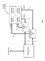
- FIG. 1 schematically illustrates an example of a touch responsive position sensor.
- the sensor includes a screen or panel 1 for sensing touch and associated circuitry for driving and sensing lines of the screen to detect a touch and position of the touch on the screen 1 .
- the overall touch screen 1 is formed of a 2 ⁇ 2 matrix of smaller touch screen areas 2 .
- the exemplary screen 1 includes four touch screen regions or areas 2 A to 2 D.
- the touch screen 1 has an array of sensing nodes formed at intersections of drive lines (horizontal X lines in the illustrated orientation) and sense lines (vertical Y lines in the illustrated orientation). A number of such nodes are included within each of the four touch screen regions or areas 2 A to 2 D.
- the X (drive) lines extend across all Y sense lines, for example, across both of the touch screen areas at the corresponding Y axis value.
- the Y lines extend across all of the X lines, for example, across both of the touch screen areas at the corresponding X axis value.
- each line would be connected from one screen to a corresponding line in the next adjacent screen in the appropriate X or Y direction. If the screens are logically separate, that is to say regions or areas of a continuous larger screen, then the lines could run continuously across the regions forming the overall screen, in the respective X and Y directions.
- the exemplary system for sensing touch and touch position on the screen 1 includes a number of control units. However, there are fewer control units than there are touch sensing areas 2 of the matrix of the touch screen 1 . In the 2 ⁇ 2 matrix example of FIG. 1 , there are two control units 3 A and 3 B.
- the system or device may also include a master control represented by the processor 4 in the example.
- a number of the X drive lines 5 connect to each of the control units 3 A and 3 B; and a number of the Y sense lines 6 connect to each of the control units 3 A and 3 B.
- Each control unit includes or may be a measuring device for measuring one or more parameters of signals at a number of nodes of the array of the touch screen 1 to determine a touch at or in the vicinity of the individual nodes the measurement device senses.
- the processor 4 serving as the master control connects to the control units 3 A, 3 B via data leads 7 .
- the processor 4 processes touch detection data from the control units to identify the node or nodes at which touch is detected on the overall area of screen 1 , based on timing of X line drive and sense line detection. Based on the node or nodes at which touch is detected, the processor 4 determines the position of each touch detected on the screen 1 .
- the processor 4 may also provide control signals to the control units 3 A and 3 B over the data leads 7 .
- the processor 4 also provides a higher level interface of the touch responsive position sensor to a system or device that uses the touch input information, for example, to a processor of a computer, personal digital assistant or mobile station.
- the example uses only two control units 3 A and 3 B. Screens having more areas, lines and/or sensing nodes at the line intersections would use a larger number of control units; and examples of such screens and the attendant configuration control units are discussed later.
- FIG. 1 implements drive line sharing.
- each set of the drive lines is driven by only one measurement device/control unit, but all of the drive lines are shared across multiple measurement devices for sensing purposes.
- Each individual X line is driven by only one control unit, but all of the measurement devices sense signals at some number the nodes on the particular X line. However, any one measurement device senses signals at nodes via only an appropriate number or subset of the sense lines connected to the measurement device.
- Each of the control units 3 A and 3 B drives and senses only the respective number of lines of each type within its design capacity. However, because the X drive lines extend across all Y sense lines, the X lines are shared by both of the control units 3 A and 3 B, in this first example. Each unit drives only the appropriate number of X lines. However, by synchronizing timing of the operations of the control units across the vertical sets of regions/lines (across the drive lines in the set of regions 2 A- 2 B and in the set of regions 2 C- 2 D), it becomes possible for each of the control units to sense touch at the Y lines that the respective unit connects to even when there is a touch at a crossing of an X line driven by the other control unit. In this way, the control units can work together to sample signals at the various nodes of a large screen 1 by the sharing of the X (drive) lines.
- control units 3 A and 3 B are synchronized.
- One or more of the drive (X) lines of each control unit may be used to synchronize the control units.
- the hardware of the control unit is configured to provide a separate synchronization component, freeing up all the drive (X) lines for actual use in touch sensing cycles.
- synchronization of the control units 3 A, 3 B may be provided by the processor 4 via data lines 7 .
- each measurement device or control unit 3 A or 3 B is configured to drive a first number of but not all of the X drive lines 5 extending across at least two of the sensing areas in the first direction.
- Each measurement device or control unit 3 A or 3 B also is configured to sense signals relating to a touch at nodes of intersection with all of the X drive lines 5 , via a second number of but not all of the sense lines 6 extending across at least two of the sensing areas 2 A- 2 C or 2 B- 2 D in the second direction.
- the measurement devices or control units 3 A and 3 B are configured to operate synchronously in a manner to identify one or more nodes, from among all nodes in all of the touch sensing areas 2 A- 2 D of the matrix of the touch screen 1 , as indication(s) of a position of a detected touch of the screen.
- FIG. 2 schematically illustrates an example of an apparatus for detecting a touch.
- the apparatus includes a control unit 10 provided with three switches 12 , 16 and 18 .
- Control unit 10 may be provided as a single integrated circuit chip such as a general purpose microprocessor, a microcontroller, a programmable logic device/array, an application-specific integrated circuit (ASIC), or a combination thereof.
- Switch 12 is provided between VDD and ground and is also connected to a sensor 13 .
- the self coupling capacitance of the sensor 13 is C X .
- the sensor 13 has two electrodes, an X (drive) electrode and a Y (sense) electrode.
- the apparatus measures the transverse coupling capacitance between the X and Y electrodes.
- the sensor 13 is connected in series to a sampling capacitor 15 having a sampling capacitance C S .
- the sampling capacitor 15 may have a sampling capacitance C S which is considerably larger than the sensor capacitance C X .
- the sampling capacitance C S is at least 1000 times larger than the sensor capacitance C X , where the sensor capacitance C X may be around 1 pF to 10 pF.
- the sampling capacitor 15 is also connected in series to the switches 16 and 18 , both of which are connected to ground.
- Capacitance C is a measure of the amount of electric charge stored for a given electric potential.
- V is the voltage between the plates and Q is charge.
- a voltage pulse is applied to the apparatus, by adjusting switch 12 to connect the sensor 13 to VDD, followed by closing switch 18 which causes charge to flow through C X into C S , accumulating charge at C S and C S .
- the sensor capacitance C X is then discharged, by, opening switch 18 , closing switch 16 and adjusting switch 12 to connect to ground. Since only the sensor capacitance C X is discharged after each voltage pulse, the capacitance C S held at the sampling capacitor 15 is increased with each voltage pulse. This step wise increase is illustrated in FIG. 3 , where V CS is the voltage accumulated at the sampling capacitor 15 .
- a predetermined number of voltage pulses is applied to the apparatus. After the predetermined number of pulses is applied to the apparatus, the capacitance C S accumulated in the sampling capacitor 15 is discharged. The time taken for the capacitance to discharge to a reference voltage is measured.
- the touch capacitance of the object diverts charge away from the drive electrode of C X to earth so that the capacitance C S accumulated in the sampling capacitor 15 with each voltage pulse is reduced.
- the sensor 13 is provided behind a dielectric panel so that the finger 19 does not directly contact the sensor 13 .
- the finger 19 may be provided in close proximity to the sensor 13 , but not directly contacting the sensor 13 .
- FIG. 5A illustrates the voltage V CS accumulated at the sampling capacitor 15 after the predetermined number of pulses when there is no touch, and the time required to discharge the sampling capacitor 15 .
- FIG. 5B illustrates the voltage V CS accumulated at the sampling capacitor 15 after the predetermined number of pulses when a user's finger 19 is close to or contacts the sensor 13 (i.e. when there is a touch), and the time required to discharge the sampling capacitor 15 . Since the sampling capacitor 15 is connected to the negative side of the sensor 13 , in the example of FIG. 2 , the accumulated voltage V CS has a negative value.
- the voltage V CS accumulated in FIG. 5B is reduced when compared to the voltage V CS accumulated in FIG. 5A .
- the time required to discharge the sampling capacitor 15 in FIG. 5B is reduced when compared to the time required to discharge the sampling capacitor 15 in FIG. 5A .
- the reduction in time required to discharge the sampling capacitor 15 in FIG. 5B indicates that there is a touch.
- the difference between the time required to discharge the sampling capacitor 15 when there is no touch (illustrated in FIG. 5A ) and the time required to discharge the sampling capacitor when there is a touch (illustrated in FIG. 5B ) is referred to as a delta.
- the detection of a delta indicates a touch, because the delta indicates that there has been a change of charge accumulated at the sampling capacitor 15 , when compared to the amount of charge expected to be accumulated at the sampling capacitor 15 when there is no touch.
- FIG. 6 illustrates a basic circuit for measuring the magnitude of Vcs.
- the control unit 10 of FIG. 2 includes a resistor 49 , switch 40 , a comparator 41 , a register 45 , a counter 43 and a clock signal 47 .
- the resistor 49 , comparator 41 and counter 43 are used to measure the magnitude of Vcs. The time required to discharge the sampling capacitor to a reference voltage is measured with the counter and the comparator, such that the counter value is the measurement.
- a plurality of drive and sense electrodes can be provided to create an array of sensing elements 220 (touch sensors 13 ) within a panel 210 of the position sensor.
- the drive electrodes (X) form one plate of each sensor 13 and the sense (Y) electrodes form the other plate of each sensor 13 having a capacitance C X .
- the position sensor also includes a plurality of resistors 230 , which may have different values, and a control unit 10 .
- FIG. 7 illustrates one exemplary matrix of eight sensing elements 220 , however many other configurations are possible.
- the basic measuring circuit illustrated in FIG. 6 and described above is provided as an example only. Other methods of measuring a touch can be used.
- the matrix of drive and sense electrodes forms a two-dimensional position sensor capable of sensing the position of a touch on the panel 210 .
- the control unit 10 uses a scanning sequence through the rows of drive electrodes and the columns of sense electrodes to measure coupling capacitance at the intersections or nodes.
- position sensors include touch screens and touch pads, which can be provided attached to or as part of computers, personal digital assistants (PDA), satellite navigation devices, mobile phones, portable media players, portable game consoles, public information kiosks, and point of sale systems etc. Position sensors can also be used as control panels on various appliances.
- FIG. 8 illustrates schematically four touch sensitive screens or regions, 50 A, 50 B, 50 C and 50 D, each having an array of sensing elements, arranged to create a large touch sensitive screen 500 .
- Each of the screens or regions 50 A to 50 D is connected to a respective control unit 520 A to 520 D.
- Each control unit 520 A to 520 D drives the X electrode lines 550 of its respective screen 50 A to 50 D and samples the Y electrode lines 540 of its respective screen 50 A to 50 D. Therefore, each control unit 520 A to 520 D forms a measuring device capable of detecting a touch and the position thereof on its respective screen 50 A to 50 D which makes up a part of (a quarter in FIG. 8 ) the overall screen 500 .
- Each control unit may be formed of a separate chip.
- each screen is logically or physically separated.
- the X lines and Y lines of FIG. 8 do not extend across the entire screen 500 .
- Each screen 50 A- 50 D has its own X lines and Y lines connected to its own control unit 520 A to 520 D.
- Each control unit 520 A to 520 D drives and senses signals at nodes within the area 50 A to 50 D that it controls.
- the X lines may extend only across the region controlled by the respective unit.
- the X drive lines 550 connected to the first control unit 520 A extend only across the first screen or area 50 A.
- the X drive lines 550 connected to the second control unit 520 B extend only across the second screen or area 50 B.
- the X drive lines 550 connected to the third control unit 520 C extend only across the third screen or area 50 C; and the X drive lines 550 connected to the fourth control unit 520 D extend only across the second screen or area 50 D.
- the sense lines extend only across the region controlled by the respective unit.
- Such an arrangement works much as if the areas 50 A to 50 D are actually separate screens.
- Each control unit 520 A to 520 D is only capable of driving and sensing a predetermined number of nodes, which limits the number of nodes in each respective screen or region 50 A to 50 D.
- each screen or area might have 10 X lines and 10 Y lines, and each control unit would be capable of driving/sensing 100 nodes.
- each screen might have 16 X lines and 14 Y lines, and each control unit would be capable of driving/sensing 224 nodes. Therefore in order to create and measure signals at nodes of a large touch screen 500 , such as illustrated in FIG.
- a large touch screen 500 for example nine times the size of a touch screen compatible with a single control unit chip of a particular capacity (e.g. a 3 ⁇ 3 touch screen), nine control units would be required. Furthermore, in order to create a large touch screen 500 , for example sixteen times the size of the basic touch screen unit (e.g. a 4 ⁇ 4 touch screen), sixteen control units would be required. Consequently, very large touch screens require very large numbers of control units.
- FIG. 9 illustrates an example of an alternative arrangement for creating a large touch sensitive screen by using shared X (drive) lines to enable drive/sensing of the larger number of nodes without necessarily requiring so many control units.
- the X (drive) lines are shared in that they extend across all Y sense lines of the screen connected to all of the control units 520 A to 520 C.
- the exemplary large touch screen 500 of FIG. 9 has nine individual touch screens or touch screen areas of the particular unit size in a 3 ⁇ 3 matrix arrangement.
- the control units have been combined, so that fewer control units are required.
- the control units of FIG. 9 work together to sample the large screen 500 by sharing the X (drive) lines.
- FIG. 10 illustrates the screen 500 of FIG. 9 in further detail.
- the large screen 500 is divided into nine touch screen areas 50 A to 50 I each of a size (e.g. number of nodes) corresponding to the capacity of one control unit.
- a separate control unit would measure signals from nodes in each screen area 50 A to 50 I.
- FIG. 9 enables each X line driven by one of the control units 520 A, 520 B, 520 C to be sampled by the Y lines of all of the control units 520 A, 520 B, 520 C.
- the control units 520 A, 520 B and 520 C are synchronized.
- at least one of the drive (X) lines of each control unit is used to synchronize the control units.
- five of the X lines are used for synchronization, resulting in each screen area 50 having 11 X lines and 14 Y lines.
- the hardware of the control unit is configured such that a separate synchronization component is provided, freeing up all the drive (X) lines for sensing.
- synchronization of the control units may be provided by a processor 530 , the processor 530 providing control signals 560 to each of the control units 520 A, 520 B, 520 C.
- FIG. 13 illustrates one method of detecting a touch using the arrangement of FIG. 9 .
- the process is initiated at step 300 .
- sampling is initiated.
- each X line is sampled using the Y lines associated with all the control units in the system.
- one control unit drives the X lines in the set connected to that unit.
- the control units that are not driving the X lines connected to those units at any given point in time provide a dummy sample, so that the X lines of the one control unit can be sampled by all the Y lines of all of the control units in the system.
- Data signals 560 from each control unit 520 A, 520 B and 520 C are transferred to a processor 530 at step 330 .
- the processor 530 is provided for sensing a touch or a proximity of an object and determining its position on the overall screen based on the received sense signals.
- the processor 530 processes all the data received from all of the control units 520 A, 520 B and 520 C and determines if there has/has not been a touch at the touch screen 500 .
- a processor 530 is used to process the data since each control unit 520 A, 520 B and 520 C is not aware of the data produced by the other control units 520 A, 520 B and 520 C.
- the processor 530 receives data from all the control unit 520 A, 520 B and 520 C so is able to eliminate nonlinearities at the screen area 50 A to 50 I boundaries.
- the processor 530 may be any known processor, such as a microcontroller, microprocessor or central processor.
- the processor 530 is connected to an interface 570 , which connects to the device in which the touch screen is provided.
- each control unit 520 A, 520 B, 520 C may be provided with its own processor. In such an example, it is possible for all the data to be transferred to one of the control units 520 A, 520 B or 520 C for processing at that control unit 520 A, 520 B or 520 C. The data from all of the control units 520 A, 520 B, 520 C is processed together at one of the control unit 520 A, 520 B or 520 C to eliminate nonlinearities at the screen area 50 A to 50 I boundaries.
- FIG. 14 illustrates another method of detecting a touch using the arrangement of FIG. 9 .
- the process is initiated at step 400 .
- sampling is initiated.
- each X line is sampled using the Y lines associated with all the control units in the system. The control units that are not driving the X lines at any given point in time provide a dummy sample, so the X lines of one control unit can be sampled by all the Y lines of all of the control units in the system.
- Data signals 560 from each control unit in the system are transferred to a processor 530 at step 420 .
- the processor 530 processes all the data received from all of the control units 520 A, 520 B and 520 C and determines if there has/has not been at touch at the touch screen 500 .
- the process of FIG. 14 can be utilized, for example, when a separate synchronization component is provided, or when the processor 530 controls synchronization of the control units 520 A, 520 B, 520 C.
- the process of FIG. 14 can also be utilized, for example, when each control unit 520 A, 520 B, 520 C is provided with its own processor. In such an example, all the data would be transferred to one of the control units 520 A, 520 B or 520 C for processing at that control unit 520 A, 520 B or 520 C.
- FIGS. 9 and 10 were described with reference to a large touch screen 500 , having a 3 ⁇ 3 arrangements, the present subject matter may also be utilized to create a large touch screen 500 having a 2 ⁇ 2 arrangement like that of FIG. 1 , requiring two control units; a 4 ⁇ 4 arrangement, requiring four control units; a 5 ⁇ 5 arrangement, requiring five control units etc.
- the drive line sharing technologies may also be utilized to create a large touch screen 500 having a 2 ⁇ 4 arrangement, 3 ⁇ 4 arrangement etc. as required. In such an arrangement, the touch screen would require four control units.
- the control units that are not driving the X lines, or Y lines as appropriate may provide a dummy sample instead.
- FIG. 11 illustrates schematically a panel 210 including a plurality of drive (X) electrode lines (not illustrated) connected to drive channels 280 and a plurality of sense (Y) electrode lines (not illustrated) connected to sense channels 240 .
- the drive channels 280 and the sense channels 240 are connected to a control unit 200 via a connector 270 .
- the connector 270 may be a conductive trace or a feed-through.
- the control unit 200 includes a drive unit 120 for supplying drive signals to the drive electrodes, and a sense unit 140 for sensing signals from the sense electrodes.
- the control unit 200 thus controls the operation of the drive and sense units 120 , 140 .
- the control unit 200 may also include a storage device 180 , such as a computer readable medium.
- drive unit 120 and sensing unit 140 are illustrated as separate components in FIG. 11 , the functionality of these units may be provided in a single integrated circuit chip such as a general purpose microprocessor, a microcontroller, a field programmable gate array (FPGA) or an application specific integrated circuit (ASIC).
- a separate drive unit may be provided for each drive channel connected to each electrode.
- the drive channels Xn, Xn+1, Xn+2, . . . Xn+m are connected to the drive unit 120 , although in one example, each drive channel is connected to a separate drive unit 120 .
- the sense channels Yn, Yn+1, Yn+2, . . . Yn+m are connected to the sense unit 140 .
- a drive control units may include a drive unit and a storage device
- a sense control units may include a sense unit and a storage device. If a large touch screen 500 having a 2 ⁇ 4 arrangement etc. is provided, then it may be advantageous to use two drive control units and four sense control units etc.
- the above examples show that the drive line sharing approach provides an efficient technique to scale the electronics to measure more nodes on larger touch panels.
- the first example used two control units to perform drive and sensing on a 2 ⁇ 2 matrix touch panel.
- the second example used three control units to perform drive and sensing on a 3 ⁇ 3 matrix touch panel.
- a similar approach can be used for larger and larger square matrix panels, with one additional control unit/measuring device for each additional row/column.
- the shared drive line strategy to scaling the number of control units also may be adapted to panel configurations that utilize different numbers of screens or areas in the different panel dimensions. For example, each control unit might handle less than its full capacity of drive or sense lines but handle its full capacity of the other type of lines. Alternatively, one controller might only drive a set of X lines for a row of regions or only sense a set of Y lines for a column of regions.
- the position sensors described above can be attached to numerous electronic devices, such as computers, personal digital assistants (PDA), satellite navigation devices, mobile phones, portable media players, portable game consoles, public information kiosks, point of sale systems etc.
- electronic devices may include a central processor or other processing device for executing program instructions, an internal communication bus, various types of memory or storage media (RAM, ROM, EEPROM, cache memory, disk drives etc.) for code and data storage, and one or more network interface cards or ports for communication purposes.
Landscapes
- Engineering & Computer Science (AREA)
- General Engineering & Computer Science (AREA)
- Theoretical Computer Science (AREA)
- Human Computer Interaction (AREA)
- Physics & Mathematics (AREA)
- General Physics & Mathematics (AREA)
- Computer Networks & Wireless Communication (AREA)
- Position Input By Displaying (AREA)
- User Interface Of Digital Computer (AREA)
Abstract
Description
Claims (21)
Priority Applications (6)
| Application Number | Priority Date | Filing Date | Title |
|---|---|---|---|
| US12/771,583 US8860686B2 (en) | 2010-04-30 | 2010-04-30 | Multi-chip touch screens |
| TW100111110A TWI518563B (en) | 2010-04-30 | 2011-03-30 | Multi-chip touch screens |
| DE102011007169A DE102011007169A1 (en) | 2010-04-30 | 2011-04-12 | Multichip touch screen |
| CN201110103397.3A CN102236466B (en) | 2010-04-30 | 2011-04-20 | Multi-chip touch screens |
| JP2011114135A JP2011238240A (en) | 2010-04-30 | 2011-04-28 | Multi-chip touch screen |
| KR1020110041201A KR101687035B1 (en) | 2010-04-30 | 2011-04-29 | Multi-chip touch screens |
Applications Claiming Priority (1)
| Application Number | Priority Date | Filing Date | Title |
|---|---|---|---|
| US12/771,583 US8860686B2 (en) | 2010-04-30 | 2010-04-30 | Multi-chip touch screens |
Publications (2)
| Publication Number | Publication Date |
|---|---|
| US20110267304A1 US20110267304A1 (en) | 2011-11-03 |
| US8860686B2 true US8860686B2 (en) | 2014-10-14 |
Family
ID=44786620
Family Applications (1)
| Application Number | Title | Priority Date | Filing Date |
|---|---|---|---|
| US12/771,583 Active 2031-04-09 US8860686B2 (en) | 2010-04-30 | 2010-04-30 | Multi-chip touch screens |
Country Status (6)
| Country | Link |
|---|---|
| US (1) | US8860686B2 (en) |
| JP (1) | JP2011238240A (en) |
| KR (1) | KR101687035B1 (en) |
| CN (1) | CN102236466B (en) |
| DE (1) | DE102011007169A1 (en) |
| TW (1) | TWI518563B (en) |
Cited By (5)
| Publication number | Priority date | Publication date | Assignee | Title |
|---|---|---|---|---|
| US9628594B2 (en) * | 2014-10-31 | 2017-04-18 | Semtech Corporation | Method and device for capacitive near-field communication in mobile devices |
| US9916055B2 (en) | 2015-04-17 | 2018-03-13 | Silicon Works Co., Ltd. | Multi-chip touch system and control method therefor |
| US20190078954A1 (en) * | 2017-09-14 | 2019-03-14 | Huf Hülsbeck & Fürst Gmbh & Co. Kg | Arrangement |
| US10558288B2 (en) | 2016-07-07 | 2020-02-11 | Samsung Display Co., Ltd. | Multi-touch display panel and method of controlling the same |
| US11675455B2 (en) | 2020-10-29 | 2023-06-13 | Samsung Display Co., Ltd. | Electronic device including a sensor layer |
Families Citing this family (42)
| Publication number | Priority date | Publication date | Assignee | Title |
|---|---|---|---|---|
| TWI434207B (en) * | 2010-03-25 | 2014-04-11 | Novatek Microelectronics Corp | Touch sensing system, electronic touch apparatus, and touch sensing method |
| TWM400618U (en) * | 2010-08-13 | 2011-03-21 | Mastouch Optoelectronics Technologies Co Ltd | Projected capacitive touch panel |
| US20130015906A1 (en) * | 2011-07-13 | 2013-01-17 | Silicon Integrated Systems Corp. | Touch Panel Device |
| US20130016051A1 (en) * | 2011-07-13 | 2013-01-17 | Silicon Integrated Systems Corp. | Touch Panel Device Having a Divided ITO layer for Reducing Loading |
| TWI451304B (en) * | 2011-11-04 | 2014-09-01 | Innolux Corp | Touch apparatus and driving method therof |
| CN103092383B (en) * | 2011-11-04 | 2016-06-15 | 群康科技(深圳)有限公司 | Contactor control device and driving method thereof |
| CN103455195A (en) * | 2012-04-18 | 2013-12-18 | 矽统科技股份有限公司 | Touch screen device |
| KR101374018B1 (en) * | 2012-04-24 | 2014-03-12 | 엘지디스플레이 주식회사 | Apparatus and method for driving touch screen |
| CN102855019A (en) * | 2012-09-03 | 2013-01-02 | 福建华映显示科技有限公司 | Multi-touch screen device and operating method thereof |
| KR102019776B1 (en) * | 2012-10-15 | 2019-09-11 | 삼성디스플레이 주식회사 | Touch sensing system |
| KR102016572B1 (en) * | 2012-11-28 | 2019-09-02 | 엘지디스플레이 주식회사 | Touch sensing system |
| TWI549025B (en) * | 2013-05-08 | 2016-09-11 | 廣達電腦股份有限公司 | Touch panel |
| US20160103500A1 (en) * | 2013-05-21 | 2016-04-14 | Stanley Innovation, Inc. | System and method for a human machine interface utilizing near-field quasi-state electrical field sensing technology |
| KR102088906B1 (en) * | 2013-06-28 | 2020-03-13 | 엘지디스플레이 주식회사 | Appratus and method for driving touch screen |
| KR102108287B1 (en) | 2013-08-30 | 2020-05-28 | 주식회사 실리콘웍스 | Touch system and control method thereof |
| KR102120776B1 (en) | 2013-09-16 | 2020-06-11 | 주식회사 리딩유아이 | Touch panel |
| CN103530012A (en) * | 2013-10-31 | 2014-01-22 | 中环高科(天津)股份有限公司 | Method for adopting single touch drive module to drive multiple capacitive touch screens |
| KR102138594B1 (en) * | 2013-12-20 | 2020-07-28 | 엘지디스플레이 주식회사 | Touch screen display |
| US9372584B2 (en) * | 2014-01-09 | 2016-06-21 | Synaptics Incorporated | Mitigating electrode interference in an integrated input device |
| CN104133594B (en) * | 2014-08-12 | 2017-03-22 | 友达光电(苏州)有限公司 | Touch panel and detecting method suitable for touch panel |
| KR101677334B1 (en) | 2014-10-24 | 2016-11-17 | 엘지전자 주식회사 | Refrigerator door |
| CN105588400B (en) * | 2014-11-07 | 2018-04-13 | Lg电子株式会社 | Refrigerator and controlling method for refrigerator |
| WO2016072802A1 (en) | 2014-11-07 | 2016-05-12 | Lg Electronics Inc. | Metal touch sensing apparatus, and home appliance having metal touch sensing apparatus and method for controlling the same |
| KR101659180B1 (en) | 2014-12-22 | 2016-09-22 | 엘지전자 주식회사 | Tuch sensor assembly and refrigerator door with Tuch sensor assembly |
| KR101659181B1 (en) | 2014-12-22 | 2016-09-30 | 엘지전자 주식회사 | Tuch sensor assembly and refrigerator door with Tuch sensor assembly |
| KR101668922B1 (en) | 2014-12-24 | 2016-10-24 | 엘지전자 주식회사 | Home appliance display assembly and manufacture method thereof |
| KR101668921B1 (en) | 2014-12-24 | 2016-10-24 | 엘지전자 주식회사 | Tuch sensor assembly and refrigerator door with Tuch sensor assembly |
| KR101659184B1 (en) | 2014-12-24 | 2016-09-22 | 엘지전자 주식회사 | Tuch sensor assembly and manufacture method of tuch sensor assembly |
| CN105988628A (en) * | 2015-02-26 | 2016-10-05 | 宏碁股份有限公司 | Touch device and control method |
| CN104820522B (en) * | 2015-05-14 | 2018-04-06 | 南昌欧菲光科技有限公司 | Utilize the multi-screen synchronous contactor control device and method from appearance characteristic |
| CN108351718B (en) * | 2015-10-19 | 2021-04-23 | 富士胶片株式会社 | Indication receiving device, information processing device, signal processing method and storage medium |
| US20190004625A1 (en) * | 2015-10-29 | 2019-01-03 | Hewlett-Packard Development Company ,L.P. | Touch device |
| KR101736608B1 (en) | 2015-11-27 | 2017-05-16 | 엘지전자 주식회사 | Refrigerator |
| CN108614643A (en) * | 2016-09-23 | 2018-10-02 | 李璇 | The large-scale touch-screen system of multi-chip |
| US10503312B2 (en) * | 2018-01-18 | 2019-12-10 | Elo Touch Solutions, Inc. | Large PCAP screen with multiple touch controller ASICS with interleaved receiver connections |
| DE112019002844T5 (en) | 2018-06-06 | 2021-02-25 | Wacom Co., Ltd. | PIN DETECTION SYSTEM |
| CN109471557B (en) * | 2018-10-31 | 2021-10-26 | 合肥鑫晟光电科技有限公司 | Control circuit and control method of tiled display screen and tiled display device |
| CN109752618A (en) * | 2019-03-22 | 2019-05-14 | 敦泰电子有限公司 | A kind of combination of touch screen detection chip and terminal device |
| CN113535001B (en) * | 2021-07-24 | 2024-01-23 | 中航华东光电有限公司 | Cascade driving technical method for large-size capacitive touch screen |
| CN113970987B (en) * | 2021-10-18 | 2025-01-21 | 中航华东光电有限公司 | Multi-chip cascade capacitive touch screen driving system and method |
| EP4458191A4 (en) * | 2021-12-28 | 2025-11-26 | Japan Tobacco Inc | Aerosol generation device, process and program |
| WO2023127109A1 (en) * | 2021-12-28 | 2023-07-06 | 日本たばこ産業株式会社 | Aerosol generation device, method, and program |
Citations (19)
| Publication number | Priority date | Publication date | Assignee | Title |
|---|---|---|---|---|
| US20040135775A1 (en) * | 1999-12-06 | 2004-07-15 | Hurst G Samuel | Touch screen with relatively conductive grid |
| US20070200833A1 (en) * | 2006-02-24 | 2007-08-30 | Samsung Electronics Co., Ltd. | Display device and method of controlling touch detection unit |
| US20090250268A1 (en) * | 2008-02-08 | 2009-10-08 | Staton Kenneth L | Method for rapidly testing capacitance sensing array fault conditions |
| US20090267903A1 (en) * | 2008-04-23 | 2009-10-29 | Motorola, Inc. | Multi-Touch Detection Panel with Disambiguation of Touch Coordinates |
| US20090315854A1 (en) | 2008-06-18 | 2009-12-24 | Epson Imaging Devices Corporation | Capacitance type input device and display device with input function |
| US7663607B2 (en) | 2004-05-06 | 2010-02-16 | Apple Inc. | Multipoint touchscreen |
| US20100156811A1 (en) * | 2008-12-22 | 2010-06-24 | Ding Hua Long | New pattern design for a capacitive touch screen |
| US7875814B2 (en) | 2005-07-21 | 2011-01-25 | Tpo Displays Corp. | Electromagnetic digitizer sensor array structure |
| US7920129B2 (en) | 2007-01-03 | 2011-04-05 | Apple Inc. | Double-sided touch-sensitive panel with shield and drive combined layer |
| US8031094B2 (en) | 2009-09-11 | 2011-10-04 | Apple Inc. | Touch controller with improved analog front end |
| US8031174B2 (en) | 2007-01-03 | 2011-10-04 | Apple Inc. | Multi-touch surface stackup arrangement |
| US8040326B2 (en) | 2007-06-13 | 2011-10-18 | Apple Inc. | Integrated in-plane switching display and touch sensor |
| US8049732B2 (en) | 2007-01-03 | 2011-11-01 | Apple Inc. | Front-end signal compensation |
| US8179381B2 (en) | 2008-02-28 | 2012-05-15 | 3M Innovative Properties Company | Touch screen sensor |
| WO2012129247A2 (en) | 2011-03-21 | 2012-09-27 | Apple Inc. | Electronic devices with flexible displays |
| US20120242588A1 (en) | 2011-03-21 | 2012-09-27 | Myers Scott A | Electronic devices with concave displays |
| US20120243151A1 (en) | 2011-03-21 | 2012-09-27 | Stephen Brian Lynch | Electronic Devices With Convex Displays |
| US20120243719A1 (en) | 2011-03-21 | 2012-09-27 | Franklin Jeremy C | Display-Based Speaker Structures for Electronic Devices |
| US20120242592A1 (en) | 2011-03-21 | 2012-09-27 | Rothkopf Fletcher R | Electronic devices with flexible displays |
Family Cites Families (13)
| Publication number | Priority date | Publication date | Assignee | Title |
|---|---|---|---|---|
| JPH06250786A (en) * | 1993-02-23 | 1994-09-09 | Matsushita Electric Ind Co Ltd | Matrix type display panel and coordinate input device using the same |
| JP3170415B2 (en) * | 1994-05-23 | 2001-05-28 | シャープ株式会社 | Electrostatic coupling input device |
| JPH09167047A (en) * | 1995-12-14 | 1997-06-24 | Fujitsu Takamizawa Component Kk | Coordinate detector and error correcting method |
| KR20000039893A (en) * | 1998-12-16 | 2000-07-05 | 구자홍 | Touch panel circuit |
| JP4159848B2 (en) * | 2002-10-11 | 2008-10-01 | シチズンホールディングス株式会社 | Liquid crystal device and manufacturing method thereof |
| EP2075678A3 (en) * | 2007-12-27 | 2013-03-13 | TPO Displays Corp. | Position sensing display |
| JP2009180846A (en) * | 2008-01-30 | 2009-08-13 | Toshiba Corp | Information processing device |
| US20090231288A1 (en) * | 2008-03-17 | 2009-09-17 | Inventec Corporation | Hand-held electronic device and combined input method thereof |
| TW200943155A (en) * | 2008-04-02 | 2009-10-16 | Elan Microelectronics Corp | Capacitor-type touch device and data transmission method applied to the capacitor-type touch device |
| JP2010039510A (en) * | 2008-07-31 | 2010-02-18 | Pentel Corp | Method of producing electrostatic capacity coupling type coordinate input panel |
| JP5229887B2 (en) * | 2008-08-06 | 2013-07-03 | 株式会社ワコム | Position detection device |
| US8866840B2 (en) * | 2008-09-08 | 2014-10-21 | Qualcomm Incorporated | Sending a parameter based on screen size or screen resolution of a multi-panel electronic device to a server |
| JP5216495B2 (en) * | 2008-09-16 | 2013-06-19 | 株式会社ジャパンディスプレイウェスト | Contact detection device and display device |
-
2010
- 2010-04-30 US US12/771,583 patent/US8860686B2/en active Active
-
2011
- 2011-03-30 TW TW100111110A patent/TWI518563B/en active
- 2011-04-12 DE DE102011007169A patent/DE102011007169A1/en active Pending
- 2011-04-20 CN CN201110103397.3A patent/CN102236466B/en active Active
- 2011-04-28 JP JP2011114135A patent/JP2011238240A/en active Pending
- 2011-04-29 KR KR1020110041201A patent/KR101687035B1/en active Active
Patent Citations (19)
| Publication number | Priority date | Publication date | Assignee | Title |
|---|---|---|---|---|
| US20040135775A1 (en) * | 1999-12-06 | 2004-07-15 | Hurst G Samuel | Touch screen with relatively conductive grid |
| US7663607B2 (en) | 2004-05-06 | 2010-02-16 | Apple Inc. | Multipoint touchscreen |
| US7875814B2 (en) | 2005-07-21 | 2011-01-25 | Tpo Displays Corp. | Electromagnetic digitizer sensor array structure |
| US20070200833A1 (en) * | 2006-02-24 | 2007-08-30 | Samsung Electronics Co., Ltd. | Display device and method of controlling touch detection unit |
| US8049732B2 (en) | 2007-01-03 | 2011-11-01 | Apple Inc. | Front-end signal compensation |
| US7920129B2 (en) | 2007-01-03 | 2011-04-05 | Apple Inc. | Double-sided touch-sensitive panel with shield and drive combined layer |
| US8031174B2 (en) | 2007-01-03 | 2011-10-04 | Apple Inc. | Multi-touch surface stackup arrangement |
| US8040326B2 (en) | 2007-06-13 | 2011-10-18 | Apple Inc. | Integrated in-plane switching display and touch sensor |
| US20090250268A1 (en) * | 2008-02-08 | 2009-10-08 | Staton Kenneth L | Method for rapidly testing capacitance sensing array fault conditions |
| US8179381B2 (en) | 2008-02-28 | 2012-05-15 | 3M Innovative Properties Company | Touch screen sensor |
| US20090267903A1 (en) * | 2008-04-23 | 2009-10-29 | Motorola, Inc. | Multi-Touch Detection Panel with Disambiguation of Touch Coordinates |
| US20090315854A1 (en) | 2008-06-18 | 2009-12-24 | Epson Imaging Devices Corporation | Capacitance type input device and display device with input function |
| US20100156811A1 (en) * | 2008-12-22 | 2010-06-24 | Ding Hua Long | New pattern design for a capacitive touch screen |
| US8031094B2 (en) | 2009-09-11 | 2011-10-04 | Apple Inc. | Touch controller with improved analog front end |
| WO2012129247A2 (en) | 2011-03-21 | 2012-09-27 | Apple Inc. | Electronic devices with flexible displays |
| US20120242588A1 (en) | 2011-03-21 | 2012-09-27 | Myers Scott A | Electronic devices with concave displays |
| US20120243151A1 (en) | 2011-03-21 | 2012-09-27 | Stephen Brian Lynch | Electronic Devices With Convex Displays |
| US20120243719A1 (en) | 2011-03-21 | 2012-09-27 | Franklin Jeremy C | Display-Based Speaker Structures for Electronic Devices |
| US20120242592A1 (en) | 2011-03-21 | 2012-09-27 | Rothkopf Fletcher R | Electronic devices with flexible displays |
Non-Patent Citations (4)
| Title |
|---|
| Hung, J-W, "TANGO Capacitive Touch Controller IC", PIXCIR AG, Switzerland © 2008. |
| U.S. Appl. No. 61/454,894, filed Mar. 21, 2011, Rothkopf. |
| U.S. Appl. No. 61/454,936, filed Mar. 21, 2011, Myers. |
| U.S. Appl. No. 61/454,950, filed Mar. 21, 2011, Lynch. |
Cited By (7)
| Publication number | Priority date | Publication date | Assignee | Title |
|---|---|---|---|---|
| US9628594B2 (en) * | 2014-10-31 | 2017-04-18 | Semtech Corporation | Method and device for capacitive near-field communication in mobile devices |
| US10396855B2 (en) | 2014-10-31 | 2019-08-27 | Semtech Corporation | Method and device for capacitive near-field communication in mobile devices |
| US9916055B2 (en) | 2015-04-17 | 2018-03-13 | Silicon Works Co., Ltd. | Multi-chip touch system and control method therefor |
| US10558288B2 (en) | 2016-07-07 | 2020-02-11 | Samsung Display Co., Ltd. | Multi-touch display panel and method of controlling the same |
| US20190078954A1 (en) * | 2017-09-14 | 2019-03-14 | Huf Hülsbeck & Fürst Gmbh & Co. Kg | Arrangement |
| US10837850B2 (en) * | 2017-09-14 | 2020-11-17 | Huf Hülsbeck & Fürst Gmbh & Co. Kg | Arrangement for an evaluation in a capacitive sensor device of a vehicle |
| US11675455B2 (en) | 2020-10-29 | 2023-06-13 | Samsung Display Co., Ltd. | Electronic device including a sensor layer |
Also Published As
| Publication number | Publication date |
|---|---|
| DE102011007169A1 (en) | 2011-11-03 |
| CN102236466A (en) | 2011-11-09 |
| TWI518563B (en) | 2016-01-21 |
| TW201205381A (en) | 2012-02-01 |
| KR101687035B1 (en) | 2016-12-15 |
| CN102236466B (en) | 2016-01-20 |
| KR20110121590A (en) | 2011-11-07 |
| US20110267304A1 (en) | 2011-11-03 |
| JP2011238240A (en) | 2011-11-24 |
Similar Documents
| Publication | Publication Date | Title |
|---|---|---|
| US8860686B2 (en) | Multi-chip touch screens | |
| US10754457B2 (en) | Touch-screen panel with multiple sense units and related methods | |
| US12124657B2 (en) | Passive touch detection for capacitive sense array | |
| US8766929B2 (en) | Panel for position sensors | |
| US11481066B2 (en) | Providing a baseline capacitance for a capacitance sensing channel | |
| US8937611B2 (en) | Capacitive touch sensors | |
| EP2184666B1 (en) | Multipoint sensing method applicable to capacitive touch panel | |
| US9013441B2 (en) | Smart scanning for a capacitive sensing array | |
| US10228780B2 (en) | Stylus to host synchronization using a magnetic field | |
| US10572068B2 (en) | Uniformity correction method for low cost and non-rectangular touch sensor matrices | |
| US20120182252A1 (en) | Differential Capacitive Touchscreen or Touch Panel | |
| US10613695B2 (en) | Integrated touch sensing and force sensing in a touch detection device | |
| TW201248475A (en) | Capacitance sensing devices and control methods | |
| US10528178B2 (en) | Capacitive touch sensing with conductivity type determination | |
| TWI536231B (en) | Multi-touch detection method and device thereof | |
| KR101671835B1 (en) | Apparatus and method for non-touch testing touch screen module |
Legal Events
| Date | Code | Title | Description |
|---|---|---|---|
| AS | Assignment |
Owner name: ATMEL CORPORATION, CALIFORNIA Free format text: ASSIGNMENT OF ASSIGNORS INTEREST;ASSIGNOR:QRG LIMITED;REEL/FRAME:024608/0123 Effective date: 20100625 Owner name: QRG LIMITED, UNITED KINGDOM Free format text: ASSIGNMENT OF ASSIGNORS INTEREST;ASSIGNORS:SIMMONS, MARTIN JOHN;PICKETT, DAN THOMAS EDWARD;COLLINS, RICHARD PAUL;REEL/FRAME:024608/0094 Effective date: 20100618 |
|
| AS | Assignment |
Owner name: MORGAN STANLEY SENIOR FUNDING, INC. AS ADMINISTRATIVE AGENT, NEW YORK Free format text: PATENT SECURITY AGREEMENT;ASSIGNOR:ATMEL CORPORATION;REEL/FRAME:031912/0173 Effective date: 20131206 Owner name: MORGAN STANLEY SENIOR FUNDING, INC. AS ADMINISTRAT Free format text: PATENT SECURITY AGREEMENT;ASSIGNOR:ATMEL CORPORATION;REEL/FRAME:031912/0173 Effective date: 20131206 |
|
| STCF | Information on status: patent grant |
Free format text: PATENTED CASE |
|
| AS | Assignment |
Owner name: ATMEL CORPORATION, CALIFORNIA Free format text: TERMINATION AND RELEASE OF SECURITY INTEREST IN PATENT COLLATERAL;ASSIGNOR:MORGAN STANLEY SENIOR FUNDING, INC.;REEL/FRAME:038376/0001 Effective date: 20160404 |
|
| AS | Assignment |
Owner name: JPMORGAN CHASE BANK, N.A., AS ADMINISTRATIVE AGENT, ILLINOIS Free format text: SECURITY INTEREST;ASSIGNOR:ATMEL CORPORATION;REEL/FRAME:041715/0747 Effective date: 20170208 Owner name: JPMORGAN CHASE BANK, N.A., AS ADMINISTRATIVE AGENT Free format text: SECURITY INTEREST;ASSIGNOR:ATMEL CORPORATION;REEL/FRAME:041715/0747 Effective date: 20170208 |
|
| MAFP | Maintenance fee payment |
Free format text: PAYMENT OF MAINTENANCE FEE, 4TH YEAR, LARGE ENTITY (ORIGINAL EVENT CODE: M1551) Year of fee payment: 4 |
|
| AS | Assignment |
Owner name: JPMORGAN CHASE BANK, N.A., AS ADMINISTRATIVE AGENT, ILLINOIS Free format text: SECURITY INTEREST;ASSIGNORS:MICROCHIP TECHNOLOGY INCORPORATED;SILICON STORAGE TECHNOLOGY, INC.;ATMEL CORPORATION;AND OTHERS;REEL/FRAME:046426/0001 Effective date: 20180529 Owner name: JPMORGAN CHASE BANK, N.A., AS ADMINISTRATIVE AGENT Free format text: SECURITY INTEREST;ASSIGNORS:MICROCHIP TECHNOLOGY INCORPORATED;SILICON STORAGE TECHNOLOGY, INC.;ATMEL CORPORATION;AND OTHERS;REEL/FRAME:046426/0001 Effective date: 20180529 |
|
| AS | Assignment |
Owner name: WELLS FARGO BANK, NATIONAL ASSOCIATION, AS NOTES COLLATERAL AGENT, CALIFORNIA Free format text: SECURITY INTEREST;ASSIGNORS:MICROCHIP TECHNOLOGY INCORPORATED;SILICON STORAGE TECHNOLOGY, INC.;ATMEL CORPORATION;AND OTHERS;REEL/FRAME:047103/0206 Effective date: 20180914 Owner name: WELLS FARGO BANK, NATIONAL ASSOCIATION, AS NOTES C Free format text: SECURITY INTEREST;ASSIGNORS:MICROCHIP TECHNOLOGY INCORPORATED;SILICON STORAGE TECHNOLOGY, INC.;ATMEL CORPORATION;AND OTHERS;REEL/FRAME:047103/0206 Effective date: 20180914 |
|
| AS | Assignment |
Owner name: JPMORGAN CHASE BANK, N.A., AS ADMINISTRATIVE AGENT, DELAWARE Free format text: SECURITY INTEREST;ASSIGNORS:MICROCHIP TECHNOLOGY INC.;SILICON STORAGE TECHNOLOGY, INC.;ATMEL CORPORATION;AND OTHERS;REEL/FRAME:053311/0305 Effective date: 20200327 |
|
| AS | Assignment |
Owner name: SILICON STORAGE TECHNOLOGY, INC., ARIZONA Free format text: RELEASE BY SECURED PARTY;ASSIGNOR:JPMORGAN CHASE BANK, N.A, AS ADMINISTRATIVE AGENT;REEL/FRAME:053466/0011 Effective date: 20200529 Owner name: MICROCHIP TECHNOLOGY INC., ARIZONA Free format text: RELEASE BY SECURED PARTY;ASSIGNOR:JPMORGAN CHASE BANK, N.A, AS ADMINISTRATIVE AGENT;REEL/FRAME:053466/0011 Effective date: 20200529 Owner name: MICROSEMI STORAGE SOLUTIONS, INC., ARIZONA Free format text: RELEASE BY SECURED PARTY;ASSIGNOR:JPMORGAN CHASE BANK, N.A, AS ADMINISTRATIVE AGENT;REEL/FRAME:053466/0011 Effective date: 20200529 Owner name: MICROSEMI CORPORATION, CALIFORNIA Free format text: RELEASE BY SECURED PARTY;ASSIGNOR:JPMORGAN CHASE BANK, N.A, AS ADMINISTRATIVE AGENT;REEL/FRAME:053466/0011 Effective date: 20200529 Owner name: ATMEL CORPORATION, ARIZONA Free format text: RELEASE BY SECURED PARTY;ASSIGNOR:JPMORGAN CHASE BANK, N.A, AS ADMINISTRATIVE AGENT;REEL/FRAME:053466/0011 Effective date: 20200529 |
|
| AS | Assignment |
Owner name: WELLS FARGO BANK, NATIONAL ASSOCIATION, MINNESOTA Free format text: SECURITY INTEREST;ASSIGNORS:MICROCHIP TECHNOLOGY INC.;SILICON STORAGE TECHNOLOGY, INC.;ATMEL CORPORATION;AND OTHERS;REEL/FRAME:053468/0705 Effective date: 20200529 |
|
| AS | Assignment |
Owner name: WELLS FARGO BANK, NATIONAL ASSOCIATION, AS COLLATERAL AGENT, MINNESOTA Free format text: SECURITY INTEREST;ASSIGNORS:MICROCHIP TECHNOLOGY INCORPORATED;SILICON STORAGE TECHNOLOGY, INC.;ATMEL CORPORATION;AND OTHERS;REEL/FRAME:055671/0612 Effective date: 20201217 |
|
| AS | Assignment |
Owner name: WELLS FARGO BANK, NATIONAL ASSOCIATION, AS NOTES COLLATERAL AGENT, MINNESOTA Free format text: SECURITY INTEREST;ASSIGNORS:MICROCHIP TECHNOLOGY INCORPORATED;SILICON STORAGE TECHNOLOGY, INC.;ATMEL CORPORATION;AND OTHERS;REEL/FRAME:057935/0474 Effective date: 20210528 |
|
| AS | Assignment |
Owner name: MICROSEMI STORAGE SOLUTIONS, INC., ARIZONA Free format text: RELEASE BY SECURED PARTY;ASSIGNOR:JPMORGAN CHASE BANK, N.A., AS ADMINISTRATIVE AGENT;REEL/FRAME:059333/0222 Effective date: 20220218 Owner name: MICROSEMI CORPORATION, ARIZONA Free format text: RELEASE BY SECURED PARTY;ASSIGNOR:JPMORGAN CHASE BANK, N.A., AS ADMINISTRATIVE AGENT;REEL/FRAME:059333/0222 Effective date: 20220218 Owner name: ATMEL CORPORATION, ARIZONA Free format text: RELEASE BY SECURED PARTY;ASSIGNOR:JPMORGAN CHASE BANK, N.A., AS ADMINISTRATIVE AGENT;REEL/FRAME:059333/0222 Effective date: 20220218 Owner name: SILICON STORAGE TECHNOLOGY, INC., ARIZONA Free format text: RELEASE BY SECURED PARTY;ASSIGNOR:JPMORGAN CHASE BANK, N.A., AS ADMINISTRATIVE AGENT;REEL/FRAME:059333/0222 Effective date: 20220218 Owner name: MICROCHIP TECHNOLOGY INCORPORATED, ARIZONA Free format text: RELEASE BY SECURED PARTY;ASSIGNOR:JPMORGAN CHASE BANK, N.A., AS ADMINISTRATIVE AGENT;REEL/FRAME:059333/0222 Effective date: 20220218 Owner name: MICROCHIP TECHNOLOGY INCORPORATED, ARIZONA Free format text: RELEASE OF SECURITY INTEREST;ASSIGNOR:JPMORGAN CHASE BANK, N.A., AS ADMINISTRATIVE AGENT;REEL/FRAME:059333/0222 Effective date: 20220218 Owner name: SILICON STORAGE TECHNOLOGY, INC., ARIZONA Free format text: RELEASE OF SECURITY INTEREST;ASSIGNOR:JPMORGAN CHASE BANK, N.A., AS ADMINISTRATIVE AGENT;REEL/FRAME:059333/0222 Effective date: 20220218 Owner name: ATMEL CORPORATION, ARIZONA Free format text: RELEASE OF SECURITY INTEREST;ASSIGNOR:JPMORGAN CHASE BANK, N.A., AS ADMINISTRATIVE AGENT;REEL/FRAME:059333/0222 Effective date: 20220218 Owner name: MICROSEMI CORPORATION, ARIZONA Free format text: RELEASE OF SECURITY INTEREST;ASSIGNOR:JPMORGAN CHASE BANK, N.A., AS ADMINISTRATIVE AGENT;REEL/FRAME:059333/0222 Effective date: 20220218 Owner name: MICROSEMI STORAGE SOLUTIONS, INC., ARIZONA Free format text: RELEASE OF SECURITY INTEREST;ASSIGNOR:JPMORGAN CHASE BANK, N.A., AS ADMINISTRATIVE AGENT;REEL/FRAME:059333/0222 Effective date: 20220218 |
|
| AS | Assignment |
Owner name: ATMEL CORPORATION, ARIZONA Free format text: RELEASE BY SECURED PARTY;ASSIGNOR:JPMORGAN CHASE BANK, N.A., AS ADMINISTRATIVE AGENT;REEL/FRAME:059262/0105 Effective date: 20220218 Owner name: ATMEL CORPORATION, ARIZONA Free format text: RELEASE OF SECURITY INTEREST;ASSIGNOR:JPMORGAN CHASE BANK, N.A., AS ADMINISTRATIVE AGENT;REEL/FRAME:059262/0105 Effective date: 20220218 |
|
| AS | Assignment |
Owner name: MICROSEMI STORAGE SOLUTIONS, INC., ARIZONA Free format text: RELEASE BY SECURED PARTY;ASSIGNOR:WELLS FARGO BANK, NATIONAL ASSOCIATION, AS NOTES COLLATERAL AGENT;REEL/FRAME:059358/0001 Effective date: 20220228 Owner name: MICROSEMI CORPORATION, ARIZONA Free format text: RELEASE BY SECURED PARTY;ASSIGNOR:WELLS FARGO BANK, NATIONAL ASSOCIATION, AS NOTES COLLATERAL AGENT;REEL/FRAME:059358/0001 Effective date: 20220228 Owner name: ATMEL CORPORATION, ARIZONA Free format text: RELEASE BY SECURED PARTY;ASSIGNOR:WELLS FARGO BANK, NATIONAL ASSOCIATION, AS NOTES COLLATERAL AGENT;REEL/FRAME:059358/0001 Effective date: 20220228 Owner name: SILICON STORAGE TECHNOLOGY, INC., ARIZONA Free format text: RELEASE BY SECURED PARTY;ASSIGNOR:WELLS FARGO BANK, NATIONAL ASSOCIATION, AS NOTES COLLATERAL AGENT;REEL/FRAME:059358/0001 Effective date: 20220228 Owner name: MICROCHIP TECHNOLOGY INCORPORATED, ARIZONA Free format text: RELEASE BY SECURED PARTY;ASSIGNOR:WELLS FARGO BANK, NATIONAL ASSOCIATION, AS NOTES COLLATERAL AGENT;REEL/FRAME:059358/0001 Effective date: 20220228 Owner name: MICROCHIP TECHNOLOGY INCORPORATED, ARIZONA Free format text: RELEASE OF SECURITY INTEREST;ASSIGNOR:WELLS FARGO BANK, NATIONAL ASSOCIATION, AS NOTES COLLATERAL AGENT;REEL/FRAME:059358/0001 Effective date: 20220228 Owner name: SILICON STORAGE TECHNOLOGY, INC., ARIZONA Free format text: RELEASE OF SECURITY INTEREST;ASSIGNOR:WELLS FARGO BANK, NATIONAL ASSOCIATION, AS NOTES COLLATERAL AGENT;REEL/FRAME:059358/0001 Effective date: 20220228 Owner name: ATMEL CORPORATION, ARIZONA Free format text: RELEASE OF SECURITY INTEREST;ASSIGNOR:WELLS FARGO BANK, NATIONAL ASSOCIATION, AS NOTES COLLATERAL AGENT;REEL/FRAME:059358/0001 Effective date: 20220228 Owner name: MICROSEMI CORPORATION, ARIZONA Free format text: RELEASE OF SECURITY INTEREST;ASSIGNOR:WELLS FARGO BANK, NATIONAL ASSOCIATION, AS NOTES COLLATERAL AGENT;REEL/FRAME:059358/0001 Effective date: 20220228 Owner name: MICROSEMI STORAGE SOLUTIONS, INC., ARIZONA Free format text: RELEASE OF SECURITY INTEREST;ASSIGNOR:WELLS FARGO BANK, NATIONAL ASSOCIATION, AS NOTES COLLATERAL AGENT;REEL/FRAME:059358/0001 Effective date: 20220228 |
|
| AS | Assignment |
Owner name: MICROSEMI STORAGE SOLUTIONS, INC., ARIZONA Free format text: RELEASE BY SECURED PARTY;ASSIGNOR:WELLS FARGO BANK, NATIONAL ASSOCIATION, AS NOTES COLLATERAL AGENT;REEL/FRAME:059863/0400 Effective date: 20220228 Owner name: MICROSEMI CORPORATION, ARIZONA Free format text: RELEASE BY SECURED PARTY;ASSIGNOR:WELLS FARGO BANK, NATIONAL ASSOCIATION, AS NOTES COLLATERAL AGENT;REEL/FRAME:059863/0400 Effective date: 20220228 Owner name: ATMEL CORPORATION, ARIZONA Free format text: RELEASE BY SECURED PARTY;ASSIGNOR:WELLS FARGO BANK, NATIONAL ASSOCIATION, AS NOTES COLLATERAL AGENT;REEL/FRAME:059863/0400 Effective date: 20220228 Owner name: SILICON STORAGE TECHNOLOGY, INC., ARIZONA Free format text: RELEASE BY SECURED PARTY;ASSIGNOR:WELLS FARGO BANK, NATIONAL ASSOCIATION, AS NOTES COLLATERAL AGENT;REEL/FRAME:059863/0400 Effective date: 20220228 Owner name: MICROCHIP TECHNOLOGY INCORPORATED, ARIZONA Free format text: RELEASE BY SECURED PARTY;ASSIGNOR:WELLS FARGO BANK, NATIONAL ASSOCIATION, AS NOTES COLLATERAL AGENT;REEL/FRAME:059863/0400 Effective date: 20220228 Owner name: MICROCHIP TECHNOLOGY INCORPORATED, ARIZONA Free format text: RELEASE OF SECURITY INTEREST;ASSIGNOR:WELLS FARGO BANK, NATIONAL ASSOCIATION, AS NOTES COLLATERAL AGENT;REEL/FRAME:059863/0400 Effective date: 20220228 Owner name: SILICON STORAGE TECHNOLOGY, INC., ARIZONA Free format text: RELEASE OF SECURITY INTEREST;ASSIGNOR:WELLS FARGO BANK, NATIONAL ASSOCIATION, AS NOTES COLLATERAL AGENT;REEL/FRAME:059863/0400 Effective date: 20220228 Owner name: ATMEL CORPORATION, ARIZONA Free format text: RELEASE OF SECURITY INTEREST;ASSIGNOR:WELLS FARGO BANK, NATIONAL ASSOCIATION, AS NOTES COLLATERAL AGENT;REEL/FRAME:059863/0400 Effective date: 20220228 Owner name: MICROSEMI CORPORATION, ARIZONA Free format text: RELEASE OF SECURITY INTEREST;ASSIGNOR:WELLS FARGO BANK, NATIONAL ASSOCIATION, AS NOTES COLLATERAL AGENT;REEL/FRAME:059863/0400 Effective date: 20220228 Owner name: MICROSEMI STORAGE SOLUTIONS, INC., ARIZONA Free format text: RELEASE OF SECURITY INTEREST;ASSIGNOR:WELLS FARGO BANK, NATIONAL ASSOCIATION, AS NOTES COLLATERAL AGENT;REEL/FRAME:059863/0400 Effective date: 20220228 |
|
| AS | Assignment |
Owner name: MICROSEMI STORAGE SOLUTIONS, INC., ARIZONA Free format text: RELEASE BY SECURED PARTY;ASSIGNOR:WELLS FARGO BANK, NATIONAL ASSOCIATION, AS NOTES COLLATERAL AGENT;REEL/FRAME:059363/0001 Effective date: 20220228 Owner name: MICROSEMI CORPORATION, ARIZONA Free format text: RELEASE BY SECURED PARTY;ASSIGNOR:WELLS FARGO BANK, NATIONAL ASSOCIATION, AS NOTES COLLATERAL AGENT;REEL/FRAME:059363/0001 Effective date: 20220228 Owner name: ATMEL CORPORATION, ARIZONA Free format text: RELEASE BY SECURED PARTY;ASSIGNOR:WELLS FARGO BANK, NATIONAL ASSOCIATION, AS NOTES COLLATERAL AGENT;REEL/FRAME:059363/0001 Effective date: 20220228 Owner name: SILICON STORAGE TECHNOLOGY, INC., ARIZONA Free format text: RELEASE BY SECURED PARTY;ASSIGNOR:WELLS FARGO BANK, NATIONAL ASSOCIATION, AS NOTES COLLATERAL AGENT;REEL/FRAME:059363/0001 Effective date: 20220228 Owner name: MICROCHIP TECHNOLOGY INCORPORATED, ARIZONA Free format text: RELEASE BY SECURED PARTY;ASSIGNOR:WELLS FARGO BANK, NATIONAL ASSOCIATION, AS NOTES COLLATERAL AGENT;REEL/FRAME:059363/0001 Effective date: 20220228 Owner name: MICROCHIP TECHNOLOGY INCORPORATED, ARIZONA Free format text: RELEASE OF SECURITY INTEREST;ASSIGNOR:WELLS FARGO BANK, NATIONAL ASSOCIATION, AS NOTES COLLATERAL AGENT;REEL/FRAME:059363/0001 Effective date: 20220228 Owner name: SILICON STORAGE TECHNOLOGY, INC., ARIZONA Free format text: RELEASE OF SECURITY INTEREST;ASSIGNOR:WELLS FARGO BANK, NATIONAL ASSOCIATION, AS NOTES COLLATERAL AGENT;REEL/FRAME:059363/0001 Effective date: 20220228 Owner name: ATMEL CORPORATION, ARIZONA Free format text: RELEASE OF SECURITY INTEREST;ASSIGNOR:WELLS FARGO BANK, NATIONAL ASSOCIATION, AS NOTES COLLATERAL AGENT;REEL/FRAME:059363/0001 Effective date: 20220228 Owner name: MICROSEMI CORPORATION, ARIZONA Free format text: RELEASE OF SECURITY INTEREST;ASSIGNOR:WELLS FARGO BANK, NATIONAL ASSOCIATION, AS NOTES COLLATERAL AGENT;REEL/FRAME:059363/0001 Effective date: 20220228 Owner name: MICROSEMI STORAGE SOLUTIONS, INC., ARIZONA Free format text: RELEASE OF SECURITY INTEREST;ASSIGNOR:WELLS FARGO BANK, NATIONAL ASSOCIATION, AS NOTES COLLATERAL AGENT;REEL/FRAME:059363/0001 Effective date: 20220228 |
|
| AS | Assignment |
Owner name: MICROSEMI STORAGE SOLUTIONS, INC., ARIZONA Free format text: RELEASE BY SECURED PARTY;ASSIGNOR:WELLS FARGO BANK, NATIONAL ASSOCIATION, AS NOTES COLLATERAL AGENT;REEL/FRAME:060894/0437 Effective date: 20220228 Owner name: MICROSEMI CORPORATION, ARIZONA Free format text: RELEASE BY SECURED PARTY;ASSIGNOR:WELLS FARGO BANK, NATIONAL ASSOCIATION, AS NOTES COLLATERAL AGENT;REEL/FRAME:060894/0437 Effective date: 20220228 Owner name: ATMEL CORPORATION, ARIZONA Free format text: RELEASE BY SECURED PARTY;ASSIGNOR:WELLS FARGO BANK, NATIONAL ASSOCIATION, AS NOTES COLLATERAL AGENT;REEL/FRAME:060894/0437 Effective date: 20220228 Owner name: SILICON STORAGE TECHNOLOGY, INC., ARIZONA Free format text: RELEASE BY SECURED PARTY;ASSIGNOR:WELLS FARGO BANK, NATIONAL ASSOCIATION, AS NOTES COLLATERAL AGENT;REEL/FRAME:060894/0437 Effective date: 20220228 Owner name: MICROCHIP TECHNOLOGY INCORPORATED, ARIZONA Free format text: RELEASE BY SECURED PARTY;ASSIGNOR:WELLS FARGO BANK, NATIONAL ASSOCIATION, AS NOTES COLLATERAL AGENT;REEL/FRAME:060894/0437 Effective date: 20220228 Owner name: MICROCHIP TECHNOLOGY INCORPORATED, ARIZONA Free format text: RELEASE OF SECURITY INTEREST;ASSIGNOR:WELLS FARGO BANK, NATIONAL ASSOCIATION, AS NOTES COLLATERAL AGENT;REEL/FRAME:060894/0437 Effective date: 20220228 Owner name: SILICON STORAGE TECHNOLOGY, INC., ARIZONA Free format text: RELEASE OF SECURITY INTEREST;ASSIGNOR:WELLS FARGO BANK, NATIONAL ASSOCIATION, AS NOTES COLLATERAL AGENT;REEL/FRAME:060894/0437 Effective date: 20220228 Owner name: ATMEL CORPORATION, ARIZONA Free format text: RELEASE OF SECURITY INTEREST;ASSIGNOR:WELLS FARGO BANK, NATIONAL ASSOCIATION, AS NOTES COLLATERAL AGENT;REEL/FRAME:060894/0437 Effective date: 20220228 Owner name: MICROSEMI CORPORATION, ARIZONA Free format text: RELEASE OF SECURITY INTEREST;ASSIGNOR:WELLS FARGO BANK, NATIONAL ASSOCIATION, AS NOTES COLLATERAL AGENT;REEL/FRAME:060894/0437 Effective date: 20220228 Owner name: MICROSEMI STORAGE SOLUTIONS, INC., ARIZONA Free format text: RELEASE OF SECURITY INTEREST;ASSIGNOR:WELLS FARGO BANK, NATIONAL ASSOCIATION, AS NOTES COLLATERAL AGENT;REEL/FRAME:060894/0437 Effective date: 20220228 |
|
| MAFP | Maintenance fee payment |
Free format text: PAYMENT OF MAINTENANCE FEE, 8TH YEAR, LARGE ENTITY (ORIGINAL EVENT CODE: M1552); ENTITY STATUS OF PATENT OWNER: LARGE ENTITY Year of fee payment: 8 |