EP2652792B1 - Fotodetektor mit spektraler empfindlichkeit - Google Patents
Fotodetektor mit spektraler empfindlichkeit Download PDFInfo
- Publication number
- EP2652792B1 EP2652792B1 EP11815441.8A EP11815441A EP2652792B1 EP 2652792 B1 EP2652792 B1 EP 2652792B1 EP 11815441 A EP11815441 A EP 11815441A EP 2652792 B1 EP2652792 B1 EP 2652792B1
- Authority
- EP
- European Patent Office
- Prior art keywords
- photodiode
- wavelength
- photons
- photon
- amplitude
- Prior art date
- Legal status (The legal status is an assumption and is not a legal conclusion. Google has not performed a legal analysis and makes no representation as to the accuracy of the status listed.)
- Not-in-force
Links
- 230000035945 sensitivity Effects 0.000 title description 5
- 230000003595 spectral effect Effects 0.000 title description 5
- 239000000463 material Substances 0.000 claims description 41
- 239000004065 semiconductor Substances 0.000 claims description 34
- 239000008186 active pharmaceutical agent Substances 0.000 claims description 19
- 238000001514 detection method Methods 0.000 claims description 19
- 238000000034 method Methods 0.000 claims description 17
- 239000011159 matrix material Substances 0.000 claims description 8
- 230000002829 reductive effect Effects 0.000 claims description 5
- 230000001960 triggered effect Effects 0.000 claims description 5
- 230000010287 polarization Effects 0.000 claims description 4
- 239000010410 layer Substances 0.000 description 47
- 230000035515 penetration Effects 0.000 description 17
- 239000003574 free electron Substances 0.000 description 11
- 238000010586 diagram Methods 0.000 description 10
- 238000005286 illumination Methods 0.000 description 7
- 230000002441 reversible effect Effects 0.000 description 7
- 239000000758 substrate Substances 0.000 description 7
- 101100002671 Arabidopsis thaliana ADT2 gene Proteins 0.000 description 5
- 230000007423 decrease Effects 0.000 description 5
- 230000005684 electric field Effects 0.000 description 5
- 239000002344 surface layer Substances 0.000 description 4
- XUIMIQQOPSSXEZ-UHFFFAOYSA-N Silicon Chemical compound [Si] XUIMIQQOPSSXEZ-UHFFFAOYSA-N 0.000 description 3
- 230000007274 generation of a signal involved in cell-cell signaling Effects 0.000 description 3
- 229910052710 silicon Inorganic materials 0.000 description 3
- 239000010703 silicon Substances 0.000 description 3
- 101100002669 Arabidopsis thaliana ADT1 gene Proteins 0.000 description 2
- 101100002673 Arabidopsis thaliana ADT3 gene Proteins 0.000 description 2
- 101100463170 Schizosaccharomyces pombe (strain 972 / ATCC 24843) pdt1 gene Proteins 0.000 description 2
- 230000015556 catabolic process Effects 0.000 description 2
- 230000000694 effects Effects 0.000 description 2
- 230000004438 eyesight Effects 0.000 description 2
- 230000010354 integration Effects 0.000 description 2
- 230000000670 limiting effect Effects 0.000 description 2
- 238000001465 metallisation Methods 0.000 description 2
- 230000000630 rising effect Effects 0.000 description 2
- MARUHZGHZWCEQU-UHFFFAOYSA-N 5-phenyl-2h-tetrazole Chemical compound C1=CC=CC=C1C1=NNN=N1 MARUHZGHZWCEQU-UHFFFAOYSA-N 0.000 description 1
- 230000029918 bioluminescence Effects 0.000 description 1
- 238000005415 bioluminescence Methods 0.000 description 1
- 229910052793 cadmium Inorganic materials 0.000 description 1
- BDOSMKKIYDKNTQ-UHFFFAOYSA-N cadmium atom Chemical compound [Cd] BDOSMKKIYDKNTQ-UHFFFAOYSA-N 0.000 description 1
- 238000006243 chemical reaction Methods 0.000 description 1
- 239000003086 colorant Substances 0.000 description 1
- 238000010276 construction Methods 0.000 description 1
- 230000001419 dependent effect Effects 0.000 description 1
- 239000006185 dispersion Substances 0.000 description 1
- 230000005284 excitation Effects 0.000 description 1
- 238000000799 fluorescence microscopy Methods 0.000 description 1
- 238000003384 imaging method Methods 0.000 description 1
- 230000003993 interaction Effects 0.000 description 1
- 230000002427 irreversible effect Effects 0.000 description 1
- QSHDDOUJBYECFT-UHFFFAOYSA-N mercury Chemical compound [Hg] QSHDDOUJBYECFT-UHFFFAOYSA-N 0.000 description 1
- 229910052753 mercury Inorganic materials 0.000 description 1
- VCEXCCILEWFFBG-UHFFFAOYSA-N mercury telluride Chemical compound [Hg]=[Te] VCEXCCILEWFFBG-UHFFFAOYSA-N 0.000 description 1
- 230000004297 night vision Effects 0.000 description 1
- 239000013307 optical fiber Substances 0.000 description 1
- 230000005433 particle physics related processes and functions Effects 0.000 description 1
- 230000000149 penetrating effect Effects 0.000 description 1
- 229910021420 polycrystalline silicon Inorganic materials 0.000 description 1
- 229920005591 polysilicon Polymers 0.000 description 1
- 238000002600 positron emission tomography Methods 0.000 description 1
- 230000001360 synchronised effect Effects 0.000 description 1
- 230000036962 time dependent Effects 0.000 description 1
Images




Classifications
-
- G—PHYSICS
- G01—MEASURING; TESTING
- G01J—MEASUREMENT OF INTENSITY, VELOCITY, SPECTRAL CONTENT, POLARISATION, PHASE OR PULSE CHARACTERISTICS OF INFRARED, VISIBLE OR ULTRAVIOLET LIGHT; COLORIMETRY; RADIATION PYROMETRY
- G01J3/00—Spectrometry; Spectrophotometry; Monochromators; Measuring colours
- G01J3/46—Measurement of colour; Colour measuring devices, e.g. colorimeters
- G01J3/50—Measurement of colour; Colour measuring devices, e.g. colorimeters using electric radiation detectors
- G01J3/505—Measurement of colour; Colour measuring devices, e.g. colorimeters using electric radiation detectors measuring the colour produced by lighting fixtures other than screens, monitors, displays or CRTs
-
- H—ELECTRICITY
- H10—SEMICONDUCTOR DEVICES; ELECTRIC SOLID-STATE DEVICES NOT OTHERWISE PROVIDED FOR
- H10F—INORGANIC SEMICONDUCTOR DEVICES SENSITIVE TO INFRARED RADIATION, LIGHT, ELECTROMAGNETIC RADIATION OF SHORTER WAVELENGTH OR CORPUSCULAR RADIATION
- H10F30/00—Individual radiation-sensitive semiconductor devices in which radiation controls the flow of current through the devices, e.g. photodetectors
- H10F30/20—Individual radiation-sensitive semiconductor devices in which radiation controls the flow of current through the devices, e.g. photodetectors the devices having potential barriers, e.g. phototransistors
- H10F30/21—Individual radiation-sensitive semiconductor devices in which radiation controls the flow of current through the devices, e.g. photodetectors the devices having potential barriers, e.g. phototransistors the devices being sensitive to infrared, visible or ultraviolet radiation
- H10F30/22—Individual radiation-sensitive semiconductor devices in which radiation controls the flow of current through the devices, e.g. photodetectors the devices having potential barriers, e.g. phototransistors the devices being sensitive to infrared, visible or ultraviolet radiation the devices having only one potential barrier, e.g. photodiodes
- H10F30/225—Individual radiation-sensitive semiconductor devices in which radiation controls the flow of current through the devices, e.g. photodetectors the devices having potential barriers, e.g. phototransistors the devices being sensitive to infrared, visible or ultraviolet radiation the devices having only one potential barrier, e.g. photodiodes the potential barrier working in avalanche mode, e.g. avalanche photodiodes
-
- H—ELECTRICITY
- H10—SEMICONDUCTOR DEVICES; ELECTRIC SOLID-STATE DEVICES NOT OTHERWISE PROVIDED FOR
- H10F—INORGANIC SEMICONDUCTOR DEVICES SENSITIVE TO INFRARED RADIATION, LIGHT, ELECTROMAGNETIC RADIATION OF SHORTER WAVELENGTH OR CORPUSCULAR RADIATION
- H10F39/00—Integrated devices, or assemblies of multiple devices, comprising at least one element covered by group H10F30/00, e.g. radiation detectors comprising photodiode arrays
- H10F39/10—Integrated devices
- H10F39/12—Image sensors
- H10F39/18—Complementary metal-oxide-semiconductor [CMOS] image sensors; Photodiode array image sensors
- H10F39/182—Colour image sensors
- H10F39/1825—Multicolour image sensors having stacked structure, e.g. NPN, NPNPN or multiple quantum well [MQW] structures
-
- H—ELECTRICITY
- H10—SEMICONDUCTOR DEVICES; ELECTRIC SOLID-STATE DEVICES NOT OTHERWISE PROVIDED FOR
- H10F—INORGANIC SEMICONDUCTOR DEVICES SENSITIVE TO INFRARED RADIATION, LIGHT, ELECTROMAGNETIC RADIATION OF SHORTER WAVELENGTH OR CORPUSCULAR RADIATION
- H10F77/00—Constructional details of devices covered by this subclass
- H10F77/95—Circuit arrangements
- H10F77/953—Circuit arrangements for devices having potential barriers
- H10F77/959—Circuit arrangements for devices having potential barriers for devices working in avalanche mode
-
- H—ELECTRICITY
- H04—ELECTRIC COMMUNICATION TECHNIQUE
- H04N—PICTORIAL COMMUNICATION, e.g. TELEVISION
- H04N23/00—Cameras or camera modules comprising electronic image sensors; Control thereof
- H04N23/20—Cameras or camera modules comprising electronic image sensors; Control thereof for generating image signals from infrared radiation only
Definitions
- the present invention relates to the field of photodetectors and in particular those used for image capture in different wavelength ranges. Photodetectors can thus be arranged in a matrix configuration to produce an imager.
- the present invention is particularly applicable to imaging in the field of infrared, and in particular to night vision, earth observation and astronomy.
- the document US 5,965,875 describes a photodetector exploiting the intrinsic capabilities of semiconductor materials to be penetrated by photons at a depth dependent on the wavelength of the photon, where an electron-hole pair is generated.
- the photodetector described in this document comprises a multilayer structure, each layer of which has undergone a different doping treatment and is associated with a respective detection circuit. Each detection circuit therefore provides a signal representative of the quantity of photons received by the photodetector in a certain range of wavelengths.
- photodetectors have the disadvantage of not determining the wavelength of an incident photon, but of operating by rejection using filters or by exploiting the intrinsic properties of materials.
- photons reaching a photodetector but not belonging to a given wavelength range corresponding to the bandwidth of the filter or material encountered are not used to form an image, although they would be detected by a neighboring photodetector.
- the sensitivity to the illumination of such an imager is thus reduced.
- This sensitivity is also reduced by the presence of non-transparent structures (oxides, polysilicon, metallizations) covering a significant part of the sensitive surface of the imagers.
- the imagers using a matrix of filters of different colors have a spatial resolution equal to the number of pixels of the imager divided by the number of wavelength ranges to be discriminated.
- the number of wavelength ranges discriminated in an imager is generally limited to 2 or 3.
- One embodiment is based on the use of an avalanche photodiode.
- the avalanche effect can occur in a semiconductor material when it is subjected to an electric field strong enough to accelerate the free electrons and give them sufficient energy to release other electrons by striking atoms in an avalanche zone.
- the number of free electrons in the material can thus increase rapidly because the new free electrons cause the release of other electrons in the avalanche zone.
- the presence of a free electron in a semiconductor material may result from the interaction of the material with a photon.
- the avalanche zone can then generate several tens or even hundreds of free electrons, thus creating an amplified electrical signal triggered by the appearance of a photon.
- the avalanche zone is physically located in a semiconductor material at the junction between two zones having different dopings.
- the thickness of the avalanche zone which can be one to several micrometers, depends on the nature of the semiconductor material and the intensity of the electric field to which it is subjected, resulting from the application of a bias voltage reverse.
- Embodiments relate to a photon detection method, comprising a step of submitting a formed photodiode in a semiconductor material, at a bias voltage such that an avalanche phenomenon is triggered in an avalanche layer of the photodiode when a photon enters the photodiode.
- the avalanche layer extends in the semiconductor material from a minimum depth to a maximum depth so as to be attained by photons having a wavelength comprised between lengths of minimum and maximum wave, the method comprising steps of comparing the amplitude of a signal provided by the photodiode with two distinct threshold values, and deducing that the photodiode has received a photon having a wavelength between two threshold wavelengths between the minimum and maximum wavelengths, if the signal amplitude is between the two threshold values.
- the method comprises counting steps during an acquisition period, of a number of pulses detected at the terminals of the photodiode, having an amplitude comprised between the two threshold values to obtain a representative value of a number of photons having penetrated into the photodiode during the acquisition period, and having a wavelength between the two threshold wavelengths.
- the method comprises counting steps during an acquisition period, a number of pulses detected at the terminals of the photodiode, having an amplitude greater than the greater of the two threshold values to obtain a value representative of a number of photons having penetrated into the photodiode during the acquisition period, and having a wavelength less than the smaller of the two threshold wavelengths.
- the smaller of the two threshold values corresponds to an extreme photon wavelength to be detected.
- the method comprises steps of comparing the amplitude of the signal supplied by the photodiode to several other threshold values, so as to delimit with the two threshold values several ranges of amplitude values, and of counting during a period of acquisition of numbers of pulses of the signal in each of the ranges of amplitude values.
- ranges of pulse amplitude values delimited by the threshold values are non-contiguous and / or overlap.
- the method comprises a step of adjusting the threshold values to adjust ranges of wavelengths in which photons are to be detected.
- the method comprises a step of adjusting the polarization voltage of the photodiode so that all the photons to be detected can reach the avalanche layer and without going beyond.
- Embodiments also relate to a photon detection device as defined by the subject of claim 9, comprising a photodiode formed in a semiconductor material, and subjected to a bias voltage such as an avalanche phenomenon. is triggered in an avalanche layer of the photodiode when a photon enters the photodiode.
- the avalanche layer extends in the semiconductor material from a minimum depth to a maximum depth so as to be attained by photons having a wavelength comprised between lengths of minimum and maximum wave, the device being configured to implement the method defined above.
- the photodiode comprises a low doping or undoped collection layer whose thickness is reduced so that the avalanche layer can extend at least to a depth reached by photons. having an extreme wavelength to be detected.
- the photodiode comprises a pn junction made at a certain depth in the semiconductor material, the semiconductor material and the depth of the pn junction being chosen so that the semiconductor material can be traversed by photons to be detected to a depth likely to be located in the avalanche layer of the photodiode.
- Embodiments also relate to an imager, comprising a plurality of detection devices as defined above, the photodiodes of the detection devices being arranged in a matrix configuration.
- the figure 1 represents an avalanche photodiode PD1 made of a semiconductor material comprising several different doping layers.
- the photodiode PD1 comprises an N + doped deep layer, a P-doped AZ "avalanche" layer formed above the deep layer, an N-doped or intrinsically-semiconductor intermediate layer and a P + doped surface layer.
- the semiconductor material is reverse biased by a continuous voltage source BV producing an electric field between the deep layer and the surface layer, to accelerate the electrons from the surface layer to the deep layer.
- the bias voltage is sufficient to accelerate the free electrons of the semiconductor material and impart sufficient energy to release other electrons by striking atoms of the material.
- the number of free electrons can thus increase very rapidly because the new free electrons will in turn hit atoms and release other electrons.
- the thickness of the avalanche layer AZ depends on the chosen material, the depth at which a pn junction is formed in the semiconductor material and the reverse bias voltage of the photodiode. This thickness can thus reach several micrometers with a high reverse bias voltage.
- the bias voltage must not exceed a breakdown voltage of the photodiode beyond which the photodiode can undergo irreversible damage. Voltage The breakdown of a diode also depends on the nature of the semiconductor material in which the diode is made.
- a photon can penetrate a semiconductor material more or less deeply depending on its wavelength and the nature of the material, before interacting with it by creating a pair of electron-hole.
- the Figures 2A , 2B represent curves C1, C2 of variation of the penetration depth of a photon in a semiconductor material as a function of the wavelength of the photon.
- Curves C1, C2 show in particular that at wavelength values greater than 0.37 ⁇ m for silicon and greater than about 2 ⁇ m for Hg 0.55 Cd 0.45 Te, the penetration depth d a photon increases rapidly with wavelength.
- the Figures 3A and 3B represent a PD photodiode according to one embodiment.
- the PD photodiode does not include a collection layer or this layer has a thickness reduced to a minimum value.
- the photodiode is formed in an N-type SUB substrate and comprises a P-doped L1 layer on which a P + doped L2 layer is formed.
- the layer L2 makes it possible to connect the photodiode to a connection metallization M (for example surrounding a sensitive face, receiving photons, of the photodiode) forming the cathode of the photodiode.
- the anode of the photodiode is formed by a substrate tap (not shown) in contact with the SUB substrate.
- Other photodiode structures may of course be suitable.
- the avalanche layer AZ extends on either side of the PN junction, with a minimum depth Pm reached by a photon having a wavelength less than or equal to a minimum wavelength ⁇ m, up to at a maximum depth PM reached by a photon having a wavelength greater than or equal to a maximum wavelength ⁇ M.
- the avalanche layer AZ therefore appears from a depth Pm and extends over a thickness PM-Pm corresponding to the maximum wavelength range [ ⁇ m, ⁇ M] of the photons to be detected.
- the thickness of the AZ layer depends on the reverse bias voltage BV of the photodiode.
- an incident photon PH of wavelength ⁇ 1 (belonging to [ ⁇ m, ⁇ M]) creates in the avalanche layer AZ at a depth P ( ⁇ 1) an electron-hole pair which generates by the avalanche phenomenon free electrons whose number depends on the difference between the depths P ( ⁇ 1) and PM.
- an incident photon PH1 of wavelength ⁇ 2 (between ⁇ m and ⁇ 1) enters the avalanche layer AZ at a depth P ( ⁇ 2) lying between the depths Pm and P ( ⁇ 1).
- the avalanche phenomenon propagates in a wider area (between P ( ⁇ 2) and PM) and therefore the number of free electrons generated by the photon PH1 is higher than that generated by the photon PH on the figure 3A . Consequently, the photon PH1 generates a current pulse PL2 of amplitude greater than that PL1 generated by the photon PH. The number of collected charges therefore increases when the depth of penetration of the photon decreases and therefore when the wavelength of the latter decreases. Thus, following the reception of a photon, the photodiode PD generates a signal with a gain that increases when the wavelength of the incident photon decreases.
- a photon having a wavelength less than or equal to the length wavelength ⁇ m generates at the terminals of the photodiode a current pulse of amplitude k ⁇ e (G + 1), and a photon having a wavelength greater than or equal to the maximum wavelength ⁇ M generates a current pulse of amplitude equal to k ⁇ e.
- the G gain can reach one or more thousands in a silicon substrate and one to several hundred in a cadmium and mercury telluride substrate.
- the Figures 4A and 4B represent an evolution curve of the amplitude I of a current pulse generated a photon as a function of the penetration depth P ( ⁇ ) of the photon in the photodiode PD, according to the formula (1).
- This curve shows that in the avalanche layer AZ (delimited by the depths Pm and PM), the amplitude I decreases linearly as a function of the penetration depth of the photon in the photodiode. This property is exploited in one embodiment to discriminate the photons entering the photodiode as a function of their wavelength.
- the photon PH of wavelength ⁇ 1 which reaches a depth P ( ⁇ 1) in the avalanche layer AZ generates a current pulse of amplitude I (P ( ⁇ 1)) between k ⁇ e and k ⁇ e (G + 1).
- the photon PH1 of wavelength ⁇ 2 which reaches a depth P ( ⁇ 2) in the avalanche layer AZ generates a current pulse of amplitude I (P ( ⁇ 2)) between I (P ( ⁇ 1)) and k ⁇ e (G + 1) since the depth P ( ⁇ 2) is less than the depth P ( ⁇ 1).
- the figure 5 represents a PDA circuit for exploiting the signal provided by the PD photodiode.
- the photodiode PD is associated with a transimpedance amplifier whose function is to convert the current pulses P1, P2 produced by the photodiode into voltage pulses.
- the photodiode PD receives on its cathode the bias voltage BV.
- the anode of the photodiode is connected to an inverting input of a differential amplifier TA mounted as differential feedback amplifier.
- the direct input of the amplifier TA is connected to ground, and the output of the amplifier TA is connected via a resistor Rg to the inverting input of the amplifier.
- the amplifier TA provides an output signal DS having a voltage pulse each time the photodiode PD provides a current pulse.
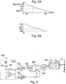
- the Figure 5A represents a variation curve of the amplitude of a pulse of the DS signal generated when a photon enters the photodiode PD, as a function of the penetration depth P of the photon in the photodiode, according to formulas (1) and (2 ).
- the curve of the Figure 5A shows that in the avalanche layer AZ (delimited by the depths Pm and PM), the voltage of a pulse generated by a photon decreases as a function of the penetration depth P of the photon.
- a photon having a wavelength less than or equal to the minimum wavelength ⁇ m generates in the signal DS a voltage pulse of amplitude Rg ⁇ k ⁇ e (G + 1), and a photon having a wavelength greater than or equal to the maximum wavelength ⁇ M generates a voltage pulse of amplitude equal to Rg ⁇ k ⁇ e.
- the signal DS does not discriminate wavelengths of photons less than the minimum wavelength ⁇ m and greater than the maximum wavelength ⁇ M.
- the photodiode can be chosen or adapted so that all the photons to be detected can reach the avalanche layer and without going beyond, with an acceptable reverse bias voltage for the photodiode.
- the photodiode can be configured so that its avalanche layer can include a range of penetration depths in the photodiode of photons to be detected, this range of depths corresponding to the wavelength range of these photons .
- the thickness of the undoped or slightly doped INT layer (which may be omitted) of the collection layer CZ may be such that the upper limit of the avalanche layer can be reached by photons having the highest small wavelength to detect.
- the lower limit of the avalanche layer may be located at a depth greater than the depth reached by photons having the longest wavelength to be detected.
- the positioning of the lower limit of the avalanche layer is related to the choice of the semiconductor material constituting the photodiode and at the depth of the pn junction in the photodiode.
- the choice of the semiconductor material constituting the photodiode also determines the penetration depths of the photons as a function of their wavelength in the material. This choice therefore influences the wavelength selectivity of the photodiode which can be defined by the ratio between a difference in depths reached by photons (substantially proportional to a difference in measured voltages), and a wavelength difference. of these photons.
- the photodiode can receive the photons not on the N + doped layer side, but on the substrate side, ie that the photons enter the diode through the substrate before reaching the P-doped layer
- the amplitude of the signal is reversed, the voltage of a pulse generated by a photon increasing with the penetration depth P of the photon, and therefore with the wavelength of the latter.
- the Figure 5B represents a curve of variation of the penetration depth of a photon in the semiconductor material constituting the photodiode PD, as a function of the wavelength of the photon. It should be noted that this curve depends essentially on the nature of the semiconductor material.
- the curve of the Figure 5B is placed in coincidence with the curve of the Figure 5A , so that the combination of these two curves shows that a photon wavelength in the range [ ⁇ m, ⁇ M] corresponds to a single pulse voltage appearing in the DS signal at the output of the PDA circuit, and vice versa.
- the PDA circuit may be associated with a circuit for determining the membership of the wavelength of an incident photon at one or more ranges of wavelengths.
- the figure 6 represents a signal generation circuit PDT representative of the illumination of the photodiode in a wavelength range, according to one embodiment.
- the signal DS is supplied to a direct input of two comparators CP1, CP2 each receiving on an inverting input a respective threshold voltage V1, V2.
- the output of the comparator CP1 is connected via an inverter I1 to a clock signal input of a counter CN1.
- the output of the comparator CP2 is connected to a clock signal input of a D-type flip-flop FF1 having a direct output Q connected to a direct input of a logic gate OG1 of type NO OR.
- the input D of the flip-flop FF1 receives the supply voltage Vcc of the circuit PDT.
- the output of the inverter I1 is also connected to an initialization control input of the flip-flop FF1.
- the gate output OG1 is connected to a counting input of the counter CN1.
- An integration control signal INT is supplied to an inverted input of the gate OG1.
- An initialization control signal RST is supplied to an initialization input of the counter CN1.
- the output of the counter CN1 provides a digital count value, for example on 8 or 16 bits, representative of the number of pulses detected by the comparator CP1, but not by the comparator CP2.
- the threshold voltages V1, V2 are chosen so as to correspond to threshold wavelengths ⁇ S1 and ⁇ S2 between the minimum wavelengths ⁇ m and maximum ⁇ M.
- the voltages V1 and V2 thus delimit a range of wavelengths [ ⁇ S2, ⁇ S1] of photons to which the photodiode PD is sensitive.
- the PDT circuit provides a numerical value representative of the number of photons having a wavelength located in the wavelength range [ ⁇ S2, ⁇ S1] having penetrated into the photodiode PD.
- the threshold voltage V1 may be chosen equal to Rg ⁇ k ⁇ e so as to correspond to the maximum wavelength ⁇ M of the photons to be detected.
- the voltage V1 can also be adjusted so as to overcome the noise.
- the Figures 7A to 7H illustrate the operation of the PDT circuit.
- the Figure 7A is a timing diagram of the DS signal.
- the FIGS. 7B, 7C, 7D and 7E are timing diagrams of the output signals of the comparators CP1, CP2 of the inverter I1 and the flip-flop FF1.
- the Figures 7F and 7G are timing diagrams of the signal INT and the output signal of the gate OG1.
- the figure 7H indicates the evolution of the value of the counter CN1 as a function of time in correspondence with the chronograms of the Figures 7A to 7G .
- the timing of the DS signal ( Figure 7A ) comprises a first pulse PS1 whose amplitude is lower than the threshold voltage V1.
- This pulse does not cause a change of state of the outputs of the comparators CP1 and CP2 which remain at 0.
- the output of the flip-flop FF1 thus remains at 0, and the output of the inverter I1 remains at 1.
- the output of the gate OG1 is at 1.
- the counter CN1 is not incremented and remains at 0 in the absence of a pulse of count provided by the inverter I1. It should be noted that as long as the signal INT is at 0, the output of the gate OG1 remains at 0. The counter CN1 can not therefore be incremented.
- the timing diagram of the signal DS then comprises a second pulse PS2 whose amplitude is greater than the threshold voltage V1, but lower than the voltage V2.
- the output of the comparator CP1 provides a pulse and the output of the comparator CP2 remains at 0.
- the output of the inverter I1 thus also provides an inverse pulse whose falling edge triggers a counting operation by the counter CN1.
- the flip-flop FF1 does not change state and the output of the gate OG1 remains at 1.
- the counter CN1 is therefore incremented by one during the counting operation.
- the rising edge of the output signal of the inverter I1 then initializes the state of the flip-flop FF1 which remains at 0.
- the timing diagram of the signal DS then comprises a third pulse PS3 whose amplitude is greater than the threshold voltages V1 and V2.
- the output of each comparator CP1, CP2 thus provides a pulse, and the output of the inverter I1 also provides an inverse pulse whose falling edge triggers a counting operation by the counter CN1.
- the output pulse of the comparator CP2 causes a change of state of the flip-flop FF1.
- the output of the gate OG1 thus goes to 0 and does not trigger an incrementation of the counter CN1 which remains at 1 during the counting operation.
- the rising edge of the output signal of the inverter I1 then triggers the initialization of the flip-flop FF1 which returns to 0, and the output signal of the gate OG1 returns to 1.
- the counter CN1 is incremented by one at the appearance of a pulse in the signal DS only when the amplitude of this pulse is between the voltages V1 and V2, and during the acquisition period of the signal of the photodiode (signal INT to 1).
- the counter CN1 therefore provides a value representative of the number of photons having reached the PD photodiode during the acquisition period and having a wavelength comprised in a delimited wavelength range. by threshold wavelengths ⁇ S1 and ⁇ S2 corresponding to the threshold voltages V1 and V2.
- the counter CN1 once read, can be initialized to 0 using the signal RST, to allow a new acquisition of the signal of the photodiode.
- each bit of the output Q of the counter CN1 can be connected to a line of an output parallel bus N1 of the image sensor by the intermediate of a selection transistor ST, for example n-channel CMOS type. All the transistors ST connected to an output bit Q of the counter CN1 are controlled by the same selection signal SEL of the pixel. When the transistors ST are turned on during a pulse provided by the signal SEL, the value of the counter CN1 is transferred to the bus N1. ⁇
- the circuit PDT can make it possible to count the photons received by the photodiode PD and having a wavelength less than the length wave ⁇ S2.
- the voltages V1 and V2 can also be modified over time to adjust the range of wavelengths of the photons to be detected.
- the PDT circuit can be used to successively and alternately detect photons in several wavelength ranges.
- the figure 8 represents a PDT1 generation circuit of signals representative of the illumination of the PD photodiode in each of two wavelength ranges, according to one embodiment.
- the circuit PDT1 differs from the PDT circuit in that it comprises two logic gates OG1, OG2 of type NO OR, and two counters CN1, CN2.
- the Q output of flip-flop FF1 is connected to an inverted input of gate OG1 and to a direct input of gate OG2.
- the signal INT is supplied to an inverted input of the gates OG1 and OG2.
- the output of the gate OG1 is connected to a counting input of the counter CN1 and the output of the gate OG2 is connected to a counting input of the counter CN2.
- the initialization signal RST is connected to an initialization control input of the counters CN1, CN2.
- the DS signal pulses provided by the PDA circuit following the reception of a photon by the PD photodiode are compared with the threshold voltages V1 and V2.
- the impulses higher than the threshold voltage V1 and lower than the threshold voltage V2 increment the counter CN1 and the pulses higher than the threshold voltage V2 increment the counter CN2.
- the bits of the output Q of each counter CN1, CN2 can be connected to a respective line of an output parallel bus N1, N2 of the image sensor, via ST selection transistors whose gate is controlled by a single pixel selection signal SEL.
- the values of the counters CN1, CN2 can be transferred on the buses N1, N2.
- the counters can be reset by a pulse provided by the initialization signal RST.
- the figure 9 represents a PDT2 generation circuit of signals representative of the illumination of the photodiode in four wavelength ranges, according to one embodiment.
- the circuit PDT2 differs from the circuit PDT in that it comprises two additional comparators CP3, CP4 for comparing the signal DS with two additional threshold voltages V3, V4, such that V1 ⁇ V2 ⁇ V3 ⁇ V4.
- the voltage V3 delimits with the voltage V2 a second range of wavelengths and with the voltage V4 a third range of wavelengths.
- the voltage V4 delimits a fourth wavelength range located beyond the wavelength corresponding to this voltage.
- the PDT2 circuit also comprises two additional D type FF2, FF3 type flip-flops, three additional OG2, OG3, OG4 logic gates, and three additional CN2, CN3, CN4 counters.
- the output of the inverter I1 is connected to a clock signal input of the counters CN1 to CN4.
- the integration signal INT is supplied to an inverted input of each of the gates OG1 to OG4.
- the input D of the flip-flops FF1 to FF3 receives the supply voltage Vcc of the circuit PDT2.
- the Q output of flip-flop FF1 is connected to a direct input of gate OG1 and to an inverted input of gate OG2.
- the output of comparator CP3 is connected to a clock signal input of flip-flop FF2.
- the Q output of the flip-flop FF2 is connected to a direct input of the OG1 and OG2 gates and to an inverted input of the OG3 gate.
- the output of the comparator CP4 is connected to a clock signal input of the flip flop FF3.
- the output Q of the flip-flop FF3 is connected to a direct input of the gates OG1, OG2 and OG3 and to an inverted input of the gate OG4.
- the output of each gate OG1 to OG4 is connected to a counting input of one of the counters CN1 to CN4.
- the counter CN1 is incremented by one during an acquisition period (signal INT at 1) when the photodiode PD receives a photon whose wavelength is between two wavelengths respectively corresponding to the voltages V1 and V2.
- the counter CN2 is incremented by one during the acquisition period when the photodiode PD receives a photon whose wavelength is between two wavelengths respectively corresponding to the voltages V2 and V3.
- the counter CN3 is incremented by one during the acquisition period when the photodiode PD receives a photon whose wavelength is between two wavelengths respectively corresponding to the voltages V3 and V4.
- the counter CN4 is incremented by one during the acquisition period when the photodiode PD receives a photon whose wavelength is less than the wavelength corresponding to the voltage V4. It should be noted that if it is not desired to detect photons whose wavelength is less than the wavelength corresponding to the voltage V4, the gate OG4 and the counter CN4 may be omitted.
- each bit of the output Q of each counter CN1 to CN4 can be connected to a line of an output bus N1, N2, N3, N4 of the image sensor via a selection transistor ST. All the transistors ST connected to an output bit Q of one of the counters CN1 to CN4 are controlled by the same pixel selection signal SEL.
- the values of the counters CN1 to CN4 can be transferred on the buses N1 to N4.
- the counters can be reset by a pulse provided by the initialization signal RST.
- the PDT2 circuit thus makes it possible with a single photodiode to provide several signals representative of the reception by a single photodiode of photons respectively in several ranges of wavelengths.
- wavelength ranges can thus be discriminated by providing other comparators to compare the DS signal with other threshold voltages corresponding to other wavelength range limits. It may also be provided that the wavelength ranges discriminated by the comparators partially overlap, by adjusting the threshold voltages V1 to V4 so as to form partially overlapping voltage ranges. It can also be envisaged to reject one or more wavelength ranges, for example by removing one of the gates OG1 to OG4 and the counter CN1 to CN4 connected to the gated gate, so as not to perform counting. output pulse of the amplifier TA when the amplitude of this pulse is between two of the voltages V1 to V4.
- the present invention is capable of various alternative embodiments and various applications.
- the invention is not limited to the use of a photodiode having no collection layer. It is simply important that the avalanche layer of the photodiode be compatible with the range of photon wavelengths to be detected. Since this condition can be realized, the present invention can be applied to all wavelength bands.
- the circuits of the figures 6 , 8 and 9 perform a conversion of current pulses from the photodiode into voltage pulses and a comparison of the voltage pulses with voltage thresholds. These circuits can of course be easily modified to amplify the current pulses and compare these amplified current pulses with current thresholds.
- the detection device just described can be advantageously used in many applications.
- the detection device can provide images simultaneously in different spectral bands.
- current devices can only perform such observations in different spectral bands sequentially.
- the detection device can also be applied to hyperspectral vision. Indeed, the detection device proves particularly suitable for simultaneous vision in several bands narrow and contiguous.
- the detection device can also perform the function of pre-disperser in a cross-dispersion spectroscope to sort the orders of a network or an interferometer.
- the device can discriminate excitation photons, fluorescent photons, and bioluminescent markers, as long as they have different wavelengths.
- the detection device can also be used in the infrared range to determine the absolute temperature of an observed body, by detecting photons simultaneously two or more spectral bands.
- the detection device is also particularly suitable for DWDM (Dense Wavelength Division Multiplexing) communications consisting of transmitting an optical fiber several laser communications at different wavelengths.
- the sensing device can also be used in particle physics to determine the energy (i.e. wavelength) of photons.
- the simplicity and therefore the speed of the logic circuits for processing the detected signals makes the detection device particularly suitable for the determination with a great accuracy of the flight time of a photon in a LADAR system (laser radar) when the detection is synchronized with a pulsed laser, or in a positron emission tomography system.
- LADAR system laser radar
Landscapes
- Physics & Mathematics (AREA)
- Spectroscopy & Molecular Physics (AREA)
- General Physics & Mathematics (AREA)
- Light Receiving Elements (AREA)
- Photometry And Measurement Of Optical Pulse Characteristics (AREA)
- Engineering & Computer Science (AREA)
- Multimedia (AREA)
- Signal Processing (AREA)
Claims (13)
- Verfahren zur Photonendetektion, das einen Ablaufschritt umfasst, eine Fotodiode, die in einem Halbleitermaterial ausgebildet ist, einer Polarisierungsspannung (BV) zu unterwerfen, so dass ein Lawinenphänomen in einer Lawinenschicht (AZ) der Fotodiode ausgelöst wird, wenn ein Photon (PH, PH1) in die Fotodiode eindringt,
dadurch gekennzeichnet, dass die Lawinenschicht (AZ) sich in dem Halbleitermaterial von einer minimalen Tiefe (Pm) zu einer maximalen Tiefe (PM) erstreckt, so dass sie von den Photonen (PH, PH1) erreicht werden kann, die eine Wellenlänge aufweisen, die zwischen der minimalen und der maximalen Wellenlänge (Am, AM) liegt, wobei das Verfahren die Ablaufschritte umfasst: Vergleich der Amplitude des Signals (DS), das von der Fotodiode bereitgestellt wird, bei zwei verschiedenen Schwellenwerten (V1, V2), und die Herleitung, dass die Fotodiode ein Photon empfangen hat, das eine Wellenlänge aufweist, die zwischen zwei Grenzwellenlängen (AS1, λS2) liegt, die zwischen der minimalen und der maximalen Wellenlänge liegen, falls die Signalamplitude zwischen den zwei Schwellenwerten liegt. - Verfahren nach Anspruch 1, das die Ablaufschritte der Zählung einer Anzahl von Impulsen während einer Erfassungsperiode umfasst, die an den Polklemmen der Fotodiode (PD) erfasst wurden, die eine Amplitude aufweisen, die zwischen den zwei Schwellenwerten (V1, V2) liegt, um einen repräsentativen Wert einer Anzahl von Photonen (PH, PH1) zu erlangen, die während der Erfassungsperiode in die Fotodiode (PD) eingedrungen sind, und die eine Wellenlänge aufweisen, die zwischen den beiden Grenzwellenlängen (λS1, λS2) liegt.
- Verfahren nach Anspruch 1 oder 2, das die Ablaufschritte der Zählung einer Anzahl von Impulsen während einer Erfassungsperiode umfasst, die an den Polklemmen der Fotodiode (PD) erfasst wurden, die eine höhere Amplitude als der größere der zwei Schwellenwerte (V2) aufweisen, um einen repräsentativen Wert einer Anzahl von Photonen (PH, PH1) zu erlange, die während der Erfassungsperiode in die Fotodiode (PD) eingedrungen sind, und die die eine untere Wellenlänge aufweisen, die niedriger als die kleinere der zwei Grenzwellenlängen (λS2) ist.
- Verfahren nach einem der Ansprüche 1 bis 3, in dem der kleinere der zwei Schwellenwerte (V1) einer äußersten Wellenlänge (λS1) des zu erfassenden Photons entspricht.
- Verfahren nach einem der Ansprüche 1 bis 4, das die Ablaufschritte umfasst: Vergleich der Amplitude eines Signals (DS), das von der Fotodiode bei mehreren anderen Schwellenwerten (V3, V4) bereitgestellt wird, um mit den zwei Schwellenwerten (V1, V2) mehrere Wertebereiche der Amplitude einzugrenzen, und Zählung der Anzahl von Impulsen des Signals (DS) in jedem der Wertebereiche der Amplitude während einer Erfassungsperiode.
- Verfahren nach Anspruch 5, in dem die Wertbereiche der Amplitude, die von den Schwellenwerten (V1, V2, V3, V4) eingegrenzt werden, nicht aneinander angrenzend sind und/oder sich nicht überlappen.
- Verfahren nach einem der Ansprüche 1 bis 6, das einen Ablaufschritt der Anpassung der Schwellenwerte umfasst, um die Bereiche der Wellenlänge anzupassen, in denen die Photonen zu erfassen sind.
- Verfahren nach einem der Ansprüche 1 bis 7, das einen Ablaufschritt der Anpassung der Polarisierungsspannung der Fotodiode umfasst, damit alle zu erfassenden Photonen die Lawinenschicht erreichen können und ohne darüber hinaus zu gehen.
- Vorrichtung zur Photonendetektion, die eine Fotodiode umfasst, die in einem Halbleitermaterial ausgebildet ist und einer Polarisierungsspannung (BV) unterworfen ist, so dass ein Lawinenphänomen in einer Lawinenschicht (AZ) der Fotodiode ausgelöst wird, wenn ein Photon (PH, PH1) in die Fotodiode eindringt,
dadurch gekennzeichnet, dass die Lawinenschicht (AZ) sich in dem Halbleitermaterial von einer minimalen Tiefe (Pm) zu einer maximalen Tiefe (PM) erstreckt, so dass sie von den Photonen (PH, PH1) erreicht werden kann, die eine Wellenlänge aufweisen, die zwischen der minimalen und der maximalen Wellenlänge (Am, AM) liegt, wobei die Vorrichtung ausgestaltet ist für:Vergleichen der Amplitude eines Signals (DS), das von der Fotodiode bereitgestellt wird, bei zwei verschiedenen Schwellenwerten (V1, V2), undBestimmen, dass die Fotodiode ein Photon empfangen hat, das eine Wellenlänge aufweist, die zwischen zwei Grenzwellenlängen (λS1, λS2) liegt, die zwischen der minimalen und der maximalen Wellenlänge liegen, falls die Signalamplitude zwischen den zwei Schwellenwerten liegt. - Vorrichtung nach Anspruch 9, die dazu ausgestaltet ist, das Verfahren nach einem der Ansprüche 2 bis 8 umzusetzen.
- Vorrichtung nach Anspruch 9 oder 10, in der die Fotodiode (PD) eine Sammelschicht (CZ) von niedriger Dotierung oder nicht dotiert umfasst, deren Dicke reduziert ist, so dass die Lawinenschicht (AZ) sich mindestens bis in eine Tiefe erstrecken kann, die von den Photonen mit einer äußersten zu erfassenden Wellenlänge erreicht wird.
- Vorrichtung nach einem der Ansprüche 9 bis 11, in der die Fotodiode (PD) eine Sperrschicht pn umfasst, die in einer bestimmten Tiefe in dem Halbleitermaterial realisiert ist, wobei das Halbleitermaterial und die Tiefe der Sperrschicht so gewählt sind, dass das Halbleitermaterial von den zu erfassenden Photonen bis zu einer Tiefe durchquert werden kann, die geeignet ist, in der Lawinenschicht (AZ) der Fotodiode zu liegen.
- Bildgebungsvorrichtung, die mehrere Detektionsvorrichtungen nach einem der Ansprüche 9 bis 12 umfasst, wobei die Fotodioden (PD) der Detektionsvorrichtungen in einer Matrixkonfiguration angeordnet sind.
Applications Claiming Priority (2)
| Application Number | Priority Date | Filing Date | Title |
|---|---|---|---|
| FR1004866A FR2968836B1 (fr) | 2010-12-14 | 2010-12-14 | Photodetecteur ayant une sensibilite spectrale |
| PCT/EP2011/072618 WO2012080256A2 (fr) | 2010-12-14 | 2011-12-13 | Photodetecteur ayant une sensibilite spectrale |
Publications (2)
| Publication Number | Publication Date |
|---|---|
| EP2652792A2 EP2652792A2 (de) | 2013-10-23 |
| EP2652792B1 true EP2652792B1 (de) | 2018-09-12 |
Family
ID=45558669
Family Applications (1)
| Application Number | Title | Priority Date | Filing Date |
|---|---|---|---|
| EP11815441.8A Not-in-force EP2652792B1 (de) | 2010-12-14 | 2011-12-13 | Fotodetektor mit spektraler empfindlichkeit |
Country Status (5)
| Country | Link |
|---|---|
| US (1) | US9482578B2 (de) |
| EP (1) | EP2652792B1 (de) |
| FR (1) | FR2968836B1 (de) |
| IL (1) | IL226922A (de) |
| WO (1) | WO2012080256A2 (de) |
Families Citing this family (2)
| Publication number | Priority date | Publication date | Assignee | Title |
|---|---|---|---|---|
| EP3472866A4 (de) * | 2016-06-21 | 2020-02-12 | Shenzhen Genorivision Technology Co., Ltd. | Bildsensor mit grossem dynamikbereich |
| JP7339780B2 (ja) * | 2019-06-07 | 2023-09-06 | キヤノン株式会社 | 撮像装置及びその制御方法 |
Citations (1)
| Publication number | Priority date | Publication date | Assignee | Title |
|---|---|---|---|---|
| US20060131480A1 (en) * | 2004-01-12 | 2006-06-22 | Edoardo Charbon | Method for controlling the spectral response of light sensitive elements, and image sensor with a controllable spectral response |
Family Cites Families (9)
| Publication number | Priority date | Publication date | Assignee | Title |
|---|---|---|---|---|
| JPH07240534A (ja) * | 1993-03-16 | 1995-09-12 | Seiko Instr Inc | 光電変換半導体装置及びその製造方法 |
| US5782756A (en) * | 1996-09-19 | 1998-07-21 | Nellcor Puritan Bennett Incorporated | Method and apparatus for in vivo blood constituent analysis |
| US5965875A (en) * | 1998-04-24 | 1999-10-12 | Foveon, Inc. | Color separation in an active pixel cell imaging array using a triple-well structure |
| EP1164401B1 (de) * | 2000-06-17 | 2005-03-09 | Leica Microsystems Heidelberg GmbH | Verschränkte-Photonen-Mikroskop |
| US7160753B2 (en) * | 2004-03-16 | 2007-01-09 | Voxtel, Inc. | Silicon-on-insulator active pixel sensors |
| US20060231913A1 (en) * | 2005-04-13 | 2006-10-19 | Clifton Labs, Inc. | Method for determining wavelengths of light incident on a stacked photodetector structure |
| JP4277826B2 (ja) * | 2005-06-23 | 2009-06-10 | 住友電気工業株式会社 | 窒化物結晶、窒化物結晶基板、エピ層付窒化物結晶基板、ならびに半導体デバイスおよびその製造方法 |
| JP4654446B2 (ja) * | 2007-03-28 | 2011-03-23 | 独立行政法人国立高等専門学校機構 | アバランシェフォトダイオードを用いた波長スペクトル検出方法 |
| US20100316184A1 (en) * | 2008-10-17 | 2010-12-16 | Jan Iwanczyk | Silicon photomultiplier detector for computed tomography |
-
2010
- 2010-12-14 FR FR1004866A patent/FR2968836B1/fr not_active Expired - Fee Related
-
2011
- 2011-12-13 US US13/994,392 patent/US9482578B2/en not_active Expired - Fee Related
- 2011-12-13 WO PCT/EP2011/072618 patent/WO2012080256A2/fr not_active Ceased
- 2011-12-13 EP EP11815441.8A patent/EP2652792B1/de not_active Not-in-force
-
2013
- 2013-06-13 IL IL226922A patent/IL226922A/en active IP Right Grant
Patent Citations (1)
| Publication number | Priority date | Publication date | Assignee | Title |
|---|---|---|---|---|
| US20060131480A1 (en) * | 2004-01-12 | 2006-06-22 | Edoardo Charbon | Method for controlling the spectral response of light sensitive elements, and image sensor with a controllable spectral response |
Also Published As
| Publication number | Publication date |
|---|---|
| US20130335742A1 (en) | 2013-12-19 |
| IL226922A (en) | 2017-02-28 |
| FR2968836A1 (fr) | 2012-06-15 |
| US9482578B2 (en) | 2016-11-01 |
| WO2012080256A2 (fr) | 2012-06-21 |
| FR2968836B1 (fr) | 2013-03-22 |
| EP2652792A2 (de) | 2013-10-23 |
| WO2012080256A3 (fr) | 2013-05-23 |
Similar Documents
| Publication | Publication Date | Title |
|---|---|---|
| EP3503192B1 (de) | Bilderfassungsvorrichtung für ein 2d-bild und ein tiefenbild einer szene | |
| EP3104421B1 (de) | Mit einem gitter abgedeckte spad-fotodiode | |
| Buttafava et al. | SPAD-based asynchronous-readout array detectors for image-scanning microscopy | |
| US7608823B2 (en) | Multimode focal plane array with electrically isolated commons for independent sub-array biasing | |
| EP2636066B1 (de) | Detektor für sichtbare und nahinfrarot-strahlung | |
| EP2636067B1 (de) | Detektor für sichtbare und nahinfrarot-strahlung | |
| EP2184788B1 (de) | Photodetektor mit interner Verstärkung und Detektor, der eine Matrix von solchen Photodetektoren enthält | |
| BE1022761B1 (fr) | Couche de blocage perforee pour une amelioration de la reponse a large bande dans un reseau de plan focal. | |
| FR2983348A1 (fr) | Bloc detecteur optique | |
| FR3071788A1 (fr) | Systeme d'observation de conducteur et son procede de saisie par le systeme et le procede de fabrication du systeme | |
| EP2752893A1 (de) | Halbleiterstruktur vom Typ Avalanche-Fotodiode, und Herstellungsverfahren einer solchen Struktur | |
| EP1903612B1 (de) | Fotodiode mit Lawine | |
| Incoronato et al. | Multi-channel SPAD chip for silicon photonics with multi-photon coincidence detection | |
| EP3155662B1 (de) | Struktur einer ausleseschaltung mit ladungsinjektion | |
| EP1231642A1 (de) | Photodetektor mit drei Transistoren | |
| EP2652792B1 (de) | Fotodetektor mit spektraler empfindlichkeit | |
| WO2014091093A1 (fr) | Imageur monolithique multispectral visible et infrarouge | |
| EP2801115B1 (de) | Fotodetektor | |
| EP3471151B1 (de) | Helmholtz-resonator-photodetektor | |
| WO2015004235A1 (fr) | Photodetecteur semi-transparent a jonction p-n structuree | |
| WO2004057678A1 (fr) | Dispositif de detection de lumiere a filtre integre | |
| EP3413035B1 (de) | Verfahren zur bestimmung von abfallzeiten eines lumineszenzsignals | |
| EP2382672B1 (de) | Verfahren zur herstellung einer photodiode und entsprechende photodiode und detektor für electromagnetische strahlung | |
| FR3156991A1 (fr) | Dispositif électronique de capture et d’affichage d’images | |
| FR2945668A1 (fr) | Capteur d'image pour imagerie a tres bas niveau de lumiere. |
Legal Events
| Date | Code | Title | Description |
|---|---|---|---|
| PUAI | Public reference made under article 153(3) epc to a published international application that has entered the european phase |
Free format text: ORIGINAL CODE: 0009012 |
|
| 17P | Request for examination filed |
Effective date: 20130610 |
|
| AK | Designated contracting states |
Kind code of ref document: A2 Designated state(s): AL AT BE BG CH CY CZ DE DK EE ES FI FR GB GR HR HU IE IS IT LI LT LU LV MC MK MT NL NO PL PT RO RS SE SI SK SM TR |
|
| RIN1 | Information on inventor provided before grant (corrected) |
Inventor name: GACH, JEAN-LUC |
|
| DAX | Request for extension of the european patent (deleted) | ||
| 17Q | First examination report despatched |
Effective date: 20170522 |
|
| GRAP | Despatch of communication of intention to grant a patent |
Free format text: ORIGINAL CODE: EPIDOSNIGR1 |
|
| INTG | Intention to grant announced |
Effective date: 20180403 |
|
| RAP1 | Party data changed (applicant data changed or rights of an application transferred) |
Owner name: UNIVERSITE D'AIX-MARSEILLE |
|
| GRAS | Grant fee paid |
Free format text: ORIGINAL CODE: EPIDOSNIGR3 |
|
| GRAA | (expected) grant |
Free format text: ORIGINAL CODE: 0009210 |
|
| AK | Designated contracting states |
Kind code of ref document: B1 Designated state(s): AL AT BE BG CH CY CZ DE DK EE ES FI FR GB GR HR HU IE IS IT LI LT LU LV MC MK MT NL NO PL PT RO RS SE SI SK SM TR |
|
| REG | Reference to a national code |
Ref country code: GB Ref legal event code: FG4D Free format text: NOT ENGLISH |
|
| REG | Reference to a national code |
Ref country code: CH Ref legal event code: EP |
|
| REG | Reference to a national code |
Ref country code: IE Ref legal event code: FG4D Free format text: LANGUAGE OF EP DOCUMENT: FRENCH |
|
| REG | Reference to a national code |
Ref country code: AT Ref legal event code: REF Ref document number: 1041595 Country of ref document: AT Kind code of ref document: T Effective date: 20181015 |
|
| REG | Reference to a national code |
Ref country code: DE Ref legal event code: R096 Ref document number: 602011052036 Country of ref document: DE |
|
| REG | Reference to a national code |
Ref country code: NL Ref legal event code: MP Effective date: 20180912 |
|
| REG | Reference to a national code |
Ref country code: LT Ref legal event code: MG4D |
|
| PG25 | Lapsed in a contracting state [announced via postgrant information from national office to epo] |
Ref country code: GR Free format text: LAPSE BECAUSE OF FAILURE TO SUBMIT A TRANSLATION OF THE DESCRIPTION OR TO PAY THE FEE WITHIN THE PRESCRIBED TIME-LIMIT Effective date: 20181213 Ref country code: NO Free format text: LAPSE BECAUSE OF FAILURE TO SUBMIT A TRANSLATION OF THE DESCRIPTION OR TO PAY THE FEE WITHIN THE PRESCRIBED TIME-LIMIT Effective date: 20181212 Ref country code: LT Free format text: LAPSE BECAUSE OF FAILURE TO SUBMIT A TRANSLATION OF THE DESCRIPTION OR TO PAY THE FEE WITHIN THE PRESCRIBED TIME-LIMIT Effective date: 20180912 Ref country code: BG Free format text: LAPSE BECAUSE OF FAILURE TO SUBMIT A TRANSLATION OF THE DESCRIPTION OR TO PAY THE FEE WITHIN THE PRESCRIBED TIME-LIMIT Effective date: 20181212 Ref country code: SE Free format text: LAPSE BECAUSE OF FAILURE TO SUBMIT A TRANSLATION OF THE DESCRIPTION OR TO PAY THE FEE WITHIN THE PRESCRIBED TIME-LIMIT Effective date: 20180912 Ref country code: RS Free format text: LAPSE BECAUSE OF FAILURE TO SUBMIT A TRANSLATION OF THE DESCRIPTION OR TO PAY THE FEE WITHIN THE PRESCRIBED TIME-LIMIT Effective date: 20180912 Ref country code: FI Free format text: LAPSE BECAUSE OF FAILURE TO SUBMIT A TRANSLATION OF THE DESCRIPTION OR TO PAY THE FEE WITHIN THE PRESCRIBED TIME-LIMIT Effective date: 20180912 |
|
| PG25 | Lapsed in a contracting state [announced via postgrant information from national office to epo] |
Ref country code: AL Free format text: LAPSE BECAUSE OF FAILURE TO SUBMIT A TRANSLATION OF THE DESCRIPTION OR TO PAY THE FEE WITHIN THE PRESCRIBED TIME-LIMIT Effective date: 20180912 Ref country code: LV Free format text: LAPSE BECAUSE OF FAILURE TO SUBMIT A TRANSLATION OF THE DESCRIPTION OR TO PAY THE FEE WITHIN THE PRESCRIBED TIME-LIMIT Effective date: 20180912 Ref country code: HR Free format text: LAPSE BECAUSE OF FAILURE TO SUBMIT A TRANSLATION OF THE DESCRIPTION OR TO PAY THE FEE WITHIN THE PRESCRIBED TIME-LIMIT Effective date: 20180912 |
|
| REG | Reference to a national code |
Ref country code: AT Ref legal event code: MK05 Ref document number: 1041595 Country of ref document: AT Kind code of ref document: T Effective date: 20180912 |
|
| PG25 | Lapsed in a contracting state [announced via postgrant information from national office to epo] |
Ref country code: EE Free format text: LAPSE BECAUSE OF FAILURE TO SUBMIT A TRANSLATION OF THE DESCRIPTION OR TO PAY THE FEE WITHIN THE PRESCRIBED TIME-LIMIT Effective date: 20180912 Ref country code: PL Free format text: LAPSE BECAUSE OF FAILURE TO SUBMIT A TRANSLATION OF THE DESCRIPTION OR TO PAY THE FEE WITHIN THE PRESCRIBED TIME-LIMIT Effective date: 20180912 Ref country code: AT Free format text: LAPSE BECAUSE OF FAILURE TO SUBMIT A TRANSLATION OF THE DESCRIPTION OR TO PAY THE FEE WITHIN THE PRESCRIBED TIME-LIMIT Effective date: 20180912 Ref country code: IT Free format text: LAPSE BECAUSE OF FAILURE TO SUBMIT A TRANSLATION OF THE DESCRIPTION OR TO PAY THE FEE WITHIN THE PRESCRIBED TIME-LIMIT Effective date: 20180912 Ref country code: IS Free format text: LAPSE BECAUSE OF FAILURE TO SUBMIT A TRANSLATION OF THE DESCRIPTION OR TO PAY THE FEE WITHIN THE PRESCRIBED TIME-LIMIT Effective date: 20190112 Ref country code: RO Free format text: LAPSE BECAUSE OF FAILURE TO SUBMIT A TRANSLATION OF THE DESCRIPTION OR TO PAY THE FEE WITHIN THE PRESCRIBED TIME-LIMIT Effective date: 20180912 Ref country code: NL Free format text: LAPSE BECAUSE OF FAILURE TO SUBMIT A TRANSLATION OF THE DESCRIPTION OR TO PAY THE FEE WITHIN THE PRESCRIBED TIME-LIMIT Effective date: 20180912 Ref country code: CZ Free format text: LAPSE BECAUSE OF FAILURE TO SUBMIT A TRANSLATION OF THE DESCRIPTION OR TO PAY THE FEE WITHIN THE PRESCRIBED TIME-LIMIT Effective date: 20180912 Ref country code: ES Free format text: LAPSE BECAUSE OF FAILURE TO SUBMIT A TRANSLATION OF THE DESCRIPTION OR TO PAY THE FEE WITHIN THE PRESCRIBED TIME-LIMIT Effective date: 20180912 |
|
| PG25 | Lapsed in a contracting state [announced via postgrant information from national office to epo] |
Ref country code: SK Free format text: LAPSE BECAUSE OF FAILURE TO SUBMIT A TRANSLATION OF THE DESCRIPTION OR TO PAY THE FEE WITHIN THE PRESCRIBED TIME-LIMIT Effective date: 20180912 Ref country code: PT Free format text: LAPSE BECAUSE OF FAILURE TO SUBMIT A TRANSLATION OF THE DESCRIPTION OR TO PAY THE FEE WITHIN THE PRESCRIBED TIME-LIMIT Effective date: 20190112 Ref country code: SM Free format text: LAPSE BECAUSE OF FAILURE TO SUBMIT A TRANSLATION OF THE DESCRIPTION OR TO PAY THE FEE WITHIN THE PRESCRIBED TIME-LIMIT Effective date: 20180912 |
|
| REG | Reference to a national code |
Ref country code: DE Ref legal event code: R097 Ref document number: 602011052036 Country of ref document: DE |
|
| REG | Reference to a national code |
Ref country code: DE Ref legal event code: R119 Ref document number: 602011052036 Country of ref document: DE |
|
| PLBE | No opposition filed within time limit |
Free format text: ORIGINAL CODE: 0009261 |
|
| STAA | Information on the status of an ep patent application or granted ep patent |
Free format text: STATUS: NO OPPOSITION FILED WITHIN TIME LIMIT |
|
| PG25 | Lapsed in a contracting state [announced via postgrant information from national office to epo] |
Ref country code: DK Free format text: LAPSE BECAUSE OF FAILURE TO SUBMIT A TRANSLATION OF THE DESCRIPTION OR TO PAY THE FEE WITHIN THE PRESCRIBED TIME-LIMIT Effective date: 20180912 |
|
| REG | Reference to a national code |
Ref country code: CH Ref legal event code: PL |
|
| 26N | No opposition filed |
Effective date: 20190613 |
|
| GBPC | Gb: european patent ceased through non-payment of renewal fee |
Effective date: 20181213 |
|
| PG25 | Lapsed in a contracting state [announced via postgrant information from national office to epo] |
Ref country code: LU Free format text: LAPSE BECAUSE OF NON-PAYMENT OF DUE FEES Effective date: 20181213 Ref country code: MC Free format text: LAPSE BECAUSE OF FAILURE TO SUBMIT A TRANSLATION OF THE DESCRIPTION OR TO PAY THE FEE WITHIN THE PRESCRIBED TIME-LIMIT Effective date: 20180912 Ref country code: SI Free format text: LAPSE BECAUSE OF FAILURE TO SUBMIT A TRANSLATION OF THE DESCRIPTION OR TO PAY THE FEE WITHIN THE PRESCRIBED TIME-LIMIT Effective date: 20180912 |
|
| REG | Reference to a national code |
Ref country code: IE Ref legal event code: MM4A |
|
| REG | Reference to a national code |
Ref country code: BE Ref legal event code: MM Effective date: 20181231 |
|
| PG25 | Lapsed in a contracting state [announced via postgrant information from national office to epo] |
Ref country code: FR Free format text: LAPSE BECAUSE OF NON-PAYMENT OF DUE FEES Effective date: 20181231 Ref country code: IE Free format text: LAPSE BECAUSE OF NON-PAYMENT OF DUE FEES Effective date: 20181213 Ref country code: DE Free format text: LAPSE BECAUSE OF NON-PAYMENT OF DUE FEES Effective date: 20190702 |
|
| PG25 | Lapsed in a contracting state [announced via postgrant information from national office to epo] |
Ref country code: BE Free format text: LAPSE BECAUSE OF NON-PAYMENT OF DUE FEES Effective date: 20181231 |
|
| PG25 | Lapsed in a contracting state [announced via postgrant information from national office to epo] |
Ref country code: LI Free format text: LAPSE BECAUSE OF NON-PAYMENT OF DUE FEES Effective date: 20181231 Ref country code: GB Free format text: LAPSE BECAUSE OF NON-PAYMENT OF DUE FEES Effective date: 20181213 Ref country code: CH Free format text: LAPSE BECAUSE OF NON-PAYMENT OF DUE FEES Effective date: 20181231 |
|
| PG25 | Lapsed in a contracting state [announced via postgrant information from national office to epo] |
Ref country code: MT Free format text: LAPSE BECAUSE OF FAILURE TO SUBMIT A TRANSLATION OF THE DESCRIPTION OR TO PAY THE FEE WITHIN THE PRESCRIBED TIME-LIMIT Effective date: 20180912 |
|
| PG25 | Lapsed in a contracting state [announced via postgrant information from national office to epo] |
Ref country code: TR Free format text: LAPSE BECAUSE OF FAILURE TO SUBMIT A TRANSLATION OF THE DESCRIPTION OR TO PAY THE FEE WITHIN THE PRESCRIBED TIME-LIMIT Effective date: 20180912 |
|
| PG25 | Lapsed in a contracting state [announced via postgrant information from national office to epo] |
Ref country code: HU Free format text: LAPSE BECAUSE OF FAILURE TO SUBMIT A TRANSLATION OF THE DESCRIPTION OR TO PAY THE FEE WITHIN THE PRESCRIBED TIME-LIMIT; INVALID AB INITIO Effective date: 20111213 Ref country code: CY Free format text: LAPSE BECAUSE OF FAILURE TO SUBMIT A TRANSLATION OF THE DESCRIPTION OR TO PAY THE FEE WITHIN THE PRESCRIBED TIME-LIMIT Effective date: 20180912 Ref country code: MK Free format text: LAPSE BECAUSE OF NON-PAYMENT OF DUE FEES Effective date: 20180912 |